 Open Access Article
Optimized hot injection and HCl purification for high quality Cu2ZnSnS4 nanoparticles†
Amin Hasan Husien *ab,
Giorgio Tseberlidis
 *a,
Vanira Trifiletti
 a,
Elisa Fabbretti
 a,
Silvia Mostoni
 a,
James McGettrick
 c,
Trystan Watson
 c,
Riccardo Po
 b and
Simona Binetti
 a
a
aDepartment of Materials Science and Solar Energy Research Center (MIB-SOLAR), University of Milano-Bicocca, Via Cozzi 55, I-20125, Milan, Italy. E-mail: giorgio.tseberlidis@unimib.it; aminhasan.husien@unimib.it
bNew Energies, Renewable Energies and Materials Science Research Center Istituto Donegani, Eni S.p.A., via Fauser 4, I-28100, Novara, Italy
cSPECIFIC IKC, Faculty of Science and Engineering, Swansea University, Fabian Way, Swansea, SA1 8EN, UK
First published on 18th November 2024
Abstract
Cu2ZnSnS4 (CZTS) is a narrow band gap, non-toxic, and environmentally friendly semiconductor with important properties for photovoltaic and electro-/photo-catalytic applications. In this study, we report on the synthesis of CZTS nanoparticles (NPs) by a simple and promising hot-injection technique using environmentally friendly, earth-abundant, and low-cost copper and zinc acetates in combination with tin chloride and elemental sulphur. Oleylamine was used as solvent and capping agent. The influence of injection temperatures on the crystalline size, morphology and crystal structure were studied. The formation of detrimental phases has been investigated, as well as their removal by using an HCl treatment during the purification step of the CZTS NPs synthesis process. Raman spectroscopy, X-ray diffraction (XRD), energy-dispersive X-ray spectroscopy (EDX), transmission electron microscopy (TEM), and scanning electron microscopy (SEM) analyses were used to investigate the formation mechanism of the CZTS NPs. The experimental results showed that the injection temperature influences the NPs growth. Thermogravimetric analysis (TGA), X-ray photoelectron spectroscopy (XPS) and infrared spectroscopy (FTIR-ATR) analyses were used to confirm the removal of both organic traces and detrimental phases. It was found that HCl treatment plays a key role in the successful removal of impurities without altering the final crystalline composition profile or NPs surface.
Introduction
The kesterite compound Cu2ZnSnS4 (CZTS), which consists of low-toxicity, cheap and earth-abundant elements, has been developed as a promising candidate to replace the expensive and/or toxic light absorber materials, namely CdTe and Cu(In,Ga)Se2, commonly used in thin-film photovoltaic devices. In addition to its earth-abundance and eco-compatibility, CZTS exhibits p-type conductivity with a large absorption coefficient (≥104 cm−1) and a suitable direct band gap ranging between 1.4 and 1.6 eV, which makes it very attractive for solar energy conversion devices.1–4 Additionally, it has been successfully employed as photocatalyst, even though the research in this field is still in its infancy.5–9 This provides a solid incentive to continue developing and optimizing CZTS-based technologies and designing production processes compatible with industrial scale-up and mass production.Hitherto, CZTS thin films have been grown by several techniques, including vacuum-based techniques like radio-frequency (RF) magnetron10 and direct current (DC) sputtering,11,12 pulsed laser deposition13 and thermal evaporation;14 non-vacuum methods such as hydrazine-based,15,16 sol–gel,12,17–22 spray pyrolysis23 and nanoparticle-based methods.24–28 Among them, procedures for producing CZTS thin films starting from CZTS nanoparticles (NPs) have emerged as a promising approach because of its cost-effectiveness, scalability, and simplicity, since they eliminate the need for expensive vacuum instruments and lead to materials of good quality.29 Notably, these methods enable precise control of the precursor composition without needing high-temperature annealing and requiring a low amount of precursors, overall contributing to the reduction of the production costs. Furthermore, this approach can provide homogeneous thin films and nanocrystals with specifically tuned energy band gap and optoelectrical properties.30 Besides, nanocrystal inks produced using NPs-based methods have several advantages; the inks are chemically adaptable, their viscosity is easily manageable, and they can be employed in a variety of application techniques, such as roll-to-roll coating, inkjet-printing, dip-coating, and spray coating onto a variety of substrates under ambient conditions.31–34 A technique commonly used for the synthesis of NPs is the hot injection method, in the field of colloidal nanocrystal synthesis,35,36 that involves the rapid injection of a precursor solution into a second hot one under controlled conditions. This method enables a good control of the NPs nucleation and growth as well as the kinetics to obtain monodisperse NPs with a high yield.37,38 Nevertheless, according to the phase diagram of CZTS, a high quality CZTS without impurities is challenging to achieve due to the very narrow phase stability range, which is usually matched with the formation of numerous defects and secondary phases such as Cu2S, and ZnS. For example, ZnS is an insulator with a wide band gap of 3.5–3.6 eV: its presence leads to a reduction in the active area for the charge carrier generation and hinders the collection of electron–hole pairs, significantly affecting the overall performance of CZTS solar cells.39 Moreover, CZTS can be arranged in several crystal structures, namely kesterite, wurtzite or stannite. Kesterite (space group I![[4 with combining macron]](https://www.rsc.org/images/entities/char_0034_0304.gif) ) and stannite (space group I
) and stannite (space group I![[4 with combining macron]](https://www.rsc.org/images/entities/char_0034_0304.gif) 2m) are the most observed CZTS crystal structures. Their main difference depends on the stacking arrangement of the copper/zinc sublattice.40 For instance, the cation and anion layers alternate as CuCu/SS/ZnSn/SS in the stannite structure, while in the kesterite structure, the cation and anion layers turn as CuZn/SS/CuSn/SS.26,41 Various studies proved that the kesterite CZTS phase is more thermodynamically stable, so it is the most reliable candidate for technological applications compared to the stannite or wurtzite phase. However, synthesizing NPs in the pure kesterite phase is challenging, and so far, the use of the hot injection method has not solved the coexistence of kesterite and stannite with other secondary phases,37,42,43 leading to a reduced utilization of CZTS NPs for photovoltaic applications. Researchers have employed specific wet chemical etching techniques to remove and minimize some secondary phases from the surface of CZTS and CZTSe thin films. For instance, Buffière et al. proposed a solution of KCN and KOH to remove CuxSnSey and other secondary phases (e.g., SnSe, SnO2 and ZnSe) from the polycrystalline CZTSe surface.44 The use of KCN-etching to remove undesired phases from the polycrystalline CZTSe surface has shown promising results but its application is limited by safety regulations due to the highly toxic KCN.44–46 Moreover, studies by Mousel et al.47 and Fairbrother et al.48 have independently demonstrated that HCl is able to selectively remove ZnS/Se phases from the surface of CZTSe thin films. However, while the formation of secondary phases in CZTS nanostructure and thin films has been described in several publications,28,47–49 the application of chemical treatment to remove these secondary phases from CZTS NPs has not been investigated yet. Therefore, it is necessary to investigate methods to reduce or eliminate secondary phases to produce high-quality and pure CZTS nanocrystalline materials.
2m) are the most observed CZTS crystal structures. Their main difference depends on the stacking arrangement of the copper/zinc sublattice.40 For instance, the cation and anion layers alternate as CuCu/SS/ZnSn/SS in the stannite structure, while in the kesterite structure, the cation and anion layers turn as CuZn/SS/CuSn/SS.26,41 Various studies proved that the kesterite CZTS phase is more thermodynamically stable, so it is the most reliable candidate for technological applications compared to the stannite or wurtzite phase. However, synthesizing NPs in the pure kesterite phase is challenging, and so far, the use of the hot injection method has not solved the coexistence of kesterite and stannite with other secondary phases,37,42,43 leading to a reduced utilization of CZTS NPs for photovoltaic applications. Researchers have employed specific wet chemical etching techniques to remove and minimize some secondary phases from the surface of CZTS and CZTSe thin films. For instance, Buffière et al. proposed a solution of KCN and KOH to remove CuxSnSey and other secondary phases (e.g., SnSe, SnO2 and ZnSe) from the polycrystalline CZTSe surface.44 The use of KCN-etching to remove undesired phases from the polycrystalline CZTSe surface has shown promising results but its application is limited by safety regulations due to the highly toxic KCN.44–46 Moreover, studies by Mousel et al.47 and Fairbrother et al.48 have independently demonstrated that HCl is able to selectively remove ZnS/Se phases from the surface of CZTSe thin films. However, while the formation of secondary phases in CZTS nanostructure and thin films has been described in several publications,28,47–49 the application of chemical treatment to remove these secondary phases from CZTS NPs has not been investigated yet. Therefore, it is necessary to investigate methods to reduce or eliminate secondary phases to produce high-quality and pure CZTS nanocrystalline materials.
In this context, this work describes a novel, fast, straightforward alternative purification procedure to be applied to the as-synthesized CZTS NPs, without changing or altering the final composition profile and surface. With this aim, CZTS NPs were obtained by hot-injection method, using non-toxic metal precursors (Cu(CH3COO)2·H2O, SnCl2·2H2O, and Zn(CH3COO)2·2H2O) and elemental sulphur in oleylamine (OLA) as a solvent and capping agent. Two solutions have been prepared in OLA (one containing the metal precursors and the second containing sulfur) and degassed in vacuum/N2 Schlenk-line. Different injection temperatures have been tested to find the best reaction conditions leading to crystalline CZTS NPs. Then, a purification process was developed based on solvent/antisolvent washing and subsequently on the usage of hydrochloric acid (HCl) to selectively remove the secondary phases, particularly the ZnS phase. We demonstrated that these impurities can be efficiently solubilized in HCl solutions, with potential benefits in terms of quality and performances in photovoltaics and beyond (e.g. electro-/photo-catalysis). This fast and straightforward protocol is promising for large-scale production and ensures pure crystalline quality, thus opens up exciting possibilities for CZTS NPs employment in many fields of applications.
Results and discussion
Structural characterization
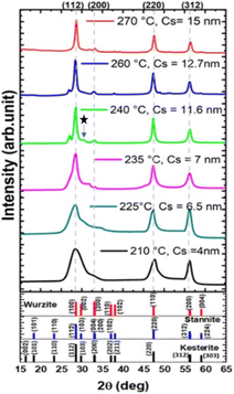
In our synthesis, the precursor solutions were formulated in Cu-poor and Zn-rich environments to create the defects necessary to maximize its p-type semiconductor nature. This Cu-poor and Zn-rich approach has been previously reported to be beneficial for the p-type semiconductor behaviour and to reduce the formation of secondary phases.39,50To gain a deeper understanding of the formation of the as-synthesized CZTS NPs, we investigated different injection temperatures ranging from 210 to 270 °C. The XRD patterns of the CZTS NPs synthesized at these different injection temperatures are presented in Fig. 1. The kesterite phase of CZTS NPs was observed generally across all injection temperatures, with the intensity of diffraction peaks becoming sharper as the injection temperature increased.
At low injection temperatures (below 235 °C), the synthesized CZTS NPs exhibit a broader peak around 2θ = 28.5°, indicating the presence of fine crystallites or a contribution of multiple peaks. On the other hand, at injection temperatures exceeding 235 °C, the XRD patterns displayed diffraction peaks at 2θ = 28.5°, 33°, 47.4° and 56.2°, corresponding to planes (112), (200), (220) and (312) of the kesterite CZTS (DB card number 00-260575), respectively. This observation is in good agreement with previous reports on CZTS NPs with kesterite structure.28,36,51,52
For the samples synthesized at intermediate temperatures (between 235 and 260 °C), additional diffraction peaks were detected at 2θ = 27.25°, 30.82°, and 48.24°, which correspond to the (100), (101), and (110) planes of wurtzite (DB 00-005-0492).43 The presence of these peaks may suggest the coexistence of wurtzite and kesterite structures.42 Notably, as the injection temperatures exceeded 260 °C, no peaks due to wurtzite were observed, suggesting the formation of a pure kesterite CZTS phase (Fig. 1).53,54 From the XRD patterns, the average crystallite size was calculated from the Scherrer's equation:54
 | (1) |
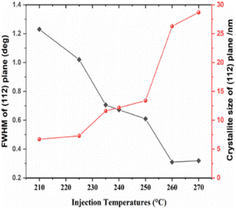 | ||
| Fig. 2 FWHM and crystallite size calculated from the (112) planes of the XRD patterns with respect to different injection temperatures. | ||
The FWHM of the (112) peak was shown to decrease by increasing the injection temperature. Meanwhile, the Cs, determined using the Scherrer equation (eqn (1)), increased from 4 nm at 210 °C to 16 nm at 270 °C, indicating a growth in particle size, as shown in Fig. 1 and 2. This trend is consistent with the previous findings in literature.52,53 Therefore, this indicates that, to achieve the desired pure kesterite phase, the hot injection should be performed at 270 °C. This temperature triggers nucleation and growth of NPs with controlled size.
Secondary phases were not detected in the XRD analysis for the reactions occurred below 235 °C due to the presence of broad peaks. However, in the sample synthesized at 240 °C, a weak diffraction peak located at 2θ = 31° (marked by an asterisk in Fig. 1) was observed, and can be ascribed to SnS traces.1
It is important to note that the purity of CZTS NPs cannot be determined by XRD analysis alone because some secondary phases, such as ZnS, Cu2−xS and Cu2SnS3, have similar XRD patterns to the CZTS phase.
Therefore, Raman spectroscopy was employed as a complementary analysis to XRD with the aim to identify the presence of other secondary phases.
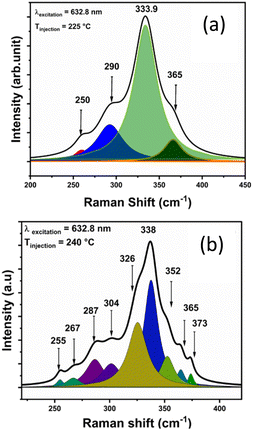
Fig. 3 shows the Raman spectra of the synthesized CZTS NPs, as a function of the injection temperature. For the CZTS NPs synthesized at lower temperatures (210 °C and 225 °C), the most intense Raman vibrational mode (A) is observed at about 333 cm−1. A second peak appears as a broad shoulder at around 290 cm−1. The broadness of the Raman peaks could be ascribed to the NPs size, the presence of a surface capping agent (OLA), and the stresses and strains within the NPs.55,56
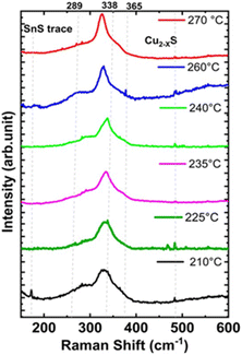 | ||
| Fig. 3 Raman spectra of CZTS NPs (powders) synthesized at a fixed reaction time of 30 minutes for various injection temperatures ranging from 210 °C to 270 °C using hot-injection methods. | ||
The vibrational mode at 290 cm−1 likely corresponds to the mixture of kesterite (vibrational mode A: 285–290 cm−1) and stannite (vibrational mode B – 292 cm−1), as noted in previous studies.55–58 Additionally, a very small peak is seen at around 475 cm−1 for low injection temperatures, which may be associated to Cux−2S. As the injection temperature increases (from 235 to 270 °C), the Cu2−xS (475 cm−1) peak disappears, and the weak Raman mode at 287 cm−1, along with other Raman vibrational modes at 290, 337, and 365 cm−1, become visible, confirming the formation of the kesterite CZTS phase.58 The formation of other secondary phases, including ZnS (352 cm−1) and Cu2SnS3 (355–356 cm−1) was not detected from the Raman spectral analysis.58–60
Peak fitting was performed for the samples synthesized at 225 °C and 240 °C, as shown in Fig. 4a and b, respectively, to verify the presence of by-products alongside with the formation of the CZTS phase. Several deconvoluted peaks associated to CZTS were observed in the sample injected at 240 °C (Fig. 4b), confirming the phase can be assigned to kesterite.58
The FWHM of the main Raman peak decreased with increasing injection temperature in agreement with XRD data, indicating that the crystallinity of the as-synthesized CZTS NPs improves by increasing temperatures, as shown in Fig. 3.
Both XRD and Raman spectra results have confirmed that the injection temperatures above 240 °C give narrower size distributions and higher crystallinity of CZTS materials when compared to those obtained at lower temperatures.61,62 In fact, from a kinetics viewpoint, the ions have a greater reactivity at high temperatures, so facilitating the nucleation and the growth of the NPs.53
Morphological and compositional characterization
The characterization of the crystal structure, chemical composition, and size distribution was carried out by SEM-EDX and TEM, respectively.The SEM images of the CZTS NPs (powder) prepared at different injection temperatures (210 °C to 270 °C) for 30 minutes are shown in Fig. S1 (see ESI).† The NPs synthesized at the temperatures of 210 °C and 225 °C exhibit irregular granular shapes, and they seem to be packed in clusters, as it can be seen in Fig. S1a and b.† On the other hand, the morphology of the NPs synthesized at injection temperatures of 235 °C, 240 °C and 260 °C show a quasi-spherical morphology with a slight increase in size by increasing the injection temperature.63 However, at an elevated injection temperature of 270 °C, NPs exhibited a uniform spherical morphology with good homogeneity throughout their growth.
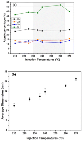
The SEM-EDX analysis of CZTS NPs synthesized at different injection temperatures is shown in Fig. 5a. It is worth noting that, during the quantitative elemental analysis, we exclusively focused on the results obtained from SEM-EDX, since the samples used in the TEM analysis were prepared on a copper grid, which introduces an error on the Cu atomic percentage composition during TEM-EDX analysis. Fig. 5a shows the elements' atomic percentages, which should be 2![[thin space (1/6-em)]](https://www.rsc.org/images/entities/char_2009.gif) :
:![[thin space (1/6-em)]](https://www.rsc.org/images/entities/char_2009.gif) 1
1![[thin space (1/6-em)]](https://www.rsc.org/images/entities/char_2009.gif) :
:![[thin space (1/6-em)]](https://www.rsc.org/images/entities/char_2009.gif) 1
1![[thin space (1/6-em)]](https://www.rsc.org/images/entities/char_2009.gif) :
:![[thin space (1/6-em)]](https://www.rsc.org/images/entities/char_2009.gif) 4, i.e. Cu = 25%, Zn and Sn are 12.5%, and S = 50%. The average chemical compositions of Cu/(Zn + Sn) and Zn/Sn in the CZTS NPs obtained at different injection temperatures are summarized in Table 1.
4, i.e. Cu = 25%, Zn and Sn are 12.5%, and S = 50%. The average chemical compositions of Cu/(Zn + Sn) and Zn/Sn in the CZTS NPs obtained at different injection temperatures are summarized in Table 1.
| Injection temperatures (°C) | Chemical composition ratios | ||
|---|---|---|---|
| Cu/Zn/Sn/S | Cu/(Zn + Sn) | Zn/Sn | |
| 210 | Cu2.1Zn1.2Sn1.0S3.8 | 0.96 | 1.25 |
| 225 | Cu2.3Zn1Sn1.2S4.0 | 1.07 | 0.82 |
| 235 | Cu1.8Zn1.1Sn1S3.2 | 0.87 | 1.08 |
| 240 | Cu1.9Zn1.1Sn1.1S4.1 | 0.92 | 1.10 |
| 260 | Cu2.1Zn1.1Sn1.1S4.19 | 0.96 | 1.16 |
| 270 | Cu1.8Zn1.1Sn1.0S3.26 | 0.86 | 1.15 |
Even though the CZTS NPs were prepared in the copper-poor and zinc-rich condition, we can easily observe that the quantitative elemental analysis of Cu, Zn, Sn and S at an injection temperature of 210 °C, 225 °C, and 270 °C shows a composition that slightly deviates from an ideal stoichiometric value (Fig. 5a). An excess of Cu and Zn has been found in NPs obtained at an injection temperature of 210 °C, which describes a sulphur-poor condition. Thus, at an injection temperature of 210 °C, a slight increase in Cu and Zn can be observed in the NPs, while the S content in the NPs decreases. Moving to the 225 °C injection temperature, the Zn/Sn ratio decreases while the Cu/(Zn + Sn) ratio increases, with a slight increase in the content of both Sn and Zn. These compositional variations can lead to the formation of secondary phases, such as ZnS, SnxSy, Cu2−XS, and Cu2SnS3. The elemental ratios for CZTS NPs prepared at injection temperatures of 240 °C and 260 °C closely match the desired compositional values for CZTS absorbers used in solar cells, suggesting the successful formation of near-stoichiometric CZTS NPs within a temperature range between 240 and 260 °C. This is consistent with previous literature reports.52,64–66
The morphologies of the so-obtained CZTS NPs synthesized at different injection temperatures were characterised through TEM, as shown in Fig. S2.† At injection temperatures of 210 °C, the NPs demonstrate slightly irregular mixed morphology, including a pseudo-spherical-like structure, triangular and hexagonal-like. As the injection temperature increased to 225 °C, the mixed morphology is still detectable (Fig. S2b†). With a further increase of the injection temperature, no mixed morphology was observed, and the NPs appeared to have a quasi-regular spherical-like shape.
The high-resolution TEM image (HR-TEM) in Fig. S2,† along with the corresponding Fast Fourier Transform (FFT, inset) pattern, shows lattice fringes that confirm the good crystallinity quality of the CZTS NPs. These lattice fringes are attributed to the (112) planes of the kesterite CZTS NPs.67 Despite variations in the injection temperatures, the observed lattice fringes suggested that the interplanar spacing (d) remained quasi-identical for all samples: 0.37 nm, 0.31 nm, 0.36 nm, 0.36 nm, 0.34 nm, and 0.36 nm, respectively corresponding to injection temperatures of 210 °C, 225 °C, 235 °C, 240 °C, 260 °C and 270 °C, (see Fig. S2†).
The average diameter of the as-synthesized CZTS NPs, depicted in Fig. 5b, was determined by manually outlining the edges of the NPs in TEM images. Using the software ImageJ, the particles' area was evaluated and then converted to particle dimensions. It was observed that the average size of the NPs increased from 9 to 15 nm as a function of temperature (Fig. 5b). This result strongly suggests that the size of the NPs can be effectively controlled by varying the injection temperatures,56 leading to a direct significant improvement in their performance in various applications. For example, in photovoltaics, smaller NPs can form more uniform and crack-free films, which is essential for improved performance.68,69 In photocatalytic applications, the increased surface area from the smaller particles boosts catalytic activity.6
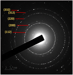
Furthermore, confirmation of the good crystallinity of the CZTS NPs is provided by the selected area electron diffraction (SAED) pattern shown in Fig. 6, which corresponds to the diffraction patterns of the (112), (200), (220), (312) and (332) planes of kesterite CZTS. These results are consistent with the XRD analysis shown in Fig. 1.
Additionally, the STEM elemental nanoscale mapping was conducted to confirm the elemental distribution of the CZTS NPs, as shown in Fig. S3(a–f).† The elemental maps confirmed the homogeneous distribution of all four elements constituting CZTS among the NPs.
Optical characterization
The optical absorption spectra of the as-synthesized CZTS NPs were determined by UV-visible spectroscopy, and the band gap (Eg) was calculated using the Kubelka–Munk function, as shown in eqn (2):
 | (2) |
CZTS is a direct band gap semiconductor material, optical Eg of the CZTS NPs is determined by the linear extrapolation of the plot [F(R)hν]2 versus the photon energy (hν) (Fig. 7a): the Eg ranges between 1.51 eV and 1.54 eV. These variations in Eg are due to variation in the NPs dimension.72
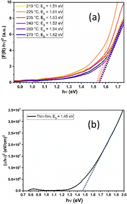 | ||
| Fig. 7 (a) Band gap of CZTS NPs (powder) synthesized at a fixed reaction time of 30 minutes for various injection temperatures ranging from 210 °C to 270 °C and (b) thin-film. | ||
Fig. 7b shows the optical Eg of the CZTS thin film deposited onto soda lime glass. The layer was produced using the CZTS NPs synthesized at the optimized injection temperatures of 240 °C, as already previously described in the experimental section. The Eg has been evaluated to be 1.45 eV, in accordance with the literature on the topic.25,42,71,73
Effect of HCl treatment on Cu2ZnSnS4 nanoparticles
To selectively remove secondary phases such as ZnS, and Cu2SnS3, and other potential by-products, a further purification step involving a properly diluted HCl wash treatment was performed after the synthesis on the CZTS NPs obtained at an optimized injection temperature of 240 °C. A detailed description is provided in the purification section. A proper dilution of HCl has been done to effectively remove the detrimental secondary phases without affecting the synthesised CZTS NPs. The effect of HCl treatment on the compositional profile and crystallinity of the nanostructure was investigated using XRD, EDS and XPS both before and after the HCl washing treatment. Fig. S4† shows the XRD pattern of the CZTS NPs synthesized at 240 °C before (black line) and after (red line) washing with HCl solution (3.7% v/v at 40 °C for 10 minutes). The XRD pattern of the untreated NPs shows clear diffraction peaks at 2θ = 28.2°, 33°, 47.4° and 56.2°, corresponding to the (112), (200), (220), and (312) planes of kesterite CZTS (DB card number 00-260575), respectively, along with additional peaks ascribed to traces of SnS2. In contrast, the XRD pattern for the HCl-treated NPs (red line), shows characteristic peaks for the CZTS phase with no additional peaks, indicating the absence of impurities or secondary phases. Additionally, the FWHM only slightly decreased after HCl treatment, as shown in Table S1,† demonstrating that the HCl washing treatment, when conducted at the proper optimised diluted conditions, selectively removes unwanted by-products without impacting the crystallinity of the CZTS NPs. However, no phases related to ZnS and Cu2SnS3 were detected, as their diffraction peaks are difficult to distinguish from those of the CZTS phase. As an additional confirmation, the compositional profile of CZTS NPs was investigated by EDS analysis, as shown in Fig. S5.†The EDS spectra before and after HCl treatment indicate remarkable changes in elemental composition. The results show the elemental composition of the NPs both untreated and treated with HCl (shown in Fig. S5†). The analysis revealed that the Zn content decreased after HCl treatment, suggesting that ZnS traces were effectively removed. As a consequence, the Cu composition ratio is indirectly increased and the Zn/Sn ratio decreased, likely due the decrease of the Zn concentration. Additionally, treated NPs spectra show the presence of Cl peaks, indicating residual chloride that can be removed by further washing with DI water. Therefore, the HCl washing treatment effectively removes unwanted ZnS, without impacting the crystallinity or crystallite size of NPs and leading to a high purity of the CZTS NPs phase.
X-ray photoelectron spectroscopy (XPS) was further employed to investigate the effect of the HCl washing treatment on other possible by-products. Fig. S6† shows the high resolution XPS spectra for Cu, Zn, Sn, S and Cl before and after the acid treatment. The Cu 2p core-level spectrum, Fig. S6(a),† shows the peaks related to Cu 2p3/2 and Cu 2p1/2 with a peak separation of 19.8 eV and of 19.9 eV respectively before and after the HCl treatment. In both cases, the peak separation value indicates the presence of Cu1+ in the NPs.74 The binding energies of the peaks are reported in Table S2.† Also, the spectrum in Fig. S6(b),† related to Zn 2p, shows the typical peak separation of Zn in the oxidation state +2, of approximately 23.2 eV for both the spectra before and after the acid treatment.74 The scenario gets more complex for the spectra before and after the HCl washing related to Sn, Fig S6(c).† In both cases it is possible to observe a convolution of peaks where each doublet presents a peak separation of about 8.4 eV, Table S2.† However, both before and after treatment, the pairs of peaks at higher energies (487.3 eV and 495.8 eV pre-treatment; 487.3 and 495.7 post-treatment) are related to Sn in +4 oxidation state,75 as expected for the CZTS NPs. While the doublets of peaks at lower energies (486.2 eV and 494.5 eV pre-treatment; 486.3 eV and 494.7 eV post treatment) are due to Sn in +2 oxidation state,75 indicating the presence of some secondary phase, such as SnS which could had not been detected through XRD due to their probable amorphous nature. However, after the HCl treatment, the area of Sn4+ peaks increases while the area of Sn2+ peaks decreases, indicating that with the acid washing some part of the Sn2+-containing by-products are removed. About S 2p, in the spectra both before and post treatment, Fig. S6(d),† it is possible to observe a doublet at low binding energies in the range of 161.0–163.0 eV, which is coherent with the energy range expected for S in sulphide (about 161.0–164.0 eV).74 Here the peak separation is 1.1 eV, as known for S2− valence state. However, the spectrum before the treatment also presents a convolution of peaks around 166.9–170.0 eV, which disappear after the HCl treatment. Sulphur peaks at these binding energies are related to sulphate phases76 and their disappearance indicates the removal of sulphur by-products with the acidic treatment. These results are also confirmed by Table S3,† containing the atomic percentage of S in sulphate phases and in sulphide phases over the total amount of sulphur. The sulphate amount drastically decreases with the acid treatment. Fig. S6(e)† confirms the presence of Cl in the treated NPs spectrum, however also in this case the residual chloride can be removed by further washing the NPs powder with DI water. Additionally, XPS also detected organic nitrogen peaks at 400.0 (amine) & 401.8 eV (quaternary amine) (Fig. S7b†), which would be consistent with the presence of a nitrogen containing surfactant such as OLA. This nitrogen signal drops considerably from 1.61 at% to 0.33 at% after the HCl treatment, with surface carbon also reducing on the HCl treatment (Table S3†).
To investigate possible effects of the HCl washing treatment on the band structure of the CZTS NPs, Ultraviolet photoelectron spectroscopy (UPS) was employed. Notably, with this technique it is possible to extrapolate the work function (WF), the valence band (VB) and the ionizing potential (IP) of the CZTS NPs.77,78 The obtained values are reported in Table S4.† and remain stable after the HCl treatment.
Infrared spectroscopy (FT-IR) analysis
As detailed in the upcoming experimental section, CZTS NPs were prepared using the hot-injection method with OLA (C18H35NH2) as a solvent and a capping agent. It is worth mentioning that OLA is one of the most widely used surfactants in the colloidal synthesis of nanostructures.79 It is used to control the growth of NPs in the desired shape and size and to prevent the NPs aggregation through steric stabilization thanks to the presence of the bulky organic chain ligands.30,79–81 However, these long-chain organic ligands might be challenging to be removed entirely from the NPs surface. These organic residues can limit their functionality in optoelectronics, photocatalysis, and photovoltaics since they hinder the electrical conductivity or photocatalytic properties.80 Several methods have been developed to avoid these problems, such as the ligand-exchange approaches, in which a new ligand with a short organic chain replaces the original clunky ligand.80–83 Although the ligand-exchange approach is a powerful method for modifying the surface and properties of NPs, retaining the original size and shape is challenging.84 Therefore, finding an alternative path that allows the OLA residues removal and leaves the CZTS NPs unchanged is urgent.The here proposed chemical treatment with HCl solutions has proved to be decisive: it was beneficial not only to remove the possible by-products formed during the CZTS NPs growth but also to remove additional organic ligands from the NPs surface without changing their original shape and size. Remarkably, the presence of OLA on the surface of the CZTS NPs disappeared through washing with HCl treatment, which is consistent with XPS results (Table S3†).
The purity (the absence of these capping ligands) of the CZTS NPs (powder) was assessed by ATR-FTIR spectroscopy.
Fig. 8 shows the ATR-FTIR spectra of pure OLA (black spectrum) and untreated and HCl-treated CZTS NPs. FTIR spectrum of untreated CZTS NPs clearly confirms the presence of OLA on CZTS surface: in fact, the spectrum shows the characteristic bending vibration mode of C–N (δC–N) group of at ∼1071 cm−1, the bending vibration related to N–H groups (δN–H) at 1590 cm−1 and the stretching vibration of C![[double bond, length as m-dash]](https://www.rsc.org/images/entities/char_e001.gif) C groups (νC
C groups (νC![[double bond, length as m-dash]](https://www.rsc.org/images/entities/char_e001.gif) C) at 1647 cm−1.79 Besides, the asymmetric stretching (νas) and the symmetric stretching (νs) vibrations of the C–H bonds in the CH2 groups, located at 2922 and 2854 cm−1 respectively for pure OLA, were observed to shift to lower wavenumbers. This is due to the limitation of C–H motions due to the coordination on the NPs surface.66,79 On the other hand, in the CZTS NPs treated with HCl, the characteristic vibrational mode assigned to OLA gradually disappears, as shown in Fig. 8. Interestingly, after a second wash with HCl treatment, OLA carbon foot print is no longer observed, providing evidence that HCl treatments successfully remove the residual organic ligand from the NPs surfaces.
C) at 1647 cm−1.79 Besides, the asymmetric stretching (νas) and the symmetric stretching (νs) vibrations of the C–H bonds in the CH2 groups, located at 2922 and 2854 cm−1 respectively for pure OLA, were observed to shift to lower wavenumbers. This is due to the limitation of C–H motions due to the coordination on the NPs surface.66,79 On the other hand, in the CZTS NPs treated with HCl, the characteristic vibrational mode assigned to OLA gradually disappears, as shown in Fig. 8. Interestingly, after a second wash with HCl treatment, OLA carbon foot print is no longer observed, providing evidence that HCl treatments successfully remove the residual organic ligand from the NPs surfaces.
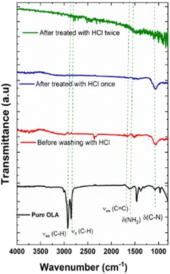 | ||
| Fig. 8 FTIR-ATR spectrum of pure OLA spectrum and CZTS NPs at 240 °C for 30 minutes: before washing with HCl (red spectrum) and after washing with HCl (blue and green spectrum). | ||
Thermogravimetric analysis
Fig. 9 shows the TGA of CZTS NPs synthesized at 240 °C (30 minutes). TGA was performed by heating the CZTS NPs from 30 to 550 °C, because the process temperatures to produce the CZTS materials does not normally exceed 550 °C. The weight loss profile as a function of temperature for the CZTS NPs, untreated and HCl-treated, is shown in Fig. 9. Below 100 °C, the TGA curve shows a weight loss of about 10% for the untreated CZTS NPs, which is attributed to moisture loss, and/or residual solvents from purification steps. It is noteworthy that, in the range 100–550 °C, a weight loss of about 22% was observed for the untreated CZTS NPs and this can be mainly attributed to the removal of residual organic traces, specifically to the removal of OLA capped onto the surface of the CZTS NPs. On the other hand, HCl-treated CZTS NPs, showed a modest weight loss of about 6.5% over the entire temperature, thus confirming the almost complete removal of residual OLA from CZTS NPs.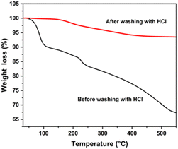 | ||
| Fig. 9 TGA spectrum of CZTS NPs synthesized at 240 °C for 30 minutes: before washing with HCl (black spectrum) and after washing with HCl (red). | ||
Furthermore, the TGA measurement can provide valuable information about the weight loss behaviour of CZTS NPs, including some secondary phases within the temperature range between 300 and 450 °C, comprising ZnS, SnS2, Cu2SnS3, and Cu2−xS, which can undergo significant decomposition in this regime.81 Therefore, the highest mass loss indicated in the untreated CZTS NPs may be not univocally associated to the thermal decomposition of bulky hydrocarbon chain molecules, but it might also be due to a weight loss related to the decomposition of some detrimental phases.81 These mass losses are negligible in the HCl-treated NPs (see Fig. 9, red spectrum). These results underline the multifaceted utilisation of HCl treatment as an effective strategy for the removal of both organic residues and detrimental phases without compromising the original size and shape of the NPs. These findings could facilitate the application of CZTS NPs in optoelectronics and photocatalysis.
Conclusion
In this study, CZTS NPs were successfully synthesized by utilizing the hot injection method with OLA as both solvent and capping agent. The study of various injection temperatures, while maintaining a fixed reaction time of 30 minutes, showed a significant impact on the crystal growth of CZTS NPs. We found that an injection temperature lower than 235 °C resulted in the formation of secondary phases, as confirmed by Raman and XRD analysis. Conversely, injection temperatures higher than 240 °C led to high-quality NPs. The EDX analysis confirmed that the injection temperatures required to achieve the desired chemical composition of the CZTS NPs range between 240 and 270 °C. Additionally, we demonstrated a successful strategy employing HCl washing treatment to remove secondary phases and the organic traces. This treatment facilitated the growth of the predominantly pure CZTS phase. In general, the findings reported herein contribute to understand and control the CZTS NPs synthesis and purification processes, paving the way for their applications in photovoltaics, photocatalysis and beyond.Experimental
Chemical reagents
All chemical reagents used in this work were purchased from Sigma Aldrich Corporation (St. Louis, MO, USA) and used without any further purification: copper(II) acetate monohydrate (Cu(CH3COO)2·H2O, >99%), zinc(II) acetate dihydrate (Zn(CH3COO)2·2H2O, 99.99%), sulphur powder (>99.5%), tin(II) chloride dihydrate (SnCl2·2H2O, >98%), oleylamine (OLA, 98%), hydrochloric acid (HCl, 37%), toluene (99.8%), p-xylene (>99.7%), and ethanol (C2H6O, >99%). Deionized (DI) water was produced by a Milli-Q Essential.Synthesis of Cu2ZnSnS4 nanoparticles
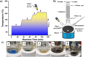
In this study, CZTS NPs were synthesized using an optimized hot injection technique based on the method described elsewhere with slight modifications.85,86 Two solutions were prepared for the synthesis process: (i) a first solution (SOL-A) containing all metal precursors, by dissolving in a three-neck flask, Cu(CH3COO)2·H2O (3.68 mmol), SnCl2·2H2O (1.85 mmol), and Zn(CH3COO)2·2H2O (2.0 mmol) in OLA (20.0 mL) in this order; (ii) a second solution (SOL-B) containing elemental sulphur powder (8.03 mmol) in OLA (10.0 mL). Both mixtures were connected to a vacuum/N2 Schlenk line and vacuumed separately. SOL-B was degassed for 1 h at 60 °C under constant stirring. At the same time, SOL-A was subjected to a four-step temperature process, as shown in Fig. 10a. First, SOL-A was degassed at 100 °C under a vigorous stirring for 30 minutes to remove the dissolved oxygen and unwanted moisture (step 1). The flask was then filled with N2 atmosphere as depicted in Fig. 10b, the temperature was raised to 150 °C, and the mixture was kept at this temperature for 30 minutes (step 2). Later, the temperature was increased to 190 °C and held for 10 minutes (step 3) while the mixture colour quickly turned from a bluish to yellowish (as shown in Fig. 10c). After this stage, the temperature was continuously raised to the desired injection temperature (in the range 210–270 °C, as explained in the Results and Discussion), and finally SOL-B was rapidly injected into the SOL-A flask. After the injection, the reaction mixture immediately changed the colour from pale yellow to dark brown (step 4), as shown in Fig. 10c. Subsequently, the system was left to react at the injection temperature for 30 minutes (step 4). The flask was finally removed from the heating mantle and cooled naturally to room temperature in an inert atmosphere.Purification of Cu2ZnSnS4 nanoparticles
The aim of the purification step is to selectively remove the by-products (secondary phases) and the excess of organic ligand residues from the surface of the NPs. These organic residues can significantly influence the structural and optical properties during characterization. The purification procedure for the freshly synthesized NPs-OLA solution is as follows: first, the obtained NPs-OLA product was washed with a mixture of chloroform and ethanol (in a ratio of 1/5 v/v) and then centrifuged at 8000 rpm for 2 minutes. The orange supernatant (sulphur/OLA solution) was removed, while the dark precipitate (from now on “untreated NPs”) was dispersed in a 3.7% v/v HCl solution in water and then magnetically stirred at 40 °C for 10 minutes. Subsequently, the NPs were isolated again by centrifugation. The last two steps were repeated twice to ensure thorough purification. The so-obtained dark precipitate was then washed several times with DI water to remove HCl residues. Finally, the resulting black coloured NPs were collected by centrifugation (from now on “treated NPs”). Both (untreated and treated with HCl) NPs underwent the following final steps: half of each production batch was dried under vacuum and stored under N2 atmosphere to preserve the NPs properties for further characterization. The other half was dispersed in p-xylene to produce inks with concentrations of 200 mg mL−1. The so-obtained suspension underwent sonication to achieve a uniform and homogeneous ink which was used to deposit thin films of CZTS NPs onto soda-lime glass substrate by spin-coating at 4000 rpm for 30 seconds, followed by annealing at 100 °C for 10 minutes on a hot-plate in ambient air to remove the solvent. The purification details are summarized in the Fig. S8 (please see ESI).†CZTS NPs powder and film characterization
The material's structure was investigated by X-ray diffraction (XRD) using a Rigaku Miniflex 600 device (FF tube 40 kV, 15 mA, using CuKα radiations at λ = 1.5405 Å) and Raman spectroscopy (RS), by the Jasco Ventuno μ-Raman instrument at a wavelength of 632.8 nm, power density 6 kW cm−2. Scanning electron microscopy-energy dispersive X-ray analysis (SEM-EDX) was performed using the Tescan VEGA TS5136XM. Absorbance spectra measurements were achieved using the Jasco V-570 UV-Visible spectrophotometer. Transmission electron microscopy (TEM) investigations were carried out on a JEOL JEM-2100PLUS with an emission voltage of 200 kV. Samples were prepared by dropping a diluted solution of 0.05 mg mL−1 on a Cu grid.X-ray photoelectron spectroscopy (XPS) analysis was carried out on a Kratos Axis Supra with a monochromated Al Kα source at 225 W (15 kV, 20 mA). Charge calibration was to the C–C peak at 284.8 eV and charge neutralization was not required. High resolution spectra at 40 eV pass energy, 1 s dwell time, and typically 5 sweeps, were collected for all elements based on a survey scan at 160 eV pass energy. Ultraviolet photoelectron spectroscopy (UPS) was carried out on the Kratos Axis Supra using the He(I) line and the electrons collected at a 10 eV pass energy, with the 55 μm aperture to protect the detector. XPS & UPS data were analysed in CasaXPS 2.3.24PR1.0 using the Kratos relative sensitivity factors. The valence band maximum and secondary electron cutoff (work function) in UPS were modelled using the “Step Down” and “Step Up” region options to ascertain the intercept with the x-axis. Infrared spectroscopy (FT-IR) measurements were carried out using a JASCO FTIR-4100 with an attenuated total reflectance (ATR) accessory (ZnSe crystal) in the region from 600 to 4000 cm−1 with a resolution of 1 cm−1 in air. Thermogravimetric Analysis (TGA) were performed by means of a Mettler Toledo TGA/DSC1 STARe system (30–550 °C temperature range, 10 °C min−1 heating rate, constant nitrogen flow of 50 mLmin−1).
Data availability
All data have been presented in the work.Author contributions
Amin Hasan Husien: writing – original draft, data curation; visualization; formal analysis; investigation; writing – review & editing; Giorgio Tseberlidis: conceptualization, investigation, methodology, supervision, project administration, writing – review & editing; Vanira Trifiletti: data curation, formal analysis, supervision, validation, visualization, writing – original draft, writing – review & editing; Elisa Fabbretti: data curation, investigation & methodology; Silvia Mostoni: formal analysis; James Mcgettrick: validation, investigation & methodology, data curation, formal analysis; Riccardo Po: conceptualization, project administration, resources, supervision; Simona Binetti: conceptualization, project administration, resources, supervision.Conflicts of interest
There are no conflicts to declare.Acknowledgements
AHH acknowledges a PhD scholarship on Green Issues from action IV.5 of the PON Research and Innovation 2014–2020 “Education and research for recovery – REACT-EU” program. This work has been also partially supported by the research project [CANVAS-Nuovi Concetti, materiali e tecnologie per l'integrazione del fotovoltaico negli edifici in uno scenario di generazione diffusa], funded by the Italian Ministry of the Environment and the Energy Security, through the Research Fund for the Italian Electrical System [type-A call, published on GURI no. 192 on 18-08-507 2022]. EF, JMcG & TW acknowledge the VIPERLAB project funded by the European Union's Horizon 2020 research and innovation programme under grant agreement no. 101006715.Notes and references
- G. Tseberlidis, V. Trifiletti, A. Le Donne, L. Frioni, M. Acciarri and S. Binetti, Sol. Energy, 2020, 208, 532–538 CrossRef CAS.
- M. Nakamura, K. Yamaguchi, Y. Kimoto, Y. Yasaki, T. Kato and H. Sugimoto, IEEE J. Photovoltaics, 2019, 9, 1863–1867 Search PubMed.
- M. He, C. Yan, J. Li, M. P. Suryawanshi, J. Kim, M. A. Green and X. Hao, Adv. Sci., 2021, 8, 2004313 CrossRef CAS PubMed.
- A. Le Donne, V. Trifiletti and S. Binetti, Front. Chem., 2019, 7, 297 CrossRef CAS PubMed.
- S. A. Phaltane, S. A. Vanalakar, T. S. Bhat, P. S. Patil, S. D. Sartale and L. D. Kadam, J. Mater. Sci.: Mater. Electron., 2017, 28, 8186–8191 CrossRef CAS.
- X. Hou, Y. Li, J.-J. Yan and C.-W. Wang, Mater. Res. Bull., 2014, 60, 628–633 CrossRef CAS.
- M. Burhanuz Zaman, R. A. Mir and R. Poolla, Int. J. Hydrogen Energy, 2019, 44, 23023–23033 CrossRef CAS.
- X.-L. Zheng, Y.-J. Yang, Y.-H. Liu, P.-L. Deng, J. Li, W.-F. Liu, P. Rao, C.-M. Jia, W. Huang, Y.-L. Du, Y.-J. Shen and X.-L. Tian, Rare Met., 2022, 41, 2153–2168 CrossRef CAS.
- G. Tseberlidis, V. Trifiletti, A. H. Husien, A. L’Altrella, S. Binetti and F. Gosetti, Appl. Sci., 2024, 14, 9923 CrossRef CAS.
- E. V. Maistruk, I. P. Koziarskyi, D. P. Koziarskyi, P. D. Marianchuk and V. V. Brus, Proc. SPIE, 2018, 10612, 1061215 Search PubMed.
- F. Liu, K. Zhang, Y. Lai, J. Li, Z. Zhang and Y. Liu, Electrochem. Solid-State Lett., 2010, 13, H379 CrossRef CAS.
- V. Trifiletti, L. Frioni, G. Tseberlidis, E. Vitiello, M. Danilson, M. Grossberg, M. Acciarri, S. Binetti and S. Marchionna, Sol. Energy Mater. Sol. Cells, 2023, 254, 112247 CrossRef CAS.
- A. V. Moholkar, S. S. Shinde, A. R. Babar, K.-U. Sim, Y. Kwon, K. Y. Rajpure, P. S. Patil, C. H. Bhosale and J. H. Kim, Sol. Energy, 2011, 85, 1354–1363 CrossRef CAS.
- E. Garcia-Llamas, J. M. Merino, R. Gunder, K. Neldner, D. Greiner, A. Steigert, S. Giraldo, V. Izquierdo-Roca, E. Saucedo, M. León, S. Schorr and R. Caballero, Sol. Energy, 2017, 141, 236–241 CrossRef CAS.
- W. Wang, M. T. Winkler, O. Gunawan, T. Gokmen, T. K. Todorov, Y. Zhu and D. B. Mitzi, Adv. Energy Mater., 2014, 4, 1301465 CrossRef.
- M. Sahu, V. R. M. Reddy, B. Kim, B. Patro, C. Park, W. K. Kim and P. Sharma, Materials, 2022, 15, 1–16 CrossRef PubMed.
- M. Y. Yeh, C. C. Lee and D. S. Wuu, J. Sol-Gel Sci. Technol., 2009, 52, 65–68 CrossRef CAS.
- G. Tseberlidis, A. Hasan Husien, S. Riva, L. Frioni, A. Le Donne, M. Acciarri and S. Binetti, Sol. Energy, 2021, 224, 134–141 CrossRef CAS.
- V. Trifiletti, S. Mostoni, F. Butrichi, M. Acciarri, S. Binetti and R. Scotti, ChemistrySelect, 2019, 4, 4905–4912 CrossRef CAS.
- F. Butrichi, V. Trifiletti, G. Tseberlidis, B. E. G. Colombo, F. Taglietti, M. Rancan, L. Armelao and S. Binetti, Sol. Energy Mater. Sol. Cells, 2024, 272, 112924 CrossRef CAS.
- G. Tseberlidis, V. Trifiletti, E. Vitiello, A. H. Husien, L. Frioni, M. Da Lisca, J. Alvarez, M. Acciarri and S. O. Binetti, ACS Omega, 2022, 7, 23445–23456 CrossRef CAS PubMed.
- V. Trifiletti, G. Tseberlidis, M. Colombo, A. Spinardi, S. Luong, M. Danilson, M. Grossberg, O. Fenwick and S. Binetti, Materials, 2020, 13, 1471 CrossRef CAS PubMed.
- N. Nakayama and K. Ito, Appl. Surf. Sci., 1996, 92, 171–175 CrossRef CAS.
- Q. Luo, Y. Zeng, L. Chen and C. Ma, Chem.–Asian J., 2014, 9, 2309–2316 CrossRef CAS PubMed.
- R. Aruna-Devi, M. Latha, S. Velumani and J. Á. Chávez-Carvayar, Rare Met., 2021, 40, 2602–2609 CrossRef CAS.
- Q. Guo, H. W. Hillhouse and R. Agrawal, J. Am. Chem. Soc., 2009, 131, 11672–11673 CrossRef CAS PubMed.
- Q. Guo, G. M. Ford, W.-C. Yang, B. C. Walker, E. A. Stach, H. W. Hillhouse and R. Agrawal, J. Am. Chem. Soc., 2010, 132, 17384–17386 CrossRef CAS PubMed.
- S. Jain, P. Chawla, S. N. Sharma, D. Singh and N. Vijayan, Superlattices Microstruct., 2018, 119, 59–71 CrossRef CAS.
- D. Xia, P. Lei, Y. Zheng and B. Zhou, J. Mater. Sci.: Mater. Electron., 2015, 26, 5426–5432 CrossRef CAS.
- U. Ghorpade, M. Suryawanshi, S. W. Shin, K. Gurav, P. Patil, S. Pawar, C. W. Hong, J. H. Kim and S. Kolekar, Chem. Commun., 2014, 50, 11258 RSC.
- M. Zhou, Y. Gong, J. Xu, G. Fang, Q. Xu and J. Dong, J. Alloys Compd., 2013, 574, 272–277 CrossRef CAS.
- S. E. Habas, H. A. S. Platt, M. F. A. M. van Hest and D. S. Ginley, Chem. Rev., 2010, 110, 6571–6594 CrossRef CAS PubMed.
- J. Perelaer and U. S. Schubert, J. Mater. Res., 2013, 28, 564–573 CrossRef CAS.
- C. Rein, S. Engberg and J. W. Andreasen, J. Alloys Compd., 2019, 787, 63–71 CrossRef CAS.
- C. Coughlan, M. Ibáñez, O. Dobrozhan, A. Singh, A. Cabot and K. M. Ryan, Chem. Rev., 2017, 117, 5865–6109 CrossRef CAS PubMed.
- S. C. Riha, B. A. Parkinson and A. L. Prieto, J. Am. Chem. Soc., 2009, 131, 12054–12055 CrossRef CAS PubMed.
- A. K. Soni, R. Joshi and R. S. Ningthoujam, in Handbook on Synthesis Strategies for Advanced Materials: Volume-I: Techniques and Fundamentals, ed. A. K. Tyagi and R. S. Ningthoujam, Springer Singapore, Singapore, 2021, pp. 383–434 Search PubMed.
- K. P. Stroh, M. Szablewski and D. P. Halliday, Mater. Adv., 2024, 5, 1045–1055 RSC.
- M. Kumar, A. Dubey, N. Adhikari, S. Venkatesan and Q. Qiao, Energy Environ. Sci., 2015, 8, 3134–3159 RSC.
- S. Engberg, J. Symonowicz, J. Schou, S. Canulescu and K. M. Ø. Jensen, ACS Omega, 2020, 5, 10501–10509 CrossRef CAS PubMed.
- G. Altamura and J. Vidal, Chem. Mater., 2016, 28, 3540–3563 CrossRef CAS.
- A. Méndez-López, A. Morales-Acevedo, Y. J. Acosta-Silva and M. Ortega-López, J. Nanomater., 2016, 2016, 7486094 Search PubMed.
- G. Agarwal and B. Tripathi, Mater. Today: Proc., 2021, 38, 1229–1232 CAS.
- M. Buffière, G. Brammertz, S. Sahayaraj, M. Batuk, S. Khelifi, D. Mangin, A.-A. El Mel, L. Arzel, J. Hadermann, M. Meuris and J. Poortmans, ACS Appl. Mater. Interfaces, 2015, 7, 14690–14698 CrossRef PubMed.
- K. Kaur, M. Sood, N. Kumar, H. H. Nazari, G. S. Gudavalli, T. P. Dhakal and M. Kumar, Sol. Energy Mater. Sol. Cells, 2018, 179, 22–30 CrossRef CAS.
- Y. Hashimoto, N. Kohara, T. Negami, M. N. Mikihiko Nishitani and T. W. Takahiro Wada, Jpn. J. Appl. Phys., 1996, 35, 4760 CrossRef CAS.
- M. Mousel, A. Redinger, R. Djemour, M. Arasimowicz, N. Valle, P. Dale and S. Siebentritt, Thin Solid Films, 2013, 535, 83–87 CrossRef CAS.
- A. Fairbrother, E. García-Hemme, V. Izquierdo-Roca, X. Fontané, F. A. Pulgarín-Agudelo, O. Vigil-Galán, A. Pérez-Rodríguez and E. Saucedo, J. Am. Chem. Soc., 2012, 134, 8018–8021 CrossRef CAS PubMed.
- N. Kattan, B. Hou, D. J. Fermín and D. Cherns, Appl. Mater. Today, 2015, 1, 52–59 CrossRef.
- J. He, X. Lu, X. Li, Y. Dong, F. Yue, Y. Chen, L. Sun, P. Yang and J. Chu, Sol. Energy, 2018, 159, 572–578 CrossRef CAS.
- E. M. Mkawi, Y. Al-Hadeethi, E. Shalaan and E. Bekyarova, Appl. Phys. A, 2019, 126, 50 CrossRef.
- A. Irkhina, S. Levcenko, V. Hinrichs, P. Plate and T. Unold, RSC Adv., 2017, 7, 11752–11760 RSC.
- H. Zhou, H.-S. Duan, W. Yang, Q. Chen, C.-J. Hsu, W.-C. Hsu, C.-C. Chen and Y. Yang, Energy Environ. Sci., 2014, 7, 998 RSC.
- S. Mustapha, M. M. Ndamitso, A. S. Abdulkareem, J. O. Tijani, D. T. Shuaib, A. K. Mohammed and A. Sumaila, Adv. Nat. Sci.: Nanosci. Nanotechnol., 2019, 10, 045013 Search PubMed.
- R. Ahmad, M. Brandl, M. Distaso, P. Herre, E. Spiecker, R. Hock and W. Peukert, CrystEngComm, 2015, 17, 6972–6984 RSC.
- Y. Qu, G. Zoppi, R. W. Miles and N. S. Beattie, Mater. Res. Express, 2014, 1, 045040 CrossRef CAS.
- K. Ito, Copper Zinc Tin Sulfide-Based Thin Film Solar Cells, John Wiley & Sons, 2014 Search PubMed.
- P. A. Fernandes, P. M. P. Salomé and A. F. da Cunha, J. Alloys Compd., 2011, 509, 7600–7606 CrossRef CAS.
- J. M. R. Tan, Y. H. Lee, S. Pedireddy, T. Baikie, X. Y. Ling and L. H. Wong, J. Am. Chem. Soc., 2014, 136, 6684–6692 CrossRef CAS PubMed.
- A. C. Lokhande, K. V. Gurav, E. Jo, M. He, C. D. Lokhande and J. H. Kim, Opt. Mater., 2016, 54, 207–216 CrossRef CAS.
- H. Zhou, W.-C. Hsu, H.-S. Duan, B. Bob, W. Yang, T.-B. Song, C.-J. Hsu and Y. Yang, Energy Environ. Sci., 2013, 6, 2822 RSC.
- B. Zhou, D. Xia and Y. Wang, RSC Adv., 2015, 5, 70117–70126 RSC.
- B. D. Chernomordik, A. E. Béland, N. D. Trejo, A. A. Gunawan, D. D. Deng, K. A. Mkhoyan and E. S. Aydil, J. Mater. Chem. A, 2014, 2, 10389–10395 RSC.
- H. Cai, L. Yao, Y. Xia, C. Dao, J. Li, L. Lin, Z. Huang and G. Chen, Sol. Energy, 2019, 193, 986–991 CrossRef CAS.
- X. Zhang, E. Fu, Y. Wang and C. Zhang, Nanomaterials, 2019, 9, 336 CrossRef CAS PubMed.
- R. Ahmad, N.-H. Saddiqi, M. Wu, M. Prato, E. Spiecker, W. Peukert and M. Distaso, Inorg. Chem., 2020, 59, 1973–1984 CrossRef CAS PubMed.
- V. T. Tiong, Y. Zhang, J. Bell and H. Wang, CrystEngComm, 2014, 16, 4306–4313 RSC.
- Q. Wu, C. Xue, Y. Li, P. Zhou, W. Liu, J. Zhu, S. Dai, C. Zhu and S. Yang, ACS Appl. Mater. Interfaces, 2015, 7, 28466–28473 CrossRef CAS PubMed.
- V. Foncrose, J. Persello, P. Puech, J. Y. Chane-Ching, D. Lagarde, A. Balocchi and X. Marie, Nanotechnology, 2017, 28, 445709 CrossRef PubMed.
- V. Barron and J. Torrent, J. Soil Sci., 1986, 37, 499–510 CrossRef CAS.
- A. Wei, Z. Yan, Y. Zhao, M. Zhuang and J. Liu, Int. J. Hydrogen Energy, 2015, 40, 797–805 CrossRef CAS.
- W. C. Liu, B. L. Guo, X. S. Wu, F. M. Zhang, C. L. Mak and K. H. Wong, J. Mater. Chem. A, 2013, 1, 3182 RSC.
- C. Imla Mary, S. Ananthakumar, M. Senthilkumar and S. Moorthy Babu, Mater. Today: Proc., 2017, 4, 12484–12490 Search PubMed.
- S. A. Vanalakar, A. S. Kamble, S. W. Shin, S. S. Mali, G. L. Agawane, V. L. Patil, J. Y. Kim, P. S. Patil and J. H. Kim, Sol. Energy, 2015, 122, 1146–1153 CrossRef CAS.
- M. Choi, W. William, J. Hwang, D. Yoon and J. Kim, J. Ind. Eng. Chem., 2018, 59, 160–168 CrossRef CAS.
- J. F. Moulder, W. F. Stickle, P.E. Sobol, K. D. Bomben, Handbook of X-Ray Photoelectron Spectroscopy, ed. J. Chastain, Perkin-Elmer Corporation, 1992, vol. 40 Search PubMed.
- R. Pandiyan, Z. Oulad Elhmaidi, Z. Sekkat, M. Abd-lefdil and M. A. El Khakani, Appl. Surf. Sci., 2017, 396, 1562–1570 CrossRef CAS.
- O. Stroyuk, A. Raevskaya, O. Selyshchev, V. Dzhagan, N. Gaponik, D. R. T. Zahn and A. Eychmüller, Sci. Rep., 2018, 8, 13677 CrossRef PubMed.
- S. Mourdikoudis and L. M. Liz-Marzán, Chem. Mater., 2013, 25, 1465–1476 CrossRef CAS.
- A. Carrete, A. Shavel, X. Fontané, J. Montserrat, J. Fan, M. Ibáñez, E. Saucedo, A. Pérez-Rodríguez and A. Cabot, J. Am. Chem. Soc., 2013, 135, 15982–15985 CrossRef CAS PubMed.
- C. I. Mary, M. Senthilkumar, G. Manobalaji and S. M. Babu, J. Mater. Sci.: Mater. Electron., 2020, 31, 18164–18174 CrossRef.
- H. Zhang, B. Hu, L. Sun, R. Hovden, F. W. Wise, D. A. Muller and R. D. Robinson, Nano Lett., 2011, 11, 5356–5361 CrossRef CAS PubMed.
- C. H. M. van Oversteeg, F. E. Oropeza, J. P. Hofmann, E. J. M. Hensen, P. E. de Jongh and C. de Mello Donega, Chem. Mater., 2019, 31, 541–552 CrossRef CAS PubMed.
- Y. Wang and T. Bürgi, Nanoscale Adv., 2021, 3, 2710–2727 RSC.
- C. Steinhagen, M. G. Panthani, V. Akhavan, B. Goodfellow, B. Koo and B. A. Korgel, J. Am. Chem. Soc., 2009, 131, 12554–12555 CrossRef CAS PubMed.
- L. S. Khanzada, I. Levchuk, Y. Hou, H. Azimi, A. Osvet, R. Ahmad, M. Brandl, P. Herre, M. Distaso, R. Hock, W. Peukert, M. Batentschuk and C. J. Brabec, Adv. Funct. Mater., 2016, 26, 8300–8306 CrossRef CAS.
Footnote |
| † Electronic supplementary information (ESI) available. See DOI: https://doi.org/10.1039/d4na00843j |
| This journal is © The Royal Society of Chemistry 2024 |

