Orientation and morphology control in acid-catalyzed covalent organic framework thin films†
Dayanni D.
Bhagwandin
 ab,
Kirt A.
Page
 abc,
Ly D.
Tran
ab,
Yao
Yao
d,
Alexander
Reidell
 ab,
Christopher
Muratore
e,
Qiyi
Fang
fg,
Aleksey
Ruditskiy
ab,
Cheri M.
Hampton
ab,
Christopher
Muratore
e,
Qiyi
Fang
fg,
Aleksey
Ruditskiy
ab,
Cheri M.
Hampton
 ab,
W. Joshua
Kennedy
 a,
Lawrence F.
Drummy
a,
Yu
Zhong
g,
Tobin J.
Marks
a,
Lawrence F.
Drummy
a,
Yu
Zhong
g,
Tobin J.
Marks
 d,
Antonio
Facchetti
 dh,
Jun
Lou
 f,
Hilmar
Koerner
a,
Luke A.
Baldwin
 a and
Nicholas R.
Glavin
 *a
*a
aMaterials and Manufacturing Directorate, Air Force Research Laboratory, Wright-Patterson Air Force Base, Ohio 45433, USA. E-mail: Nicholas.Glavin.1@us.af.mil
bUES, Inc., Beavercreek, Ohio 45432, USA
cCornell High Energy Synchrotron Source, Cornell University, Ithaca, New York 14853, USA
dDepartment of Chemistry and the Materials Research Center, Northwestern University, Sheridan Road, Evanston, IL 60208, USA
eDepartment of Chemical and Materials Engineering, University of Dayton, Dayton, Ohio 45469, USA
fDepartment of Materials Science and NanoEngineering, Rice University, Houston, Texas 77005, USA
gDepartment of Materials Science and Engineering, Cornell University, Ithaca, New York 14853, USA
hSchool of Materials Science and Engineering, Georgia Institute of Technology, Atlanta, Georgia 30332, USA
First published on 21st March 2024
Abstract
As thin films of semiconducting covalent organic frameworks (COFs) are demonstrating utility for ambipolar electronics, channel materials in organic electrochemical transistors (OECTs), and broadband photodetectors, control and modulation of their thin film properties is paramount. In this work, an interfacial growth technique is utilized to synthesize imine TAPB-PDA COF films at both the liquid–liquid interface as well as at the liquid–solid interface on a Si/SiO2 substrate. The concentration of acetic acid catalyst in the aqueous phase is shown to significantly influence the thin film morphology of the liquid–solid growth, with concentrations below 1 M resulting in no film nucleation, concentrations of 1–4 M enabling smooth film formation, and concentrations greater than 4 M resulting in films with a higher density of particulates on the surface. Importantly, while the films grown at the liquid–liquid interface are mixed-orientation, those grown directly at the liquid–solid interface on the Si/SiO2 surface have highly oriented COF layers aligned parallel to the substrate surface. Moreover, this liquid–solid growth process affords TAPB-PDA COF thin films with p-type charge transport having a transconductance of 10 μS at a gate voltage of −0.9 V in an OECT device structure.
Introduction
Covalent organic frameworks (COFs) are an extraordinarily versatile class of organic materials exhibiting nanoscale porosity, large-scale crystallographic ordering, and offering a vast library of prospective monomers and linker chemistries.1–3 The synthesis of these materials is most commonly performed using solvothermal techniques to generate highly crystalline powders. However, in applications requiring thin films, the fine control of thickness, morphology, crystallographic orientation, composition and structure is necessary to drive the desired properties of interest.4,5 Current approaches towards obtaining high-quality COF thin films directly on solid substrates include bottom-up methods such as solvothermal synthesis,6–23 vapor-assisted conversion,24 and continuous flow.25–27 These bottom-up growth techniques are many times referred to as interfacial synthesis, where monomers are forced to react at liquid–liquid, liquid–solid, or liquid–air interfaces resulting in large grain sizes (micron-scale in some cases)28 and some degree of controllable film thicknesses.29–31 COF thin films synthesized using these methods typically result in films with varying degrees of crystallographic orientation on a wide variety of substrates.In a typical liquid–liquid interfacial imine COF growth procedure, the reagents remain in separate immiscible phases in some cases featuring the acid catalyst in the aqueous phase separate from the amine and aldehyde monomers32 while in others the amine monomer and acid catalyst are in the same phase.33 These arrangements both force a majority of the COF thin film to form at the liquid–liquid interface where the highest concentration of all reagents meet. Recent work by Mahato et al.34 reveals that films can be synthesized both at this interface and on a solid surface in the organic layer through residual crystallization using a liquid–liquid set up. In their work, a diamine linker is placed in the top aqueous phase and reacts at the interface with trialdehyde linkers from the bottom organic phase to form a COF film. However, their work also demonstrates that the diamine linker is capable of diffusing into the organic layer and reacting with the trialdehyde near the surface of a substrate placed at the bottom. As a result, COF films can also form at this liquid–solid interface. Importantly, due to the slow diffusion of the monomers, the film formed at the liquid–solid interface exhibits a higher degree of crystallinity than the film formed at the liquid–liquid interface.29
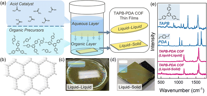
Here, we utilize the liquid–solid growth technique to explore morphology and crystallographic orientation, two critical thin film properties for future applications, of imine COF films grown directly onto substrates (Fig. 1a). We demonstrate that this residual/liquid–solid method produces films with consistent thicknesses on the nanometer level which could be used for future electronic and optical device fabrication. This is in contrast to films grown at the liquid–liquid interface which produces micron level variations in thickness and can suffer from poor adhesion to some substrates. Additionally, we also show that the acid concentration strongly affects the morphology of the liquid–solid TAPB-PDA COF films with those most smooth achieved when the molarity of the acid in the aqueous phase is kept within a certain range. Furthermore, we show that optimization of the growth time produces sub-20 nm films with nanometer level smoothness in just 30 minutes and illustrate that film orientation is strongly dependent upon growth conditions. These studies are culminated with a demonstration showing optimal films are semiconducting and function as the channel in organic electrochemical transistors.
Results and discussion
COF film growth via liquid–liquid and liquid–solid synthesis
COF thin films were synthesized using the condensation reaction of 1,3,5-tris(4-aminophenyl) benzene (TAPB) (13 mg, 0.04 mmol, 1.0 eq.) and p-phthalaldehyde (PDA) (7.5 mg, 0.06 mmol, 1.5 eq.), which were added to a 20 mL scintillation vial and dissolved in methylene chloride (8 mL) (Fig. 1a). Next, a Si/SiO2 substrate approximately 1 cm2 was placed at the bottom of the vial. Then 8 mL of aqueous acetic acid (from 1 M to 10 M) was slowly syringed on top of the organic layer ensuring minimal disruption of the solvent–solvent interface. TAPB-PDA COF (structure shown in Fig. 1b) film formation through liquid–liquid (LL) growth and liquid–solid (LS) growth began almost instantly upon adding the aqueous layer containing the catalyst (shown in Fig. 1c and d). After removing the substrate for LS growth, it was placed in a vial of acetone and briefly sonicated (<5 s) to remove large particulates from the surface. Chemical characterization of the TAPB-PDA COF grown both through the LL and LS methods was carried out using Raman spectroscopy. Fig. 1e reports the Raman spectra of the monomer powders (PDA and TAPB) as well as the TAPB-PDA COF from both growth methods. The Raman peaks associated with the starting monomers were not present in the final COF thin films. Expected C![[double bond, length as m-dash]](https://www.rsc.org/images/entities/char_e001.gif) N stretching modes at 1590 and 1560 cm−1 and aromatic stretching modes for C–H at 1160 cm−1 are instead present, indicating conversion of the monomer precursors to an imine network.35 Additionally, the Raman spectra of the LL and LS TAPB-PDA COF both showed the same spectra with the exception of the SiO2/Si substrate feature at 520 cm−1 in the case of the thinner films from LS growth. Scanning electron microscopy (SEM) and energy dispersive X-Ray spectroscopy (EDX) was used to distinguish the LS film from the substrate. Areas containing the film had a higher percentage of carbon, while areas with only substrate had a higher percentage of silicon (further information in Fig. S3 and S4†).
N stretching modes at 1590 and 1560 cm−1 and aromatic stretching modes for C–H at 1160 cm−1 are instead present, indicating conversion of the monomer precursors to an imine network.35 Additionally, the Raman spectra of the LL and LS TAPB-PDA COF both showed the same spectra with the exception of the SiO2/Si substrate feature at 520 cm−1 in the case of the thinner films from LS growth. Scanning electron microscopy (SEM) and energy dispersive X-Ray spectroscopy (EDX) was used to distinguish the LS film from the substrate. Areas containing the film had a higher percentage of carbon, while areas with only substrate had a higher percentage of silicon (further information in Fig. S3 and S4†).
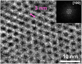
To fully characterize the TAPB-PDA COF (LS) and investigate the porosity, transmission electron microscopy (TEM) was conducted. An amorphous carbon coated TEM grid was attached to a silicon substrate and introduced to the LS growth setup. Afterwards, it was briefly sonicated to remove excess material and used for analysis. Fig. 2 shows a close-up real-space TEM image of the TAPB-PDA COF grown directly onto the TEM grid. The top right corner of Fig. 2 shows the corresponding fast Fourier transform (FFT) of the selected area indicating the periodicity originating from the [100] plane of the crystalline porous structure. It can clearly be noted that the pore size approaches 3.3 nm which closely matches previous literature reports of the same COF36 (see Fig. S5 and S6 in the ESI† for additional TEM images).
Acid concentration dependent film morphology with liquid–solid growth on substrate
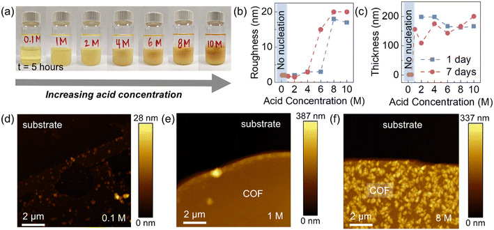
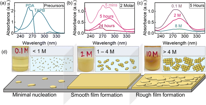
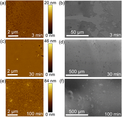
To study the effect of acid concentration on liquid–solid (LS) film growth, COF thin films were grown on Si/SiO2 wafers using a range of molarities of acetic acid (AcOH) in the aqueous layer. Shown in Fig. 3a, the higher concentrations of acetic acid showed the visible presence of particulates in the bottom organic layer after 5 hours, while the lowest acid concentration showed minimal color change and the absence of particulates in the organic solution (see additional Raman analysis in Fig. S7 and time-lapse photographs in Fig. S8 in the ESI†). To investigate the influence of acid molarity on film morphology, atomic force microscopy (AFM) was used to evaluate both surface roughness and film thickness (Fig. 3b and c). Roughness analysis of the films grown both over 1 day and 7 days at varying acetic acid molarities reveals that the acid concentration strongly affects the resultant surface roughness of the LS COF thin films (Fig. 3b). AFM shows that acetic acid molarities below 1 M result in very little nucleation or growth, as the catalyst concentration appears insufficiently high to initiate imine formation (Fig. 3d). AFM also shows that with acid concentrations between 1 and 4 M, complete film formation with nanoscale roughness less than 4 nm is achieved, indicating ideal conditions for smooth and continuous TAPB-PDA COF film synthesis in this study (Fig. 3e). Additional SEM analysis of this LS growth condition is also included in Fig. S9 in the ESI.† AFM shows that at higher acetic acid concentrations, the surface roughness dramatically increases as particulates ranging from 100–200 nm in area and approximately 15 nm in height form readily on the COF film (Fig. 3f). Film thicknesses for experiments range between 150–200 nm with minimal difference between 1 day and 7 day growth, presumably due to the formation of the interfacial film between liquid–liquid interfaces.The proposed thin film growth mechanism for acid-dependent growth of the TAPB-PDA COF (LS) is shown in Fig. 4d. For concentrations below 1 M, minimal film formation is observed, due to the limited concentration of COF oligomers present in solution and insufficient concentration of the acid to catalyze imine formation. However, when the acid concentration is between 1 M and 4 M, a generally smooth film is observed. This is due to the fact that sufficient acid has diffused across the liquid–liquid interface enabling a reaction between the monomers, and thus driving the coalescence of crystalline domains. As a result, it is proposed that adequate, yet small-sized COF oligomers are present in the solution throughout and can therefore deposit and react onto the substrate. This produces accelerated COF growth in the lateral direction while limiting variations in thickness to less than 2 nm. Chen et al. describes a similar phenomenon of organic film growth where through Ostwald ripening, adjacent thin islands merge as a result of their high surface-area-to-volume ratio and mobility on SiO2, leading to coalescence in the lateral direction. However, when the growing domain was isolated, it underwent a self-confined layer growth mode, leading to increase in the vertical direction.38 The film morphology was found to be related to the percentage of molecules contained in islands greater than the critical island size, and thus explains the observed film roughening shown in Fig. 3f. When the acid concentration is greater than 4 M, a rough film is formed presumably due to a large presence of the acid catalyst that has diffused across the liquid–liquid interface causing rapid uncontrolled imine bond formation between the monomers resulting large COF oligomers (Fig. 4d, right). These oligomers deposit onto the substrate surface and grow vertically to form a roughened film with large COF clusters throughout and thus restricts smooth film formation in the lateral direction. Similarly, an increase in film roughness has been observed in vapor–solid COF growth via chemical vapor deposition (CVD) at lower growth temperatures.39 In this case, film morphology and growth in the lateral versus vertical direction appear to be ultimately affected by the concentration of reacted monomers in solution.38,40
Orientation control
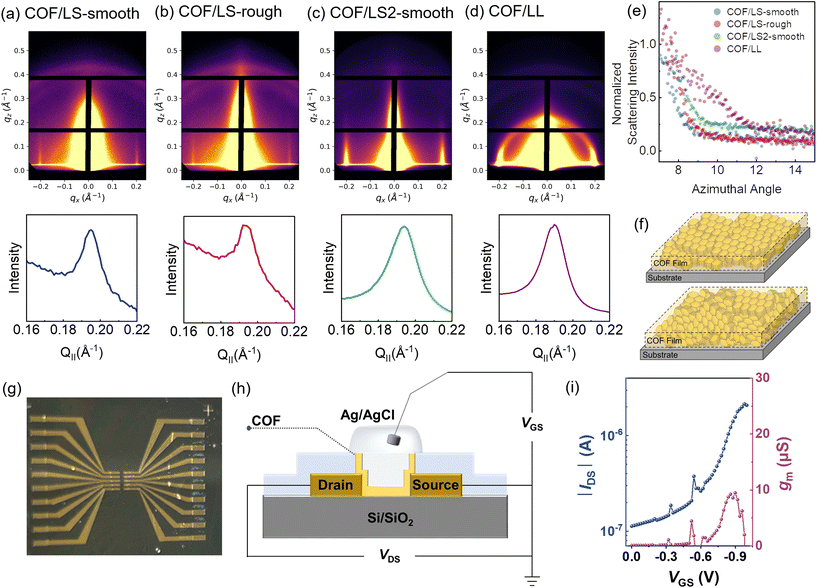
For future applications in electronic devices including sensors, ambipolar electronics, and transistors of different types, the control and manipulation of the COF film crystal orientation is critical. To study the influence of growth conditions on both the crystallinity and orientation of the TAPB-PDA COF thin films, grazing-incidence wide-angle X-ray scattering (GIWAXS) was performed. Prior to this analysis, the films underwent an annealing and subsequent activation step used to remove solvent and impurities from the pores43 (see further details on page S4 in the ESI†). The resulting scattering images and corresponding plots are shown in Fig. 6. Several different films were analyzed (Fig. 6a–d), including both liquid–solid (LS) growth and liquid–liquid (LL) growth, to understand the different effects of specific growth conditions. COF samples grown via LS growth on the substrate in both low and high acid concentrations exhibit a high degree of crystallinity with COF layers aligned parallel to the substrate surface (Fig. 6f, top). This level of crystallinity and orientation is retained even when the thickness of the COF film is increased after subjecting it to the same conditions again (Fig. 6c). More information on this regrowth experiment can be found in Fig. S16 and S17 in the ESI.† This preferred orientation is indicated by the vertical peaks that appear between 0.18 Å−1 and 0.21 Å−1 in Fig. 6a–c which correspond to the [100] of the hexagonal lattice.44–46 Using Bragg's law, the d-spacing for these planes was determined from the peak position, qmax, using the following equation:The d-spacings are 32.2 Å, 32.4 Å, 32.2 Å, and 33.2 Å for Fig. 6a–d, respectively which matches previous literature reports for the same COF.47,48 Additionally the PXRD data from the COF (LL) in Fig. S1† was converted to I vs. Q. The obtained pattern matches the 1D projection of the collected GIWAXS data from the COF (LS) (see Fig. S18 in the ESI†).
The parallel orientation of the COF relative to the surface of the substrate is a result of a few contributing factors of this unique interfacial growth setup. Firstly, the slow diffusion of the acetic acid across the liquid–liquid interface controls the precise deposition and therefore lateral growth of the COF with initial preferential parallel orientation. Also, the COF formed at the liquid–liquid interface between the aqueous and organic layers likely plays a role in continuing to slow and control the acid diffusion. This is evident for the LS growth based on the observed morphological features that occur when the acid concentration is changed as well as the early growth experiments depicted in the AFM images of Fig. 3 and 5, respectively. Secondly, the preference for parallel orientation is retained as the COF film continues to grow in the vertical direction. This is likely due to the favorable π–π interactions between the initial layers of COF and the layers that begin to form on top.49 This has been previously observed in works which describe the growth of COFs on single-layer graphene (SLG) and show that the thickness and uniformity of orientated films are also dependent on the underlying substrate.7,50 This is also evident in Fig. 6c, which shows that a COF film (LS) which was resubjected to the same growth conditions increases in thickness but retains parallel orientation.
Comparatively, the scattering image of the LL growth shown in Fig. 6d depicts a semicircle with bright spots at the edges and top, suggesting randomly oriented crystallites (Fig. 6f, bottom), similar to a powder.27 The azimuthal integration for each scattering image is shown below in Fig. 6. Fig. 6e shows the scattering intensity versus χ plots and distribution around the azimuth for COF samples in Fig. 6a–d. All LS growth samples (Fig. 6e; blue, pink, green) show a sharp decay in the azimuthal scattering from the [100] peak, indicating that the planes are vertically well-aligned with correlations in the direction parallel to the surface of the substrate. The LL film (purple) is the outlier in this graph with a distribution of mixed orientations of the [100] planes relative to the surface of the substrate. This is likely due to the dynamic nature of the liquid–liquid interface, which aids in COF crystallization but does not cause any preferential alignment. Previous work has shown that a polymer is required to guide the ordering and alignment of COF crystallization at a liquid–air interface.28
Semiconductor performance
Finally, we investigated TAPB-PDA COF films synthesized via the liquid–solid method as prospective semiconductor channels in organic electrochemical transistors (OECTs) (Fig. 6g). Organic electrochemical transistors operate by transducing a small gate voltage potential (VGS) into a channel current (IDS) between source and drain electrodes.51,52 The optical image of the OECTs array fabricated in this study is shown in Fig. 6h while device fabrication process is shown in the ESI (Fig. S19†). These OECTs have a channel dimension of 500 × 10 μm2 (width × length) and details can be found in the ESI.† The transfer curve (IDS–VGS) shown in Fig. 6i indicates a p-type (hole transport) operation. These devices show typical gate modulation of the channel current over a gate voltage range from 0 V to −0.95 V. The transconductance (gm), extracted from the slope of the transfer curve is a critical parameter for using an OECT as an amplifier. In this work, a maximum gm of approximately 9.5 μS at a gate voltage of −0.9 V is measured. Note, the low current/transconductance is expected considering the low semiconductor mass in the channel of these devices. Our TAPB-PDA COF films are quite thin (≈25 nm) and have very low density (0.38 g cm−3)53 compared to the typical conjugated organic polymers (≈100 nm thick, density > 1 g cm−3) commonly used in OECTs.54–56 Additionally, the hydrophobic nature of the COF channel57 may cause limited volumetric capacitance of electrochemical transistors operated in aqueous electrolyte. Future investigations of COF-based electrochemical transistors will focus on the optimization of COF film hydrophilicity,58 which can be affected by crystallinity and surface area, and enhancement of the semiconducting monomer components.Conclusions
Ensuring strict control of crystallographic orientation and morphology during COF thin film growth remains a crucial parameter for implementation of these exciting materials into electronic and photonic applications. In this study, an interfacial setup was used to synthesize COF thin films both at the liquid–liquid (LL) and liquid–solid (LS) interfaces at room temperature. The acetic acid concentration was found to strongly affect film morphology of the LS growth, where concentrations of 1–4 M enabled the formation of smooth films (<200 nm in thickness, 1–2 nm roughness) after 24 hours. Early growth experiments showed the evolution of LS film formation from patchy to smooth and uniform films and then to rougher and thicker films at longer growth times. GIWAXS studies highlight the difference in orientation between the LS growth and LL growth methods, where LS growth showed a high degree of parallel alignment to the surface of the substrate and LL growth showed mixed orientation. Finally, charge transport measurements of OECTs fabricated from the LS growth method demonstrate that the present COF films are a p-type semiconductor. In future applications utilizing transistors, optoelectronic devices, and catalytic films made from semiconducting COFs, understanding the pore alignment and crystal structure in COF thin films will be important as electronic properties are governed by a multitude of factors. Future work linking thin film synthesis to controllable electronic properties of COFs will be significant as these exciting materials continue to push the boundaries of wafer-scale organic electronic materials and potential device configurations.Author contributions
D. D. B., L. T., A. Re., Q. F., and C. M. performed COF synthesis and characterization. D. D. B., K. P., H. K. performed and evaluated GIWAXS experiments. A. Ru. performed SEM and surface characterization. C. H. performed TEM analysis. Y. Y. fabricated and evaluated OECT devices. D. D. B., T. J. M., A. F., L. D., L. B., Y. Z., J. L., J. K. and N. G. led the supervision of experiments and manuscript preparation and drafting.Conflicts of interest
There are no conflicts of interest.Acknowledgements
D. D. B., L. T., L. B., and N. G. acknowledge financial support from The Air Force Office of Scientific Research (AFOSR) grant number 23RXCOR011. A. F. and T. J. M. gratefully acknowledge financial support by AFOSR grant FA9550-22-1-0423. This material is based on research sponsored by AFRL under agreement number FA8650-22-2-5200. The U.S. Government is authorized to reproduce and distribute reprints for Governmental purposes notwithstanding any copyright notation thereon.References
- P. Côté, A. I. Benin, N. W. Ockwig, M. O'Keeffe, A. J. Matzger and O. M. Yaghi, Science, 2005, 310, 1166–1170 CrossRef PubMed.
- F. Haase and B. V. Lotsch, Chem. Soc. Rev., 2020, 49, 8469–8500 RSC.
- S. Kandambeth, K. Dey and R. Banerjee, J. Am. Chem. Soc., 2019, 141, 1807–1822 CrossRef CAS PubMed.
- L. K. Beagle, Q. Fang, L. D. Tran, L. A. Baldwin, C. Muratore, J. Lou and N. R. Glavin, Mater. Today, 2021, 51, 427–448 CrossRef CAS.
- J. L. Fenton, D. W. Burke, D. Qian, M. Olvera de la Cruz and W. R. Dichtel, J. Am. Chem. Soc., 2021, 143, 1466–1473 CrossRef CAS PubMed.
- E. L. Spitler, B. T. Koo, J. L. Novotney, J. W. Colson, F. J. Uribe-Romo, G. D. Gutierrez, P. Clancy and W. R. Dichtel, J. Am. Chem. Soc., 2011, 133, 19416–19421 CrossRef CAS PubMed.
- J. W. Colson, A. R. Woll, A. Mukherjee, M. P. Levendorf, E. L. Spitler, V. B. Shields, M. G. Spencer, J. Park and W. R. Dichtel, Science, 2011, 332, 228–231 CrossRef CAS PubMed.
- E. L. Spitler, J. W. Colson, F. J. Uribe-Romo, A. R. Woll, M. R. Giovino, A. Saldivar and W. R. Dichtel, Angew. Chem., Int. Ed., 2012, 51, 2623–2627 CrossRef CAS PubMed.
- D. D. Medina, V. Werner, F. Auras, R. Tautz, M. Dogru, J. Schuster, S. Linke, M. Döblinger, J. Feldmann, P. Knochel and T. Bein, ACS Nano, 2014, 8, 4042–4052 CrossRef CAS PubMed.
- R. DeBlase, K. Hernández-Burgos, K. E. Silberstein, G. G. Rodríguez-Calero, R. P. Bisbey, H. D. Abruña and W. R. Dichtel, ACS Nano, 2015, 9, 3178–3183 CrossRef PubMed.
- X. Gou, Q. Zhang, Y. Wu, Y. Zhao, X. Shi, X. Fan, L. Huang and G. Lu, RSC Adv., 2016, 6, 39198–39203 RSC.
- D. Medina, M. L. Petrus, A. N. Jumabekov, J. T. Margraf, S. Weinberger, J. M. Rotter, T. Clark and T. Bein, ACS Nano, 2017, 11, 2706–2713 CrossRef CAS PubMed.
- L. D. Tran, B. J. Ree, A. Ruditskiy, L. K. Beagle, R. C. Selhorst, D. D. Bhagwandin, P. Miesle, L. F. Drummy, M. F. Durstock, R. Rao, H. Koerner, N. R. Glavin and L. A. Baldwin, Adv. Mater. Interfaces, 2023, 10, 2300042 CrossRef CAS.
- L. Ascherl, E. W. Evans, M. Hennemann, D. Di Nuzzo, A. G. Hufnagel, M. Beetz, R. H. Friend, T. Clark, T. Bein and F. Auras, Nat. Commun., 2018, 9, 3802 CrossRef PubMed.
- T. Sick, A. G. Hufnagel, J. Kampmann, I. Kondofersky, M. Calik, J. M. Rotter, A. Evans, M. Döblinger, S. Herbert, K. Peters, D. Böhm, P. Knochel, D. D. Medina, D. Fattakhova-Rohlfing and T. Bein, J. Am. Chem. Soc., 2018, 140, 2085–2092 CrossRef CAS PubMed.
- M. Evans, A. Giri, V. K. Sangwan, S. Xun, M. Bartnof, C. G. Torres-Castanedo, H. B. Balch, M. S. Rahn, N. P. Bradshaw, E. Vitaku, D. W. Burke, H. Li, M. J. Bedzyk, F. Wang, J.-L. Brédas, J. A. Malen, A. J. H. McGaughey, M. C. Hersam, W. R. Dichtel and P. E. Hopkins, Nat. Mater., 2021, 20, 1142–1148 CrossRef PubMed.
- S. Cai, B. Sun, X. Li, Y. Yan, A. Navarro, A. Garzón-Ruiz, H. Mao, R. Chatterjee, J. Yano, C. Zhu, J. A. Reimer, S. Zheng, J. Fan, W. Zhang and Y. Liu, ACS Appl. Mater. Interfaces, 2020, 12, 19054–19061 CrossRef CAS PubMed.
- Y. Chen, H. Cui, J. Zhang, K. Zhao, D. Ding, J. Guo, L. Li, Z. Tian and Z. Tang, RSC Adv., 2015, 5, 92573–92576 RSC.
- S. Lin, C. S. Diercks, Y.-B. Zhang, N. Kornienko, E. M. Nichols, Y. Zhao, A. R. Paris, D. Kim, P. Yang, O. M. Yaghi and C. J. Chang, Science, 2015, 349, 1208–1213 CrossRef CAS PubMed.
- L. Ascherl, E. W. Evans, J. Gorman, S. Orsborne, D. Bessinger, T. Bein, R. H. Friend and F. Auras, J. Am. Chem. Soc., 2019, 141, 15693–15699 CrossRef CAS PubMed.
- S. Jhulki, A. M. Evans, X.-L. Hao, M. W. Cooper, C. H. Feriante, J. Leisen, H. Li, D. Lam, M. C. Hersam, S. Barlow, J.-L. Brédas, W. R. Dichtel and S. R. Marder, J. Am. Chem. Soc., 2020, 142, 783–791 CrossRef CAS PubMed.
- S. Zhang, Q. Yang, X. Xu, X. Liu, Q. Li, J. Guo, N. L. Torad, S. M. Alshehri, T. Ahamad, M. S. A. Hossain, Y. V. Kaneti and Y. Yamauchi, Nanoscale, 2020, 12, 15611–15619 RSC.
- S. Zhang, W. Xia, Q. Yang, Y. Valentino Kaneti, X. Xu, S. M. Alshehri, T. Ahamad, Md. S. A. Hossain, J. Na, J. Tang and Y. Yamauchi, Chem. Eng. J., 2020, 396, 125154 CrossRef CAS.
- D. Medina, J. M. Rotter, Y. Hu, M. Dogru, V. Werner, F. Auras, J. T. Markiewicz, P. Knochel and T. Bein, J. Am. Chem. Soc., 2015, 137, 1016–1019 CrossRef CAS PubMed.
- R. P. Bisbey, C. R. DeBlase, B. J. Smith and W. R. Dichtel, J. Am. Chem. Soc., 2016, 138, 11433–11436 CrossRef CAS PubMed.
- Y. Yang, C. Schäfer and K. Börjesson, Chem, 2022, 8, 2217–2227 CAS.
- D. D. Bhagwandin, J. H. Dunlap, L. D. Tran, A. Reidell, D. Austin, A. A. Putnam-Neeb, M. Loveday, R. Rao, L. A. Baldwin and N. R. Glavin, CrystEngComm, 2024, 26, 27–31 RSC.
- Z. Ou, B. Liang, Z. Liang, F. Tan, X. Dong, L. Gong, P. Zhao, H. Wang, Y. Zou, Y. Xia, X. Chen, W. Liu, H. Qi, U. Kaiser and Z. Zheng, J. Am. Chem. Soc., 2022, 144, 3233–3241 CrossRef CAS PubMed.
- S. Kim and H. C. Choi, ACS Omega, 2020, 5, 948–958 CrossRef CAS PubMed.
- Q.-W. Meng, S. Wu, M. Liu, Q. Guo, W. Xian, X. Zuo, S. Wang, H. Yin, S. Ma and Q. Sun, Sci. Adv., 2023, 9, eadh0207 CrossRef CAS PubMed.
- T. Zhang, X. Fu, C. Wu, F. J. Tan, Y. Liu and S. Xia, J. Environ. Chem. Eng., 2021, 9, 106807 CrossRef CAS.
- M. Matsumoto, L. Valentino, G. M. Stiehl, H. B. Balch, A. R. Corcos, F. Wang, D. C. Ralph, B. J. Mariñas and W. R. Dichtel, Chem, 2018, 4, 308–317 CAS.
- K. Dey, M. Pal, K. C. Rout, S. H. Kunjattu, A. Das, R. Mukherjee, U. K. Kharul and R. Banerjee, J. Am. Chem. Soc., 2017, 139, 13083–13091 CrossRef CAS PubMed.
- K Mahato, S. Bag, H. S. Sasmal, K. Dey, I. Giri, M. Linares-Moreau, C. Carbonell, P. Falcaro, E. B. Gowd, R. K. Vijayaraghavan and R. Banerjee, J. Am. Chem. Soc., 2021, 143, 20916–20926 CrossRef PubMed.
- S. A. Ahmed, Q. Liao, Q. Shen, M. M. F. Ashraf Baig, J. Zhou, C. Shi, P. Muhammad, S. Hanif, K. Xi, X. Xia and K. Wang, Chem. – Eur. J., 2020, 26, 12996–13001 CrossRef CAS PubMed.
- D. Zhu, J.-J. Zhang, X. Wu, Q. Yan, F. Liu, Y. Zhu, X. Gao, M. M. Rahman, B. I. Yakobson, P. M. Ajayan and R. Verduzco, Chem. Sci., 2022, 13, 9655–9667 RSC.
- R. L. Li, N. C. Flanders, A. M. Evans, W. Ji, I. Castano, L. X. Chen, N. C. Gianneschi and W. R. Dichtel, Chem. Sci., 2019, 10, 3796–3801 RSC.
- H. Chen, M. Li, Z. Lu, X. Wang, J. Yang, Z. Wang, F. Zhang, C. Gu, W. Zhang, Y. Sun, J. Sun, W. Zhu and X. Guo, Nat. Commun., 2019, 10, 3872 CrossRef PubMed.
- J. P. Daum, A. Ajnsztajn, S. A. Iyengar, J. Lowenstein, S. Roy, G. Gao, E. H. R. Tsai, P. M. Ajayan and R. Verduzco, ACS Nano, 2023, 17, 21411–21419 CrossRef PubMed.
- D. Cui, Y. Fang, O. MacLean, D. F. Perepichka, F. Rosei and S. Clair, Chem. Commun., 2019, 55, 13586–13589 RSC.
- H. S. Sasmal, A. Halder, S. H. Kunjattu, K. Dey, A. Nadol, T. G. Ajithkumar, P. R. Bedadur and R. Banerjee, J. Am. Chem. Soc., 2019, 141, 20371–20379 CrossRef CAS PubMed.
- D. D. Medina, V. Werner, F. Auras, R. Tautz, M. Dogru, J. Schuster, S. Linke, M. Döblinger, J. Feldmann, P. Knochel and T. Bein, ACS Nano, 2014, 8, 4042–4052 CrossRef CAS PubMed.
- D. Zhu and R. Verduzco, ACS Appl. Mater. Interfaces, 2020, 12, 33121–33127 CrossRef CAS PubMed.
- J. W. Colson, A. R. Woll, A. Mukherjee, M. P. Levendorf, E. L. Spitler, V. B. Shields, M. G. Spencer, J. Park and W. R. Dichtel, Science, 2011, 332, 228–231 CrossRef CAS PubMed.
- S.-L. Cai, Y.-B. Zhang, A. B. Pun, B. He, J. Yang, F. M. Toma, I. D. Sharp, O. M. Yaghi, J. Fan, S.-R. Zheng, W.-G. Zhang and Y. Liu, Chem. Sci., 2014, 5, 4693–4700 RSC.
- M. Evans, A. Giri, V. K. Sangwan, S. Xun, M. Bartnof, C. G. Torres-Castanedo, H. B. Balch, M. S. Rahn, N. P. Bradshaw, E. Vitaku, D. W. Burke, H. Li, M. J. Bedzyk, F. Wang, J.-L. Brédas, J. A. Malen, A. J. H. McGaughey, M. C. Hersam, W. R. Dichtel and P. E. Hopkins, Nat. Mater., 2021, 20, 1142–1148 CrossRef PubMed.
- J. Smith, A. C. Overholts, N. Hwang and W. R. Dichtel, Chem. Commun., 2016, 52, 3690–3693 RSC.
- R. L. Li, A. Yang, N. C. Flanders, M. T. Yueng, D. T. Sheppard and W. R. Dichtel, Two Dimensional Covalent Organic Framework Solid Solutions, J. Am. Chem. Soc., 2021, 143, 7081–7087 CrossRef CAS PubMed.
- H. Wang, B. He, F. Liu, C. Stevens, M. A. Brady, S. Cai, C. Wang, T. P. Russell, T.-W. Tan and Y. Liu, J. Mater. Chem. C, 2017, 5, 5090–5095 RSC.
- B. Sun, C.-H. Zhu, Y. Liu, C. Wang, L.-J. Wan and D. Wang, Chem. Mater., 2017, 29, 4367–4374 CrossRef CAS.
- W. Huang, J. Chen, Y. Yao, D. Zheng, X. Ji, L.-W. Feng, D. Moore, N. R. Glavin, M. Xie, Y. Chen, R. M. Pankow, A. Surendran, Z. Wang, Y. Xia, L. Bai, J. Rivnay, J. Ping, X. Guo, Y. Cheng, T. J. Marks and A. Facchetti, Nature, 2023, 613, 496–502 CrossRef CAS PubMed.
- Y. Yao, W. Huang, J. Chen, X. Liu, L. Bai, W. Chen, Y. Cheng, J. Ping, T. J. Marks and A. Facchetti, Adv. Mater., 2023, 35, 2209906 CrossRef CAS PubMed.
- Q. Fang, Z. Pang, Q. Ai, Y. Liu, T. Zhai, D. Steinbach, G. Gao, Y. Zhu, T. Li and J. Lou, Proc. Natl. Acad. Sci. U. S. A., 2023, 120, e2208676120 CrossRef CAS PubMed.
- P. R. Paudel, J. Tropp, V. Kaphle, J. D. Azoulay and B. Lüssem, J. Mater. Chem. C, 2021, 9, 9761–9790 RSC.
- M. Yamashita, C. Otani, H. Okuzaki and M. Shimizu, in 2011 XXXth URSI General Assembly and Scientific Symposium, IEEE, Istanbul, 2011, pp. 1–4.
- C. M. Proctor, J. Rivnay and G. G. Malliaras, J. Polym. Sci., Part B: Polym. Phys., 2016, 54, 1433–1436 CrossRef CAS.
- D. Mullangi, S. Shalini, S. Nandi, B. Choksi and R. Vaidhyanathan, J. Mater. Chem. A, 2017, 5, 8376–8384 RSC.
- L. D. Tran, K. F. Presley, J. K. Streit, J. Carpena-Núñez, L. K. Beagle, T. A. Grusenmeyer, M. J. Dalton, R. A. Vaia, L. F. Drummy, N. R. Glavin and L. A. Baldwin, Chem. Mater., 2022, 34, 529–536 CrossRef CAS.
Footnote |
| † Electronic supplementary information (ESI) available. See DOI: https://doi.org/10.1039/d3nr05798d |
| This journal is © The Royal Society of Chemistry 2024 |


