
Biomass-derived lightweight SiC aerogels for superior thermal insulation†
Chunxue
Zheng
ab,
Xinyang
Li
 *ab,
Jie
Yu
*a,
Zhulin
Huang
ab,
Ming
Li
ab,
Xiaoye
Hu
*ab and
Yue
Li
ac
*ab,
Jie
Yu
*a,
Zhulin
Huang
ab,
Ming
Li
ab,
Xiaoye
Hu
*ab and
Yue
Li
ac
aKey Laboratory of Materials Physics and Anhui Key Laboratory of Nanomaterials and Nanotechnology, Institute of Solid State Physics, HFIPS, Chinese Academy of Sciences, Hefei, 230031, P. R. China
bUniversity of Science and Technology of China, Hefei 230026, P. R. China. E-mail: hxy821982@issp.ac.cn
cTiangong University, Tianjin, 300387, China
First published on 24th January 2024
Abstract
Silicon carbide (SiC) aerogels, which possess unique porous structure and high ablation resistance, show great potential as thermal insulation materials, but their wide application is limited by expensive and cumbersome synthetic procedures. Therefore, it is pivotal to develop a facile, versatile, and cost-effective method for producing SiC aerogels. Herein, we have successfully prepared ultra-light SiC nanowire aerogels (SNWAs) boasting remarkably low thermal conductivity, using biomass-derived carbon templates (BCTs) through a direct carbothermal reduction method. The BCTs obtained by simply carbonizing freeze-dried eggplants can serve not only as the carbon sources but also as the templates for the in situ growth of SiC nanowires. The resultant three-dimensional (3D) SNWAs possess various porous structures, incorporating the original micro-sized pores inherited from the eggplant and nano-sized pores constructed from interconnected SiC nanowires. These multi-scale pore structures bestow SNWAs with lower gas-phase heat conduction characteristics. Besides, the numerous stacking faults and heterojunctions present in the SiC nanowires play a key role in obstructing the solid-phase heat transfer and reinforcing the SiC skeleton. As a result, the SNWAs show an exceptionally low thermal conductivity, measuring 0.0149 W m−1 K−1 at room temperature, and maintain this low value (0.0256 W m−1 K−1) even at 500 °C. Remarkably, even after being exposed to air at 1200 °C for 2 h, the SNWAs maintain a low thermal conductivity of 0.0226 W m−1 K−1. Such low-cost and effective preparation of biomass-derived SiC aerogels is anticipated to pave a new avenue for the development of advanced thermal insulators.
 Xinyang Li | Xinyang Li is currently an associate researcher at the Institute of Solid State Physics, Hefei Institute of Physical Science, Chinese Academy of Sciences. She graduated from Wuhan University of Science and Technology in 2013. After that, she worked as an assistant researcher at the Institute of Solid State Physics. Her research interests are in the fields of the design and synthesis of thermal protection and thermal insulation materials under high temperature, such as ultra-high temperature ceramics, ceramic fibers and ceramic aerogels. |
1. Introduction
Thermal insulation materials based on ceramics hold tremendous promise in the fields of energy conservation and thermal protection.1 Amidst the development of ceramics-based thermal insulation, ceramic aerogels,1–3 distinguished by their three-dimensional porous network structures, have recently gained significant attention due to their remarkable attributes, such as low thermal conductivity and exceptional stability. Nonetheless, several intrinsic limitations of conventional oxide ceramic nanoparticles, such as SiO2 and Al2O3, hinder the widespread use of ceramic aerogels.4–6 In particular, the structure of nanoparticles connected by narrow interparticle necks inherently leads to the brittle nature of nanoparticle-based ceramic aerogels.7,8 In addition, oxide ceramic nanoparticles have a tendency to undergo grain growth and phase transformation in high-temperature environments, thus resulting in catastrophic failure of ceramic aerogels.9–11 Consequently, there is a compelling need to explore advanced ceramic aerogels with high stability and low thermal conductivity for thermal insulation applications under high temperatures.Within this context, silicon carbide (SiC), distinguished by its favorable high-temperature stability and superior sintering resistance compared to conventional oxide ceramics, has exhibited significant potential in the realm of thermal insulation, especially under extreme conditions.12 This has led to a surge in the exploration of SiC aerogels, particularly those constructed from SiC nanowires with elastically interconnected three-dimensional structures.13–15 For instance, Su et al. prepared a highly porous three-dimensional SiC NWA constructed from a multitude of interwoven 3C-SiC nanowires, which is promising for thermal insulator applications under extreme conditions.16 Additionally, Song et al. have demonstrated the exceptional thermal insulation properties of SiC@SiO2 nanofiber aerogels, prepared through a straightforward chemical vapor deposition method followed by heat treatment.17 However, despite the substantial potential of SiC nanowire aerogels, their preparation methods predominantly rely on costly and intricate synthetic processes, thereby constraining their practical application. Clearly, considerable challenges remain to fabricate SiC nanowire aerogels with high thermal stability and low thermal conductivity by economical and efficient methods.
In this work, we develop a facile, universal and low-cost method for the preparation of 3D SNWAs by employing low-cost, biomass-derived carbon as both templates and carbon sources, followed by the in situ growth of SiC nanowires. By leveraging the multi-scale porous structures within the 3D network and the abundance of stacking faults and heterojunctions within each SiC nanowire, the SNWAs demonstrate exceptional thermal insulation properties. These SNWAs exhibit an impressively low thermal conductivity, measuring just 0.0149 W m−1 K−1, and maintain a remarkably low thermal conductivity of 0.0226 W m−1 K−1 even after being exposed to high-temperature oxidation in air. Furthermore, it is noteworthy that various other biomass materials, such as Pleurotus eryngii fungus and gourds, can also be transformed into SiC nanowire aerogels using this method. This indicates the universality of this approach for converting biomass materials into high-temperature-resistant ceramic aerogels.
2. Experimental
2.1. Materials preparation
The eggplant (Solanum melongena L.), Pleurotus eryngii fungus and gourd were purchased locally. Ethanol (EtOH, ≥99.7%) and HCl (36.0–38.0%) were purchased from Sinopharm Chemical Reagent Co., Ltd. Tetraethyl orthosilicate (TEOS, 98%), and tert-butanol (TBA, ≥99.5%) were obtained from Aladdin. Deionized (DI) water was prepared with a Milli-Q water purification system. All chemicals were used without any purification.2.2. Preparation of biomass-derived carbon templates
The peeled eggplants were first cut into the desired shape and then immersed in the TBA solvent, followed by a freeze-drying process to create dried eggplant pieces. These dried eggplant pieces were carbonized at 800 °C for 2 h under an Ar atmosphere to obtain the biomass-derived carbon templates (BCTs). The same treatment was applied to other biomass materials, such as Pleurotus eryngii fungus and gourds, to obtain the corresponding BCTs.2.3. Synthesis of SiC nanowire aerogels
Typically, the sol utilized for impregnating the BCTs was first prepared and the corresponding preparation procedure is shown in Fig. 1. Specifically, TEOS was first added into the mixture of EtOH and DIW (1![[thin space (1/6-em)]](https://www.rsc.org/images/entities/char_2009.gif) :1 by volume) to produce 20 mL of the sol, followed by the addition of HCl as pH modifier to adjust the pH value to ca. 3. Then, the BCTs (120 mg) were immersed in 20 mL of the sol, and vacuum degassed for 3 h to ensure that the pores in BCTs were thoroughly filled. These samples were subsequently dried in an oven at 60 °C for 12 h and then annealed in a tube furnace to obtain SiC nanowire aerogels (SNWAs). The annealing temperature was gradually increased to 800 °C at a rate of 2 °C min−1 to maintain the original structure of the BCTs. Subsequently, the temperature was further raised to 1500 °C at a rate of 5 °C min−1 and the BCTs kept for 3 h under the Ar atmosphere. After naturally cooling down to room temperature, the SNWAs were obtained. The SNWAs were prepared with different concentrations of TEOS (0.1, 0.125, 0.167, 0.25 and 0.5 M) and denoted as SNWAs-1, SNWAs-2, SNWAs-3, SNWAs-4 and SNWA-5, respectively.
:1 by volume) to produce 20 mL of the sol, followed by the addition of HCl as pH modifier to adjust the pH value to ca. 3. Then, the BCTs (120 mg) were immersed in 20 mL of the sol, and vacuum degassed for 3 h to ensure that the pores in BCTs were thoroughly filled. These samples were subsequently dried in an oven at 60 °C for 12 h and then annealed in a tube furnace to obtain SiC nanowire aerogels (SNWAs). The annealing temperature was gradually increased to 800 °C at a rate of 2 °C min−1 to maintain the original structure of the BCTs. Subsequently, the temperature was further raised to 1500 °C at a rate of 5 °C min−1 and the BCTs kept for 3 h under the Ar atmosphere. After naturally cooling down to room temperature, the SNWAs were obtained. The SNWAs were prepared with different concentrations of TEOS (0.1, 0.125, 0.167, 0.25 and 0.5 M) and denoted as SNWAs-1, SNWAs-2, SNWAs-3, SNWAs-4 and SNWA-5, respectively.
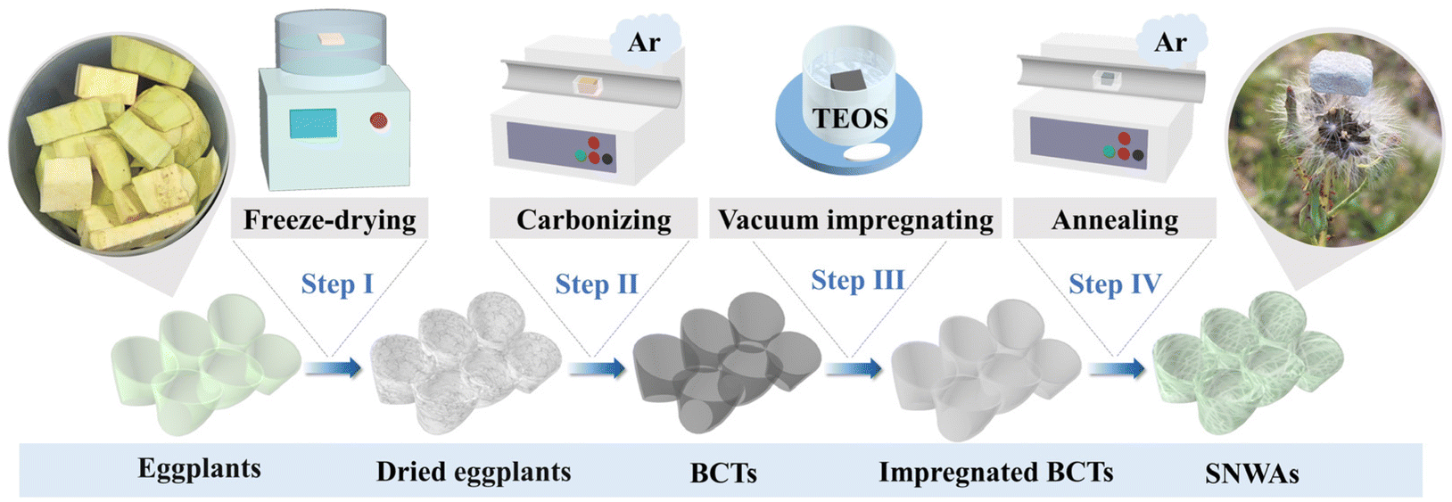 | ||
| Fig. 1 Schematic illustration of the preparation procedure of the 3D SNWAs. | ||
2.4. Characterization
The structure and morphology of the prepared SNWAs were investigated using field-emission scanning electron microscopy (SEM, Hitachi, SU8020, Japan) and transmission electron microscopy (TEM, Tecnai G2 F20, USA) equipped with an Oxford Instruments IE250X-Max50 energy dispersive spectrometer (EDS). High-angle annular dark field (HAADF) images and corresponding elemental mapping images were also acquired on the Tecnai G2 F20 instrument. X-ray diffraction (XRD) patterns of SNWAs were obtained on an X′ Pert Philips diffractometer with Cu Kα radiation (0.154056 nm). X-ray photoelectron spectroscopy (XPS) characterization was performed on a Thermo Scientific K-Alpha instrument (Thermo ESCALAB 250XI) using a monochromatized Al Kα X-ray source (1486.6 eV). Fourier transform infrared (FTIR) spectra of the prepared samples were recorded on an infrared spectrometer (Nicolet 8700). Raman spectra were acquired using a Renishaw inVia Raman microscopy spectrometer with a 532 nm laser. The accumulation time was 1 s in a single acquisition. The effective laser output was ca. 10 mW. N2 adsorption–desorption isotherms were obtained on Quantachrome ASiQ. The pore size distribution plots were recorded from the adsorption branch of the isotherm based on the Barrett–Joyner–Halenda (BJH) and non-local density functional theory (DFT) models.2.5. Thermal conductivity test
The thermal stability of the samples was analyzed by thermogravimetric analysis (TGA/DSC + 3, Mettler Toledo, Switzerland) in an air atmosphere, covering a temperature range from 25 to 1200 °C. Visualization of the heat transfer process in the aerogel was achieved using infrared thermography (Fluke Ti200, USA). During the test, the samples were placed on a heating platform and the temperature of the upper surface of the sample was recorded by photographing it with an infrared thermographic camera at regular intervals. The thermal diffusivity was measured using a laser flash technique (LFA457, Germany). The density of the samples was determined by measuring their mass and volume using an electronic analytical balance and a micrometer, respectively. The thermal conductivity (K) of the samples can be calculated using the following formula:| K = α·CP·ρ |
3. Results and discussion
3.1 Characterization of the SNWAs
Eggplants were selected as raw materials to prepare the biomass-derived carbon templates (BCTs) because they are rich in carbon and oxygen elements, which make them ideal templates for the in situ growth of SiC. As shown in Fig. 1, the freeze-dried eggplants were simply carbonized to obtain BCTs. After the carbonization process, the BCTs underwent a volume shrinkage of approximately 30% compared to the freeze-dried eggplants (Fig. S1†). This reduction in size is due to the dehydration and carbonization during the heat treatment. However, it is reassuring to note that the original structure and internal porous structure of the eggplants were well maintained in the BCTs and the SNWAs-3 (Fig. 3a and S4†). Besides, as shown in Fig. S2,† large amounts of carbon and oxygen elements were evenly distributed in the BCTs, which can be beneficial for the in situ growth of SiC nanowires on them. The BCTs were then vacuum-impregnated in the siloxane sol prepared with TEOS as the silicon source,18,19 followed by atmospheric drying at 60 °C, to form siloxane xerogel-loaded BCTs. The SNWAs were subsequently prepared by a simple annealing of the siloxane xerogel-loaded BCTs at 1500 °C in an Ar atmosphere for 3 h. During this process, the BCTs can serve not only as the templates for the growth of SiC nanowires, but also as the carbon precursors to react with Si-containing precursors via carbothermal reduction, to obtain SNWAs. The growth mechanism of the SiC NWs from siloxane xerogel-loaded BCTs can be described as follows (where g, l, or s indicate the physical state of gas, liquid or solid, respectively):| Si(OC2H5)4(g) → SiO2(s) + 2H2O(g) + 4C2H4(g) | (1) |
| SiO2(s, l) + C(s) → SiO(g) + CO(g) | (2) |
| SiO2(s, l) + 2C(s) → SiC(s) + CO2(g) | (3) |
| SiO(g) + 3CO(g) → SiC(s) + 2CO2(g) | (4) |
As shown in Fig. 2, with the rise in temperature, the decomposition of siloxane xerogel could be initiated, where the siloxane xerogel was vaporized at ca. 160 °C to generate activated SiO2 (reaction (1)).20 The activated SiO2 was then reduced by the solid phase carbon (provided by the BCTs) to produce gaseous SiO and CO (reaction (2)).20 Afterward, there are two types of reactions that lead to the formation of SiC. One is the solid/liquid–solid reaction between SiO2 and the carbon template, which ultimately generates SiC on the surface of the BCTs (reaction (3)). The original structure of the BCTs can be well-maintained through this reaction.The other is the vapour–vapour reaction between the gaseous SiO and CO, which gives rise to the continuous growth of SiC nanowires (reaction (4)).21 All of these reactions create a cycle that continuously generates a large number of interconnected SiC nanowires and eventually leads to the formation of the three-dimensional (3D) SNWAs. As shown in Fig. S1,† the optical photograph reveals that the SNWAs appear light green, which is the natural color of the SiC nanowires. Notably, the density of the SNWAs prepared in this work ranges from 36 to 65 mg cm−3 with the increasing TEOS concentration (Table S1†), and it is so light that a dandelion can easily support a piece of SNWAs with a size of 15 × 15 × 5 mm3 (Fig. 1).
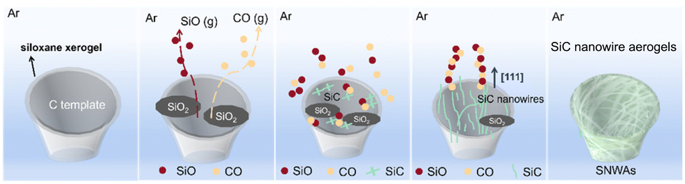 | ||
| Fig. 2 Schematic illustration of the growth mechanism of the SiC nanowires derived from the BCTs. | ||
The morphology and microstructure of the SNWAs were investigated via scanning electron microscopy (SEM) and transmission electron microscopy (TEM) characterization methods. Specifically, SiC nanowire-based aerogels with varying concentration of TEOS, including 0.1 M (SNWAs-1), 0.125 M (SNWAs-2), 0.167 M (SNWAs-3), 0.25 M (SNWAs-4) and 0.5 M (SNWAs-5), are investigated (Fig. 3). Typically, all the samples show similar porous 3D network structures, where their scaffolds are constructed from the abundant inter-crosslinked SiC nanowires. It should be noted that at relatively low Si source concentrations, SNWAs-1 and SNWAs-2 exhibit not only many interconnected nanowires but also apparent templates of remaining BCTs, suggesting the incomplete transformation of the BCTs at low concentrations of the Si source. Upon increasing the TEOS concentration to 0.167 M, uniformly distributed and inter-crosslinked SiC nanowires can be observed, implying the complete transformation of siloxane xerogel-loaded BCTs into SNWAs. However, upon further increasing the TEOS concentration (SNWAs-4 and SNWAs-5), amorphous silicon oxide (SiO2) phases appear at junctions of the crosslinked SiC nanowire network, which can be adverse to subsequent thermal protection applications. Based on the SEM characterization, it can be confirmed that the TEOS concentration of 0.167 M is the optimal condition for the preparation of the SNWAs. Then, we studied further the structure of the optimized SNWAs-3 via TEM (Fig. 4a) and HRTEM (Fig. 4b) characterization methods. In detail, the smooth surface of the SiC nanowires with the β-SiC structure can be found. In addition, the d-spacing of electron diffraction (SAED) patterns of SNWAs-3 further proves its single-crystal structure (Fig. 4c). Notably, a lot of junctions with the stacking faults can be found between SiC nanowires (Fig. 4d–h). These junctions can be beneficial for reducing the solid phase thermal conductivity of the SNWAs through scattering phonons of different frequencies.22
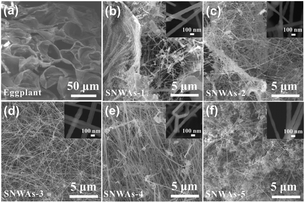 | ||
| Fig. 3 SEM images and the zoomed-in images (inset) of (a) BCTs, (b) SNWAs-1, (c) SNWAs-2, (d) SNWAs-3, (e) SNWAs-4 and (f) SNWAs-5. | ||
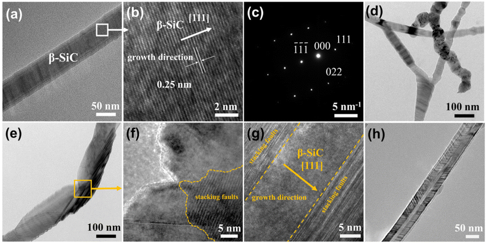 | ||
| Fig. 4 TEM (a) and HRTEM (b) images of SNWAs-3. (c) SAED pattern of the SNWAs-3. (d) TEM image of the junctions of SiC nanowires in SNWAs. (e–g) TEM images of stacking faults inside the nanowire. (h) Equivalent surface growth of a nanowire extension. | ||
The effects of the Si source concentration on the composition of the samples were further investigated by XRD. As shown in Fig. 5a, the strong diffraction peaks of the β-SiC crystal structure can be detected in all samples. The peaks located at 35.7°, 41.4°, 60.0°, 71.9° and 75.5° are, respectively, attributed to the (1 1 1), (2 0 0), (2 2 0), (3 1 1) and (2 2 2) planes of the β-SiC structure (JCPDS Card No. 29-1129).23 For the SNWAs-1 and SNWAs-2, their patterns show a broad diffraction peak located at 22.3°, which corresponds to amorphous carbon.24 This result further corroborates the incomplete transformation of the BCTs due to the insufficient concentration of the Si source. With the increasing concentration of the Si source, the peak at 22.3° disappears, manifesting the complete transformation of BCTs. In addition, the peak at 33.6° attributed to be the stacking fault of the (1 1 1) plane,25 becomes apparent. This indicates the emergence of the stacking defects on the SNWAs-3. In addition, no obvious XRD peaks attributed to impurities can be observed, implying its high purity. As the concentration of the silicon source further increases (i.e., SNWAs-3 and SNWAs-4), the broad and weak peaks located between 20° and 30° assigned to the amorphous SiO2 (JCPDS Card No. 47-715)26 can be detected, suggesting the transformation of excess Si sources into amorphous SiO2, which can suppress the thermal insulation properties of the prepared samples.
 | ||
| Fig. 5 (a) XRD patterns and (b) XPS survey spectra of SNWAs-1, SNWAs-2, SNWAs-3, SNWAs-4 and SNWAs-5. High-resolution C 1s (c), Si 2p (d) and O 1s (e) XPS spectra of SNWAs-1, SNWAs-2, SNWAs-3, SNWAs-4 and SNWAs-5. (f) FTIR and (g) Raman spectra of the SNWAs-3. (h) Nitrogen adsorption–desorption isotherms and the specific surface area (SBET) of different prepared samples. (i) DFT and (j) BJH pore size distributions of SNWAs-3. | ||
To further confirm the high purity of the SNWAs-3, we performed X-ray photoelectron spectroscopy (XPS) characterization to investigate its valence state and chemical composition. XPS survey spectra of SNWAs (Fig. 5b) reveal that SNWAs-3 is composed of C, Si, and O elements, where the absorption peaks located at 532.1, 283.1, 152.1 and 101.1 eV correspond to O 1s, C 1s, Si 2s and Si 2p, respectively. The high-resolution C 1s spectrum of SNWAs-3 (Fig. 5c) displays two characteristic peaks at 284.8 and 283.2 eV, indexed to C–C and C–Si bonds, respectively.14 Among these, the C–C bond is attributed to the free carbon generated during the carbonization of eggplants, and the C–Si bond is associated with SiC. Fig. 5d illustrates the five Si 2p spectra of SNWAs-1 to SNWAs-5, revealing three peaks at 99.63, 100.55 and 103.1 eV, attributed to Si–Si, Si–C and Si–O bonds, respectively. These results suggest the presence of SiC and SiO2 on all the prepared samples. The O 1s spectra of the SNWAs (Fig. 5e) show two peaks centered at 533.1 and 531.9 eV, assigned to the Si–O–C and Si–O–Si bonds, respectively. Among these, the Si–O–C peak is associated with the SiOxCy phase formed by the excess of silicon atoms, while the Si–O–Si peak is attributed to the SiO2.27 It can be observed that the Si–O and Si–O–Si bonds are gradually enhanced with the continuous increase in the amount of silicon source, while the Si–C bond is significantly suppressed. The high-purity SiC nanowires in SNWAs-3 can be further corroborated by FTIR and Raman characterization techniques. Specifically, the single peak attributed to the C–Si bond can be observed in the FTIR spectrum of the SNWAs-3 (Fig. 5f),28 while only the transversal optic (TO) and longitudinal optic (LO) modes of Si–C vibrations at the Γ point can be found from the Raman spectrum of SNWAs-3 (Fig. 5g).29
The porous structures of the prepared samples were determined via the N2 adsorption–desorption isotherms. As shown in Fig. 5h, all the prepared samples present type-IV isotherms with an obvious capillary condensation phenomenon at a relative pressure range of 0.5–1.0, indicating their 3D mesoporous network structure.30 In addition, SNWAs-3 shows the largest Brunauer–Emmett–Teller (BET) surface areas (ca. 89 m2 g−1) among all the prepared samples. This is because the unreacted BCTs formed at insufficient Si source concentrations can reduce the specific surface area of the SNWA, while the formation of SiO2 at excess Si source concentrations can prohibit the SNWAs from N2 adsorption. Fig. 5i and j display the corresponding adsorption–desorption and pore-size distribution curves of SNWAs-3 calculated using DFT and BJH models, respectively. The results illustrate that the pore size of SNWAs-3 ranges from 0.6 to 180 nm with a mean pore sizes at 0.9 nm.
3.2 Thermal insulation property of the SNWAs
The thermal insulation performance of the prepared SNWAs was investigated via thermogravimetry (TG) over a temperature range of 25–1200 °C in an air atmosphere. The corresponding TG curves, which reflect the mass changes of the SNWAs, are shown in Fig. 6a. During the first stage (25–900 °C), the curves of SNWAs-3, SNWAs-4 and SNWAs-5 remain stable, indicating that no chemical reaction occurred at this stage. However, at this stage, SNWAs-1 and SNWAs-2 first undergo a rapid mass loss (50% and 15.19%, respectively) over the temperature range of 500–650 °C, followed by mass stabilization (650–900 °C). This is because of the oxidation of carbon components in air. During the second stage (900–1200 °C), all samples experience mass gain, which is the typical oxidation mass gain behavior of SiC, according to the following equation:| SiC(s) + 2O2(g) = SiO2(s) + CO2(g) |
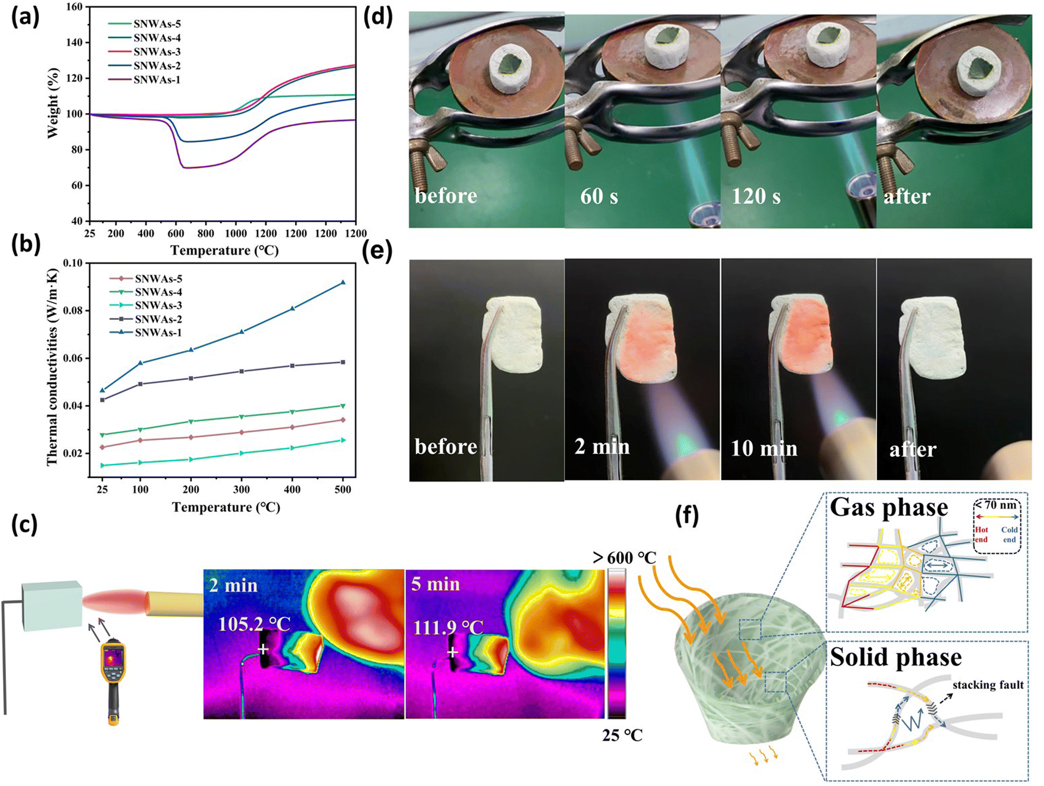 | ||
| Fig. 6 (a) TG curves and (b) thermal conductivities of the prepared samples. (c) Infrared thermal images of the temperature gradient for SNWAs-3 with a thickness of 2 cm under a butane blowtorch. (d) Optical images of a leaf placed on the SNWAs-3 under butane blowtorch flame treatment for different durations. (e) Optical images of the SNWAs-3 after butane blowtorch flame treatment for different durations. (f) Schematic illustration of the heat transfer mechanism of the SNWAs. | ||
Subsequently, the masses of the prepared SNWAs gradually stabilize when the temperature is kept at 1200 °C for 2 h. This is because the formation of an amorphous oxide layer (SiO2) on the surface of SiC nanowires can protect the SiC nanowires from further oxidation. After the test, the masses of the SNWAs-1, SNWAs-2, SNWAs-3, SNWAs-4 and SNWAs-5 are determined to increase by 34.11%, 25.89%, 26.65%, 26.04% and 10.12%, respectively. It should be noted here that the mass-gain behavior of the SNWAs-5 with the highest amorphous SiO2 content is weaker than that of SNWAs-3. However, SNWAs-5 possesses poorer high-temperature stability than that of SNWAs-3. As shown in Fig. S5,† SNWAs-5 possesses many amorphous SiO2 blocks in the SiC nanowire network structure, after being oxidized in air, and the oxidized and thickened nanowires are connected with these amorphous silica blocks. Thus, the pore structure is apparently destroyed, and it can be predicted that the thermal insulation performance of the sample will reduce significantly.
Furthermore, the thermal conductivity performance of the prepared samples was studied. Specifically, the temperature-dependent thermal conductivities of the SNWAs were recorded over the temperature range from 25 to 500 °C (Fig. 6b). Notably, SNWAs-3 exhibits a thermal conductivity of 0.0149 W m−1 K−1 at room temperature (25 °C), which is much lower than that of SNWAs-1 (0.0463 W m−1 K−1), SNWAs-2 (0.0425 W m−1 K−1), SNWAs-4 (0.0278 W m−1 K−1) and SNWAs-5 (0.0226 W m−1 K−1). Clearly, with increasing the TEOS concentration from 0.1 M to 0.167 M, the thermal conductivity of the SNWAs gradually decreases, due to the disappearance of the unreacted thermally conductive carbon, which is a result of the incomplete transformation of BCTs. In contrast, with further increasing the TEOS concentration from 0.167 M to 0.5 M, the thermal conductivity of the SNWAs in turn increases because the presence of bulk amorphous SiO2 reduces the porosity of the aerogels and ultimately enhances their solid-state thermal conductivity. These results comprehensively suggest the great potential of SNWAs-3 being used as a thermal insulation material. To further demonstrate the superiority of the SNWAs, we compare their thermal conductivities with those of recently reported porous ceramics, demonstrating their better performance (Fig. S6†). Such ultra-low thermal conductivity of SNWAs-3 can be attributed to the strong boundary scattering generated by the 3D network of SiC NWs as well as the enhanced light defect scattering attributed to stacking faults in SiC nanowires.22 More interestingly, the thermal conductivity of SNWAs-3 at 500 °C is found to be as low as 0.0256 W m−1 K−1, demonstrating its excellent high-temperature insulation performance.
After confirming the thermal insulation properties of the SNWAs-3, we evaluated its transient temperature behavior via an infrared temperature camera. As shown in Fig. 6c, on directly exposing the right end of the 2 cm thick sample to burning with a butane flame, it reached temperatures as high as 1300 °C, while the maximum temperature of the left surface was kept at around 111.9 °C after 5 min of direct contact with the butane flame. To further demonstrate the thermal insulation performance, a fresh leaf was placed on the top of a 2 cm thick SNWAs-3 sample, while heating it with a butane flame underneath. As displayed in Fig. 6d, the leaf remains fresh without carbonization after heating for 120 s, highlighting the excellent thermal insulation behavior of SNWAs-3. More importantly, the macroscopic shape and color of the SNWAs-3 show negligible change after exposure to the butane blowtorch flame (∼1300 °C) for 10 min (Fig. 6e), indicating the superb ablation resistance and thermal stability of SNWAs-3. Therefore, it can be confirmed that the SNWAs-3 possesses both high-temperature resistance and excellent thermal insulation properties.
Based on the above results, the heat transfer mechanism over the SNWAs can be proposed and this is illustrated in Fig. 6f. Typically, two mechanisms occurred on the SNWAs including gas and solid phase heat conduction. Typically, the gas phase heat conduction is mainly affected by the porosity of the material.31–33 Air in the pores can be regarded as the dispersed phase in the aerogel, and the thermal conductivity (K) can be calculated according to the following equation:34
| K = Kc (1 − φd)/(1 + φd/2) ≈ Kc (1 − φd), |
| K = KPh + Ke, |
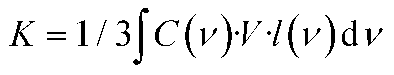
where KPh is the phonon thermal conductivity, Ke is the electron thermal conductivity, C(ν) is the specific heat capacity of the sample, ν is the phonon vibration frequency of the sample, l(ν) is the average free path of phonons and V is the volume of the sample. Given that the SiC nanowires are covalently bonded by Si–C in SNWAs-3, only scarce numbers of free electrons can impact its solid-phase thermal conductivity. Therefore, the phonon vibrations in the lattice wave play a dominant role in the heat transfer of SNWAs-3.38 At low temperatures, phonons in SNWAs have long wavelengths, making it easier to bypass defects without scattering, and thus the phonon scattering mainly occurs at the interface of SNWAs. As the temperature rises, the density of phonons in SNWAs also increases, which results in the higher possibility of phonon collisions and the free paths of phonons decrease greatly. The phonon scattering on defects and phase boundaries of the sample is still limited. Taken together, excellent gas- and solid–phase thermal conductivity of the SNWAs demonstrates its high potential for thermal insulation applications.
Considering practical applications in high-temperature oxidizing environments, the thermal insulation of SNWAs-3 during high-temperature oxidation was also investigated. In a typical test, the SNWAs-3 was calcined at 1200 °C for 2 h under an air atmosphere. As shown in Fig. 7a and b, the network structure constructed by SiC nanowires is maintained after high-temperature ablation, but the diameter of the fiber increased significantly. The TEM image shows the partial transformation of the SiC nanowires into SiO2 (Fig. 7c and Fig. S7†), causing the increase in the fiber diameter. The formation of the amorphous SiO2 layer on the SiC nanowires can effectively suppress the inward diffusion of oxygen into the nanowires, thus protecting the SiC nanowires from further oxidation. In addition, another typical morphology was observed, as shown in Fig. S6,† revealing that heterogeneous nanofibers consisting of amorphous SiO2 and SiC with numerous stacking faults play key roles in obstructing heat transfer and reinforcing the nanowire skeleton. Furthermore, an additional XRD peak attributed to SiO2 can be found in Fig. 7d, further confirming the formation of SiO2 on the surface of SiC. The formation of the SiO2 layer can be also confirmed by the FTIR characterization, where three absorption bands at 1094, 779 and 480 cm−1 assigned to Si–O can be observed (Fig. 7e).39 Furthermore, there are also two new characteristic peaks observed at 478 and 558 cm−1 in the Raman spectrum of the SNWAs-3 after calcination at 1200 °C, attributed to the bending motion and stretching vibration of the Si–O bond, respectively (Fig. S8†).40 The valence state and chemical composition of the SNWAs-3 after calcination at 1200 °C were further investigated by XPS. As shown in Fig. 7f, the high-resolution Si 2p XPS spectrum of SNWAs-3 after calcination at 1200 °C displays two peaks at 100.7 eV and 102.7 eV corresponding to Si–C and Si–O bonds, respectively. Similarly, the characteristic peaks associated with the O–Si bond of the SiO2 nanolayer can also be observed in the high-resolution O 1s and C 1s XPS spectra.41 To study the recycling use of the SNWAs-3 after calcination at 1200 °C, the sample was retested. As shown in Fig. 7i, the thermal conductivity of the SNWAs-3 after calcination at 1200 °C is 0.0226 W m−1 K−1 at room temperature, and this was maintained at 0.046 W m−1 K−1 at 500 °C. It shows that SNWAs-3 still has a very low thermal conductivity after high-temperature ablation, indicating that SNWAs-3 holds great promise for practical applications. To demonstrate the superiority of our biomass-template methods for the preparation of thermal insulation materials, other biomass materials such as Pleurotus eryngii fungus and gourds are also employed as the carbon templates for the preparation of SNWAs. Surprisingly, SiC nanowire aerogels with similar morphology can be also obtained (Fig. S9 and S10†). Obviously, this biomass template process can be a universal method for the preparation of SiC ceramic aerogels with superior thermal insulation performance.
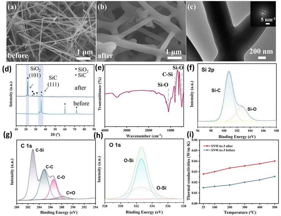 | ||
| Fig. 7 SEM images of SNWAs-3 before (a) and after (b) thermal treatment at 1200 °C for 2 h in air. (c) TEM image of SNWAs-3 after thermal treatment at 1200 °C for 2 h in air, and the corresponding SAED pattern (inset). (d) XRD patterns of SNWAs-3 before and after thermal treatment at 1200 °C for 2 h in air. (e) FTIR spectra after thermal treatment at 1200 °C for 2 h in air. High-resolution Si 2p (f), C 1s (g) and O 1s (h) XPS spectra for the SNWAs-3 after thermal treatment at 1200 °C for 2 h in air. (i) Thermal conductivities of SNWAs-3 under different temperatures before and after thermal treatment at 1200 °C for 2 h in air. | ||
4. Conclusions
In summary, we have reported a facile and versatile method for the preparation of SiC aerogels for thermal insulation applications. Specifically, we employed a biomass-derived carbon method for the preparation of SiC nanowire aerogels with 3D interconnected structures. The optimized SNWAs demonstrate low gas- and solid-phase thermal conductivity due to their abundant porous and stacking fault-connected SiC nanowire structure. In addition, the partial transformation of SiC into SiO2 under elevated temperatures can prohibit the SiC nanowires from further oxidation, resulting in enhanced thermal insulation performance. As a result, the optimized SNWAs show exceptionally low thermal conductivity, when measured at room temperature (0.0149 W m−1 K−1) and 500 °C (0.0256 W m−1 K−1). More interestingly, such an excellent performance of the SNWAs can be preserved after exposure to air at 1200 °C for 2 h, showing a low thermal conductivity of 0.0226 W m−1 K−1. These features ensure the suitability of the prepared SNWAs for long-term applications. These findings demonstrate a highly effective and low-cost approach for the preparation of SiC aerogels towards thermal insulation applications.Author contributions
Xinyang Li and Xiaoye Hu designed the experiment. Chunxue Zheng finished the fabrication and characterization of materials. Jie Yu analyzed the corresponding results. Zhulin Huang, Ming Li and Yue Li reviewed and edited the manuscript. All authors reviewed the results and approved the final version of the manuscript.Conflicts of interest
The authors declare no competing financial interest.Acknowledgements
This work was financially supported by the National Natural Science Foundation of China (Grant No. 52222208, 52072373, and 21673245), China National Funds for Distinguished Young Scientists (Grant No. 51825103), Major Science and Technology Project of Anhui Province (Grant No. 008192841048), and HFIPS Director's Fund (Grant No. BJPY2021B04, YZJJ202202-CX, YZJJ202312-TS, YZJJ202308-TS, YZJJ2022QN28, and YZJJ202401-TS).References
- J. T. Cahill, S. Turner, J. Ye, B. Shevitski, S. Aloni, T. F. Baumann, A. Zettl, J. D. Kuntz and M. A. Worsley, Chem. Mater., 2019, 31, 3700–3704 CrossRef CAS.
- E. Zhang, W. Zhang, T. lv, J. Li, J. Dai, F. Zhang, Y. Zhao, J. Yang, W. Li and H. Zhang, ACS Appl. Mater. Interfaces, 2021, 13, 20548–20558 CrossRef CAS PubMed.
- S. Guo, J. Am. Ceram. Soc., 2018, 101, 2707–2711 CrossRef CAS.
- A. Emmerling, J. Gross, R. Gerlach, R. Goswin, G. Reichenauer, J. Fricke and H.-G. Haubold, J. Non-Cryst. Solids, 1990, 125, 230–243 CrossRef CAS.
- D. Huang, C. Guo, M. Zhang and L. Shi, Mater. Des., 2017, 129, 82–90 CrossRef CAS.
- A. Emmerling, J. Gross, R. Gerlach, R. Goswin, G. Reichenauer, J. Fricke and H. G. Haubold, J. Non-Cryst. Solids, 1990, 125, 230–243 CrossRef CAS.
- Z.-L. Yu, N. Yang, V. Apostolopoulou-Kalkavoura, B. Qin, Z.-Y. Ma, W.-Y. Xing, C. Qiao, L. Bergström, M. Antonietti and S.-H. Yu, Angew. Chem., Int. Ed., 2018, 57, 4538–4542 CrossRef CAS PubMed.
- R. Saliger, T. Heinrich, T. Gleissner and J. Fricke, J. Non-Cryst. Solids, 1995, 186, 113–117 CrossRef CAS.
- X. Wu, W. Li, G. Shao, X. Shen, S. Cui, J. Zhou, Y. Wei and X. Chen, Ceram. Int., 2017, 43, 4188–4196 CrossRef CAS.
- J. Ma, F. Ye, C. Yang, J. Ding, S. Lin, B. Zhang and Q. Liu, Mater. Des., 2017, 131, 226–231 CrossRef CAS.
- Z. Hu, J. He, X. Li, H. Ji, D. Su and Y. Qiao, J. Porous Mater., 2017, 24, 657–665 CrossRef CAS.
- W. Kang, J. Chen, Y. Zhang, Q. Zhang, T. Chen and Y. Gou, J. Mater. Res. Technol., 2023, 23, 1559–1569 CrossRef CAS.
- Z. Wang, H. Zhao, D. Dai, H. Hao and Z. Wang, Ceram. Int., 2022, 48, 26416–26424 CrossRef CAS.
- Z. Wang, Y. Hou, H. Hao, Y. Shuai and Z. Wang, Carbon, 2023, 211, 118092 CrossRef CAS.
- Z. Wang, J. Liu, H. Hao, Q. Jing, S. Yan, J. Guo and Z. Wang, Carbon, 2024, 217, 118622 CrossRef CAS.
- L. Su, H. Wang, M. Niu, X. Fan, M. Ma, Z. Shi and S.-W. Guo, ACS Nano, 2018, 12, 3103–3111 CrossRef CAS PubMed.
- L. Song, F. Zhang, Y. Chen, L. Guan, Y. Zhu, M. Chen, H. Wang, B. R. Putra, R. Zhang and B. Fan, Nano-Micro Lett., 2022, 14, 152 CrossRef CAS PubMed.
- S. Li, H. Li, Q. Su, X. Liu, H. Zhao, M. Ding, K. Liu and W. Nie, Mater. Lett., 2017, 199, 113–115 CrossRef CAS.
- J. Zhu, J. Jia, F.-l. Kwong and D. H. Ng, Diamond Relat. Mater., 2013, 33, 5–11 CrossRef CAS.
- M. IslamRaja, C. Chang, J. McVittie, M. Cappelli and K. Saraswat, J. Vac. Sci. Technol., B: Microelectron. Nanometer Struct.–Process., Meas., Phenom., 1993, 11, 720–726 CrossRef CAS.
- Y. Chen, O. Ola, G. Liu, L. Han, M. Z. Hussain, K. Thummavichai, J. Wen, L. Zhang, N. Wang and Y. Xia, J. Eur. Ceram. Soc., 2021, 41, 3970–3979 CrossRef CAS.
- Y. Yu, C. Zhou, S. Zhang, M. Zhu, M. Wuttig, C. Scheu, D. Raabe, G. J. Snyder, B. Gault and O. Cojocaru-Mirédin, Mater. Today, 2020, 32, 260–274 CrossRef CAS.
- M. Han, X. Yin, W. Duan, S. Ren, L. Zhang and L. Cheng, J. Eur. Ceram. Soc., 2016, 36, 2695–2703 CrossRef CAS.
- Y. Yuan, Y. Ding, C. Wang, F. Xu, Z. Lin, Y. Qin, Y. Li, M. Yang, X. He, Q. Peng and Y. Li, ACS Appl. Mater. Interfaces, 2016, 8, 16852–16861 CrossRef CAS PubMed.
- J. Chen, Q. Shi and W. Tang, Mater. Chem. Phys., 2011, 126, 655–659 CrossRef CAS.
- A. Tadjarodi, M. Haghverdi and V. Mohammadi, Mater. Res. Bull., 2012, 47, 2584–2589 CrossRef CAS.
- M. Zhang, H. Lin, S. Ding, T. Wang, Z. Li, A. Meng, Q. Li and Y. Lin, Composites, Part B, 2019, 179, 107525 CrossRef CAS.
- L. Su, H. Wang, M. Niu, S. Dai, Z. Cai, B. Yang, H. Huyan and X. Pan, Sci. Adv., 2020, 6, eaay6689 CrossRef CAS PubMed.
- M. Bechelany, A. Brioude, D. Cornu, G. Ferro and P. Miele, Adv. Funct. Mater., 2007, 17, 939–943 CrossRef CAS.
- G. Zu, T. Shimizu, K. Kanamori, Y. Zhu, A. Maeno, H. Kaji, J. Shen and K. Nakanishi, ACS Nano, 2018, 12, 521–532 CrossRef CAS PubMed.
- S. Zhang, L. Wang, J. Feng, Y. Jiang, L. Li and J. Feng, ACS Appl. Nano Mater., 2023, 6, 10511–10520 CrossRef CAS.
- X. Zhang, X. Cheng, Y. Si, J. Yu and B. Ding, ACS Nano, 2022, 16, 5487–5495 CrossRef CAS PubMed.
- Y. Li, X. Liu, X. Nie, W. Yang, Y. Wang, R. Yu and J. Shui, Adv. Funct. Mater., 2019, 29, 1807624 CrossRef.
- S. Tian, Material physical properties, Beihang University Press, 2001, vol. 5, pp. 258–270 Search PubMed.
- A. Du, H. Wang, B. Zhou, C. Zhang, X. Wu, Y. Ge, T. Niu, X. Ji, T. Zhang, Z. Zhang, G. Wu and J. Shen, Chem. Mater., 2018, 30, 6849–6857 CrossRef CAS.
- V. Apostolopoulou-Kalkavoura, P. Munier and L. Bergström, Adv. Mater., 2021, 33, 2001839 CrossRef CAS PubMed.
- L. Li, C. Jia, Y. Liu, B. Fang, W. Zhu, X. Li, L. A. Schaefer, Z. Li, F. Zhang and X. Feng, Mater. Today, 2022, 54, 72–82 CrossRef CAS.
- X. Qian, J. Zhou and G. Chen, Nat. Mater., 2021, 20, 1188–1202 CrossRef CAS PubMed.
- L. Su, H. Wang, M. Niu, S. Dai, Z. Cai, B. Yang, H. Huyan and X. Pan, Sci. Adv., 2020, 6, eaay6689 CrossRef CAS PubMed.
- C. Wang, Z. Fang, A. Yi, B. Yang, Z. Wang, L. Zhou, C. Shen, Y. Zhu, Y. Zhou and R. Bao, Light: Sci. Appl., 2021, 10, 139 CrossRef CAS PubMed.
- K. Peng, J. Zhou, H. Gao, J. Wang, H. Wang, L. Su and P. Wan, ACS Appl. Mater. Interfaces, 2020, 12, 19519–19529 CrossRef CAS PubMed.
Footnote |
| † Electronic supplementary information (ESI) available. See DOI: https://doi.org/10.1039/d3nr06076d |
| This journal is © The Royal Society of Chemistry 2024 |