 Open Access Article
Single gold nanowires with ultrahigh (>104) aspect ratios by triphasic electrodeposition†
Guillermo
Colón-Quintana
a,
Thomas B.
Clarke
 a,
Sakshi A.
Ailawar
 a and
Jeffrey E.
Dick
 *ab
*ab
aDepartment of Chemistry, Purdue University, West Lafayette, IN 47907, USA. E-mail: jdick@purdue.edu
bElmore School of Electrical and Computer Engineering, Purdue University, West Lafayette, IN 47907, USA
First published on 3rd September 2024
Abstract
Due to their superior optical and electrical properties, gold nanowires are used ubiquitously across industries. Current techniques for fabricating such structures are often expensive, involving multiple steps, cleanroom operation, and limited ability for a user to controllably place a nanowire at a desired location. Here, we introduce the concept of triphasic electrodeposition, where metal salts act as antagonistic salts at the liquid|liquid interface, leading to their increased concentration at this phase boundary. We show that the electrodeposition of ultra-high aspect ratio gold nanowires may be achieved in a one-step, one-pot method by submerging a conductor in contact with two phases: an organic phase containing HAuCl4 and a quaternary ammonium salt, and an aqueous phase containing potassium chloride. Changing electrodeposition parameters in the triphasic system allows tunability of important features of the nanowire, such as size and thickness. Furthermore, this new method provides an impressive ability to choose the geometry and precise positioning of deposited nanowires simply by changing where a liquid|liquid interface contacts the electrode surface.
Since its discovery, humans have been attracted to gold and its unique properties. Its high chemical stability, electrical conductivity, and malleability have made it a prime candidate for use in various domains, from technology and currency to healthcare and aesthetics.1 Noteworthy examples include the use of gold in microprocessor development for increased computational capabilities and in biosensing and treatment, with early known uses of gold colloid solutions for treating diverse ailments and poisons dating back to the 5th century BCE.1,2 More recent examples of gold in medicine include the use of gold nanomaterials in biosensing and bioimaging applications, as drug, gene, or protein carriers, and as phototherapeutic agents.3,4
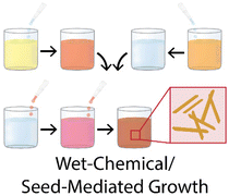
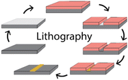
Within the last decade, there has been an outstanding interest in studying gold nanomaterials, mostly due to their unique properties over their macro counterparts. Although nanoparticles are one of the most employed geometries, many other geometries, including nanorods and nanowires, have also shown outstanding physical and chemical properties. Nanowires, for example, have shown remarkable growth in electronics, energy conversion and storage, catalysis, optics, and biosensing.5–16 Gold nanowires have especially been shown to hold many advantages in biosensing and electronics due to their composition, such as being chemically unreactive, electrically conductive, and biocompatible.16–23 For example, gold nanowires have previously been used with surface-enhanced Raman spectroscopy (SERS), where the enhanced electromagnetic field has been shown to amplify Raman signals of adsorbed molecules and enable ultrasensitive detection.23 However, most conventional synthesis methods for such nanowires are limited to chemical reductions of metal precursors, seed-mediated growth, template-assisted synthesis, or other lithographic methods that require clean rooms or specialized instrumentation (see Table 1).15,19,21,24–26,41,42
| Method | Ref. # | Reported lengths | Reported thicknesses | Reported aspect ratios | Able to make single nanowires? | Position control? |
|---|---|---|---|---|---|---|
|
19 | 10 μm | 16–66 nm | 200 | No | No |
| 29 | 355.3 ± 31.3 nm | 18.7 nm | 19 | No | No | |
| 30 | 16 ± 3 nm | N/A | 18 ± 2.5 | No | No | |
| 35 | 0.2–1.2 μm | N/A | 6–22 | No | No | |
| 40 | 400–500 nm | 19–20 nm | 21–23 | No | No | |
| 21 | ≤25 μm | 23–54 nm | 229–352 | No | No | |

|
34 | 389 ± 190 nm | 99 ± 24 nm | 15.7 ± 9.3 | No | No |

|
20 | 6 μm | 200–350 nm | 17–30 | No | Yes |
| 27 | 17–50 μm | 40–200 nm | 85–750 | No | No | |
| 28 | 55 μm | 15–20 nm | Avg = 4200 | No | No | |
| 39 | 10 μm | 1.7 ± 0.3 nm | 1000 | No | No | |
|
26 | 2.7 cm | 40 nm | 600![[thin space (1/6-em)]](https://www.rsc.org/images/entities/char_2009.gif) 000 000 |
Yes | Yes |
| 43 | 4600 nm | 150 nm | 31 | Yes | Yes | |
|
This work | 1.2 mm or longer | 80–100 nm | 12![[thin space (1/6-em)]](https://www.rsc.org/images/entities/char_2009.gif) 000 000 |
Yes | Yes |
Chemical synthesis methods, for example, have recently shown great potential for high aspect ratio nanowire synthesis.19,27–31 In the work of Khanal et al., the authors show a one-step synthesis for high aspect ratio nanowires using gold nanorod seed particles.21 This method had limitations: for instance, the method requires pre-existing nanorod seeds and strong acidic conditions, and it is also difficult to produce a homogenous size distribution of nanowires. Furthermore, with increasing interest in studying the physicochemical properties of nanomaterials,32 especially at the single entity level,33 such chemical synthesis methods are largely incapable of forming individual nanowires for analysis. Electrochemical seed-mediated methods exist, wherein the chemical reducing agent traditionally used in chemical seed-mediated growth is replaced/supplemented with an electrode held at a reducing potential.34,35 This methodology has been used to create micron-long nanowires with moderate aspect ratios, but often other shorter nanorods or nanoparticles are produced alongside these nanowires (i.e., there is poor control over the nano-geometry synthesized and location of such nanowires). Penner's group has introduced what they call the “electrochemical step edge decoration” methodology36 where various metals37,38 have been shown to preferentially electrodeposit at defects of an electrode material. However, this method is limited in that all step edge sites across the electrode will be the nucleation sites for nanowires, and precise localization (especially on basal planes) for a single nanowire is currently impossible unless an electrode is carefully engineered to exhibit one such step edge. In the methodology presented herein, one can specifically create a nanowire wherever on an electrode surface, simply by placing a liquid|liquid boundary at the desired location. Other methods of nanowire deposition, like those discussed by Menke et al., rely on using lithography to form gold nanowires, wherein a complex seven-step synthesis process was required to obtain high aspect ratios and control over nanowire thickness and length.26Table 1 provides a comparison between the techniques discussed herein. While homogeneous chemical or heterogeneous electrochemical methods offer a relatively simple protocol for the synthesis of gold nanowires and lithography provides impressive spatial and size control, no technique as of now simultaneously offers the ease and ability to precisely control the size, position, and number of nanowires produced.
Given the technological importance of gold nanowires, new methods are necessary to fabricate single gold nanowires with control over the nanowire's placement without complex lithographic techniques. While electrodeposition presents a relatively simple and cheap means of creating nanowires, to our knowledge it has not been reported before the present article for an electrodeposition technique alone to grow just one single nanowire at a time with control over the nanowire length, thickness, and placement on a larger substrate electrode. Instead, procedures rely on an additional step (e.g., patterning a surface with electrolyte channels)25 or other templated growth or lithographic pre-treatment (see Table 1) to expose regions for electrodeposition.
Our group has been studying electrochemistry under complex, multiphase conditions, where the three-phase boundary between two immiscible liquids and an electrode surface have shown interesting electrochemical properties.44–48 We have also shown that antagonistic salts can form under multiphase conditions, emulsifying the liquid|liquid interface because of interfacial solute flux.49
Here, we demonstrate a novel method (triphasic electrodeposition) for the electrodeposition of gold nanowires, with control over wire thickness, length, and size. This level of control was achieved using a combination of both multipotential chronoamperometric steps and a multiphase system involving an aqueous phase (top layer) and an oil phase (bottom layer) solution consisting of a non-aqueous electrolyte (tetrabutylammonium perchlorate, i.e., [NBu4][ClO4]) and a gold precursor ion (chloroaurate). We propose that these species interact and allow for the formation of an antagonistic salt that can adsorb to a liquid|liquid boundary, increasing the probability of gold nanowire nucleation and growth at the three-phase boundary. While others have reported the preferential electrodeposition of materials like silicates50 and polymers51,52 at three-phase boundaries, these strategies depend on confining the reactants, precursors, and/or catalysts to opposite phases, such that the reaction proceeds only where the two phases meet at the electrode surface. The strategy presented here offers a new methodology, where the precursor is confined within one phase and takes advantage of adsorption phenomena to achieve the preferential electrodeposition at the phase boundary. Notably, the aforementioned strategy of keeping reactants in separate phases has not enabled metal nanowire deposition at the boundary; however, Kaminska et al.53 used a very similar setup to that presented here, but only deposited gold nanoparticles at a liquid|liquid|electrode interface. Our optimized methodology allows one to produce single, millimeter-long nanowires in a single step without using a template or a clean room, requiring less gold precursor salt than most pre-existing lithographic methods.
Results
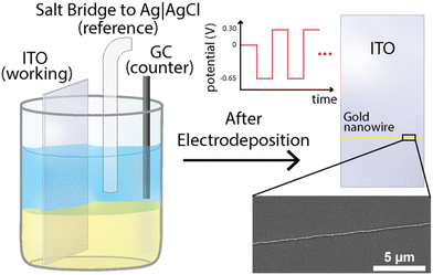
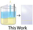
Fig. 1 shows this work's experimental setup and a full description of the methods are presented in the “Materials and methods” section of the ESI.† In short, a three-phase (liquid|liquid|solid) system was employed for the electrodeposition of gold nanowires. This system consisted of an aqueous top layer containing an aqueous salt (1 M KCl), an organic (1,2-dichloroethane (DCE)) bottom layer containing a non-aqueous electrolyte ([NBu4][ClO4]) with a gold precursor (HAuCl4), and a solid conductive phase (here an indium–tin oxide (ITO) working electrode was used). Both solutions were carefully pipetted into a container to prevent mixing, allowing for a clear and distinct phase boundary to form. The indium–tin oxide working electrode was then submerged through both the aqueous and organic phases ensuring adequate contact with both phases. A standard three-electrode setup was used, where the reference and counter consisted of an Ag|AgCl (1 M KCl) electrode and a glassy carbon rod (r = 1 mm), respectively, as shown in Fig. 1.To investigate the triphasic electrodeposition of gold, a sufficiently negative potential was applied to drive the electrodeposition of gold. In prior work,54 our group has shown the use of multi-step electrodeposition methods for the deposition of gold nanoring arrays and studied the effect of the potentials, time held at each potential, and number of deposition cycles, with results showing a clear correlation between gold-ring thickness and deposition time, concentration, overpotential, and number of cycles. In the experiments presented here, the same deposition conditions and parameters were sufficient to deposit high aspect ratio gold nanowires from this triphasic setup as well. Namely, the potential was systematically stepped, starting at −0.65 V for 0.5 seconds, followed by a second period at 0.3 V for 0.5 seconds, as shown in Fig. 1. This potential cycle was repeated throughout the experiment and varied to test for changes in deposition behavior. Following the deposition process, the ITO working electrode was removed from the DCE solution and immersed in deionized water for a minimum of 5 minutes to ensure the complete removal of any remaining precipitated supporting electrolyte or precursor chloroauric salt. The electrodes were subsequently submerged in acetone to remove excess water and leftover oils, and then pure DCE, with intermittent rinses using acetone. The resulting nanowire can be observed using a scanning electron microscope (SEM), as seen in Fig. 1 (inset). The chronoamperometric deposition allowed for the formation of firmly attached gold deposits with wire geometries. Fig. 2 presents further scanning electron microscopy images for the electrode surface after the deposition. The presence of gold was verified using energy-dispersive X-ray spectroscopy (EDX) analysis, as shown in Fig. S1.† Notably, gold is strongly confined to the three-phase interface but can sometimes be detected as small nanoparticles within a couple microns of the gold nanowires on the DCE side (see Fig. S1 and Table S1†). No gold was detected on the aqueous side of the three-phase boundary. Additionally, no gold wire deposition was observed when either the chloroaurate species or the quaternary ammonium salt was absent in this system.
The ability to adjust the width of these deposited nanowires is of great importance due to the distinctive properties exhibited by nanomaterials at this scale. By using chronoamperometry, we pulsed the potential and allowed for the nucleation of nanoparticles near/at the liquid|liquid boundary and growth to form nanowires along this three-phase boundary. Various experimental factors, including the potential applied during the deposition, the duration of the potential pulse process, and the number of repetitions that a potential pulse is employed, can significantly impact the thickness of the nanowires. Fig. 3 shows the influence of the repetition of chronoamperometric cycles on the deposition of gold nanowires. Here we show that as the number of cycles increases, from one to ten cycles, so does the width of the nanowire increase in size by a couple hundred nanometers. Fig. 3A, for example, shows a gold wire with a width of approximately 100 nm at its widest point, while Fig. 3D shows a nanowire whose width is slightly larger than 500 nm throughout. Fig. S2† shows an example current vs. time trace for one of these multi-cycle depositions. To further assess the dimensions of the nanowires, we took SEM images at different sample angles, including at 45°, so that an estimation of the height of the nanowires could be made. Fig. S3† shows that for a nanowire that was deposited with a width of ∼180 nm, the height of the same nanowire was approximately 200 nm, indicating that the nanowires can be quite hemicylindrical.
An additional discovery or application may be found in the fact that the movement of the working electrode between chronoamperometry cycles yields the ability to deposit multiple nanowires on the same electrode, as shown in Fig. 4 and Fig. S4.† This is possible because the three-phase boundary formed at the interface of our ITO working electrode and the liquid|liquid boundary can repeatedly be moved by changing the working electrode position. By changing the position of the working electrode in a vertical direction (as shown in Fig. 4A), one can then procedurally electrodeposit nanowires in a stepwise fashion. Like that of roads on a highway, different “lanes” can be generated by successive movement and deposition steps. Fig. 4B below shows an optical micrograph after three electrode movements and electrodeposition steps. These three distinct steps yield three separate nanowires based on the locations of the prior positions of the liquid|liquid interface (see Fig. S4†). Scanning electron microscopy images of increasing magnification can be observed in Fig. 4D and E. One notable observation from Fig. 4 is that of the high aspect ratios (length/width) that can be obtained for the wires produced here, with the relative thickness of ∼100 nm (shown in Fig. 3A, B and 4D) but relative lengths of the nanowires on the scale of millimeters in length, as shown in Fig. S4A and S4B.†Fig. 4B shows the presence of wires of 2 mm in length, with the most truly continuous segments for this specific horizontal wire spanning 800 μm in length without breakage. Examples for long length wires can be seen in Video S1,† wherein continuous microwires of up to 2 cm can be seen to be deposited with similar aspect ratios by tuning deposition conditions. These results highlight the technique's simplicity and its ability to place nanowires in a desired location by simply changing the placement of the three-phase boundary.
Notably, as the electrodeposition of the nanowire depends on the positioning and shape of the three-phase boundary formed at the interface of our ITO working electrode and the liquid|liquid boundary, one can deposit nanowires in varied geometries. Fig. S5,† for example, shows evidence of the ability to form continuous nanowires along the boundary of a pipetted droplet on an ITO electrode surface. Fig. S5A† shows a schematic representation of the system under question, where the glassy carbon rod counter and the Ag|AgCl (1 M KCl) reference electrode are positioned into an aqueous (1 M KCl) bulk solution surrounding a droplet of 10 mM HAuCl4 in 1,2-dichloroethane (DCE) solution containing 100 mM [NBu4][ClO4]. Similar to the procedure described above for the electrodeposition of other nanowires, a series of chronoamperometric potential steps are performed, starting with a −0.65 V vs. Ag|AgCl (1 M KCl) for 0.5 s step followed by another 0.5 s step at 0.3 V vs. Ag|AgCl (1 M KCl). The resulting behavior can be observed in Fig. S5(B–D),† where differences can be observed when comparing before (Fig. S5(B)†) and after (Fig. S5(C)†) deposition has taken place at/near the edge of the droplet. Fig. S5(D)† shows the residual nanowire after electrodeposition and after the droplet has been removed from the electrode surface.
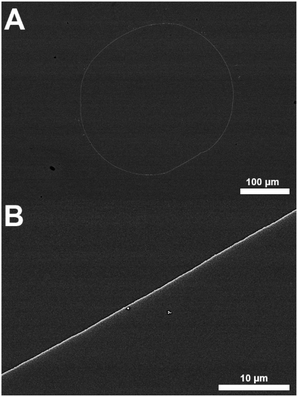
Fig. 5A and B shows a micrograph image taken with SEM after deposition using a droplet system, as described in Fig. S5.† Here, a continuous gold nanowire can be observed where the DCE droplet was positioned on the ITO. The diameter of the gold nanowire ring measures approximately 376 μm in diameter equating to a circumference of 1.181 mm. Fig. 5A demonstrates that the electrodeposition can be carried out to maintain a consistent nanowire width with significant length. These images demonstrate the ability to accurately deposit large aspect ratio nanowires of different geometries based on the geometry of a three-phase system. These same wires may also be exfoliated from the electrode surface for use in other studies; Fig. S6† shows SEM micrographs of exfoliated wires taken from a droplet system using carbon tape. As can be noted from Fig. S6,† the act of exfolitating the nanowires induces several breaks and discontinuities in the wire, making an independent conductivity measurement of individual wires incredibly difficult. Therefore, relying on the circumference and thickness of wires estimated from SEM images shown in Fig. 5, the aspect ratio of this as-deposited ring-shaped wire, can be estimated to be on the order of 2 × 10⁴.
Increased control of nanowire geometry and positioning was additionally achieved by changing the geometry of the contacting oil phase in this three-phase system, as shown in Fig. S7† and Fig. 6. Here optical micrograph and scanning electron microscopy images show the use of capillaries for the controlled positioning of three-phase boundaries using two different capillary templates and subsequent deposition of nanowires along these geometries. Fig. S7A–S7C† and Fig. 6A–C show multiple optical micrographs of repeatable instances of shaped deposition for each case. “D” shaped nanowires achieved with a theta capillary can be seen in Fig. S7A–S7C,† while circular nanowires based on a regular glass capillary can be seen in Fig. 6A–D. To achieve this behavior capillary tubes were brought very close to our conductive ITO surface (already submerged in 1 M KCl) and subsequently filled with a 0.1 M [NBu4][ClO4] and 10 mM chloroauric acid solution. Upon filling the capillary, a liquid|liquid|electrode three-phase interface can be created (assuming the capillary is not fully contacting the ITO surface), from which a nanowire can be deposited as before. For example, a multipotential-step chronoamperometric method was then used for the deposition, using the same potentials for 2 cycles. To allow for multiple depositions of these shapes on the same electrode, the capillaries were simply lifted from the surface after a deposition and repositioned slightly above the ITO again several hundred micrometers away laterally from the previous position using a micro-positioner. From here, the chloroauric acid solution was re-inserted into the capillary tube and the deposition steps were repeated. Fig. 6C shows two such circular nanowires deposited next to each other with the round capillary, while Fig. S7B and C† show multiple “D” shaped nanowires achieved with the theta capillary. The fact that these images show numerous gold nanowire shapes deposted close to one another suggests a strong degree of reproducibility and further demonstrates this system's control and ability to accurately deposit nanowires of desired geometries on conductive surfaces.
Discussion
We attribute the formation of nanowires to the increased concentration of AuCl4− at the interface between the liquid phases and not simply due to other reasons such as lower iR drop or double layer charging time at the three phase boundary. To refute these alternative explanations, we conducted a set of additional control experiments. In the first, we ensured that the glassy carbon counter electrode only had contact with the DCE phase (see Fig. S6†). Even in this configuration, preferential electroreduction of gold still occurs at the location where the water|DCE interface meets the ITO electrode. This suggests that the reason nanowires are formed is not solely because electrodeposition at the three-phase boundary is the path of least resistance, since no ion transfer across the liquid|liquid interface is necessary when the counter electrode is confined to the DCE phase. Additionally, Fig. S7† shows a scanning electron micrograph wherein a larger overpotential is applied. Specifically, −0.9 V vs. the Ag|AgCl reference electrode was applied to the ITO electrode using the same experimental setup as shown in Fig. 1. Here, preferential electrodeposition of gold at the three-phase interface is still observed to occur at the three-phase boundary; however, additional deposition is observed throughout the ITO|DCE interface, suggesting that while nanoparticles are still able to be deposited from the bulk chloroaurate, the concentration there is insufficient to spontaneously grow nanoparticles at more mild potentials. Furthermore, nanowire formation with few-to-no nanoparticles being formed from the bulk DCE phase, was achieved when a constant potential of −0.65 V was applied for several seconds, which suggests that any difference in double layer charging time between the different interfaces is not solely responsible for this phenomenon.We therefore propose that the preferential electrodeposition is due to the formation of an antagonistic salt, [NBu4][AuCl4], from the original chloroaurate and tetrabutylammonium cations present in the DCE phase (eqn (1)).53,55 This antagonistic salt can then adsorb at the liquid|liquid boundary (i.e., the water|DCE interface) based on the difference in solubility of the two ions (eqn (2)).49,55 Then the reduction of chloroaurate present at the water|DCE interface can electrodeposit gold on the surface of the electrode (eqn (3)).
| AuCl4− (DCE) + NBu4+ (DCE) ↔ [NBu4][AuCl4] (DCE) | (1) |
| [NBu4][AuCl4] (DCE) ↔ [NBu4][AuCl4] (DCE|aq.) | (2) |
| [NBu4][AuCl4] (DCE|aq.) + e− → Au(s) + 4 Cl− (DCE) + NBu4+ (DCE) | (3) |
Reaction (3) needs to be accompanied by an ion transfer reaction, as the current must flow between the working electrode (where a reactant from the dichloroethane phase – i.e., chloroaurate – is reduced) through the aqueous phase to the counter electrode where oxidation occurs. Therefore, either an anion from the dichloroethane phase needs to transfer to the aqueous phase or an aqueous cation transfers to the DCE phase. Given the ion transfer potentials of the ions that satisfy these conditions,56 the most likely ion transfer reaction is the generated chloride (from chloroaurate) into the aqueous phase. In fact, this could be a concerted reaction as shown by reaction (4):
| [NBu4][AuCl4] (DCE|aq.) + e− → Au(s) + 4 Cl− (aq.) + NBu4+ (DCE) | (4) |
Besides chloride transferring to the aqueous phase, the perchlorate anion is the next most thermodynamically favorable anion to transfer to the aqueous phase to maintain electroneutrality; whereas potassium transferring from the aqueous phase to the DCE phase is not spontaneous.56
Our group has previously studied the mechanism of this phenomenon.49 Importantly, the physico-chemical properties of our strategy differs from previously reported liquid|liquid chemical seed-mediated and electrochemical seed-mediated growth strategies. In the former, a chemical reductant can be placed in one liquid phase, where the other phase contains the metal precursor reactant. Only where the two phases meet can the metal be reduced, creating nanoparticles at the liquid|liquid. In the latter, the electrode replaces the chemical reductant as the source of electrons, and as such, nanoparticles, nanorods, and/or nanowires are deposited at many locations scattered across this electroactive surface. While in our methodology the electrode still acts as the electron source, we use the relative difference in solubilities between the organic cation and the anionic metal precursor to favor adsorption and increase the metal concentration at the liquid|liquid interface. This increases the probability of nucleation and subsequent growth of the nanowires at this three-phase interface. Others, like Liu et al., investigated the reduction of HAuCl4 through UV radiation and revealed that phthalocyanine derivative compounds with quaternary ammonium cations exhibited preconcentration at the liquid–air interface.57 Considering the presence of quaternary ammonium salts in the DCE phase of our experiments, a similar preconcentration of NBu4+ at the water–oil interface could potentially facilitate favorable interactions with AuCl4− at the interface, thereby promoting the deposition of gold nanowires. Given the interactions between the chloroaurate anion and the quaternary ammonium cation, an antagonistic salt could be forming and allowing for surfactant-like behavior to preferentially preconcentrate gold at the liquid|liquid|electrode interface allowing for electrodeposition of these high aspect ratio nanowires. While the generalizability of this technique is the topic of current study, we acknowledge that the chloroaurate anion may be especially able to achieve this type of triphasic electrodeposition due to its properties as an anionic metal complex that can ion pair with a tetraalkylammonium cation and have sufficient solubility in both the aqueous and organic phases.
Conclusion
In summary, we present a new concept, termed triphasic electrodeposition, for the electrodeposition of gold nanowires with ultrahigh aspect ratios, tunable thickness, length, positioning, and geometry. This nanowire electrodeposition is achieved by taking advantage of a three-phase boundary (liquid|liquid|electrode) and multipotential step chronoamperometric methods to preferentially deposit gold at the three-phase boundary. The work presented here shows a template-free and cleanroom-free method for forming mm-length nanowires with tunable aspect ratios and excellent control over nanowire placement on a conductive surface.Data availability
The data used in the paper is available either in the main text or in ESI.†Conflicts of interest
There are no conflicts to declare.Acknowledgements
We would like to acknowlege support from National Science Foundation CAREER under grant number CHE-2045672.References
- F. Habashi, Gold – An Historical Introduction, in Gold Ore Processing, ed. M. D. Adams, Elsevier, 2nd edn, 2016, pp. 1–20 Search PubMed.
- L. A. Dykman and N. G. Khlebstov, Gold Nanoparticles in Biology and Medicine: Recent Advances and Prospects, Acta Nat., 2011, 3(2), 34–55 Search PubMed.
- P. Si, N. Razmi, O. Nur, S. Solanki, C. M. Pandey and R. K. Gupta, et al., Gold nanomaterials for optical biosensing and bioimaging, Nanoscale Adv., 2021, 3(10), 2679–2698 Search PubMed.
- X. Hu, Y. Zhang, T. Ding, J. Liu and H. Zhao, Multifunctional Gold Nanoparticles: A Novel Nanomaterial for Various Medical Applications and Biological Activities, Front. Bioeng. Biotechnol., 2020, 8, 990 Search PubMed.
- M. Law, J. Goldberger and P. Yang, Semiconductor Nanowires and Nanotubes, Annu. Rev. Mater. Res., 2004, 34(1), 83–122 Search PubMed.
- W. E. Teo and S. Ramakrishna, A review on electrospinning design and nanofibre assemblies, Nanotechnology, 2006, 17(14), R89 Search PubMed.
- A. I. Hochbaum and P. Yang, Semiconductor Nanowires for Energy Conversion, Chem. Rev., 2010, 110(1), 527–546 Search PubMed.
- C. M. Lieber and Z. L. Wang, Functional Nanowires, MRS Bull., 2007, 32(2), 99–108 Search PubMed.
- S. Gong and W. Cheng, One-Dimensional Nanomaterials for Soft Electronics, Adv. Electron. Mater., 2017, 3(3), 1600314 Search PubMed.
- Q. Wei, F. Xiong, S. Tan, L. Huang, E. H. Lan and B. Dunn, et al., Porous One-Dimensional Nanomaterials: Design, Fabrication and Applications in Electrochemical Energy Storage, Adv. Mater., 2017, 29(20), 1602300 Search PubMed.
- L. N. Quan, J. Kang, C.-Z. Ning and P. Yang, Nanowires for Photonics, Chem. Rev., 2019, 119(15), 9153–9169 Search PubMed.
- G. T. Chandran, X. Li, A. Ogata and R. M. Penner, Electrically Transduced Sensors Based on Nanomaterials (2012–2016), Anal. Chem., 2017, 89(1), 249–275 Search PubMed.
- C. Jia, Z. Lin, Y. Huang and X. Duan, Nanowire Electronics: From Nanoscale to Macroscale, Chem. Rev., 2019, 119(15), 9074–9135 Search PubMed.
- P. Yang, R. Yan and M. Fardy, Semiconductor Nanowire: What's Next?, Nano Lett., 2010, 10(5), 1529–1536 Search PubMed.
- L. Soleimany, A. Dolati and M. Ghorbani, A study on the kinetics of gold nanowire electrodeposition in polycarbonate templates, J. Electroanal. Chem., 2010, 645(1), 28–34 Search PubMed.
- M. Kang, H. Lee, T. Kang and B. Kim, Synthesis, Properties, and Biological Application of Perfect Crystal Gold Nanowires: A Review, J. Mater. Sci. Technol., 2015, 31(6), 573–580 Search PubMed.
- Y. Xia, P. Yang, Y. Sun, Y. Wu, B. Mayers and B. Gates, et al., One-Dimensional Nanostructures: Synthesis, Characterization, and Applications, Adv. Mater., 2003, 15(5), 353–389 Search PubMed.
- B. Wu, A. Heidelberg and J. J. Boland, Mechanical properties of ultrahigh-strength gold nanowires, Nat. Mater., 2005, 4(7), 525–529 Search PubMed.
- F. Kim, K. Sohn, J. Wu and J. Huang, Chemical Synthesis of Gold Nanowires in Acidic Solutions, J. Am. Chem. Soc., 2008, 130(44), 14442–14443 Search PubMed.
- Y. Bahari Mollamahale, M. Ghorbani, A. Dolati and D. Hosseini, Electrodeposition of well-defined gold nanowires with uniform ends for developing 3D nanoelectrode ensembles with enhanced sensitivity, Mater. Chem. Phys., 2018, 213, 67–75 Search PubMed.
- B. P. Khanal and E. R. Zubarev, Gold Nanowires from Nanorods, Langmuir, 2020, 36(49), 15030–15038 Search PubMed.
- B. Zhu, S. Gong, F. Lin, Y. Wang, Y. Ling and T. An, et al., Patterning Vertically Grown Gold Nanowire Electrodes for Intrinsically Stretchable Organic Transistors, Adv. Electron. Mater., 2019, 5(1), 1800509 Search PubMed.
- E. Cara, L. Mandrile, F. Ferrarese Lupi, A. M. Giovannozzi, M. Dialameh and C. Portesi, et al., Influence of the long-range ordering of gold-coated Si nanowires on SERS, Sci. Rep., 2018, 8(1), 11305 Search PubMed.
- L. Liu, W. Lee, Z. Huang, R. Scholz and U. Gösele, Fabrication and characterization of a flow-through nanoporous gold nanowire/AAO composite membrane, Nanotechnology, 2008, 19(33), 335604 Search PubMed.
- M. Yun, N. V. Myung, R. P. Vasquez, C. Lee, E. Menke and R. M. Penner, Electrochemically Grown Wires for Individually Addressable Sensor Arrays, Nano Lett., 2004, 4(3), 419–422 Search PubMed.
- E. J. Menke, M. A. Thompson, C. Xiang, L. C. Yang and R. M. Penner, Lithographically patterned nanowire electrodeposition, Nat. Mater., 2006, 5(11), 914–919 Search PubMed.
- B. Wu and J. J. Boland, Synthesis and dispersion of isolated high aspect ratio gold nanowires, J. Colloid Interface Sci., 2006, 303(2), 611–616 Search PubMed.
- W. Xin, I. M. De Rosa, Y. Cao, X. Yin, H. Yu and P. Ye, et al., Ultrasonication-assisted synthesis of high aspect ratio gold nanowires on a graphene template and investigation of their growth mechanism, Chem. Commun., 2018, 54(33), 4124–4127 Search PubMed.
- H.-Y. Wu, W.-L. Huang and M. H. Huang, Direct High-Yield Synthesis of High Aspect Ratio Gold Nanorods, Cryst. Growth Des., 2007, 7(4), 831–835 Search PubMed.
- N. R. Jana, L. Gearheart and C. J. Murphy, Wet Chemical Synthesis of High Aspect Ratio Cylindrical Gold Nanorods, J. Phys. Chem. B, 2001, 105(19), 4065–4067 Search PubMed.
- G. A. Vinnacombe-Willson, Y. Conti, A. Stefancu, P. S. Weiss, E. Cortés and L. Scarabelli, Direct Bottom-Up In Situ Growth: A Paradigm Shift for Studies in Wet-Chemical Synthesis of Gold Nanoparticles, Chem. Rev., 2023, 123(13), 8488–8529 Search PubMed.
- M. A. Gatoo, S. Naseem, M. Y. Arfat, A. Mahmood Dar, K. Qasim and S. Zubair, Physicochemical Properties of Nanomaterials: Implication in Associated Toxic Manifestations, BioMed Res. Int., 2014, 2014(1), 498420 Search PubMed.
- L. A. Baker, Perspective and Prospectus on Single-Entity Electrochemistry, J. Am. Chem. Soc., 2018, 140(46), 15549–15559 Search PubMed.
- L. G. Abdelmoti and F. P. Zamborini, Potential-Controlled Electrochemical Seed-Mediated Growth of Gold Nanorods Directly on Electrode Surfaces, Langmuir, 2010, 26(16), 13511–13521 Search PubMed.
- Z. Wei, A. J. Mieszawska and F. P. Zamborini, Synthesis and Manipulation of High Aspect Ratio Gold Nanorods Grown Directly on Surfaces, Langmuir, 2004, 20(11), 4322–4326 Search PubMed.
- M. P. Zach, K. H. Ng and R. M. Penner, Molybdenum Nanowires by Electrodeposition, Science, 2000, 290(5499), 2120–2123 Search PubMed.
- M. P. Zach, K. Inazu, K. H. Ng, J. C. Hemminger and R. M. Penner, Synthesis of Molybdenum Nanowires with Millimeter-Scale Lengths Using Electrochemical Step Edge Decoration, Chem. Mater., 2002, 14(7), 3206–3216 Search PubMed.
- E. C. Walter, B. J. Murray, F. Favier, G. Kaltenpoth, M. Grunze and R. M. Penner, Noble and Coinage Metal Nanowires by Electrochemical Step Edge Decoration, J. Phys. Chem. B, 2002, 106(44), 11407–11411 Search PubMed.
- X.-P. Li, K.-Y. Qu, F. Zhang, H.-N. Jiang, N. Zhang and C. Nihad, et al., High-aspect-ratio water-dispersed gold nanowires incorporated within gelatin methacrylate hydrogels for constructing cardiac tissues in vitro, J. Mater. Chem. B, 2020, 8(32), 7213–7224 Search PubMed.
- H.-Y. Wu, H.-C. Chu, T.-J. Kuo, C.-L. Kuo and M. H. Huang, Seed-Mediated Synthesis of High Aspect Ratio Gold Nanorods with Nitric Acid, Chem. Mater., 2005, 17(25), 6447–6451 Search PubMed.
- A. Chauvin, N. Stephant, K. Du, J. Ding, I. Wathuthanthri and C.-H. Choi, et al., Large-Scale Fabrication of Porous Gold Nanowires via Laser Interference Lithography and Dealloying of Gold–Silver Nano-Alloys, Micromachines, 2017, 8, 168 Search PubMed.
- J. S. Choi, H. B. Park, J. H. Tsui, B. Hong, D.-H. Kim and H. J. Kim, Hybrid gold/DNA nanowire circuit with sub-10 nm nanostructure arrays, Microsyst. Nanoeng., 2020, 6(1), 91 Search PubMed.
- L. Gao, L. Chen, H. Wei and H. Xu, Lithographically fabricated gold nanowire waveguides for plasmonic routers and logic gates, Nanoscale, 2018, 10(25), 11923–11929 Search PubMed.
- M. W. Glasscott, A. D. Pendergast, S. Goines, A. R. Bishop, A. T. Hoang and C. Renault, et al., Electrosynthesis of high-entropy metallic glass nanoparticles for designer, multi-functional electrocatalysis, Nat. Commun., 2019, 10(1), 2650 Search PubMed.
- C. K. Terry Weatherly, M. W. Glasscott and J. E. Dick, Voltammetric Analysis of Redox Reactions and Ion Transfer in Water Microdroplets, Langmuir, 2020, 36(28), 8231–8239 Search PubMed.
- T. B. Clarke and J. E. Dick, Preferential Electroreduction at the Oil|Water|Conductor Interface, J. Phys. Chem. Lett., 2022, 13(15), 3338–3341 Search PubMed.
- S. Voci, T. B. Clarke and J. E. Dick, Abiotic microcompartments form when neighbouring droplets fuse: an electrochemiluminescence investigation, Chem. Sci., 2023, 14(9), 2336–2341 Search PubMed.
- B. R. Layman and J. E. Dick, Phase-Resolved Electrochemiluminescence with a Single Luminophore, J. Phys. Chem. Lett., 2023, 8151–8156 Search PubMed.
- G. S. Colón-Quintana, T. B. Clarke and J. E. Dick, Interfacial solute flux promotes emulsification at the water|oil interface, Nat. Commun., 2023, 14(1), 705 Search PubMed.
- J. Niedziolka and M. Opallo, Electrochemically assisted sol–gel process at a three phase junction, Electrochem. Commun., 2008, 10(10), 1445–1447 Search PubMed.
- E. Bak, M. L. Donten, M. Donten and Z. Stojek, Electrodeposition of polymer next to the three-phase boundary, Electrochem. Commun., 2005, 7(11), 1098–1104 Search PubMed.
- M. Li, H. Zhu, X. Mao, W. Xiao and D. Wang, Electropolymerization of polypyrrole at the three-phase interline: Influence of polymerization conditions, Electrochim. Acta, 2013, 92, 108–116 Search PubMed.
- I. Kaminska, M. Jonsson-Niedziolka, A. Kaminska, M. Pisarek, R. Hołyst and M. Opallo, et al., Electrodeposition of Well-Adhered Multifarious Au Particles at a Solid|Toluene|Aqueous Electrolyte Three-Phase Junction, J. Phys. Chem. C, 2012, 116(42), 22476–22485 Search PubMed.
- T. B. Clarke, G. S. Colón and J. E. Dick, Tunable Gold Nanoring Arrays by Electrodeposition, Adv. Mater. Technol., 2023, 8(13), 2201946 Search PubMed.
- D. Michler, N. Shahidzadeh, M. Westbroek, R. van Roij and D. Bonn, Are Antagonistic Salts Surfactants?, Langmuir, 2015, 31(3), 906–911 Search PubMed.
- V. S. Markin and A. G. Volkov, The gibbs free energy of ion transfer between two immiscible liquids, Electrochim. Acta, 1989, 34(2), 93–107 Search PubMed.
- H.-G. Liu, C.-W. Wang, J.-P. Wu, Y.-I. Lee and J. Hao, Gold and silver nanorings formed at the air/water interface, Colloids Surf., A, 2008, 312(2), 203–208 Search PubMed.
Footnote |
| † Electronic supplementary information (ESI) available. See DOI: https://doi.org/10.1039/d4nr00736k |
| This journal is © The Royal Society of Chemistry 2024 |

