
 Open Access Article
 This Open Access Article is licensed under a
 Creative Commons Attribution 3.0 Unported Licence
Direct visualization of domain wall pinning in sub-100 nm 3D magnetic nanowires with cross-sectional curvature†
Joseph
Askey‡
 ,
Matthew Oliver
Hunt‡§
,
Lukas
Payne
,
Arjen
van den Berg
,
Ioannis
Pitsios¶
,
Alaa
Hejazi||
,
Wolfgang
Langbein
and
Sam
Ladak
*
,
Matthew Oliver
Hunt‡§
,
Lukas
Payne
,
Arjen
van den Berg
,
Ioannis
Pitsios¶
,
Alaa
Hejazi||
,
Wolfgang
Langbein
and
Sam
Ladak
*
School of Physics and Astronomy, Cardiff University, Cardiff, CF24 3AA, UK. E-mail: LadakS@cardiff.ac.uk
First published on 20th August 2024
Abstract
The study of 3D magnetic nanostructures has uncovered rich phenomena including the stabilization of topological spin textures using nanoscale curvature, controlled spin-wave emission, and novel ground states enabled by collective frustrated interactions. From a technological perspective, 3D nanostructures offer routes to ultrahigh density data storage, massive interconnectivity within neuromorphic devices, as well as mechanical induction of stem cell differentiation. However, the fabrication of 3D nanomagnetic systems with feature sizes down to 10 nm poses a significant challenge. Here we present a means of fabricating sub-100 nm 3D ferromagnetic nanowires, with both cross-sectional and longitudinal curvature, using two-photon lithography at a wavelength of 405 nm, combined with conventional deposition. Nanostructures with lateral features as low as 70 nm can be rapidly and reproducibly fabricated. A range of novel domain walls, with anti-vortex textures and hybrid vortex/anti-vortex textures are enabled by the cross-sectional curvature of the system, as demonstrated by micromagnetic simulations. Magnetic force microscopy experiments in an externally applied magnetic field are used to image the injection and pinning of domain walls in the 3D magnetic nanowire. At specific field values, domain walls are observed to hop from trap to trap, providing a direct means to probe the local energy landscape.
Introduction
Magnetic domain walls (DWs) in two-dimensional (2D) planar nanowire structures have been studied extensively for over 20 years providing platforms for applications in novel logic,1,2 memory devices,3,4 reservoir computing,5,6 and biomedical applications.7 More recently, studies have focused on fully three-dimensional (3D) nanowire structures, which provide access to novel spin textures,8–10 dynamic phenomena,9,11,12 and magnetochiral effects.13–15 Theoretical work has also shown that nanoscale curvature can provide access to an effective Dzyaloshinskii–Moriya interaction (DMI) and an effective anisotropy interaction, providing additional control over spin textures.16–18 Furthermore, it has been predicted that such curvature effects can pin DWs, confirmed by recent experimental work extracting the effective DMI for curved planar nanowires.19,20A technological driver for magnetic nanowires is the prospect of magnetic memory devices which utilise motion and pinning of domain walls, a concept known as magnetic racetrack memory.3,4 Recent work has demonstrated a multi-step methodology, combining electron-beam lithography and pattern transfer to realise suspended planar nanostrips on a modulated surface, creating a 3D racetrack memory device.21
Advancements in nano-fabrication technologies have enabled the wider realization of 3D ferromagnetic nanostructures by design. One such approach is focused electron beam induced deposition (FEBID) which uses a modified scanning electron microscope with a gas injection system.22 This fabrication methodology has been used to realize a range of complex nanoscale magnetic architectures. Examples include scaffolds upon which Permalloy films have been thermally evaporated,23,24 complex cylindrical magnetic nanowires coupled in a double helix with feature sizes of order 80 nm and control over curvature,25,26 as well as more complex nanostructures consisting of helices and connected nanowire networks.27,28
Another fabrication technique capable of realising 3D nanostructures is two-photon lithography (TPL), a form of direct laser writing (DLW). It can be combined with existing deposition techniques such as electrodeposition and thermal evaporation to realise 3D magnetic nanostructures.29–34 Recent work has shown that these methods can produce 3D artificial spin ice (ASI) systems33 which show controlled magnetic charge propagation,32 coherent spin-waves,35 and a rich phase diagram with a number of charge-ordered states.36 Despite this success, a key disadvantage of commercial DLW systems is the limit on resolution and feature-size – typically about 200 nm in the lateral directions and 500 nm in the axial direction.29,37 This can be surmounted by combining DLW with a pyrolysis step, where polymer scaffolds are isotopically shrinking by slow decomposition during heating.38 Another method reduces the writing wavelength, utilising a 405 nm wavelength laser to achieve a polymeric feature-size below 100 nm.39
Here we exploit DLW using a 405 nm wavelength laser to realize 3D magnetic nanowires with features as low as 70 nm, with both longitudinal and cross-sectional curvature. The novel crescent-shaped cross-section of the nanowire is found to stabilize a number of novel DW types, with the local curvature perturbing the spin texture, and in some cases, stabilizing topological defects such as anti-vortices. We demonstrate by magnetic force microscopy that such domain walls can be injected into the 3D nanowire and moved between pinning sites by using the field from the tip. A simple model based upon the local magnetostatic landscape of the wire is presented, suggesting that the observed DW pinning is due to the thickness gradient in sloped regions of the structure combined with local roughness.
Experimental
Direct laser writing
The nanowire fabrication is performed using a modified two-photon lithography system (Photonic Professional GT, Nanoscribe GmbH). A continuous-wave diode laser of wavelength λ = 405 nm with a peak power of 100 mW (Photon Lines, Omicron, LDM405) is used as the excitation beam. The output beam is passed through an optical isolator (Crystalaser, I-405-03) to suppress back-reflections into the diode cavity. The laser power is controlled and digitally modulated by an acousto-optic modulator (AA acousto optics, MQ110-A3-UV) driven by a fixed frequency driver (AA acousto optics, MODA110-D4-36). The digital modulation input of the driver is fed by an arbitrary function generator (RSPro, AFG-21005), providing a square wave of 1 MHz frequency and 20% duty cycle. A plano-convex lens (Thorlabs, LA1131A, f = 50 mm) focuses the first-order Bragg diffraction of the AOM through a 50 μm pinhole, blocking other orders. The divergent beam is reflected by a dielectric mirror (EKSMA, reflection > 99.5% for λ = 380–420 nm) and collimated using an achromat (Edmund Optics #49362, f = 150 mm). The mirror also transmits the light reflected by the sample, forming an image of the sample on a CMOS camera (Basler ACE CMOS, acA2040-120 μm), allowing the determination of the relative position of the reflected focus image with respect to the glass–resist interface. The collimated beam is then focused by an achromat (Edmund Optics #49358, f = 75 mm) onto the intermediate image plane at the left port of the microscope stand, enters the port, is deflected upwards by the port prism, collimated through the tube lens (Zeiss, f = 160 mm), and converted from linearly to circularly polarized light using a quarter-wave plate (Thorlabs, WPQ05M405). The beam is focused into the sample plane by a 63× 1.4 NA objective lens (Zeiss, Plan-Apochromat 420782-9900-799) using oil-immersion (n = 1.518, Zeiss Immersol 518F). A two-photon susceptible photoresist at λ = 405 nm (IP-Dip NPI, Nanoscribe GmbH) is drop-cast onto a square glass coverslip (22 mm × 22 mm, 0.16–0.19 mm) and is exposed with a fixed average transmitted laser power P = 2.8 mW. The sinusoidal exposure trajectory is controlled via piezoelectric stages in which the sample is mounted. The exposure dose is varied by the stage scanning velocity increasing in 3% steps from an initial velocity v0 = 45 μm s−1 up to a maximum velocity vmax = 109 μm s−1. Following the exposure, the sample is developed in propylene-glycol-methyl-ether-acetate (PGMEA) for 20 minutes to remove the unexposed photoresist, followed by isopropanol (IPA) for 5 minutes. The polymer sinusoidal nanowires are then coated top-down with a 40 nm layer of Permalloy (Ni81Fe19) using thermal evaporation.Characterisation
SEM was performed using a Hitachi SU8230 in a vacuum with pressure of 1 × 10⁻⁴ mbar, 3 kV or 5 kV accelerating voltages and 10 μA probe current. The fits shown in Fig. 2(b) give threshold velocities of vth = (133 ± 6) μm s−1 and lateral voxel width b = (64 ± 3) nm, for L = 5 μm; vth = (179 ± 14) μm s−1 and lateral voxel width b = (54 ± 3) nm, for L = 2 μm; and vth = (143 ± 9) μm s−1 and lateral voxel width b = (68 ± 3) nm, for L = 1 μm. AFM and MFM (Bruker Dimension 3100) was performed using low-moment super sharp MFM tips (Nanosensors SSS-MFMR) with radius of curvature less than 15 nm, and magnetic moment |μ| ≈ 2.5 × 10⁻¹⁷ A m2. All AFM and MFM images were processed using Gwyddion analysis software,40 where the images are plane levelled and tip-strike artefacts removed wherever possible. In all MFM images the lift-height was set to a constant z = 70 nm. The MFM images are first binarized, and each line of the image is then background subtracted and fitted with a Gaussian function where the center position of the Gaussian is taken as the position of the DW. Details of quantitative differential interference contrast (qDIC) can be found in the ESI.†Micromagnetics
The finite-element micromagnetic software NMag41 is used to simulate magnetization textures in a planar nanowire with cross-sectional curvature only, see Fig. 3(b). The magnetization dynamics are governed by the Landau–Lifshitz–Gilbert equation composed of a damping and precession term: dm/dt = (−γ0/1 + α2)[m × Heff + αm × (m × Heff)], with the reduced magnetization vector m = M/Ms using the saturation magnetization Ms. The gyromagnetic ratio is γ0 = 2.211 × 10⁵ mA−1 s−1 and we have chosen a Gilbert damping parameter of α = 0.5 for all simulations to reduce computation time without impact on the final relaxed state.42 The effective field Heff = (−1/μ0Ms)∂εtot/∂m has a total energy density εtot comprised of an exchange (εexc) and magnetostatic (εmag) component εtot = εexc + εmag. The wires are simulated with Ni81Fe19 parameters with Ms = 8.6 × 10⁵ A m−1 and exchange stiffness Aex = 1.3 × 10⁻¹¹ J m−1, leading to an exchange length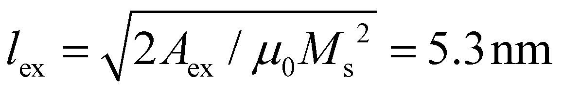 . The geometry is meshed using NetGen43 with a minimum node spacing of 2 nm and a maximum spacing of 3.5 nm. A wire length of 1 μm was used in all micromagnetic simulations. The central 300 nm segment is initialized with a random magnetization, and the magnetization in the lateral segments are fixed pointing towards or away from the central randomized region, forming head-to-head (H–H) or tail-to-tail (T–T) DWs upon relaxation, respectively. The relaxation simulations have been repeated 20 times, with different random seeds, for both H–H and T–T configurations. The simulations are stopped when |dm/dt| < 1.745 × 10⁻² deg s−1, where convergence is satisfied when the largest value of |dm/dt| drops below this value.
Results and discussion
An overview of the fabrication process is shown schematically in Fig. 1. Resist is drop-cast onto a glass substrate (Fig. 1a) into which a 3D geometry is exposed (Fig. 1b). Development washes away unexposed regions yielding a freestanding 3D polymer (Fig. 1c). Finally, thermal evaporation is used to coat Permalloy (Ni81Fe19) upon the 3D nanowires (Fig. 1d). By harnessing a shorter λ = 405 nm laser to polymerize the resist, lateral features below 100 nm is possible.39 | ||
| Fig. 1 Overview of the fabrication process. (a) Negative-tone photoresist (yellow) drop-cast on glass substrate (blue). (b) Exposure of wavelength λ = 405 nm laser. (c) Unexposed resist is removed through solvent development and polymer (purple) nanowires remain. (d) Thermal evaporation of Permalloy (Ni81Fe19, grey) is used to coat the polymer nanowires. | ||
The resulting structures are 3D ferromagnetic sinusoidal nanowires (SNWs) with both longitudinal and cross-sectional curvature. The longitudinal curvature of the SNWs is controlled through the spatial wavelength L of the sinusoidal exposure trajectory with values L = 1 μm, 2 μm and 5 μm, whilst its amplitude is fixed at A = 500 nm, as sketched in Fig. 2(a). The mean lateral feature sizes wavg of the fabricated SNWs for the three spatial periods were measured using SEM and are plotted in Fig. 2(b) as a function of inverse scanning velocity 1/v which is proportional to the effective exposure dose. The data points correspond to the measurements and the solid lines to a fitted profile of the form  (modified from ref. 44 assuming a Gaussian dose shape), where v is the scanning velocity, vth is the threshold velocity and b is the width of the dose shape (see ESI†). We find that SNWs with feature sizes as low as 70 nm can be readily fabricated. The fits generally yield threshold velocities and voxel widths which agree within the estimated measurement error (see ESI†). Example SEM images of SNWs with nominal lateral widths of 80 nm are shown in Fig. 2(c) for L = 1 μm, Fig. 2(d) for L = 2 μm and Fig. 2(e) for L = 5 μm. In addition to SEM, the lateral features of SNWs with spatial period L = 5 μm were further measured using quantitative differential interference contrast (qDIC) microscopy prior to thermal evaporation (see ESI†).45–48 This provides a direct measurement of the polymer cross-sectional area, and by assuming the cross-section is an ellipse, we can determine the axial length of the polymer and thus the aspect ratio of the voxel volume (see ESI Fig. S1†). Analysis of the qDIC images (see ESI†) yields a lateral width w = 100 nm and axial length l = 725 nm. The measured qDIC and SEM widths agree to within 20% (see ESI†).
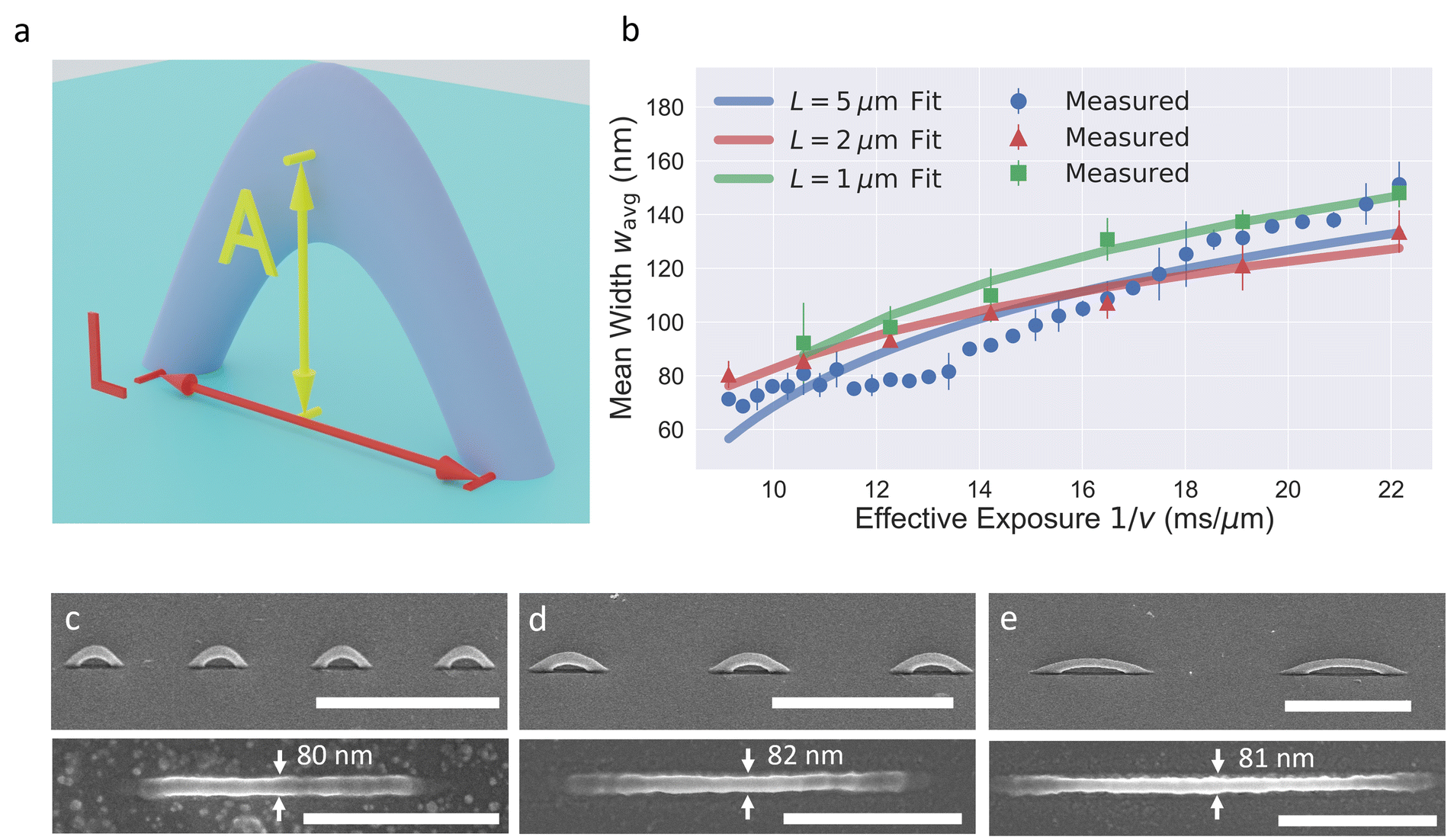 | ||
| Fig. 2 Physical characterization of 3D magnetic nanowires. (a) Schematic of a SNW with spatial period L (red) and amplitude A (yellow). (b) Average SNW width wavg for L = 5 μm (blue circles), L = 2 μm (red triangles) and L = 1 μm (green squares) measured using SEM. Solid lines show fits to expected dependence. The orange cross shows the width as determined by qDIC before evaporation. (c) L = 1 μm, (d) L = 2 μm and (e) L = 5 μm SEM images taken from 45° (top panel), where wires are fabricated well above the polymerization threshold, and top-down (bottom-panel) views, where wires are fabricated close to polymerization threshold. Variations in substrate tilt lead to wires with smaller experimental length. Scale bars are 5 μm and 1 μm in top and bottom panels, respectively. | ||
Magnetic nanowires fabricated using the combination of two-photon DLW and thermal evaporation are known to result in a crescent-shaped cross-section31 where similar structures have recently been studied numerically, elucidating high-frequency spin-wave dispersion relations.49 However, the DW textures that these systems may yield have not yet been studied in detail. Finite-element micromagnetic simulations (see ESI†) were used to determine the spin texture of domain walls that one might expect in the experimental SNWs studied in this work. The SNWs host two distinct geometric curvatures: the longitudinal curvature κl, defined by the spatial period of the sinusoid trajectory, Fig. 2(a); and the cross-sectional curvature κc, defined by the shape of the voxel, Fig. 3(a)–(c). To ensure an accurate geometric mesh in the simulations, the focused laser point spread function (PSF) was calculated (see ESI, Fig. S2†) and is shown in Fig. 3(a), yielding a voxel width lxy = 66 nm, and voxel height lz = 164 nm, and an aspect ratio β = 2.48 at 80% total squared intensity.
 | ||
| Fig. 3 Harnessing the point spread function curvature to realise novel domain walls. (a) Voxel of a circularly polarized λ = 405 nm laser focused through a NA = 1.4, 63× oil immersion (n = 1.518) objective lens. The innermost (dark blue) isosurface corresponds to a polymerization threshold of 80% the total I2. The voxel width lxy = 66 nm, and voxel height lz = 164 nm, and aspect ratio β = 2.48. (b) Illustration of a voxel (bright blue) scanning uniformly in a lateral direction creating a polymer (purple) wire (top), and 40 nm Ni81Fe19 (grey) evaporation on top of this wire (bottom). (c) Cross-sectional view of the nanowire mesh, with outer major and minor radii sa and ra (blue dashed arrows) and inner major and minor radii sb and rb (red solid arrows). (d) Coupled-transverse domain wall (CTW) top-down (top panel), (e and f) side-view and (g) 3D view with inset showing cross-section. Color scheme corresponds to mz component of the reduced magnetization vector m. | ||
The Permalloy deposition process was then simulated by linear extrusion of the calculated PSF along the wire, as shown schematically in Fig. 3(b). Previous work has shown that such thermal evaporation of NiFe normal to the substrate yields a crescent-shaped cross-section as depicted in Fig. 3(b) lower-panel. The geometry of the magnetic nanowire cross-section is defined as the difference of two ellipses, a and b, with major radii sa = 120 nm and sb = 80 nm, and minor radii ra = 42 nm and rb = 40 nm, Fig. 3(c). The peak cross-sectional curvature value κc = 18.8 μm−1 which yields κc ≈ 8κl for the L = 1 μm case. The peak longitudinal curvatures in the experimental systems are κl = 0.10 μm−1 for L = 5 μm; κl = 0.62 μm−1 for L = 2 μm; and κl = 2.47 μm−1 for L = 1 μm. Therefore, one would expect that any curvature-induced perturbation of the DW textures would arise from κc rather than κl, and thus we model here straight segments of wire with purely cross-sectional curvature. Fig. 3(d–g) shows the ground state domain wall configuration comprising two transverse-like textures with aligned in-plane components, to yield a continuous magnetization transition across the wire apex (Fig. 3d) without a topological defect. The two sides of the DW are then found to have opposing mz as shown in Fig. 3(e and f), minimizing the magnetostatic energy. A 3D representation of the wall shows a canting of magnetization into the z direction due to the curvature-induced DMI. We now briefly consider the higher energy DWs obtained in simulations, which we note would not be likely observable in experimental conditions unless subject to necessary external perturbations. ESI, Fig. S3† shows the stabilization of an anti-vortex wall (AVW) which features two transverse-like textures but both with −mz component. Since the magnetization on either side of the curvature peak are anti-aligned (Fig. S3a†), together with the opposing magnetization along the wire axis, this provides the boundary condition for an anti-vortex (topological charge, n = −1) at the curvature peak. Defects of total topological charge n = 1/2 are located on each opposing wire edge. We note that such anti-vortex walls have not been observed in conventional planar nanowires. The walls are likely enabled by the 3D curved geometry allowing both sides of the nanowire to have the same mz component, whilst being spatially separated (reducing the magnetostatic energy), the geometry also yields an effective DMI strongest at peak curvature, stabilizing the central portion of the anti-vortex which is aligned in the z-direction. Compared with the ground state CTW, the AVW has approximately 2% larger total energy, mainly due to the texture surrounding the anti-vortex and the out-of-plane component at the anti-vortex core. Even more complex domain wall types appearing at higher energy (see ESI, Table 1†) are shown in ESI Fig. S4 and S5.† Overall, the micromagnetic simulations demonstrate a range of novel domain wall spin textures, distinct from previously reported textures in curved NiFe caps,50 which occur due to the 3D wire geometry with strong cross-sectional curvature.
With a good understanding of the possible domain walls, we proceeded to carry out imaging experiments aimed at injection and subsequent pinning of DWs in the 3D nanowire, using magnetic force microscopy (MFM) under externally applied magnetic fields (see ESI†). We note that whilst MFM does not have the resolution to resolve the fine structure of the domain walls, it provides a means to probe the energy landscape of the wire by observation of pinning and depinning events. An example 5 μm × 5 μm AFM image of a SNW with period L = 5 μm is shown in Fig. 4(a), and a 3D representation of the same SNW is given in Fig. 4(b). The SNWs studied have a width around 80 nm and are fabricated close to the polymerization threshold, yielding a strong dependence of voxel size on exposure dose. This enhances the surface and edge roughness due to the temporal fluctuations in the laser power during writing and allows pinning of walls at specific wire locations. The fast scan axis in Fig. 4(a) is aligned with the long axis of the SNW, the x-axis. The slow scan axis (i.e. motion of the tip along the y-axis) is disabled once the image acquisition is shown to be scanning along the SNW, as indicated by the red dashed line in Fig. 4(a). By scanning along this direction, the stray field from the tip Htip, when superposed with an external in-plane field Hext, allows the DW to explore its local energy landscape and pinning events are observed directly. In Fig. 4(c and d), a fixed field μ0Hext = 0.2 mT is applied along the positive x-direction for the entire image capture and the image is captured bottom-to-top. It is interesting to note contrast observed at the wire edges, where an abrupt change in topography takes place and the wire interfaces with the sheet film. Experiments have demonstrated that this contrast is magnetic in origin, due to contrast inversion at high fields (ESI Fig. S6†). We note that it is difficult to deduce the exact spin texture at the wire/sheet film interfaces, but show possible configurations in ESI Fig. S7.†
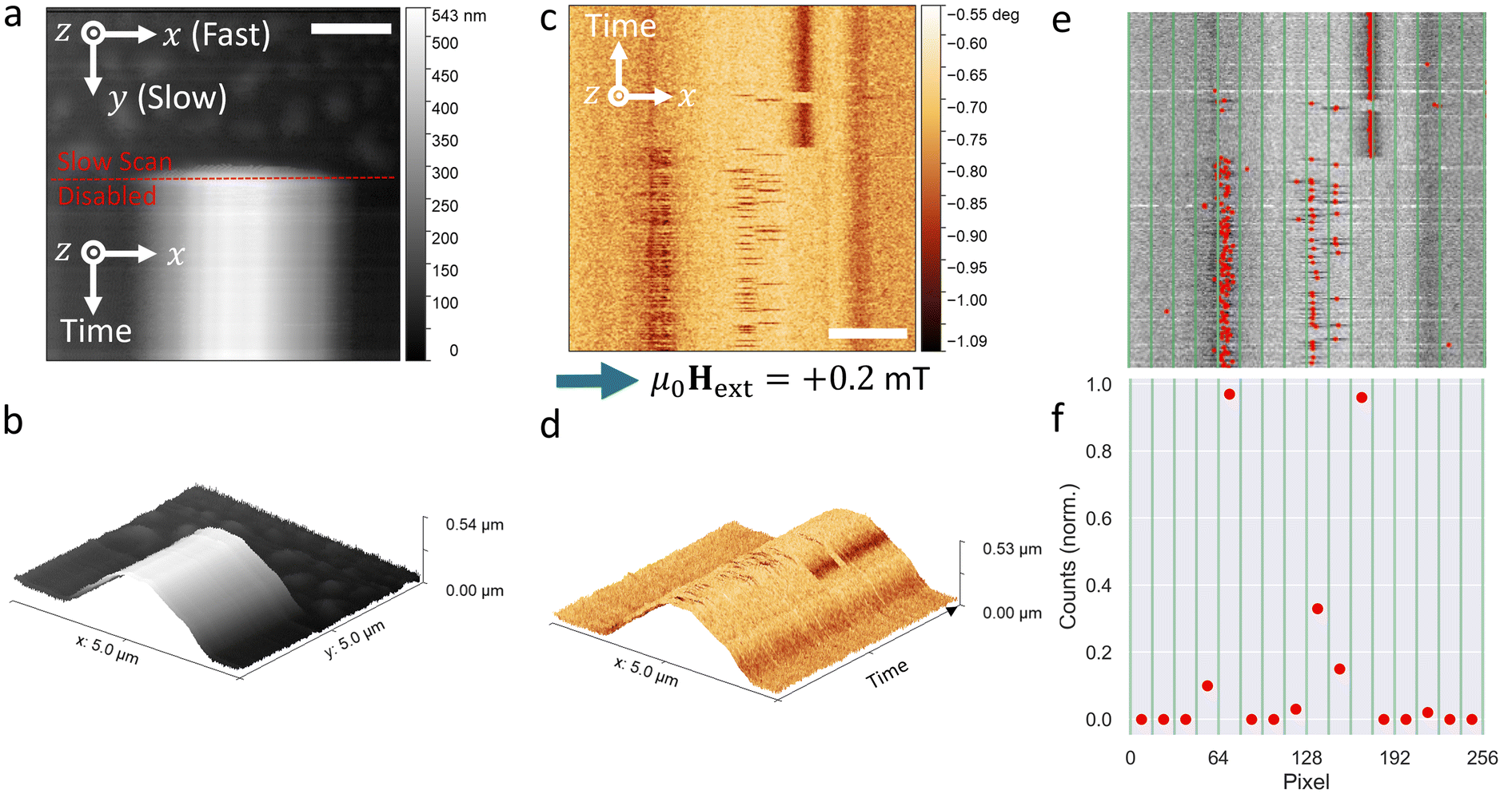 | ||
| Fig. 4 Magnetic force microscopy procedure. (a) Example AFM image of L = 5 μm SNW, with fast and slow scanning axes indicated by white arrows. The slow scan axis is paused when scanning along the SNW. (b) 3D view of the AFM image. (c) MFM image with fixed positive external field μ0Hext = +0.2 mT (blue arrow) applied along the +x-direction. Image capture is bottom-to-top. A head-to-head DW is stochastically pinned and de-pinned along the wire during the scan. (d) 3D view of the MFM image in (c), illustrating the positions of the domain wall. (e) Fitted Gaussian peak positions (red dots) corresponding to domain wall positions along the SNW. (f) Normalised counts of domain wall positions as function of pixel index of (e), green lines correspond to a 16-pixel binning window. Scale bars in all images are 1 μm. | ||
The data in Fig. 4 show stochastic pinning and de-pinning of DWs within central region of the SNW. Schematics in ESI Fig. S7† illustrate the overall domain configuration. To gain insight into pinning positions along the SNWs, multiple MFM images are taken for different fixed fields, and the DW positions are identified on a line-by-line basis (see ESI†), as shown in Fig. 4(e) where the red dots correspond to the DW positions. Fig. 4(f) illustrates the normalized counts of pinning events observed in Fig. 4(e). To build a statistical representation of the pinning potential across the wire, the observed DW positions are collated into histograms by binning over a 16-pixel range. We note that this analysis was not meaningful for L = 1 μm SNWs since the observed DW contrast was exclusively located at the edges of the SNW – a hypothesis for this behavior is discussed later in the manuscript.
SEM images taken at a 45° viewing angle for L = 5 μm and L = 2 μm are shown in Fig. 5(a and b), respectively, with corresponding DW position heatmaps in Fig. 5(c and d). For both wires, one can see that even for a fixed value of μ0Hext the DW positions can fluctuate between different pinning sites along the SNW axis, as is especially the case for μ0Hext = +0.2 mT for L = 5 μm (Fig. 5c), and μ0Hext = +0.5 mT for L = 2 μm (Fig. 5d). This indicates that the DW pinning and motion along the SNWs possess some degree of stochasticity, likely driven by the stray field from the MFM tip during the scans, though this is somewhat reduced where μ0Hext = 0 mT in both the L = 5 μm and L = 2 μm cases. There are also clear and distinct bands of DW pinning over large ranges in the −μ0Hext for the L = 5 μm case at x = 0.78 μm, x = 2.34 μm and x = 3.28 μm, which indicates that there is a significant pinning potential that must be overcome in these regions. Such bands of DW pinning are not as significant in the L = 2 μm case in either ±μ0Hext but there are bands of weaker pinning at x = 0.12 μm and x = 0.88 μm in the +μ0Hext panel.
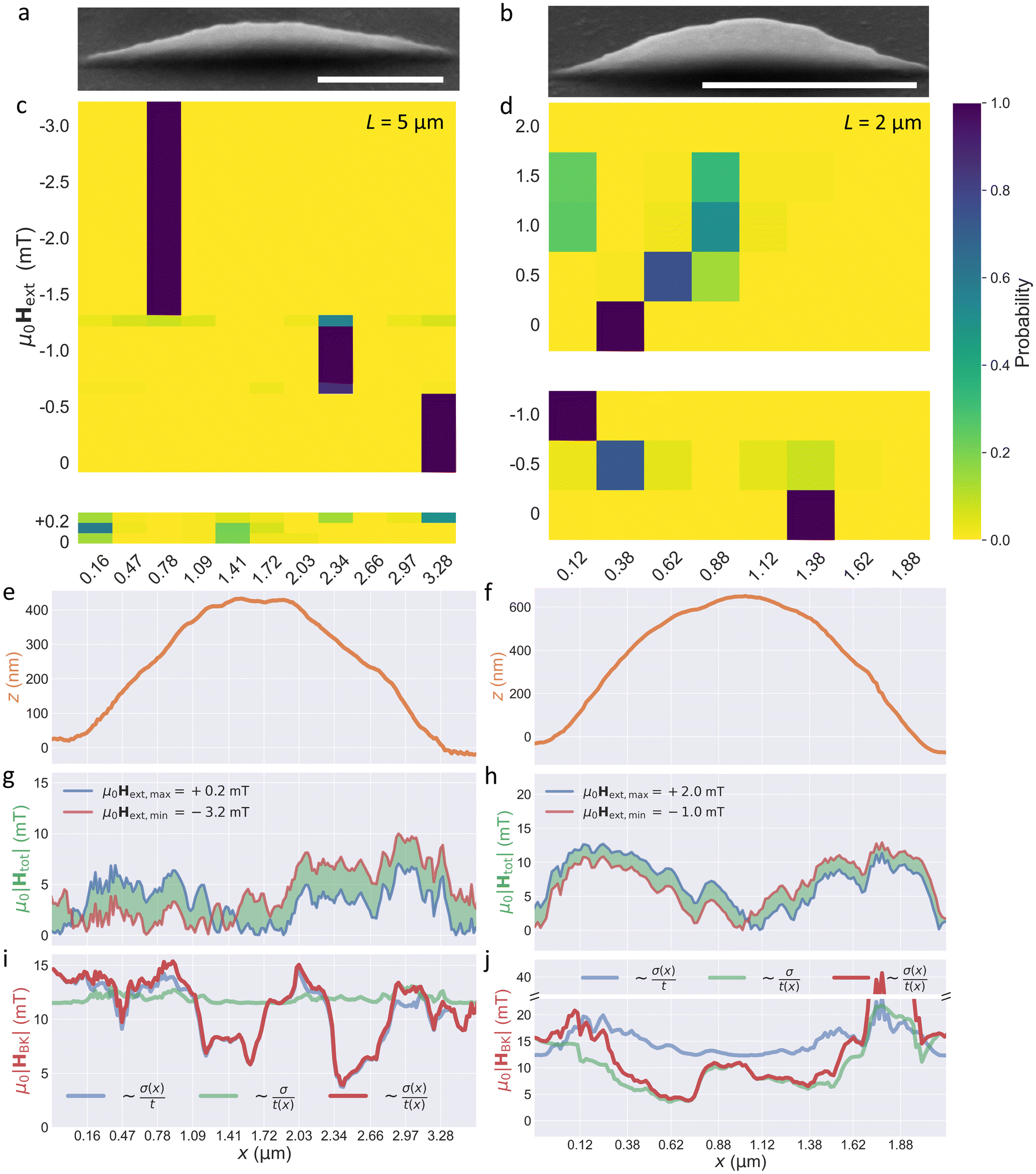 | ||
| Fig. 5 Probing the energy landscape of 3D magnetic nanowire. (a and b) SEM images taken at 45° viewing angle of L = 5 μm and L = 2 μm SNWs, respectively, scale bars 1 μm. (c and d) DW pinning position probability maps as function of longitudinal position x along the SNW and the applied field μ0Hext. (e and f) AFM line profiles used in the determination of the SNW roughness. (g and h) Total field magnitude μ0|Htot| due to external field μ0Hext and field from MFM tip μ0Htip projected along the SNW tangent. (i and j) Becker–Kondorski depinning field magnitude μ0|HBK| with varying roughness constant thickness (blue line), constant roughness varying thickness (green line), and varying roughness varying thickness (red line). | ||
The peaks of the SNWs are approximately 1.72 μm for L = 5 μm, and 1.00 μm for L = 2 μm. For L = 5 μm there is no significant pinning at the apex, with strong bands of pinning occurring in regions along the ascending regions of the SNW. Weak pinning is observed at the apex of the L = 2 μm case, though these pinning events mainly fall into the x = 0.88 μm bin rather than the x = 1.22 μm, likely driven by the positive field direction which propagates the DW in the +x-direction, though the reverse situation for a negative field does not result in stronger pinning in the x = 1.22 μm bin. The lack of, or weakly observed, pinning at the regions of maximal longitudinal curvature contrasts with similar experimental and theoretical studies on curvature induced DW pinning in ferromagnetic parabolic stripes, where DW pinning was observed at local curvature maxima.51,52 Recent theoretical work on similar parabolic stripes with tailored cross-sectional thicknesses has illustrated that spatially varying cross-sections can provide additional sources of geometry-induced DMI and anisotropy,53 and can lead to DW pinning regions adjacent to the typical pinning sites at the local curvature maxima where the cross-section is at a minimum. In the present case, the spatially varying cross-section, Fig. 3(c), is not believed to induce the pinning observed in Fig. 5(b) and (g) as the cross-section is approximately constant along the SNW period, so we consider other reasons for the observed pinning landscape.
DW pinning typically arises due to the presence of material defects which can include dislocations, impurities, grain boundaries and other inhomogeneities; polycrystallinity and surface roughness.54 It is well-known that thermally evaporated Ni81Fe19 in identical systems used in the set-up at present produce highly pure deposits with ratios of Ni to Fe being 4.26,31,33 with small grains of less than a few nm, has a well-defined face-centered cubic crystal structure in films thinner than 60 nm55 and has negligible magnetocrystalline anisotropy. We therefore consider SNW surface roughness induced pinning, with clear roughness features observable in the SEM images in Fig. 5(a and b), as the potential source of the observed behavior in Fig. 5(c and d). AFM line profiles of the L = 5 μm and L = 2 μm SNWs are shown in Fig. 5(e and f), respectively. We first consider the total field Htot experienced by decomposing the external field Hext and the field from the tip Htip along the local SNW tangent (see ESI†), where the absolute values μ0|Htot| are shown in Fig. 5(g and h) for L = 5 μm and L = 2 μm, respectively. The blue curves correspond to the maximal external field μ0Hext,max, and the red curves to the minimum external field μ0Hext,min, with the green shaded regions corresponding to the intermediate values investigated in the partial hysteresis loops. Both Fig. 5(g) and (h) reveal the rather strong field component provided by the tip (5–10 mT), which facilitates DW movement in regions where the nanowire tangent has an out-of-plane component.
Following the work of Schöbitz et al.54 and Bruno,56 we derive an expression for the depinning field due to roughness, arising from magnetostatic contributions to anisotropy, using a Becker–Kondorski model, within a planar nanowire approximation and ignoring any magnetostatic interaction with the surrounding sheet film.57 The result of this analysis (see ESI†) predicts a depinning field 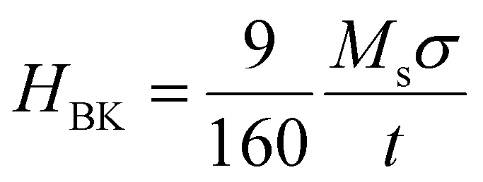 , where σ is the surface root-mean-square (RMS) roughness, and t is the thickness of the Ni81Fe19 layer. We therefore expect the depinning field to scale with roughness and inversely with thickness and consider both in our analysis. Simple geometric considerations yield a local thickness t′ = t
![[thin space (1/6-em)]](https://www.rsc.org/images/entities/char_2009.gif) cosθ where θ is the angle between nanowire tangent and substrate and t is the thickness deposited on a flat region. The local RMS roughness for L = 5 μm with value σ = 7.6 nm can vary up to 60% over the nanowire length, and for L = 2 μm with value σ = 8.1 nm which can vary up to 75% over the nanowire length, whilst local variations in wire thickness are up to 15% for L = 5 μm and up to 50% for L = 2 μm. It is therefore anticipated that the sites of largest depinning field will arise from the combined effects of reduced thickness and increased roughness, with roughness dominating for larger L, and thickness variations dominating for smaller L (see ESI, Fig. S6†). The depinning field μ0|HBK| for both geometries is calculated directly using the AFM topography within the Becker–Kondorski framework and is shown in Fig. 5(i and j) for the L = 5 μm and L = 2 μm SNWs, respectively. Three cases are plotted, varying roughness and constant thickness; constant roughness (equal to the RMS roughness for each nanowire) and varying thickness (green); and the combination of varying roughness and thickness (red). It can be seen that the depinning fields for both wires are the same order of magnitude as the applied fields, suggesting pinning events are likely to be observed. Two regimes of pinning can be identified in both nanowires, with higher depinning fields observed in regions of high slope due to the reduced thickness, and lower depinning fields observed at flatter regions near the center, driven by the local roughness, largely matching the general pinning trend seen in Fig. 5(c and d). Differences in the experimental pinning probabilities between the two nanowires can be understood by considering the field component tangential to the wire direction. The L = 2 μm nanowire, though possessing a higher calculated depinning field in regions of higher slope, also has a larger out-of-plane field component along the wire, making strong pinning less likely and instead the DW hops between pinning sites in sloped regions. In contrast, the L = 5 μm nanowire is seen to have well-defined bands of pinning with probability close to 1. Here, the calculated depinning field is of similar magnitude to that of the L = 2 μm but the component of the field along the nanowire is reduced, favouring pinning of DWs at a single site. For L = 1 μm (see ESI, Fig. S8†) the depinning fields were found to be μ0|HBK| = 90 mT at one edge, whilst the total field along the SNW tangent never exceeded μ0|Htot| = 20 mT, lending insight into the lack of stochastic DW pinning.
cosθ where θ is the angle between nanowire tangent and substrate and t is the thickness deposited on a flat region. The local RMS roughness for L = 5 μm with value σ = 7.6 nm can vary up to 60% over the nanowire length, and for L = 2 μm with value σ = 8.1 nm which can vary up to 75% over the nanowire length, whilst local variations in wire thickness are up to 15% for L = 5 μm and up to 50% for L = 2 μm. It is therefore anticipated that the sites of largest depinning field will arise from the combined effects of reduced thickness and increased roughness, with roughness dominating for larger L, and thickness variations dominating for smaller L (see ESI, Fig. S6†). The depinning field μ0|HBK| for both geometries is calculated directly using the AFM topography within the Becker–Kondorski framework and is shown in Fig. 5(i and j) for the L = 5 μm and L = 2 μm SNWs, respectively. Three cases are plotted, varying roughness and constant thickness; constant roughness (equal to the RMS roughness for each nanowire) and varying thickness (green); and the combination of varying roughness and thickness (red). It can be seen that the depinning fields for both wires are the same order of magnitude as the applied fields, suggesting pinning events are likely to be observed. Two regimes of pinning can be identified in both nanowires, with higher depinning fields observed in regions of high slope due to the reduced thickness, and lower depinning fields observed at flatter regions near the center, driven by the local roughness, largely matching the general pinning trend seen in Fig. 5(c and d). Differences in the experimental pinning probabilities between the two nanowires can be understood by considering the field component tangential to the wire direction. The L = 2 μm nanowire, though possessing a higher calculated depinning field in regions of higher slope, also has a larger out-of-plane field component along the wire, making strong pinning less likely and instead the DW hops between pinning sites in sloped regions. In contrast, the L = 5 μm nanowire is seen to have well-defined bands of pinning with probability close to 1. Here, the calculated depinning field is of similar magnitude to that of the L = 2 μm but the component of the field along the nanowire is reduced, favouring pinning of DWs at a single site. For L = 1 μm (see ESI, Fig. S8†) the depinning fields were found to be μ0|HBK| = 90 mT at one edge, whilst the total field along the SNW tangent never exceeded μ0|Htot| = 20 mT, lending insight into the lack of stochastic DW pinning.
Overall, the model provides a spatial variation of depinning field that is generally consistent with the experimental data, when also considering the total magnetic field at different points on the wires. We note that some discrepancies between the calculated pinning and experimental data are observed. Most notable is at x = 1.88 μm, for the L = 2 μm wire where |Htot| ≪ |HBK|, and yet no pinning behavior is observed. We also note that in some instances, pinning appears to be preferentially occurring on one side of the nanowire.
Such observations could be related to the following three points. Firstly, the total field μ0|Htot| is estimated assuming a perfectly aligned dipole perpendicular to the sample surface. Slight deviations due to substrate tilt or any imperfections in tip fabrication will yield perturbations in the field experienced. We note that the intricate field distribution around a realistic pyramidal tip, may yield a stray field pinning the magnetization beyond the apex and reducing the possibility for the wall to move to the other side of the wire. Secondly, the calculated depinning fields are based on a model with planar approximation and this considers neither the non-planar cross-section of the nanowires nor the 3D stray field of the underlying domain walls. Thirdly, we note that the forward and backward scanning of the tip, when combined with a geometric variation in pinning potential will yield stochasticity in DW movement.
Conclusions
We have presented a novel means to fabricate sub-100 nm 3D ferromagnetic nanowires with cross-sectional and longitudinal curvature using a modified two-photon lithography direct laser writing system. Physical characterization of these 3D nanostructures shows that we can consistently fabricate nanostructures with lateral features below 100 nm, as predicted by the numerically modelled PSF. Finite-element micromagnetic simulations demonstrate that such nanowires with crescent-shaped cross-section are home to several exotic DWs not previously reported in the literature. MFM in externally applied magnetic fields has been used to study nucleation and pinning of DWs in the nanowires. The observed pinning behavior can be understood within the context of thickness gradients and surface roughness across the nanowire. It is expected that careful tuning of exposure settings and geometric parameters of the fabrication will allow a reduction in surface roughness, whilst a more conformal coating of magnetic material may be achieved by using atomic layer deposition, as demonstrated recently on 3D woodpile structures,58 or using substrate tilt and rotation during conventional deposition. Ultimately, our method can be used to realize 3D magnetic nanostructures of chosen geometry, by design, allowing the study of a wide range of topological spin textures and their time-dependent phenomena.Author contributions
The manuscript was written through contributions of all authors. All authors have given approval to the final version of the manuscript. Conceptualization, S. L. and W. L.; methodology, M. H., A. H., J. A., L. P., I. P., S. L., W. L.; software, M. H. and J. A.; validation, M. H., J. A., L. P., I. P., A. V. D. B.; formal analysis, M. H. and J. A.; investigation, M. H., J. A., L. P., I. P.; resources, S. L. and W. L.; data curation, M. H. and J. A.; writing – original draft preparation, M. H., J. A. and S. L.; writing – review & editing, M. H., J. A., S. L., W. L.; visualization, J. A.; supervision, S. L. and W. L.; project administration, S. L. and W. L.; funding acquisition, S. L. and W. L.Data availability
The data that support the findings of this study are openly available in the Cardiff University data catalog at https://doi.org/10.17035/cardiff.26763172.Conflicts of interest
There are no conflicts to declare.Acknowledgements
This work was funded by the Engineering and Physics Research Council (EPSRC) grant numbers EP/R009147/1 and EP/X012735/1. S. L. also acknowledges funding from the Leverhulme Trust, grant number RPG-2021-139.References
- D. A. Allwood, et al., Magnetic domain-wall logic, Science, 2005, 309(5741), 1688–1692 CrossRef CAS.
- G. Hrkac, J. Dean and D. A. Allwood, Nanowire spintronics for storage class memories and logic, Philos. Trans. R. Soc., A, 2011, 369(1948), 3214–3228 CrossRef CAS.
- S. S. P. Parkin, M. Hayashi and L. Thomas, Magnetic domain-wall racetrack memory, Science, 2008, 320(5873), 190–194 CrossRef CAS.
- S. Parkin and S. H. Yang, Memory on the racetrack, Nat. Nanotechnol., 2015, 10(3), 195–198 CrossRef CAS.
- K. Yue, et al., A brain-plausible neuromorphic on-the-fly learning system implemented with magnetic domain wall analog memristors, Sci. Adv., 2019, 5(4), eaau8170 CrossRef.
- J. C. Gartside, et al., Reconfigurable training and reservoir computing in an artificial spin-vortex ice via spin-wave fingerprinting, Nat. Nanotechnol., 2022, 17(5), 460–469 CrossRef CAS.
- A. Mukhtar, et al., Magnetic nanowires in biomedical applications, Nanotechnology, 2020, 31(43), 433001 CrossRef CAS.
- C. Donnelly, et al., Three-dimensional magnetization structures revealed with X-ray vector nanotomography, Nature, 2017, 547(7663), 328–331 CrossRef CAS.
- R. Hertel, Ultrafast domain wall dynamics in magnetic nanotubes and nanowires, J. Phys.: Condens. Matter, 2016, 28, 483002 CrossRef CAS.
- S. Da Col, et al., Observation of Bloch-point domain walls in cylindrical magnetic nanowires, Phys. Rev. B: Condens. Matter Mater. Phys., 2014, 89, 180405 CrossRef.
- Y. P. Ivanov, et al., Modulated Magnetic Nanowires for Controlling Domain Wall Motion: Toward 3D Magnetic Memories, ACS Nano, 2016, 10(5), 5326–5332 CrossRef CAS.
- A. Wartelle, et al., Bloch-point-mediated topological transformations of magnetic domain walls in cylindrical nanowires, Phys. Rev. B, 2019, 99(2), 024433 CrossRef CAS.
- Y. P. Ivanov, et al., Single crystalline cylindrical nanowires – toward dense 3D arrays of magnetic vortices, Sci. Rep., 2016, 6, 23844 CrossRef CAS.
- J. Fernandez-Roldan, et al., Magnetization pinning in modulated nanowires: from topological protection to the “corkscrew” mechanism, Nanoscale, 2018, 10(13), 5923–5927 RSC.
- A. Fernández-Pacheco, et al., Three-dimensional nanomagnetism, Nat. Commun., 2017, 8(1), 1–14 CrossRef PubMed.
- D. Sheka, V. Kravchuk and Y. Gaididei, Curvature effects in statics and dynamics of low dimensional magnets, J. Phys. A: Math. Theor., 2015, 48(12), 125202 CrossRef.
- Y. Gaididei, V. P. Kravchuk and D. D. Sheka, Curvature Effects in Thin Magnetic Shells, Phys. Rev. Lett., 2014, 112(25), 257203 CrossRef PubMed.
- R. Streubel, et al., Magnetism in curved geometries, J. Phys. D: Appl. Phys., 2016, 49(36), 363001 CrossRef.
- K. Yershov, et al., Curvature-induced domain wall pinning, Phys. Rev. B: Condens. Matter Mater. Phys., 2015, 92(10), 104412 CrossRef.
- O. Volkov, et al., Experimental Observation of Exchange-Driven Chiral Effects in Curvilinear Magnetism, Phys. Rev. Lett., 2019, 123(7), 077201 CrossRef CAS.
- K. Gu, et al., Three-dimensional racetrack memory devices designed from freestanding magnetic heterostructures, Nat. Nanotechnol., 2022, 17, 1065–1071 CrossRef CAS.
- M. Huth, et al., Focused electron beam induced deposition: A perspective, Beilstein J. Nanotechnol., 2012, 3, 597–619 CrossRef CAS.
- D. Sanz-Hernandez, et al., Fabrication, Detection, and Operation of a Three-Dimensional Nanomagnetic Conduit, ACS Nano, 2017, 11(11), 11066–11073 CrossRef CAS.
- L. Skoric, et al., Layer-by-layer growth of complex-shaped three-dimensional nanostructures with focused electron beams, Nano Lett., 2019, 20(1), 184–191 CrossRef PubMed.
- C. Donnelly, et al., Complex free-space magnetic field textures induced by three-dimensional magnetic nanostructures, Nat. Nanotechnol., 2022, 17(2), 136–142 CrossRef CAS PubMed.
- D. Sanz-Hernandez, et al., Artificial Double-Helix for Geometrical Control of Magnetic Chirality, ACS Nano, 2020, 14(7), 8084–8092 CrossRef CAS.
- A. Fernandez-Pacheco, et al., Three dimensional magnetic nanowires grown by focused electron-beam induced deposition, Sci. Rep., 2013, 3, 1492 CrossRef.
- A. Fernandez-Pacheco, et al., Writing 3D Nanomagnets Using Focused Electron Beams, Materials, 2020, 13(17), 3774 CrossRef CAS.
- M. Hunt, et al., Harnessing multi-photon absorption to produce three-dimensional magnetic structures at the nanoscale, Materials, 2020, 13(3), 761 CrossRef CAS PubMed.
- J. Askey, et al., Use of Two-Photon Lithography with a Negative Resist and Processing to Realise Cylindrical Magnetic Nanowires, Nanomaterials, 2020, 10(3), 429 CrossRef CAS PubMed.
- A. May, et al., Realisation of a frustrated 3D magnetic nanowire lattice, Commun. Phys., 2019, 2(1), 1–9 CrossRef.
- A. May, et al., Magnetic charge propagation upon a 3D artificial spin-ice, Nat. Commun., 2021, 12(1), 3217 CrossRef CAS PubMed.
- A. van den Berg, et al., Combining two-photon lithography with laser ablation of sacrificial layers: A route to isolated 3D magnetic nanostructures, Nano Res., 2023, 16(1), 1441–1447 CrossRef CAS.
- G. Williams, et al., Two photon lithography for 3D Magnetic Nanostructure Fabrication, Nano Res., 2018, 11, 845–854 CrossRef.
- S. Sahoo, et al., Observation of Coherent Spin Waves in a Three-Dimensional Artificial Spin Ice Structure, Nano Lett., 2021, 21(11), 4629–4635 CrossRef CAS.
- M. Saccone, et al., Exploring the phase diagram of 3D artificial spin-ice, Commun. Phys., 2023, 6(1), 217 CrossRef CAS.
- J. Fischer and M. Wegener, Three-dimensional optical laser lithography beyond the diffraction limit, Laser Photonics Rev., 2013, 7(1), 22–44 CrossRef CAS.
- P. Pip, et al., X-ray imaging of the magnetic configuration of a three-dimensional artificial spin ice building block, APL Mater., 2022, 10(10), 101101 CrossRef CAS.
- P. Mueller, M. Thiel and M. Wegener, 3D direct laser writing using a 405 nm diode laser, Opt. Lett., 2014, 39(24), 6847–6850 CrossRef.
- D. Nečas and P. Klapetek, Gwyddion: an open-source software for SPM data analysi, Cent. Eur. J. Phys., 2012, 10, 181–188 Search PubMed.
- T. Fischbacher, et al., A systematic approach to multiphysics extensions of finite-element-based micromagnetic simulations: Nmag, IEEE Trans. Magn., 2007, 43(6), 2896–2898 Search PubMed.
- S. Jamet, et al., Head-to-head domain walls in one-dimensional nanostructures: An extended phase diagram ranging from strips to cylindrical wires, in Magnetic Nano- and Microwires, ed. M. Vazquez, Woodhead Publishing, 2015, pp. 783–811 Search PubMed.
- J. Schöberl, NETGEN An advancing front 2D/3D-mesh generator based on abstract rules, Comput. Visualization Sci., 1997, 1, 41–52 CrossRef.
- H.-B. Sun, et al., Scaling laws of voxels in two-photon photopolymerization nanofabrication, Appl. Phys. Lett., 2003, 83(6), 1104–1106 CrossRef CAS.
- I. Pope, et al., Coherent anti-Stokes Raman scattering microscopy of single nanodiamonds, Nat. Nanotechnol., 2014, 9(11), 940–946 CrossRef CAS PubMed.
- D. Regan, et al., Measuring sub-nanometre thickness changes during phase transitions of supported lipid bilayers with quantitative differential interference contrast microscopy, in SPIE BiOS, Proc. SPIE, San Francisco, USA, 2019.
- D. Regan, et al., Lipid Bilayer Thickness Measured by Quantitative DIC Reveals Phase Transitions and Effects of Substrate Hydrophilicity, Langmuir, 2019, 35(43), 13805–13814 CrossRef CAS PubMed.
- C. I. McPhee, et al., Measuring the Lamellarity of Giant Lipid Vesicles with Differential Interference Contrast Microscopy, Biophys. J., 2013, 105, 1414–1420 CrossRef CAS PubMed.
- M. Gołębiewski, et al., Spin-Wave Spectral Analysis in Crescent-Shaped Ferromagnetic Nanorods, Phys. Rev. Appl., 2023, 19(6), 064045 CrossRef.
- R. Streubel, et al., Magnetically capped roll-up nanomembranes, Nano Lett., 2012, 12, 3961–3966 CrossRef CAS.
- O. Volkov, et al., Experimental Observation of Exchange-Driven Chiral Effects in Curvilinear Magnetism, Phys. Rev. Lett., 2019, 123, 077201 CrossRef CAS.
- D. D. Sheka, et al., Fundamentals of Curvilinear Ferromagnetism: Statics and Dynamics of Geometrically Curved Wires and Narrow Ribbons, Small, 2022, 18(12), 2105219 CrossRef CAS.
- K. V. Yershov and D. D. Sheka, Control of magnetic response in curved stripes by tailoring the cross-section, Phys. Rev. B, 2023, 107, 104412 CrossRef.
- M. Schöbitz, et al., A Material View on Extrinsic Magnetic Domain Wall Pinning in Cylindrical CoNi Nanowires, J. Phys. Chem. C, 2023, 127(5), 2387–2397 CrossRef.
- S. Lamrani, et al., Microstructure investigation and magnetic study of Permalloy thin films grown by thermal evaporation, Eur. J. Appl. Phys., 2016, 74(3), 30302 CrossRef.
- P. Bruno, Dipolar magnetic surface anisotropy in ferromagnetic thin films with interfacial roughness, J. Appl. Phys., 1988, 64(6), 3153–3156 CrossRef.
- R. Skomski, Simple Models of Magnetism, Oxford University Press, 2008 Search PubMed.
- H. Guo, et al., Realization and Control of Bulk and Surface Modes in 3D Nanomagnonic Networks by Additive Manufacturing of Ferromagnets, Adv. Mater., 2023, 35(39), 2303292 CrossRef CAS.
Footnotes |
| † Electronic supplementary information (ESI) available. See DOI: https://doi.org/10.1039/d4nr02020k |
| ‡ These authors contributed equally. |
| § Present address: Huntleigh Healthcare Ltd, Cardiff, UK. |
| ¶ Present address: VitreaLab GmbH, Vienna, Austria. |
| || Present address: Taibah University – Faculty of Science and Arts, Janada Bin Umayyah Road, Medina 42353, Kingdom of Saudi Arabia. |
| This journal is © The Royal Society of Chemistry 2024 |