
 Open Access Article
 This Open Access Article is licensed under a Creative Commons Attribution-Non Commercial 3.0 Unported Licence
Abrasive-free chemical-mechanical planarization (CMP) of gold for thin film nano-patterning†
Raphael
Gherman
 *ab,
Guillaume
Beaudin
ab,
Romain
Stricher
ab,
Jean-François
Bryche
ab,
Pierre
Levesque
c,
François
Fillion-Gourdeau
cd,
Steve G.
MacLean
cde,
Dominique
Drouin
ab,
Paul G.
Charette
ab and
Serge
Ecoffey
*ab
*ab,
Guillaume
Beaudin
ab,
Romain
Stricher
ab,
Jean-François
Bryche
ab,
Pierre
Levesque
c,
François
Fillion-Gourdeau
cd,
Steve G.
MacLean
cde,
Dominique
Drouin
ab,
Paul G.
Charette
ab and
Serge
Ecoffey
*ab
aInstitut Interdisciplinaire d′Innovation Technologique (3IT), Université de Sherbrooke, 3000 Boulevard de l'université, Sherbrooke, J1K 0A5 Québec, Canada. E-mail: serge.ecoffey@usherbrooke.ca
bLaboratoire Nanotechnologies Nanosystèmes (LN2)-IRL3463, CNRS, Université de Sherbrooke, Sherbrooke, J1K 0A5 Québec, Canada
cInstitute for Quantum Computing, University of Waterloo, Waterloo, Ontario, Canada N2L 3G1
dInfinite Potential Laboratories, Waterloo, Ontario, Canada N2L 0A9
eUniversité du Québec, INRS-Énergie, Matériaux et Télécommunications, Varennes, Québec, Canada J3X 1S2
First published on 8th August 2024
Abstract
Despite high demand for gold film nanostructuring, patterning gold at the nanoscale still presents considerable challenges for current foundry-compatible processes. Here, we present a method based on abrasive-free chemical mechanical planarization (CMP) to planarize nanostructured gold surfaces with high selectivity against SiO2. The method is efficient in a damascene process and industry-compatible. Investigations into the material removal mechanism explore the effects of CMP parameters and show that the material removal rate is highly tunable with changes in slurry composition. Millimeter-scale arrays of gold nanostructures embedded in SiO2 were fabricated and the planarization dynamics were monitored over time, leading to the identification of distinct planarization phases and their correlation with the material removal mechanism. Finally, plasmonic cavities of gold nanostructure arrays over a gold mirror were fabricated. The cavities exhibited efficient plasmonic resonance in the visible range, aligning well with simulation results.
Introduction
Gold has a combination of unique properties: low electrical resistivity, high optical reflectivity in the visible range, chemical stability, high melting point, high electromigration, biocompatibility, and corrosion resistance.1 As a result, gold is a key material in the fabrication of devices across a wide variety of applications such as electrical interconnects,2–4 electrodes,5 plasmonics,6 ohmic contacts,7 vapour–liquid–solid (VLS) semiconductor nanowires,8 and MEMS.9 In many cases, device fabrication requires micro and nano-patterning, by either dry or wet etching. Dry etching based on reactive ion etching (RIE) suffers from the low volatility of plasma gold etch products at temperatures below 125 °C, causing re-deposition and contamination problems.1 By increasing the temperature, one can simplify the post-process cleaning steps, but this limits the panel of usable patterning resists. Dry etching by ion milling uses an ion plasma to do pure physical etching of the material. This is selectivity-limited as it does not involve any chemical reaction10 and is very slow. Wet etching of gold with nanometer scale feature size for high density and high aspect ratio structures is not possible due to the intrinsic isotropy of this technique. Lift-off, though widely used in research, suffers from low reproducibility, low yield, and incompatibility in general with industrial manufacturing process flows. In response to high demand for gold nano-patterning, various other technologies have been proposed such as nanostencil,11 nanoimprint,12 and laser interference,13 but problems related to reproducibility, and throughput prevent them from being used in high-volume manufacturing.Patterning of metals by chemical-mechanical polishing/planarization (CMP) is heavily used in the semiconductor industry, notably for the fabrication of Cu interconnects. In the case of gold, CMP recipes based on potassium and iodine slurry solutions achieving well controlled material removal rates (MRR) have been published by several academic groups as well as by some industrial manufacturers though most are trade secrets. For example, a University of Windsor group used a slurry solution of fumed silica, I2, KI, citric acid, and trisodium citrate for surface polishing to obtain ultrasmooth Au surfaces equivalent to template stripping.14 NTT Telecommunications Energy Laboratories used a KIO3 based slurry with Al2O3 nanoparticles and H2O2 to fabricate micrometric interconnects on polybenzoxazole (PBO).3 Fujitsu used a Au/SiON damascene process with a slurry composed of KI, I2, H2O2 and silica nanoparticles.2 A University of Notre Dame group investigated a KIO3 alumina based commercial slurry to which they added H2O2 and various surfactants. They also evaluated the effect of the adhesion layer on the damascene structures, mainly micrometric contacts and lines embedded in SiNx.15 Our group published results on CMP-based fabrication of nanowires, nanodots and nanogaps16,17 with a slurry composition similar to the one proposed by Notre Dame. Importantly, these works all reported large numbers of micro and macro defects on the surface.
To address this problem, abrasive-free (or abrasive-less) CMP has been developed for several materials, such as Cu,18 polysilicon,19,20 Ta, TaN21 and Ru.22,23 Indeed, it can be beneficial to use a slurry without an abrasive when the chemical action is strong enough to remove material in combination with the mechanical action of the pad (note that the word “slurry” refers to a solution containing solid particles which is not the case here, nevertheless the term slurry is used below for simplicity and consistency with the CMP literature). As a result, less effort is required to control particle dispersion, filter the slurry, prevent agglomeration, and cleaning. In the case of Cu for example, the abrasive-free CMP mechanism is based on the chemical reaction between the slurry and the native copper oxide to form a complex.24 MRRs of 500 nm min−1 to 2000 nm min−1 have been achieved24 with reductions in oxide loss, recess, erosion, and dishing, resulting in improved repeatability and throughput compared to abrasive CMP.18,25
Our group was the first to propose abrasive-free CMP applied to Au microstructuration4,17 based on the damascene process illustrated in Fig. 1a. The work below presents a comprehensive study of the Au abrasive-free CMP process parameters (slurry dilution and flow rate, platen rotation speed, pad pressure) to better understand how to optimally control the material removal rate and achieve a desired device geometry and surface planarity. The work was conducted in the context of fabricating Au nanostructures embedded in a dielectric (SiO2) by a damascene process. The plasmonics response of a device consisting of an array of Au nanostructures embedded in SiO2 over a gold film are presented to validate the method in a functional application.
 | ||
| Fig. 1 Abrasive-free CMP applied to Au nano-patterning: (a) damascene process and (b) electrochemical reaction for wet etching of Au with iodide/iodine chemistry. | ||
Results and discussion
Unstructured gold thin film CMP and material removal mechanism
CMP uses chemical oxidation by a slurry flow on the sample surface and mechanical force applied by a pad under rotation to remove material and achieve high levels of planarity. However, the noble metal electron configuration of gold makes it highly resistant to oxidation. Consequently, chemical etching of gold requires a potent oxidizer for electron separation and a complexing agent to impede the reassembly of oxidized Au atoms. The iodide/iodine system is one of the most common for gold patterning with wet etching. In the anodic reaction as shown in Fig. 1b, the metal undergoes oxidation giving rise to Au+ ions at the metal-solution interface, subsequently forming a complex with ligands (I−). The cathodic process involves the reduction of the oxidant (I2) at the same interface, consuming the electrons generated by the anodic reaction.7 CMP with gold etchant TFA from Transene CO Inc. (2–4% I2, 40–45% KI, and 51–58% water by weight)26 was performed on 10 × 10 mm2 Si samples coated with a 70 nm evaporated Au film atop a 2 nm Ti adhesion layer. A comprehensive list of CMP parameters can be found in ESI Table S1† and details regarding uncertainty calculations are available in Table S2.†We first investigated the impact of gold etch solution concentration in the slurry, the primary parameter governing the chemical etching rate during the CMP process, where a higher concentration leads to increased reaction kinetics and faster etching. Fig. 2a illustrates the MRR tunability from 30 nm min−1 to 130 nm min−1 by varying the dilution factor from 1/200 to 1/50 (gold etch/water), where the gold removal rate was monitored in real-time. Using pure water only as a slurry, no significant etching of the gold layer was observed, even after extended polishing times. For samples statically immersed in solution at a 1/100 dilution ratio, i.e. without mixing, solution renewal, or mechanical action by the pad, the measured etch rate was 3 nm min−1, a much lower MRR compared to that with CMP at the same gold etch concentration (67 nm min−1). These observations demonstrate that the material removal mechanism in the CMP process, over the measured MRR levels, is the result of both chemical action by the etchant and mechanical interaction with the pad, as explored in more detail below. We observed that for a 1/50 concentrated slurry in the red curve of Fig. 2a, the MRR is very high, and the less than 30 s polishing time of a 70 nm thick Au layer leads to a CMP process that is difficult to control and reproduce.
 | ||
| Fig. 2 (a) Removed Au thickness by abrasive-free CMP as a function of polishing time for various slurry dilution factors; inset: tunability of CMP MRR with dilution factor. (b) Impact of CMP parameters on MRR (platen rotation speed, slurry flow rate, and applied pressure) for 1/100 and 1/200 dilution ratios. | ||
We investigated the impact of platen rotation speed, slurry flow rate, and applied pad pressure, at two different dilution ratios. At a dilution of 1/100, as shown in Fig. 2b (blue curves), increases in rotation speed (2×) and slurry flow (2.5×) both resulted in a ∼1.5× increase in MRR. Indeed, faster platen rotation and increased slurry flow result in more effective transport of fresh gold etchant solution to the sample surface and more efficient removal of etching products. At a dilution of 1/200 (green curves), a similar behavior was observed albeit with smaller MRR increases. Fig. 2b also shows the impact of pad pressure, where increasing the pressure on the samples by three times only led to minor increases in MRR (17% and 7% for 1/100 and 1/200 dilution factors, respectively). This behavior, which does not follow the Preston equation,27 suggests a dominant chemical material removal mechanism. Note that at 1/100 dilution factor, the MRR reaches a maximum at a slurry flow of 75 mL min−1, indicating a saturation of the kinetically controlled chemical etching process. MRR values presented in Fig. 2b are calculated from the slope of the polishing curves available in ESI Fig. S2† for 1/200 dilution ratio.
The MRR was measured under equivalent wet etching conditions to investigate the impact of temperature as well as pure mixing/stirring without mechanical action by the pad (samples were placed in 1 L of solution at 1/200 dilution ratio in excess etchant material conditions, without solution renewal or polishing). There was only a minor increase in etch rate with temperature (first line in Table 1) and this effect was even more modest to the point of being negligible during CMP (last line in Table 1). To investigate the specific impact of mixing without mechanical action by the pad, the solution at 20 °C containing the sample was stirred with a magnetic stirrer at 300 rpm. As seen in the second column of Table 1 (20 °C), the MRR increased by a factor of ∼3× (second line in Table 1) compared to a static solution (first line in Table 1), but this was still far below the ∼10× increase observed with CMP (last line in Table 1), thus confirming both the importance of high flow of etchant chemicals over the sample surface (mixing/stirring and slurry flow + pad rotation) and the need for mechanical action by the pad.
| Temperature | 20 °C | 50 °C | 70 °C |
|---|---|---|---|
| Wet etch rate without stirring (nm min−1) | 2.7 ± 0.5 | 4.7 ± 0.5 | 9.6 ± 0.5 |
| Wet etch rate with stirring at 300 rpm (nm min−1) | 10 ± 2 | — | — |
| CMP MRR (nm min−1) | 30 ± 6 | 33 ± 7 | 33 ± 6 |
To provide insight into the material removal mechanism at the Au film-substrate interface, Fig. 3a–c show SEM pictures of the Au surface at three different stages of polishing. Starting from a Au thickness of 70 nm, the sample was polished down to a thin gold film consisting of a single continuous layer of grains measuring between 50 and 300 nm in diameter and 20 to 30 nm in height (Fig. 3a), where the film structure is very similar to the original unpolished film. After additional polishing, as shown in Fig. 3b, individual Au microcrystals are removed, creating aggregated holes that follow the grain boundaries. Finally, as shown in Fig. 3c, further polishing results in a discontinuous film. The last grains at the Au-substrate interface delaminate, leaving behind isolated nanoscale gold islands. Based on these observations, we propose the following hypothesis for the abrasive-free CMP process described here: the etchant chemicals weaken the grain boundaries, facilitating the removal of individual grains through the mechanical action of the polishing pad. We postulate that this mechanism is likely responsible for the material removal in the bulk region of the film, accounting for the observed linear variation of removed thickness with time in Fig. 2a.
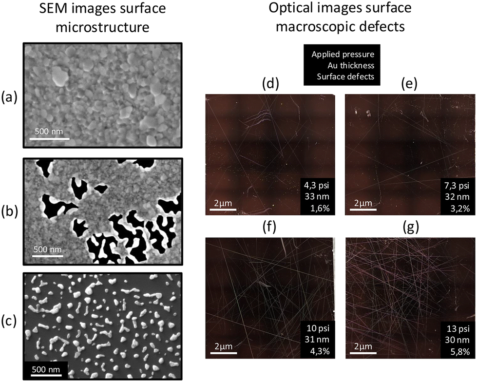 | ||
| Fig. 3 Microscopic and macroscopic Au film surface structure on 10 × 10 mm2 samples following abrasive-free CMP (a–c) SEM images of surface microstructure at different stages of CMP (bright areas: Au, dark areas: silicon substrate) (a) 70 nm thick gold film polished down to 20 nm, (b) additional polishing causing the removal of individual Au microcrystals resulting in aggregated holes that follow the grain boundaries, and (c) further polishing resulting in a discontinuous film where the remaining material forms isolated nanoscale Au islands; (d–g) Macroscopic surface defects (qualitative: scratches, quantitative: percentage of “bright” defect pixels) viewed by optical microscopy after CMP to reduce Au film thickness to ∼30 nm, at different applied pad pressures ((d) 4.3 psi; (e) 7.3 psi; (f) 10 psi; (g) 13 psi). CMP parameters: 1/200, 30 rpm, 50 mL min−1, room temperature (RT). | ||
Given the chemically dominated nature of the polishing process, the film microstructure is expected to have a significant impact on the results of the CMP process. The microstructure, particularly the grain size, is highly dependent on factors such as the nature of the substrate and deposited material stacks (metal and adhesion layers), the material deposition rates, and any thermal annealing steps. For example, we conducted thermal annealing on 70 nm thick gold films at 200 °C for 12 hours28 which resulted in a factor of 10 reduction in the MRR and increased inhomogeneity in material removal rate over the sample surface. Hence, the quantitative results presented here are specific to the experimental conditions and are meant to provide a foundation for further work, leading to a deeper understanding of CMP removal mechanisms under a variety of experimental conditions in relation to the material microstructure.
Macroscopic flaws such as localized defects (ex: scratches) or variations in the amount of material removed across the sample surface pose significant challenges for the fabrication by CMP of relatively large structures such electric interconnections or arrays of nanostructures. Typically, scratches and other such as localized defects arise from agglomerated abrasive particles in the slurry.16,29 Consequently, in the case of abrasive-free CMP, the incidence of such defects is expected to be comparatively lower.25Fig. 3d–g show optical images of 10 × 10 mm2 samples following CMP to reduce Au film thickness to ∼30 nm, at increasing applied pad pressures. The images show an increase in macroscopic surface defects, both qualitatively (number of scratches) and quantitatively (percentage of “bright” defect pixels), with increasing pad pressure. Indeed, a more intense contact between pad and sample heightens the force applied to free Au particles in contact with the surface and reduces the efficiency at which free particles are evacuated in the slurry. Since increased pad pressure does not result in significant increases in MRR (Fig. 2b), CMP at low pad pressure will minimize the density of such macroscopic defects. Finally, given the tunability of the MRR with slurry flow rate, pad rotation speed, and dilution factor, these parameters must be carefully set to strike a balance between the controllability of MRR (challenging for shorter polishing times) and defect density (higher with longer polishing times as shown qualitatively in ESI Fig. S3†).
Arrays of gold nano-cubes embedded in an SiO2 film
The proposed abrasive-free CMP method was used in a damascene process to fabricate arrays of gold nano-cubes (NCs) embedded in an SiO2 film. Using plasma etching, 45 nm deep square area wells were etched into the SiO2, followed by deposition of a 90 nm thick non-conformal Au layer by e-beam evaporation. Abrasive-free CMP was then used to remove the excess metal and achieve a final planar surface of Au squares embedded in the oxide film. Indeed, an important advantage of the abrasive-free nature of the method is its high selectivity between Au and SiO2, which was verified by subjecting a bare SiO2 film to aggressive CMP conditions without any measurable oxide removal (10 psi pressure, 60 rpm rotation speed, 1/50 slurry dilution, 100 mL min−1 flow, 150 s polishing time). In the experimental results discussed below, both the well area and array period were varied to study the impact on the fabrication of embedded NCs.Based on results from the previous section, CMP parameters were selected to achieve a MRR of 30–40 nm min−1, leading to polishing times of around 2–3 min (4.3 psi pressure, 30 to 60 rpm rotation speed, 1/200 slurry dilution, 50 mL min−1 flow). The surface profile of the wells ranged from 100 to 800 nm on a side. The array period was varied to span a range of pattern densities, that is, the final percentage of Au surface relative to the total surface area of the array (4% to 64%). The following gold embedded NC arrays in Fig. 4a–c are obtained after CMP.
 | ||
| Fig. 4 SEM images of gold nanocubes (NC) embedded in SiO2 revealed by abrasive-less CMP damascene fabrication for various device dimensions to illustrate (a–c) process capabilities and (d and e) cross section STEM images: (d) before and (e) after abrasive-free CMP. Initial Au film thickness: 390 nm; structured SiO2 substrate geometry: 130 nm deep 200 × 200 nm wells, 25% pattern density. The carbon (C) layer above the structures serves for protection during the FIB sample preparation. | ||
To have a better insight into the damascene process, Fig. 4d and e shows STEM (scanning transmission electron microscopy) cross-section images, before and after CMP, of a device based on NCs fabricated in an array of 200 × 200 nm2 wells with a 25% pattern density. In this case specifically, thicker more robust NCs were fabricated (130 nm deep wells, 390 nm thick Au film) to improve vertical facet quality for visualization by STEM after cross-sectioning by focused ion beam (FIB). Note that Au film growth by e-beam evaporation in nano-scale wells is a complex mechanism involving two distinct growth surfaces: at the bottom of the wells and on top of the unstructured SiO2 film (there is no growth from the vertical sidewalls due to the directional nature of the e-beam evaporation process).
Material removal and evolution of the overall surface profile during CMP were quantified by assessing the surface planarization, that is, the difference in average height between the areas above the unstructured SiO2 film and the areas above the wells containing the NCs. Fig. 5a shows a typical planarization curve over time illustrating the stages in the damascene process by abrasive-free CMP designed to reveal the NCs embedded in the SiO2 film with a final planar surface profile across the entire device (stages i to iv, the gray areas designate typical measurement variations across samples). Fig. 5b shows schematic side profile representations of unit cells in an array at different polishing times and stages along with representative AFM surface topology images (2 × 2 subarrays of NCs). Note that the reference height in the planarization calculation (the average surface height above the unstructured SiO2 surface) is not static but instead decreases gradually during the process until a bare unstructured surface SiO2 is reached (end of stage iii). During stage i for example, since the areas above the wells and the intervening surface (the reference) are both covered with Au, their respective heights decrease during polishing, as does the planarization (the difference between them). The planarization may be negative in stage iii if the remaining (very thin) Au film atop the unstructured SiO2 areas is either thinned more quickly or completely delaminates while the NCs have not yet been polished down to the same level.
 | ||
| Fig. 5 Process stages and process dynamics for abrasive-free CMP damascene fabrication of an array of NCs embedded in an SiO2 film. (a) typical planarization profile over time showing distinct stages; (b) schematic side profile of unit cells in the array at the different stages and polishing time with representative AFM surface topology images (2 × 2 subarrays of NCs with different NC size and array density, 400 nm scale bars); (c) planarization curves for different NC sizes in a 64% density array (the thicker colored areas represent measurement variations of height difference across the 4 × 4 subarray used); (d) initial planarization rates in stage i as a function of NCs size and array density. | ||
Planarization stages (Fig. 5):
i. Initial polishing to remove the surface topology of the metal film. An efficient CMP process exhibits a marked negative slope during this stage.
ii. Thinning of the planar gold surface, planarization is zero during this stage.
iii. Critical (under) polishing where the remaining thin Au film atop the unstructured SiO2 surface is removed. The NCs may protrude above the bare SiO2 surface at end of this stage (negative planarization) due to a combination of two factors:
a. In the final polishing stages, the Au film atop the SiO2 surface becomes discontinuous and eventually delaminates completely, as discussed previously.
b. The interfaces that form between the metal films grown from the bottom of the wells and from the unstructured SiO2 surface may be mechanically weaker than the grain boundaries. As a result, the final thin layer of Au film grown from the unstructured SiO2 surface may delaminate while the films grown from the bottom of the wells (the nearly completed NCs) remain relatively intact. The magnitude of this effect will be highly dependant on deposition conditions, as well as on array/well geometry as discussed below.
iv. Final polishing to remove the metal film topology above the wells, complete the forming of the NCs, and achieve a planar Au–SiO2 surface. Planarization reaches zero at the end of this stage.
v. Dishing of the NCs (left schematic) and partial/complete NC delamination due to over-polishing (right schematic).
Importantly, the dynamics and characteristics of the different stages vary with array geometry (well size and density). In stage i for example, planarization rate (slope of the initial linear portion of the curve) decreases with NC size and increases with array density (Fig. 5d). In stage ii, plateau duration decreases with NC size, to the point of being unmeasurable for 800 nm NCs in a 44% density array (Fig. 5c). In some cases of stage ii, a short positive spike appears in the plateau, during which time the topology is no longer flat because the Au film above the wells is again thinner than above the unstructured surface (black and red curves for 100 nm and 200 nm NCs in Fig. 5c). This effect is similar to the NC protrusions at the end of step iii, but in reverse, where the thin metal film remaining on top of the NCs that was grown from the neighboring unstructured SiO2 surface detaches first. In stage iii, array densities below 44% show no early elimination of the metal film above the unstructured surface (Fig. 5c). For extended polishing times in stage v, dishing is observed for all wells and array geometries (Fig. 5c and Fig. S4†).
Fig. S6a in ESI† shows that polishing times required for device completion ranged from 110 to 145 seconds for the various array geometries studied. Although increasing pad rotation speed did not result in any significant increase in the planarization rate at stage i (Fig. S5†). Final polishing times were reduced by ∼25% (Fig. S6b†), which correlates with the increase in MRR observed with un-patterned films (Fig. 2). Interestingly, optimal polishing times did not vary significantly with array density for NC size of 400 nm and below, indicating that the proposed abrasive-free CMP method can be used with standardized conditions and fabrication time for a wide range of device geometries. This is well illustrated in Fig. 4a–c where three different geometries (NC size and array) are fabricated on the same substrate by CMP. Finally, Fig. S7a–c† highlight typical fabrication defects that may occur during CMP parameter optimization and their possible causes: (a) residual Au on the SiO2 surface between NCs due to under-polishing; (b) excessive dishing of the NCs and/or delamination at the center of the wells due to slight over-polishing; (c) NC delamination due to excessive over-polishing and/or sub-optimal Au deposition parameters.
Fabrication of nanostructured plasmonic array over mirror, CMP vs. lift-off
The main motivation for this work was to develop an industrially compatible process for fabricating metal/dielectric optical nanostructures such as plasmonic nano-cavities. This section reports on a test structure comprised of an array of gold NCs embedded in SiO2 as described above, fabricated atop a continuous gold film (mirror) with an intervening 20 nm dielectric gap (SiO2 or Al2O3). The structure thus forms an array of plasmonic nano-cavities. Fig. 6a and d show the structure geometry and thin film stack (2 nm thickness metal/dielectric Ti adhesion layers shown in red), as well as the orientations of the excitation light incidence and electric field. Although similar structures have been fabricated by many other groups by lift-off30 and nanoparticle self-assembly,31 we now demonstrate that abrasive-free CMP is advantageous for fully embedding metal nanostructures in a dielectric film. | ||
| Fig. 6 Array of Au NCs embedded in SiO2 fabricated atop an Au mirror with a dielectric spacer. (a) and (d) top and side schematic representations; (b) and (c) SEM images of devices fabricated by abrasive-free CMP and lift-off; (e) and (f) corresponding AFM surface topology profiles along the dotted lines in (b) and (c); (g) reflection spectra at normal incidence in the visible range showing FDTD simulations with experimental measurements from the two fabrication methods. | ||
For comparison, the plasmonic nano-cavity arrays were fabricated both by lift-off and by abrasive-free CMP. Devices fabricated using the two methods appear quite similar in SEM images (Fig. 6b and c). However, AFM line profiles along the dotted lines labelled 1–3 in Fig. 6b and c show significant differences in surface topology. For CMP (Fig. 6e), a slight over-polishing resulted in the NCs being recessed below the surface by ∼5 nm rms. In the case of lift-off (Fig. 6f), the NCs had a positive profile and protruded above the surface by ∼15 nm rms. These results show that the proposed method is superior to lift-off for fabricating embedded metal/dielectric optical nanostructures in devices requiring a flat surface topology. Moreover, lift-off fabricated structures exhibit defects such as collar-shaped excess gold above the NCs which are absent after CMP as illustrated in Fig. S8 in ESI.†
Fig. 6g displays FDTD (finite difference time domain) simulations (details given in section Methods and fabrication), as well as experimental measurements for devices fabricated with both methods, of the reflection spectra under normal incidence from 400 nm to 900 nm. The spectra show a strong reflectance minimum at 725 nm indicative of a localized surface plasmon (LSP) mode in the NCs interacting with the mirror, known as a gap mode.30–32 This mode is characterized by a high field enhancement at the bottom edge of the NC and strong field confinement between the nanostructures and the mirror, as illustrated by the modeled field distribution in Fig. S9 in ESI.† Both measurement spectra show good correspondence with the numerical model, confirming successful fabrication of the nanostructure arrays.
Methods and fabrication
Fabrication and CMP methodology
All devices were fabricated on 10 × 10 mm2 Si substrates. For unstructured metal surfaces, experiments were carried out on 70 nm thickness Au films (2 nm Ti adhesion layer) deposited with an Edwards Auto 306 thermal evaporator. For the SiO2vs. Au selectivity measurement, a 55 nm thickness SiO2 film was deposited by PECVD at 250 °C on an Si substrate with a Benchmark 800-II plasma processing tool. For the damascene process, an SiO2 layer (100 nm or 200 nm thick) was first deposited by PECVD, followed by e-beam lithography at 100 keV using 80 nm thick ARP-6200(.04) CSAR positive resist with a Raith EBPG-5200. The exposed resist was developed in methyl-isobutyl-ketone (MIBK) for 1 min. The SiO2 etching was conducted with an inductively coupled plasma process33 in an STS Advanced Oxide Etching DRIE system. After stripping the resist, Au was deposited by evaporation using the Edwards system. CMP was performed in an Alpsitec E460 system with a 10 × 10 mm2 sample holder. The surface of the IC1000 polyurethane pad was prepared with a diamond conditioner before every polishing (moderate conditioning described in SI). The abrasive-free slurry was a TFA gold etchant solution from Transene CO Inc.26 diluted in deionized water at different concentrations. Every polishing stage was followed by two cleaning steps (20 and 40 s) of the sample with deionized water on the pad. The effect of pad conditioning was evaluated by comparing MRRs after low conditioning and moderate conditioning. Results in Fig. S1† show that pad conditioning had a negligible effect due to the lack of abrasive in the slurry.Nanostructured plasmonic array over mirror fabrication (CMP and lift-off)
The nanostructured plasmonic arrays over a gold mirror were fabricated by CMP and lift-off. Gold patterning steps were common to both methods. Using an Intelvac e-beam evaporation system, 50 nm thick Au layers were deposited on Si substrates. Without breaking vacuum, a 60 nm thickness SiO2 layer was deposited then by sputtering. Adhesion layers (2 nm Ti) were used at both the Si/Au and SiO2/Au interfaces. E-beam lithography was performed with 200 nm thick ARP-6200 CSAR positive resist with a Raith EBPG-5200 at 100 keV. The exposed resist was developed in MIBK for 1 min. Etching of SiO2 was achieved with an inductively coupled plasma process33 in an STS Advanced Oxide Etching DRIE system. For CMP, the process described above was used. For lift-off, the resist used at the etching step was used to selectively deposit 50 nm Au in the SiO2 wells by e-beam evaporation. The samples are then immersed in acetone for 2 h and sonicated for 1 min to enhance lift-off efficiency, followed by cleaning with isopropanol and water.Surface topology characterization
Au film thickness was measured by ellipsometry with a J.A. Woollam Alpha-SE tool using a model of Au thin films based on experimental data acquired from a range of Au films deposited in the same conditions in our facilities. Nanoscale imaging and topology measurements were performed with a Thermofisher Apreo2 SEM and a Park System NX20 AFM, respectively. Device cross section images were acquired with STEM after milling and thinning a 10 × 5 μm2 portion of a sample down to less than 100 nm lateral thickness by FIB in a Thermofisher Scios SEM. Optical images were obtained with a Keyence VK-X1100 confocal microscope. Planarization was assessed by AFM topology measurement from samples removed from the CMP process at regular time intervals, i.e. each sample point in Fig. 5c correspond to one device from the same fabrication run that were removed from the fabrication sequence for measurement.Plasmonics response characterization
Measurement of the array plasmonic response is performed in the far-field with a reflection setup in the visible range. Light emitted by a halogen lamp passing through a IHR 320 monochromator and a linear polarizer (polarization parallel to the Si substrate plane) is incident onto the sample surface at normal incidence. The reflected light is collected by a non-polarizing beam splitter and CMOS camera at each wavelength selected by the monochromator. Spectra are extracted by the average signal level of the image in the structured areas and normalized by the average signal level in the unstructured areas, for each wavelength.FDTD simulations
Electromagnetic simulations of the nanostructured plasmonic arrays were performed with the Ansys Lumerical FDTD software. Periodic boundary conditions were applied in the directions perpendicular to the film plane at the edge of the modeling domain. Perfectly matched layer (PML) boundary conditions were applied in the directions parallel to the film plane at the edge of the modeling domain. Geometry and dimensions of the structure are given in Fig. 6a&d. The optical index of gold is based on experimental data acquired from a range of Au films deposited in our facilities. Modeled reflection values were normalized by results from same model without nanostructures to be comparable with experimental results.Conclusions
This work presented a study of an industry compatible and robust method for gold film nanostructuring using an abrasive-free CMP approach. The process achieves consistent results and limited defects with a highly tunable material removal rate (MRR) by varying the slurry concentration (diluted gold etchant in water). Exploring the effects of CMP parameters on the MRR, we determined that the polishing mechanism for gold involves both chemical alteration of the microstructure and removal of grains through the mechanical action of the pad. Fabrication of millimeter-scale devices featuring nanostructure arrays with elements ranging from 100 nm to 1 μm in size was achieved. The experiments demonstrated a high planarization rate, efficiently removing excess gold deposited in SiO2 wells and resulting in a highly planar surface with embedded gold nanostructures. The geometry of the arrays, including feature size and array density, significantly influenced the various stages of planarization during the damascene process. The effectiveness of the abrasive-free CMP process was further validated by fabricating plasmonic nanocavities consisting of gold nanostructure arrays over a gold mirror that exhibited high-contrast resonance in the visible range, aligning well with simulation results. Compared to lift-off, abrasive-free CMP is more effective for embedding Au nanostructures in a dielectric film to achieve a flat device surface topology.Author contributions
RG: conceptualization, software, formal analysis, validation, investigation, visualization, methodology, writing – original draft, writing – review & editing. GB, JFB: resources, data curation, writing – review & editing; RS: methodology; PL, FF, SGM: conceptualization, resources, supervision, funding acquisition, project administration, writing – review & editing; DD: conceptualization, resources, supervision, project administration; PGC, SE: conceptualization, resources, data curation, supervision, funding acquisition, methodology, writing – review & editing, project administration.Data availability
Data for this article are available at Replication data for “Abrasive-free chemical-mechanical planarization (CMP) of gold for thin film nano-patterning” at https://doi.org/10.5683/SP3/60ZFJP. Data supporting this article have also been included as part of the ESI.†The datas have been submitted for revision to the student dataverse of Université de Sherbrooke in Borealis. Follow this link to access the data before submission is completed: https://borealisdata.ca/dataset.xhtml?persistentId=doi:10.5683/SP3/60ZFJP.
Raphael Gherman & Serge Ecoffey.
Conflicts of interest
There are no conflicts of interest to declare.Acknowledgements
This work was supported by the Natural Sciences and Engineering Research Council of Canada (NSERC) and Infinite Potential Laboratories LP. (Waterloo, ON). We would like to acknowledge CMC Microsystems for financial assistance via the MNT Award.LN2 is a French-Canadian joint International Research Laboratory (IRL 3463) funded and co-operated by CNRS, Université de Sherbrooke, INSA Lyon, École Centrale Lyon (ECL) as well as Université Grenoble Alpes (UGA). It is also supported by the Fonds de Recherche du Québec Nature et Technologie (FRQNT). LN2 is principally operated at the Institut Interdisciplinaire d'Innovations Technologiques (3IT) at Sherbrooke.
Infinite Potential Laboratories LP (IPL) is a company under the umbrella of Quantum Valley Investments located in Waterloo, Ontario, that supports research and commercialization activities associated with Quantum Information Science. IPL wishes to take advantage of the latest progress in quantum materials and nano-fabrication science to develop new technologies for vacuum-based applications in quantum information processing.
References
- T.-S. Choi and D. W. Hess, ECS J. Solid State Sci. Technol., 2015, 4, N3084–N3093 CrossRef CAS.
- M. Hoshino, H. Suehiro, K. K. K. Kasai and J. K. J. Komeno, Jpn. J. Appl. Phys., 1993, 32, L392 CrossRef CAS.
- H. Ishii, S. Yagi, T. Minotani, Y. Royter, K. Kudou, M. Yano, T. Nagatsuma, K. Machida and H. Kyuragi, Gold damascene interconnect technology for millimeter-wave photonics on silicon, Proc. SPIE 4557, Micromachining and Microfabrication Process Technology VII, 2001, DOI:10.1117/12.442947.
- M. De Lafontaine, T. Bidaud, G. Gay, E. Pargon, C. Petit-Etienne, A. Turala, R. Stricher, S. Ecoffey, M. Volatier, A. Jaouad, C. E. Valdivia, K. Hinzer, S. Fafard, V. Aimez and M. Darnon, Cell Rep. Phys. Sci., 2023, 101701 CrossRef CAS.
- A. Barik, X. Chen and S.-H. Oh, Nano Lett., 2016, 16, 6317–6324 CrossRef CAS PubMed.
- S. A. Maier, Plasmonics: Fundamentals and Applications, Springer, 1st edn., 2007 Search PubMed.
- T. A. Green, Gold Bull., 2014, 47, 205–216 CrossRef CAS.
- H. J. Fan, P. Werner and M. Zacharias, Small, 2006, 2, 700–717 CrossRef CAS.
- V. Mulloni, B. Margesin, P. Farinelli, R. Marcelli, A. Lucibello and G. De Angelis, Microsyst. Technol., 2017, 23, 3843–3850 CrossRef CAS.
- K. R. Williams, K. Gupta and M. Wasilik, J. Microelectromech. Syst., 2003, 12, 761–778 CrossRef CAS.
- O. Vazquez-Mena, L. Gross, S. Xie, L. G. Villanueva and J. Brugger, Microelectron. Eng., 2015, 132, 236–254 CrossRef CAS.
- C.-C. Yu and H.-L. Chen, Microelectron. Eng., 2015, 132, 98–119 CrossRef CAS.
- M. T. Do, Q. C. Tong, A. Lidiak, M. H. Luong, I. Ledoux-Rak and N. D. Lai, Appl. Phys. A, 2016, 122, 360 CrossRef.
- M. S. Miller, M.-A. Ferrato, A. Niec, M. C. Biesinger and T. B. Carmichael, Langmuir, 2014, 30, 14171–14178 CrossRef CAS.
- G. Karbasian, P. J. Fay, H. G. Xing, A. O. Orlov and G. L. Snider, J. Vac. Sci. Technol. A, 2014, 32, 021402 CrossRef.
- M. Merhej, D. Drouin, B. Salem, T. Baron and S. Ecoffey, Microelectron. Eng., 2017, 177, 41–45 CrossRef CAS.
- R. Stricher, A. Elshaer, D. Drouin and S. Ecoffey, 23rd International Symposium on Chemical-Mechanical Planarization, Lake Placid NY, United States, 2019, p. 22 Search PubMed.
- N. K. Penta, in Advances in Chemical Mechanical Planarization (CMP), Elsevier, 2016, pp. 213–227 Search PubMed.
- N. K. Penta, P. R. D. Veera and S. V. Babu, ACS Appl. Mater. Interfaces, 2011, 3, 4126–4132 CrossRef CAS.
- N. K. Penta, P. R. Dandu Veera and S. V. Babu, Langmuir, 2011, 27, 3502–3510 CrossRef CAS.
- S. B. S. V. Janjam Ph.D., Chemical mechanical polishing of tantalum and tantalum nitride, Clarkson University, 2009 Search PubMed.
- H. P. Amanapu, K. V. Sagi, L. G. Teugels and S. V. Babu, ECS J. Solid State Sci. Technol., 2013, 2, P445 CrossRef CAS.
- B. C. Peethala and S. V. Babu, J. Electrochem. Soc., 2011, 158, H271 CrossRef CAS.
- S. Pandija, D. Roy and S. V. Babu, Mater. Chem. Phys., 2007, 102, 144–151 CrossRef CAS.
- S. Kondo, N. Sakuma, Y. Homma, Y. Goto, N. Ohashi, H. Yamaguchi and N. Owada, J. Electrochem. Soc., 2000, 147, 3907–3913 CrossRef CAS.
- Gold Etchants | Transene, https://transene.com/au-etchant/, (accessed 5 March 2024).
- Y. Moon, in Advances in Chemical Mechanical Planarization (CMP), ed. S. Babu, Woodhead Publishing, 2nd edn., 2022, pp. 3–28 Search PubMed.
- D. Porath, E. Bar-Sadeh, M. Wolovelsky, A. Grayevsky, Y. Goldstein and O. Millo, J. Vac. Sci. Technol. A, 1995, 13, 1165–1170 CrossRef CAS.
- U. Paik and J.-G. Park, Nanoparticle engineering for chemical-mechanical planarization: fabrication of next-generation nanodevices, CRC Press/Taylor & Francis Group, Boca Raton, FL, 2009 Search PubMed.
- Z. Wang, L. Li, S. Wei, X. Shi, J. Xiao, Z. Guo, W. Wang, Y. Wang and W. Wang, J. Appl. Phys., 2023, 133, 063101 CrossRef CAS.
- Q.-Y. Lin, Z. Li, K. A. Brown, M. N. O'Brien, M. B. Ross, Y. Zhou, S. Butun, P.-C. Chen, G. C. Schatz, V. P. Dravid, K. Aydin and C. A. Mirkin, Nano Lett., 2015, 15, 4699–4703 CrossRef CAS PubMed.
- H. Saito, D. Yoshimoto, H. Lourenco-Martins, N. Yamamoto and T. Sannomiya, ACS Photonics, 2019, 6, 2618–2625 CrossRef CAS.
- M. Guilmain, A. Jaouad, S. Ecoffey and D. Drouin, Microelectron. Eng., 2011, 88, 2505–2508 CrossRef CAS.
Footnote |
| † Electronic supplementary information (ESI) available: Experimental details and results of the effect of the conditioning of the pad, calculation of the error on CMP parameters and MRR, experimental removed gold thickness as a function of polishing time for various CMP parameters and list of full CMP parameters for the different experiments, effect of polishing time on macroscopic defects and scratches, additional planarization curve for various geometries and two pad rotation speed, microscopic observation of gold NCs embedded in SiO2, simulated optical reflectivity of gold NC over mirror array and electric field distribution. See DOI: https://doi.org/10.1039/d4nr02610a |
| This journal is © The Royal Society of Chemistry 2024 |