
New paradigms of 2D layered material self-driven photodetectors
Xinyi
Guan†
 a,
Yu
Chen†
a,
Yuhang
Ma
a,
Huanrong
Liang
a,
Zhaoqiang
Zheng
b,
Churong
Ma
c,
Chun
Du
c,
Jiandong
Yao
*a and
Guowei
Yang
a
a,
Yu
Chen†
a,
Yuhang
Ma
a,
Huanrong
Liang
a,
Zhaoqiang
Zheng
b,
Churong
Ma
c,
Chun
Du
c,
Jiandong
Yao
*a and
Guowei
Yang
a
aState Key Laboratory of Optoelectronic Materials and Technologies, Nanotechnology Research Center, Guangzhou Key Laboratory of Flexible Electronic Materials and Wearable Devices, School of Materials Science & Engineering, Sun Yat-sen University, Guangzhou 510275, Guangdong, P. R. China. E-mail: yaojd3@mail.sysu.edu.cn
bSchool of Materials and Energy, Guangdong University of Technology, Guangzhou 510006, Guangdong, P. R. China
cGuangdong Provincial Key Laboratory of Optical Fiber Sensing and Communications, Institute of Photonics Technology, Jinan University, Guangzhou 511443, Guangdong, P. R. China
First published on 24th October 2024
Abstract
By virtue of the high carrier mobility, diverse electronic band structures, excellent electrostatic tunability, easy integration, and strong light-harvesting capability, 2D layered materials (2DLMs) have emerged as compelling contenders in the realm of photodetection and ushered in a new era of optoelectronic industry. In contrast to powered devices, self-driven photodetectors boast a wealth of advantages, notably low dark current, superior signal-to-noise ratio, low energy consumption, and exceptional compactness. Nevertheless, the construction of self-driven 2DLM photodetectors based on traditional p–n, homo-type, or Schottky heterojunctions, predominantly adopting a vertical configuration, confronts insurmountable dilemmas such as intricate fabrication procedures, sophisticated equipment, and formidable interface issues. In recent years, worldwide researchers have been devoted to pursuing exceptional strategies aimed at achieving the self-driven characteristics. This comprehensive review offers a methodical survey of the emergent paradigms toward self-driven photodetectors constructed from 2DLMs. Firstly, the burgeoning approaches employed to realize diverse self-driven 2DLM photodetectors are compiled, encompassing strategies such as strain modulation, thickness tailoring, structural engineering, asymmetric ferroelectric gating, asymmetric contacts (including work function, contact length, and contact area), ferroelectricity-enabled bulk photovoltaic effect, asymmetric optical antennas, among others, with a keen eye on the fundamental physical mechanisms that underpin them. Subsequently, the prevalent challenges within this research landscape are outlined, and the corresponding potential approaches for overcoming these obstacles are proposed. On the whole, this review highlights new device engineering avenues for the implementation of bias-free, high-performance, and highly integrated 2DLM optoelectronic devices.
 Jiandong Yao | Jiandong Yao received his B.S. degree in Materials Physics in 2013 and his Ph.D. degree in Condensed Matter Physics in 2018 from Sun Yat-sen University. After being a Research Fellow of Nanyang Technological University, he joined School of Materials Science & Engineering, Sun Yat-sen University as an Associate Professor. His research endeavors encompass the controllable synthesis of low-dimensional materials as well as their innovative application within the realm of optoelectronics. |
1. Introduction
The revolutionary exfoliation of graphene by Novoselov & Geim in 2004 opened the prelude to the exploration of two-dimensional layered materials (2DLMs).1 Broadly speaking, 2DLMs encompass ultrathin nanosheets/nanofilms composed of a solitary monolayer or a few monolayer motifs held together by feeble van der Waals interactions.2–14 Up to now, 2DLMs have exhibited a host of unique physical and chemical properties, such as high surface-to-volume ratio, large interlayer spacing, easy integration, excellent flexibility, etc., which make them widely applicable in extensive research fields spanning electronics,15–17 information storage,18 photonics,19–25 medical therapy,26 energy storage,27–30 catalysis,31–33 electromagnetic shielding,34 assisted driving,35 superconductivity,36–38etc.In recent years, by virtue of the high carrier mobility, diverse electronic band structures, excellent electrostatic tunability, and strong light-harvesting capability, 2DLMs have been highly regarded and demonstrated remarkable potential in the field of photodetection.39–46 Generally speaking, 2DLM photodetectors can be largely divided into two main categories, including powered devices and self-driven devices. Powered photodetectors are devices that necessitate the impetus of external auxiliary power sources for normal operation.47–66 The most common powered photodetectors include metal–semiconductor (semimetal)-metal (MSM) photoconductors and phototransistors.67,68 By contrast, self-driven photodetectors refer to devices that can operate normally without the propulsion of any external power sources. Compared to powered devices, self-driven photodetectors bear a series of advantages. To begin with, due to the absence of an external driving electric field, the dark current of the self-driven devices is extremely low, resulting in a remarkable signal-to-noise ratio and low energy consumption. Secondly, devoid of the intricate power systems, self-driven photodetectors typically exhibit simpler constructions, rendering them not only more compact and reliable but also significantly easier to maintain. This proves exceptionally advantageous in circumstances where a sustained power supply to the photodetectors is impractical, notably in realms such as remote sensing, wearable electronic devices, and Internet of Things (IoT). Thirdly, owing to the exemption of any power supply, the electromagnetic radiation emitted during the operation of self-driven photodetectors is notably feeble, making them more difficult to be detected. This exceptional level of concealment is paramount across diverse fields such as military reconnaissance and intelligence gathering, helping to reduce the risk of exposure and bolster the mission success rate. Furthermore, apart from the incident light energy, self-driven photodetectors operate without consuming electricity or any other forms of energy, which is highly environmentally friendly.
Basically, a bias-free photodetector is mainly constructed based on a p–n junction69–72 or a Schottky junction.73–75 However, self-driven photodetectors built of traditional p–n or Schottky junctions, which are mostly in a vertical form, suffer from a host of shortcomings. To begin with, due to the extremely thin thickness, 2DLMs are far less robust as compared to bulk counterparts. In this consideration, traditional doping processes, such as ion implantation, are quite harmful to 2DLMs. To date, the mature technologies of chemical doping for 2DLMs are not yet established. Secondly, it is difficult to precisely control the doping depth by exploiting traditional doping techniques as for the atomically thin materials, making it challenging to achieve controllable preparation of atomically thin p–n junctions. Thirdly, the output signal of p–n junctions is intrinsically limited by the Shockley–Queisser limit. Therefore, it is impending to relentlessly resort to novel schemes for overcoming the above difficulties.
In recent years, researchers all around the world have been striving to exploring alternative strategies for realizing self-driven photodetection based on 2DLMs through device engineering. For example, in 2018, Zhou et al. demonstrated zero-bias metal–semiconductor-metal WSe2 photodetectors by exploiting asymmetric contact geometries.76 In 2022, Lu et al. developed self-driven MoS2 homojunction photodetector by utilizing localized strain engineering.77 Most recently, by exploiting thickness tailoring, Hu et al. have successfully fabricated a bias-free MoT2 homojunction photodetector array.78
Despite that encouraging research progress has been achieved, the preceding research findings are extensive but relatively scattered. In addition, the underlying physical principles for implementing the self-driven operation of different studies are notably distinct. These diverse ingredients pose tricky dilemmas for researchers in swiftly attaining a comprehensive and profound understanding on this rapidly expanding research domain.
In this review, a systematic overview on the new device engineering paradigms of self-driven photodetectors built of 2DLMs has been provided. Firstly, the emerging strategies for realizing various self-driven 2DLM photodetectors have been epitomized, including strain modulation, thickness tailoring, structural engineering, asymmetric ferroelectric gating, asymmetric contacts (including work function, contact length, and contact area), ferroelectricity-enabled bulk photovoltaic effect, asymmetric optical antennas, etc., with the elaboration on the fundamental physical principles. Following this, the prevailing challenges standing in the way of this research realm have been identified, and potential solutions addressing them have been proposed. On the whole, this review outlines a fascinating blueprint for the implementation of self-driven, high-performance, and highly integrated optoelectronic devices.
2. Strain-enabled homojunction photodetectors
As mentioned in the previous section, most self-driven 2DLM photodetectors have been constructed based on heterojunctions (e.g., p–n junctions & Schottky junctions & homo-type junctions), where built-in electric field is formed on account of differentiated Fermi levels and photogenerated electron–hole pairs can be spontaneously separated with this impetus. However, 2DLM based heterojunctions commonly suffer from poor interface quality on account of a plethora of ingredients, such as loose interfacial contact by manual staking, serious interfacial contamination induced by transfer processing, and strong Fermi level pinning effects caused by interfacial defect states, making it quite challenging to achieve high-performance bias-free photodetection. Therefore, in recent years, researchers have been dedicated to exploring the transfer-free construction of 2DLM homojunctions. As is well known, the electronic band structure of low-dimensional materials is highly sensitive to strain.79–82 For example, density functional theory calculations have determined that the bandgap size of MoTe2 reduces markedly from 1.04 to 0.8 eV as the strain increases from 0 to 4%.79 In addition, first-principles calculations have found that both conduction band minimum and valence band maximum of Bi2S3 monotonously downshift with increasing strain from 0 to 8%.80 In this consideration, theoretically, the preparation of 2DLM homojunction zero-bias photodetectors can be achieved through rational strain engineering.For this purpose, in 2022, Lu and collaborators prepared a strained MoS2/MoS2 homojunction self-driven photodetector by partially integrating monolayer MoS2 on top of prefabricated Au nanoparticals (NPs), as schematically shown in Fig. 1a.77 Within this device structure, a portion of the monolayer MoS2 is shored up by the NPs underneath, leading to large biaxial tensile strain. As shown in Fig. 1b, under 660 nm illumination, pronounced photocurrent has been generated even at zero bias voltage. To further explore the physical mechanism of self-driven photodetection, first-principles calculations on the electronic band structures have been conducted (Fig. 1c). As the biaxial tensile strain increases, both the conduction band minimum (CBM) and valence band maximum (VBM) will downshift. As a consequence, a type-II band alignment has been formed between strained MoS2 and pristine MoS2. In addition, the Fermi level largely upshifts with increasing strain. Therefore, a built-in electric field pointing from strained MoS2 to pristine MoS2 is generated, as evidenced by the KPFM measurement (Fig. 1d and e). Upon light excitation, electron–hole pairs are generated. Under the drive of the type-II band alignment and the built-in electric field, electrons are driven to the strained MoS2, and holes are driven to the pristine MoS2, thus leading to the self-driven photoresponse (Fig. 1f). On the whole, this study provides a facile route to realize bias-free homojunction photodetectors with seamless and contamination-free interfaces, which is conductive to suppressing the recombination and accelerating spacial separation of photogenerated electron–hole pairs. Furthermore, the electronic band structures of a wealth of 2DLMs, such as CrI3,83 CrS2,84 blue phosphorene,85 ZrSe3,86 InSe,87 violet phosphorus,88etc., have been revealed to be highly dependent on strain. In this consideration, the strain engineering strategy herein holds broad university on constructing various self-driven 2DLM homojunction photodetectors, which are in need of further exploration in the upcoming future. Of note, a severe challenge for strain engineering is that the weak van der Waals force between 2DLM and substrate makes interlayer slippage easily occurs, resulting in inefficient strain transfer. To address this issue, coating the 2DLM channel with an encapsulation layer can be exploited, where the additional adhesion force supplied by the capping layer aids in stabilizing the 2DLM channel.89
 | ||
| Fig. 1 (a) Schematic of the Au nanoparticles/MoS2 (strained MoS2) and pristine MoS2 in-plane homojunction self-driven photodetector. (b) I–V curves of the strained MoS2/MoS2 in-plane homojunction photodetector in darkness (black line) and under 660 nm illumination (red line). (c) Calculated conduction band minimum (EC), valence band maximum (EV), and Fermi level (EF) of MoS2 as a function of biaxial tension strain. (d) KPFM image of the in-plane homojunction. (e) Height (bottom panel) and surface potential (top panel) line profiles along the blue dotted line in (d). (f) Energy band diagram of the self-driven strained MoS2/MoS2 homojunction photodetector under illumination. Reproduced from ref. 77 with permission from John Wiley and Sons, Inc, copyright 2022. | ||
3. Homojunction photodetectors via thickness tailoring
As previously stated, the majority of self-driven 2DLM photodetectors have been constructed based on van der Waals heterojunctions, intricate structures forged from two or more constituent components. Nevertheless, heterostructures have been commonly plagued by lattice mismatch, which engenders interfacial defects and distortions in the heterointerface. This, in turn, intensifies the trapping, scattering, and recombination of photocarriers, hindering the interfacial transport. Most notably, the traditional fabrication processes for preparing 2DLM-based heterojunctions, which frequently involve micromechanical exfoliation and transfer techniques, will inevitably introduce severe interfacial contamination, further degrading the device performances. These limitations significantly curtail the applicability of van der Waals heterojunctions in self-driven optoelectronic systems. In response to these tangible challenges, an ever-increasing number of researchers have turned their attention towards investigating and developing 2DLM homojunctions in a transfer-free manner, which feature seamless interfaces that function as ideal carrier transport pathways in optoelectronic devices.Traditionally, 2DLM homojunctions have been prepared through localized doping.90,91 However, the implantation of exotic atoms can probably cause degeneration of crystal properties on account of the inconsistent atomic diameter and electronegativity of the doped atoms as compared to the substituted atoms. In addition, the invasive doping process may also bring about serious crystal defects spanning vacancies, antistites, and intercalated atoms. Contact doping is another potential strategy.92–94 Nevertheless, a substantial proportion of these dopants exhibit relatively poor stability. In this consideration, the long-term reliability of related homojunction devices still needs further improvement. Electrostatic doping, which is usually realized by using split gates,95–101 can avoid the adverse effects caused by heteroatom doping and the instability of surface modification doping, but this scheme entails additional voltage sources, which makes the devices suffer from large volume as the powered devices. Furthermore, the extra gate capacitance may crop the response. In addition to doping and electrostatic gating, thickness is also an important element affecting the electronic band structure of 2DLMs. For example, both density functional theory and GW calculations have unveiled that the work functions of transition-metal dichalcogenides have close relationship with the thickness.102 In addition, first-principles calculations indicate that the bandgap of AgInP2S6 monotonously increases with decreasing thickness.52 Therefore, the construction of 2DLM homojunctions via thickness tailoring warrants a new avenue.
As a proof, in 2024, Hu and coresearchers reported on the preparation of pristine MoTe2 homojunction self-driven photodetectors via thickness tailoring.78Fig. 2a interprets the detailed preparation procedures. First, the molybdenum precursor nanofilms with asymmetric thicknesses are patterned on sapphire substrates using two-step photolithography and magnetron sputtering processes. Then, the MoTe2 homojunctions are achieved via tellurization of the molybdenum patterns using a chemical vapor deposition method. As shown in Fig. 2b, under illumination, net positive photocurrent generates, demonstrating the feasibility for zero-bias photodetection. Importantly, the photoresponse is stable and highly reversible under periodic illuminations with various light power (Fig. 2c). In order to garner an in-depth understanding on the underlying working mechanism, DFT calculations have been performed. As shown in Fig. 2d, as the thickness increases, the bandgap of MoTe2 decreases, leading to the shift of Fermi level. Consequently, a homojunction is formed between MoTe2 layers with various thicknesses, with the built-in electric field pointing from thick-MoTe2 to thin-MoTe2 (Fig. 2e). When the homojunction is illuminated with light, electrons in the valence band are excited to the conduction band, generating electron–hole pairs. Then, under the drive of the built-in electric field, the photogenerated electrons transport from thin-MoTe2 to thick-MoTe2, while photogenerated holes migrate from thick-MoTe2 to thin-MoTe2, thereby resulting in the generation of photocurrent. Taking advantage of the superior scalability of the mature fabrication process for patterning metal pads, a 10 × 10 MoTe2 homojunction photodetector array has been successfully constructed and harnessed for multi-pixel optoelectronic imaging (Fig. 2f). In conclusion, this finding spotlights a unique paradigm for the fabrication of bias-free 2DLM homojunction photodetectors precluding interface problems, thereby forging a path towards the realization of integrated and miniaturized photodetector systems featuring low energy consumption. By using the analogous working principle, a series of self-driven 2DLM homojunction photodetectors based on various 2DLMs, such as MoS2,103,104 MoSe2,105,106 WSe2,107 and ReS2,108 have been successfully constructed via thickness tailoring, underscoring the broad universality. Of note, most of the previous studies have been conducted based on micromechanical exfoliation technology, which, however, suffers from poor repeatability and controllability, making it impractical for practical application. Although the above two-step chemical vapor deposition method boasts commendable controllability, it falls short in terms of the interface quality of the resultant homojunction, exhibiting an unfavorable polycrystalline nature.78 Fortunately, a promising two-step oxidation-etching methodology has demonstrated remarkable efficacy in achieving layer-by-layer thinning of 2DLMs with atomic-level precision.109 Looking ahead, this technology can be further developed for constructing self-driven 2DLM homojunction photodetectors to achieve scalable and controllable customization of devices.
 | ||
| Fig. 2 (a) Schematic of the fabrication processes for preparing MoTe2 homojunctions via thickness engineering. (b) Output curves of the MoTe2 homojunction device in darkness and under 1060 nm light illumination with different light power. (c) Photoswitching curves under periodic 1060 nm illuminations with different light power under zero bias. (d) Bandgap as a function of layer number of MoTe2 based on DFT calculations (blue diamonds and line). (e) Schematic diagrams of the energy band structures of thin-MoTe2 and thick-MoTe2 before and after contact (left panel) as well as the carrier dynamics of the thin-MoTe2/thick-MoTe2 homojunction upon light excitation (right panel). (f) Schematic illustration of the imaging process based on the MoTe2 homojunction photodetector array. Reproduced from ref. 78 with permission from John Wiley and Sons, Inc, copyright 2024. | ||
4. Homojunction photodetectors by structural engineering
In general, self-driven photodetection has been largely relied on the formation of built-in electric field, which usually exists at the heterojunctions, typically p–n junctions,110 Schottky junctions,111,112 as well as homo-type junctions (i.e. n–n and p–p structures).113–115 However, there exist a host of drawbacks for 2DLM based heterostructures, including interfacial defects/deformation brought by lattice mismatch, large interfacial gap brought by the weak interlayer adhesion, interfacial impurities brought by mechanical exfoliation/transfer processing, etc. Despite that heterojunctions can be constructed by an in situ approach, epitaxial growth of van der Waals heterojunctions is quite challenging due to the high energy barrier required for nucleation and growth on the naturally passivated surface of 2DLMs compared with the conventional covalent materials.116 Within the context of the severe challenges in preparing heterostructures, the development of exceptional strategies aimed at the construction of built-in electric field is imperative and indispensable.As a prototypical example, most recently, Zhang et al. have harnessed neoteric self-assembled 1D/2D WSe2 homojunctions connected seamlessly by robust covalent bonds and exploited these structures for photodetection without external power.117 The detailed fabrication process has been schematically shown in Fig. 3a, which contains the deposition and rolling-up steps. Firstly, 2D morphological WSe2 nanosheets are prepared on SiO2/Si substrates via a chemical vapor deposition (CVD) method. Then, volatile solution (typically alcohol) is dripped onto the substrate. The solution molecules can readily penetrate into the interspace between the WSe2 nanosheets and the substrate and induce the dissociation. Following this, a spontaneous rolling-up process will occur under the drive of the surface tension.118,119 Of note, the area or degree of sample curling can be precisely controlled by the amount of alcohol solution, thus enabling the self-assembled construction of 1D/2D homostructures. As shown in Fig. 3b, first-principles calculations consolidate that the electronic band structures of 2D WSe2 and 1D WSe2 are highly distinct, which lays a solid foundation for self-driven photodetection. Fig. 3c showcases the schematic diagram of a WSe2 homojunction photodetector, where a heterogeneous interface is formed between 1D WSe2 and 2D WSe2. Specifically, this homojunction is tightly connected by robust covalent bonds rather than feeble vdW interactions of the traditional heterostructures, which avoids the excessive interfacial gap as well as the damage of defects, impurities and dangling bonds. Thus, the self-assembled 1D/2D homojunction offers an efficient interfacial charge transfer channel, which is conducive to high photosensitivity and speed. As depicted in Fig. 3d, under zero bias condition, the 1D/2D homojunction photodetector exhibits a pronounced photoresponse to periodic 660 nm illumination, in stark contrast to the negligible photoresponse displayed by both the 1D WSe2 (curling degree of ≈100%) and 2D WSe2 photodetectors (curling degree of ≈0%). These results suggest that the self-driven characteristics are induced by the unique composite 1D/2D homojunction structure. According to the DFT calculations, the Fermi level of 1D WSe2 is higher than that of 2D WSe2. As a consequence, a built-in electric field pointing from the former to the latter is formed after these components are in contact. Upon light excitation, photocarriers are generated, after which electrons drift to the 1D WSe2 while holes drift to the 2D WSe2 under the drive of the built-in electric field, thereby resulting in the self-driven photoresponse. As shown in Fig. 3e, the WSe2 homojunction device possesses fast response rate, with the rise and decay time reaching 23.1 ms and 16.8 ms, respectively. Most importantly, by virtue of the strong anisotropy of 1D WSe2, the homojunction device exhibits pronounced polarized photosensitivity. As clearly shown in Fig. 3f and g, the photocurrent exhibits approximate periodic variation with changing polarization angle and reaches the maximum/minimum magnitude at 0°/90°. Specifically, a dichroic ratio up to ≈2.02 has been achieved under 638 nm illumination, which demonstrates a competitive polarization sensitivity. In general, the study depicts an innovative protocol towards homojunction photodetectors featuring intact interface as well as exceptional functionality, opening up new opportunities for highly integrated and multifunctional photoelectric detection.
 | ||
| Fig. 3 (a) Schematic diagrams of the fabrication processes for constructing the 1D/2D WSe2 homojunctions via a self-assembled strategy. (b) Band structures of 1D WSe2 (left panel) and 2D WSe2 (right panel) extracted from theoretical calculations. (c) Schematic diagram of a 1D/2D WSe2 homojunction photodetector. The inset in the top-left corner shows an optical microscope image. (d) Photoswitching curves of the 1D WSe2 (red line), 2D WSe2 (green line), and 1D/2D WSe2 homojunction (orange line) photodetectors under periodic illumination at zero bias. (e) The response time and decay time. (f) Anisotropic photoresponse of the 1D/2D WSe2 homojunction device at zero bias under linearly polarized 638 nm illumination. (g) Polar plot of the photocurrent as a function of polarization angle, the angle between the 1D WSe2 and the polarization direction of incident light. Reproduced from ref. 117 with permission from American Chemical Society, copyright 2024. | ||
5. Homojunction photodetectors induced by asymmetric nonvolatile ferroelectric gating
Due to the atomic-level channel thickness, the electrostatic screening ability of 2DLMs is extremely feeble. In this consideration, the polarity of charge carriers of 2DLMs can be flexibly controlled by the electrostatic field of the gate. On this basis, the preparation of 2DLM p–n homojunctions can be achieved through localized regulation of the gate voltage, providing an efficient strategy for realizing zero-bias photoelectric detection. In reality, through electrostatic gating, self-driven photodetectors based on a series of 2DLMs, including WSe2,95–97 MoSe2,98 black phosphorus,99 and MoTe2,100 have been successfully produced. Nevertheless, the operation of these devices necessitates the sustained application of gate voltage, which entails additional voltage sources, making the volume of the devices too large to achieve compact integration. Therefore, researchers have been committed to exploring alternative strategies for achieving self-driven photodetection. Ferroelectric materials, due to the non-volatile polarization, can induce electrostatic field in the adjacent regions, thereby providing promising material platforms for the construction of 2DLM p–n homojunctions without gate voltage sources.120As a demonstration, in 2020, Wu et al. achieved self-driven photodetection by integrating a MoTe2 nanosheet onto a ferroelectric poly(vinylidene fluoride-trifluoroethylene) (P(VDF-TrFE)) dielectric layer with opposite polarization directions in coterminous regions (Fig. 4a).121 As shown in Fig. 4b, the MoTe2 device integrated on the asymmetrically polarized ferroelectric dielectric layer exhibits remarkable rectification characteristics in darkness, which signifies the existence of a significant interfacial potential barrier, underscoring the formation of an excellent p–n junction. Under illumination, the device exhibits distinct photocurrent even at a source–drain voltage of 0 V. Given the exceedingly low dark current under a self-driven operating mode, the MoTe2 device achieves an impressively high on/off ratio, attaining a value nearing ≈106 when illuminated with a light power of 300 μW (Fig. 4c). Meanwhile, the response time and recovery time are as short as 30 and 45 μs, respectively (Fig. 4d and e). The scanning photocurrent mapping measurement reveals that the most pronounced photoresponse appears in the interfacial region where the polarities of the coterminous ferroelectric dielectric layer are opposite (Fig. 4f), indicating that the photovoltaic characteristics of the device is predominantly emanated from the formation of a p–n homojunction. Specifically, when the ferroelectric dielectric layer is polarized downward, holes are accumulated in MoTe2, leading to the formation of p-type MoTe2. By contrast, n-type MoTe2 is formed when the ferroelectric dielectric layer is polarized upward. Thus, by reversing the polarity of coterminous regions of the ferroelectric dielectric layer, the preparation of MoTe2 p–n homojunctions can be achieved. Under illumination, photocarriers are generated. Driven by the built-in electric field, electrons and holes are transported in opposite directions, thereby achieving bias-free photodetection. Analogously, Lv and colleagues showcased a self-driven MoS2 photodetector, achieved by integrating a MoS2 nanosheet with a P(VDF-TrFE) ferroelectric layer featuring reversed polarization directions in contiguous regions.122 Following this success, Zhang et al. determined that the photosensitivity of the ferroelectricity-enabled self-driven MoS2 photodetector can be boosted by several times with the modification of a plasmonic Au array, which can be associated with the strong confinement of free space light to the vicinity of the light-sensing channel.123 In another study, Wu et al. achieved a self-driven polarization-sensitive BP photodetector by exploiting the same working mechanism.124 Specifically, the dichroic ratios reach 3.9 and 288 upon 520 and 1450 nm illuminations, respectively. Following the implementation of single-junction devices, by connecting the ferroelectricity-enabled MoTe2 p–n homojunctions in series, Wu et al. demonstrated the linear amplification of the output photovoltage, providing an adaptable route for signal enhancement.125 In summary, these studies present an innovative and straightforward approach for realizing high-performance self-driven photodetectors that boast a seamless interface and eliminate the need for sustained application of external gate voltage by leveraging ferroelectric dielectrics as an alternative. It is worth emphasizing that polymer ferroelectrics, exemplified by P(VDF-TrFE), have predominantly been utilized in the past research endeavors on account of the economic viability and robust polarization intensity. However, due to the use of multiple organics in the liftoff process, organic ferroelectrics are incompatible with the currently well-established microfabrication processes, which is harmful to the scalability and miniaturization. Therefore, inorganic ferroelectric dielectrics immune to organic solvents need to be developed as alternatives in the future. Recently, a range of 2DLMs have been documented to exhibit intrinsic ferroelectricity,126,127 providing new material platforms for the next-generation ferroelectricity-enabled self-driven 2DLM photodetectors.
 | ||
| Fig. 4 (a) Schematic illustration of a self-driven MoTe2 photodetector enabled by ferroelectric gate. (b) Isd–Vsd curves in darkness and under 520 nm illuminations with various light power. (c) Photoswitching curves under illuminations with various light power at zero bias. (d–e) Rising and decaying edges of the temporal photoresponse. (f) Photocurrent mapping image under a source–drain bias of 0 V. Reproduced from ref. 121 with permission from John Wiley and Sons, Inc., copyright 2020. | ||
6. Asymmetric contacts
6.1 Asymmetric contacts with differentiated work functions
Schottky junction is a kind of heterojunction formed by the contact between a metal and a semiconductor with differentiated work functions. In principle, when the work function of a metal is larger than that of an n-type semiconductor or smaller than that of a p-type semiconductor, theoretically a Schottky junction can be formed. Ideally, in the well-established Schottky–Mott rule, for n-type semiconductors, the Schottky barrier height (ΦSB) is extracted by| ΦSB = ΦM − ΦS, | (1) |
| ΦSB = ΦS − ΦM. | (2) |
Analogous to p–n junctions, built-in electric field and depletion layer will be formed at the heterointerface in vicinity of Schottky junctions, where photocarriers can be efficiently separated. In this regard, Schottky junctions can also be applied to bias-free photodetection. It is noteworthy that the fabrication of Schottky junctions necessitates no intricate doping procedures, thereby significantly simplifying the production process in comparison to that of p–n junctions. Nonetheless, compared with traditional bulk semiconductors, 2DLM have encountered tough challenges in constructing vertical Schottky junctions, the common protocols for bulk semiconductors, due to its extremely thin thickness, which makes the top and bottom electrodes easily misconnect. In this consideration, there is an urgent demand to develop new configurations of self-driven Schottky junction photodetectors. In recent years, the lateral MSM structure has reawaken the attention of researchers. In a typical MSM structure, symmetric electrodes will be adapted. Therefore, the effects of the coupled Schottky junctions of the source and drain electrodes counteract each other. Consequently, net photoelectric effect cannot be generated without external bias. To address this issue, asymmetric MSM structures have been proposed for zero-bias photodetectors. Compared with p–n junction and vertical Schottky junction self-driven photodetectors, self-driven photodetectors based on lateral asymmetric MSM structures have the following advantages. Firstly, unlike p–n junctions, the construction of Schottky junctions is relatively simple and free from the elaborate doping of semiconductor materials, which can avoid performance degradation caused by doping. Secondly, compared to the vertical structures, lateral structures are more compatible with modern planar microfabrication techniques and thereby are more conducive to the fabrication of device arrays. Moreover, the in-plane transport property of 2DLM is generally more efficient than the out-of-plane one, since the latter suffers from relatively large interplanar spacing. Consequently, asymmetric lateral MSM structures have considerable potential for application in bias-free light sensing.
As proof of their potency, in 2022, Han et al. demonstrated a self-driven Bi2O2Se photodetector by simultaneously using Pd and Ti as contacts (Fig. 5a).128 As shown in Fig. 5b, the work functions of Pd, Ti, and Bi2O2Se are 5.12, 4.26, and 4.36 eV, respectively. Accordingly, Pd forms a Schottky junction with Bi2O2Se, while Ti forms an Ohmic contact with Bi2O2Se. As a consequence, a distinct rectification effect has been realized (Fig. 5c). As shown in Fig. 5d, under zero bias, the Pd/Bi2O2Se/Ti device exhibits distinct photoswitching characteristics upon light illuminations with various wavelengths. By virtue of the low dark current without external bias, the device exhibits high on/off ratio, which increases with increasing light intensity (Fig. 5e). Specifically, under 500 nm illumination with a light intensity of 12.4 mW cm−2, the on/off ratio approaches ≈1700. In addition, the Pd/Bi2O2Se/Ti device exhibits fast response rate with the rise/decay time down to 117/58.5 ms (Fig. 5f), which is benefit from the high in-plane carrier mobility of Bi2O2Se. The working principle of the self-driven Pd/Bi2O2Se/Ti photodetector can be intuitively unveiled in the photocurrent mapping measurement (Fig. 5g), which evidently determines that the photoresponse is largely originated from the Pd/Bi2O2Se heterointerface. Therefore, the zero-bias photoresponse can be well explained as follows (Fig. 5h). Upon light illumination, electron–hole pairs are generated by interband excitation. Since Pd and Bi2O2Se form a Schottky junction with the built-in electric field pointing from Bi2O2Se to Pd, under the drive of the built-in electric field, photogenerated electrons in vicinity of the Pd/Bi2O2Se heterogeneous interface will flow to the Ti electrode, while photogenerated holes will flow to the Pd electrode. By contrast, the photovoltaic effect of the Ti/Bi2O2Se junction is negligible due to the similar Fermi levels. Accordingly, net photocurrent flowing from Pd electrode to Ti electrode is generated. On the whole, this study depicts a general avenue for realizing self-driven 2DLM photodetectors by Fermi level nonequivalence of source and drain contacts. Up to now, a variety of self-driven 2DLM photodetectors enabled by asymmetric electrodes with differentiated work functions, including Pd/graphene/Ti,129 Ag/MoS2/Pt,130 Ag/MoS2/Pt,120 Au/InSe/In,131 Au/MoS2/Ti,132 Au/MoS2/Ag,133 Pd/WSe2/Ti,134 Au/MoS2/Mo2C,135 Au/WS2/Ti,136 Ag/MoSe2/MoO2,137 Ag/Bi2O2Se/Ni,138 Au/h-BN/Ti,139 Au/SbI3/Pt,140 and Pt/MoS2/Ti,141 have been realized.
 | ||
| Fig. 5 (a) Schematic diagram of a lateral Pd/Bi2O2Se/Ti photodetector. The inset presents the corresponding optical microscopy image. (b) The energy band diagrams of Pd, Ti, and Bi2O2Se before contact. (c) |I|–V curve in darkness in logarithmic scale. The inset presents the I–V curve in linear scale. (d) Typical photoswitching curves upon illuminations with various wavelengths under zero bias. (e) On/off ratio as a function of light power density. (f) Temporal photoresponse. (g) Photocurrent mapping image of the Pd/Bi2O2Se/Ti photodetector under zero bias. (h) Energy band diagram of the device without external bias under irradiation. Reproduced from ref. 128 with permission from John Wiley and Sons, Inc, copyright 2022. | ||
As mentioned above, designing Schottky junctions by interfacing 2DLMs with metallic materials is a crucial approach for achieving high-performance self-driven photodetectors. Ideally, Schottky–Mott rule helps in predicting and adjusting the electronic properties of metal–semiconductor junctions, which is significant for designing and optimizing Schottky junction photodetectors. However, this framework is often invalid for the contact between 3D metallic materials and 2DLMs in practical situations. Since there is no direct chemical bonding between 3D metals and 2DLMs, the resulting atomic disorders often lead to a large number of defect states which are difficult to avoid. Accordingly, although there are distinct differences in the work functions of various metals, the large number of defect states at the contact interface between 3D metals and 2DLMs leads to severe Fermi level pinning, resulting in a relatively limited built-in electric field and thereby a narrow depletion region width (W) given by:
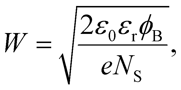 | (3) |
As a demonstration, in 2024, Wang and collaborators have developed the asymmetric 1T′-MoTe2/WS2/Au Schottky junctions for self-driven photodetection (Fig. 6a).142 As shown in Fig. 6b, compared to the conventional interface between 3D metals and 2D semiconductors severely degraded by Fermi level pinning, the 2D metal/2D semiconductor interface exhibits a much higher as-designed Schottky barrier. As shown in Fig. 6c and d, the asymmetric Schottky structure exhibits notable photocurrent at Vds = 0 V. The underlying working mechanism for the self-driven characteristics has been schematically depicted in Fig. 6e. On account of the severe Fermi level pinning effect, the built-in electric field at the WS2/Au interface is substantially smaller than the theoretical value. By contrast, taking advantage of the intact van der Waals interface, built-in electric field at the 1T′-MoTe2/WS2 junction is much stronger. As a consequence, the balance of the two electrode/channel interfaces is broken. Upon zero bias, photogenerated carriers are spontaneously separated, and a net photocurrent is generated due to the asymmetric interfacial built-in electric field. Overall, the use of 2D metals/semimetals as electrodes greatly enriches the available categories of Schottky junctions, providing a wide range of building blocks for constructing various types of high-performance self-driven 2DLM based Schottky junction photodetectors. Thus far, self-driven Gr/WSe2/Au,143 1T′-MoTe2/MoS2/Cr,144 Gr/WS2/Pt,145 1T′-MoTe2/InSe/Cr,146 Pd/GeSe/Gr,147 PtSe2/WSe2/Au,148 Gr/WSe2/Au,149 Cr/BP/WTe2,150 Gr/WSe2/Au,151 Sb2Te3/WSe2/Au,152 and Gr/WS2/Au153 photodetectors have been successfully demonstrated.
 | ||
| Fig. 6 (a) Schematic of a self-driven 1T′-MoTe2/WS2/Au photodetector. (b) Schematic diagrams of common 3D metal/semiconductor (left) and ideal 2D semimetal (metal)/semiconductor (right) Schottky structures (top panel) and the corresponding band structures (bottom panel). (c) J–V curves under dark (black line) and light illumination (red line). (d) Photocurrent as a function of light intensity. The inset summarizes the photoswitching curves. (e) Energy band diagram depicting the dynamic process of photocarriers at Vds = 0 V. Reproduced from ref. 142 with permission from John Wiley and Sons, Inc, copyright 2024. (f) Schematic illustration of a self-driven MSM-type WSe2 photodetector with graphene electrodes of different thicknesses. (g) I–V curves in darkness and under illuminations with various light intensities. (h) Photoswitching curve. Reproduced from ref. 155 with permission from American Chemical Society, copyright 2023. | ||
However, in practical applications, this strategy also has its own limitations. Specifically, the transfer process commonly involved in the fabrication of the heterogeneous electrode/channel van der Waals structures is prone to induce extrinsic contamination to the heterointerface, leading to a degradation in the contact quality. In addition, there generally exists a relatively large van der Waals gap at the heterogeneous interface of transferred van der Waals heterojunctions, which is also adverse to interfacial carrier transport. To resolve these issues, in 2023, by exploiting the thickness-dependent electronic band structure of 2DLMs, Zhang and collaborators developed a self-driven PdSe2 photodetector by exploiting conventional covalent metal contact and in situ integrated PdSe2 contact.154 Specifically, a thickness-uneven PdSe2 nanosheet is prepared by mechanical exfoliation and then transferred onto a substrate with pre-patterned Au electrodes. The Au pad contacting directly to the thin PdSe2 layer serves as one of the electrode. Since the thick PdSe2 layer is metallic, it serves as the other electrode for the thin PdSe2 channel, featuring damage-free, clean and seamless electrode/channel interface. Consequently, an asymmetric MSM-type photodetector has been successfully constructed. At zero bias, photocurrent mapping measurement reveals that opposite photocurrents appear at the contact region of the thin PdSe2/Au and the homojunction region between the thin and the thick PdSe2 nanoflakes, which conjointly contribute to the self-driven photoresponse. In addition, the device exhibits fast response speed. The response time and recovery time are as short as 0.24 and 0.72 ms, respectively. As a whole, this study exemplifies a straightforward approach for achieving high-performance and contamination-free self-driven 2DLM photodetectors by thickness engineering.
In addition, to further mitigate the detrimental interface effects, both electrodes can be replaced with 2D layered metals/semimetals. As an example, in 2023, Tong and collaborators prepared a self-driven Gr/WSe2/Gr photodetector based on asymmetric van der Waals contacts (Fig. 6f).155 Within this structure, graphene electrodes with different thicknesses have been exploited. Fig. 6g presents the I–V curve in darkness and under light illumination. The significant rectifying effect substantiates the formation of asymmetric interfacial barriers. In addition, the I–V curves detour the origin under illumination, demonstrating the occurrence of zero-bias photocurrent. Benefiting from the low dark current and highly efficient carrier collection, distinct on/off switching with the on/off ratio reaching ≈106 has been achieved (Fig. 6h). The underlying mechanism can be explained as follows. Since the electronic band structure of graphene is closely related with thickness, the employment of asymmetric graphene electrodes results in the difference in the interfacial built-in electric field. As a consequence, the balance of the two electrode/channel interface is broken, leading to the self-driven photoresponse. Most recently, Wang et al. reported on a zero-bias WS2 photodetector by using TaSe2 electrodes with different thicknesses.156 In addition to thickness tailoring, heteroatom doping is another approach to modulate the electronic structure of 2D electrodes. For a prototypical example, in 2022, Guo et al. developed a self-driven MoS2 photodetector by exploiting pristine graphene and N-doped graphene as electrodes.157 Under zero-bias voltage, the optimized responsivity and detectivity reach 0.63 A W−1 and 7.71 × 10¹² Jones, respectively. Moreover, the symmetry of the device can also be broken by using two distinct van der Waals semimetals/metals. Most recently, by integrating graphene and NbSe2 electrodes within a WSe2 photodetector, He et al. have achieved a self-driven photodetector with an ultra-high on/off ratio exceeding 105.158
It is worth noting that the above research works have mostly been based on the preparation of lateral MSM structures. However, there exist two potential shortcomings in terms of the structure of lateral MSM-type photodetectors. On one hand, the heterointerface of the lateral electrode/channel contact is substantially limited (i.e. quasi one-dimensional geometry in theory). This will lead to a substantially narrow depletion layer region, which is adverse to the spacial dissociation of photogenerated electron–hole pairs. On the other hand, due to the resolution limitation of micromachining processing technology, it is challenging to shorten the spacing between electrodes of the lateral devices (normally >2 μm for photolithography), which makes the transport path of photocarriers relatively long. This is adverse to the high-efficiency collection of photocarriers. Therefore, there is still an imperative demand to develop self-driven MSM-type photodetectors with vertical structures manifesting large contact area (i.e. 2D depletion layer), nanoscale transport path, etc. However, in terms of constructing vertical MSM structures, traditional electrodes have exhibited a host of shortcomings, including numerous surface dangling bonds, poor flatness, and low light transmittance. In recent years, a wealth of semi-metallic/metallic 2DLMs have been harnessed for use as electrodes, including graphene,159 1T′-WTe2,160 Bi2Te3,161 CoS2,162 PtTe2,163 PtBi2,164etc. These van der Waals materials typically have atomically flat surfaces, which are beneficial for suppressing notorious short-circuiting effect caused by surface undulations. In addition, the dangling-bond-free surface of 2DLMs can effectively suppress interfacial strain and defects, thereby reducing interfacial scattering and recombination of charge carriers. Furthermore, by taking advantage of the atomic-level thickness, these electrodes have relatively high light transmittance, allowing more incident light to pass through when used as top electrodes. By virtue of the above advantages, 2DLMs have indisputable potential for application in vertical self-driven MSM-type photodetectors.
As an example, in 2019, Wei et al. constructed asymmetric vertical Gr/MoTe2/Gr heterojunctions and successfully exploited them for self-driven photodetection (Fig. 7a).165 The asymmetry is mainly due to the distinct material properties enabled by different preparation methods. Specifically, p-type monolayer graphene layers grown by chemical vapor deposition (CVD) were used as the top contacts, n-type exfoliated multiple graphene layers were used as the bottom contacts, and exfoliated multilayer MoTe2 layers were used as the light-sensing channels. In dark, the Gr/MoTe2/Gr device exhibits distinct rectification effect, which is associated with the asymmetric interfacial barriers. Upon 1064 nm illumination, the I–V curve evidently bypasses the origin, indicative of the photovoltaic effect, which lays a solid foundation for self-driven photodetection. With the advantage of the atomic-scale transport path (i.e. the ultrathin thickness of the MoTe2 channel, ≈15 nm in this case), the vertical device exhibits a fast response rate with the rise/decay time down to 16.58/14.96 μs (Fig. 7b). Photovoltage mapping measurement reveals that the photovoltage is predominantly generated at the vertically overlapping region of the three flakes, which indicates that the photoresponse is originated from the heterointerface. Accordingly, the physical mechanism can be explained as follows. As shown in Fig. 7c, due to the difference in the Fermi levels of various components, built-in electric fields will be formed from n-type graphene to MoTe2 and from MoTe2 to p-type graphene after contact and equilibrium. Upon light excitation, photocarriers are generated, after which electrons will be driven to the n-type graphene and holes will be driven to the p-type graphene. As a consequence, a current flow from n-type graphene to p-type graphene is generated. Furthermore, it is further revealed that the thickness of the MoTe2 channel plays a critical role in the device properties. As shown in Fig. 7d, the photoresponse generally increases with increasing channel thickness. This is easily understandable since the light absorption enhances with increasing channel thickness. On the whole, the study has put forward a new scheme toward high-speed and high-sensitivity self-driven photodetection.
 | ||
| Fig. 7 (a) Schematic diagram of a vertical asymmetric Gr/MoTe2/Gr self-driven photodetector. (b) Temporal photoresponse. The red lines are the fitting curves. (c) Energy band diagrams of isolated (left) and contacted (right) n-type exfoliated graphene, p-type MoTe2, and p-type CVD-grown graphene. (d) Photocurrent as a function of light power intensity of Gr/MoTe2/Gr photodetectors with different MoTe2 channel thicknesses. The source–drain bias for (b) and (d) is zero. Reproduced from ref. 165 with permission from John Wiley and Sons, Inc, copyright 2019. | ||
6.2 Asymmetric contacts with distinct contact lengths
The integration of asymmetric electrodes with different work functions within one device has proven as an effective method for constructing MSM-type self-driven 2DLM photodetectors.128,131,141 In spite of the significant progress, this strategy has also come with its own formidable challenges. On one hand, a careful configuration of the work functions of the electrodes is required. On the other hand, due to the necessity to integrate two different types of metal electrodes, the fabrication process for preparing these asymmetric devices becomes exceptionally complex, requiring the deposition of the first kind of electrode, followed by the precise positioning and deposition of the second kind of electrode by using high-precision photolithography/electron-beam lithography technology. This significantly increases the complexity and technical difficulty of the preparation process, leading to a substantial decrease in practical device yield due to misalignment, thus restricting the feasibility in large-scale applications to some extent. In view of these insurmountable deficiencies, there is still an urgent need to explore and develop new device architectures to simplify the preparation process of self-driven 2DLM photodetectors, improving the yield and practicality.To this end, in 2018, Zhou et al. developed an MSM-type self-driven WSe2 photodetector with asymmetric metal contact geometries (Fig. 8a).76 Specially, compared to the common MSM-type devices with identical contact length at two ends (Fig. 8b), the contact lengths of the asymmetric device in the study are controlled to be discrepant (Fig. 8a). As shown in Fig. 8c, under illumination, the asymmetric WSe2 device demonstrates distinct photovoltaic characteristics, as evidenced by the I–V curves obviously bypassing the origin. In principle, the bias-free light-sensing characteristics can be explained as follows. Upon contact, a built-in electric field can be formed at the heterointerface of electrode and channel, on account of the different work functions of the two components. Under light illumination, photocurrent is generated under the drive of the built-in electric field. Of note, the photocurrent density of the two electrode/channel interface is identical since the interfacial potential is theoretically determined by the difference in the work functions of electrode and channel, while the directions are opposite due to the back-to-back configuration. As for the symmetric configuration (Fig. 8b), the photocurrent flows generated from the two heterogeneous interfaces are exactly compensated, and thus no photoresponse can be observed. As for the geometrically asymmetric configuration, the heterointerface with longer contact length dominates, and net photocurrent flow (ISC) can thus be generated according to
| ISC = JSC(WR − WL)t, | (4) |
 | ||
| Fig. 8 Schematic diagrams of the MSM-type photodetectors with (a) asymmetric contact geometry and (b) symmetric contact geometry. (c) I–V characteristic curves of the asymmetric device under illuminations with various light powers. The inset shows the measurement setup. (d) The open-circuit voltage (VOC) as a function of light power. (e) Light power dependent short-circuit current (ISC, black dots and line) and the corresponding zero-biased responsivity (red dots and line). (f) Contact length difference (ΔCL) dependent VOC. Reproduced from ref. 76 with permission from John Wiley and Sons, Inc, copyright 2018. | ||
6.3 Asymmetric contacts with different contact areas
In addition to the contact length of electrode, the interfacial area shared between the electrode and the light-sensing channel constitutes another crucial ingredient influencing the transfer of photoexcited charge carriers across the heterointerface, thereby opening up an additional promising pathway towards realizing self-driven optoelectronic sensing through technologically streamlined two-terminal architectures.As a demonstration, in 2023, Wang et al. transferred a rectangular Te nanosheet onto prepatterned Cr/Au electrodes with identical contact length but different contact areas at the two ends and demonstrated that the asymmetric device exhibited self-driven optoelectronic response.169 The structure of the device is schematically shown in Fig. 9a, where the contact area between the drain electrode and the Te channel is significantly smaller than that between the source electrode and the Te channel. As shown in Fig. 9b, under illumination, the Iph–Vd curves of the device evidently bypass the origin, which indicates a pronounced photovoltaic effect, providing a firm guarantee for self-driven optoelectronic sensing. Under a source–drain voltage of 0 V and periodic illumination, the device exhibits stable and reproducible on/off switching characteristics (Fig. 9c). By virtue of the extremely low dark current, the on/off ratio (Iph/Idark) under a self-driven mode is quite competitive, which is nearly three orders of magnitude higher than that under a biased operating mode (Fig. 9d). In addition, as the incident light power increases, the on/off ratio monotonically increases, due to the increased number of photoexcited carriers. Taking advantage of the suppressed shot noise, the detectivity under a self-driven mode reaches ≈1012 Jones, which is 1–2 orders of magnitude higher than that under biased conditions (Fig. 9e). In addition, the response/recovery time without bias is as short as 720 μs/1.16 ms (Fig. 9f). Fig. 9g shows the photocurrent mapping image. Evidently, the photocurrent is predominantly generated at the electrode/channel interfaces, and the directions of the photocurrent at the two ends are opposite. Of note, the photocurrent value in vicinity of the drain electrode is slightly higher than that in vicinity of the source electrode. Therefore, the physical mechanism of the self-driven characteristics of this asymmetric device can be explained as follows. Due to the lower Fermi level of Au as compared to Te, a built-in electric field pointing from Te towards Au will be formed after metallization. Under illumination, photoexcited electron–hole pairs are generated. Under the drive of the built-in electric field, photoelectrons near the source and drain electrodes drift towards the center of the Te channel. Due to the smaller contact area of the drain electrode as compared to the source electrode, there are fewer photoholes at the interface of the drain electrode, resulting in weaker attraction to photoelectrons and more efficient electron drift (Fig. 9h). Due to the discrepancy of electron drift at the two ends, zero-bias photoresponse is triggered. Overall, this study exemplifies a simple protocol free from complex microprocessing techniques for the implementation of self-driven 2DLM photodetectors via geometrical nonequivalence of source and drain contacts while using the same metal for electrodes. Most recently, Ghanbari et al. have prepared a self-driven MoSe2 photodetector based on an analogous scheme and achieved a remarkable responsivity of 4.38 × 10⁷ V W−1.170
 | ||
| Fig. 9 (a) Schematic diagram of a self-driven Te photodetector with electrodes of different contact areas. (b) Iph–Vd curves under 1550 nm illuminations with various light intensities. (c) Photoswitching curve under periodic 1550 nm illumination. (d) Iph/Idark and (e) detectivity as a function of light power under various biased conditions. (f) Temporal photoresponse. (g) Photocurrent mapping image without external bias. (h) Schematic illustration of the working mechanism for self-driven photoresponse. Reproduced from ref. 169 with permission from John Wiley and Sons, Inc, copyright 2023. | ||
7. Orthogonal electrodes
In addition to the material and geometry of electrodes, the modulation of the relative locations of electrodes is also an effective approach to reduce the overall symmetry of the device, providing a distinctive pathway for the implementation of self-driven photodetection. As a demonstration, in 2023, Semkin et al. fabricated a zero-bias photodetector with polarization discrimination capability by patterning metal contacts onto the orthogonal sides of a rectangular PdSe2 channel (Fig. 10a).171 As shown in Fig. 10b and c, the device exhibits pronounced polarization-dependent self-driven photoresponse. Specially, when the polarization of incident light is perpendicular to the source electrode, photocurrent predominantly generates at the source electrode/channel interface (left panel, Fig. 10b). By contrast, when the polarization of incident light is perpendicular to the drain electrode, photocurrent predominantly generates at the drain electrode/channel interface (right panel, Fig. 10b). To have an in-depth insight, systematic FDTD simulations have been performed. As shown in Fig. 10d, it is unveiled that the light field intensity is greatly enhanced at the electrode/channel interface when the polarization direction of incident light is perpendicular to the interface, which is associated with the lightning-rod effect.172 As for the proposed corner-type device, when one electrode is perpendicular to the polarization direction, the other one becomes parallel, which is thus selectively shadowed. As a consequence, the photocurrent flows generated at the two electrode/channel interfaces cannot be fully compensated, thus giving rise to self-driven photoresponse (Fig. 10a). On the whole, this study establishes a new scheme for realizing bias-free photodetection. Of note, since this strategy is independent of a particular material property, it is generic and can be theoretically applied to arbitrary 2DLMs in the upcoming future. | ||
| Fig. 10 (a) Schematic illustration of a self-driven PdSe2 photodetector with orthogonal metal contacts (corner-type device). (b) Photocurrent mapping images upon linearly polarized illuminations with polarization angles of 45° (perpendicular to the source electrode/channel interface) and −45° (perpendicular to the drain electrode/channel interface). (c) Photocurrent as a function of source–drain bias upon light illuminations with various polarization directions. (d) Electric field enhancement of corner-type (top panel) and slit-type (bottom panel) devices. Reproduced from ref. 171 with permission from American Chemical Society, copyright 2024. | ||
8. Asymmetric electrodes with discrepant thermal conductivities
Long-wave infrared (LWIR) photodetection has played a crucial role in remote sensing, infrared imaging, and other areas. Nonetheless, traditional 2DLM based LWIR photodetectors have been confronted with a series of dilemmas. In general, the photoconductive-type devices built of narrow-bandgap semiconductors/semimetals have suffered from large dark current, low signal-to-noise ratio, and high energy dissipation due to the numerous thermally excited free carriers. As a consequence, cryogenic cooling devices are generally required during operation to be competent for the standards of practical applications, which seriously increase device volume and operating cost. The photovoltaic devices, mostly built of p–n junctions or Schottky junctions, can address the above-mentioned predicaments by operating in a self-driven mode, where no source–drain bias is applied. However, there also exist some tricky challenges for this category of devices. For example, since the density of free carriers of narrow-bandgap semiconductors/semimetals is relatively high, the depletion layer therein of related heterojunctions is quite narrow. In addition, it is more challenging to form a staggered type-II band alignment, a favorable configuration to drive the segregation of photocarriers, due to the small interval of the conduction band minimum and valence band maximum of small-bandgap semiconductors. As a consequence, photoexcited electron–hole pairs easily recombine without being spacially separated, thus leading to poor photosensitivity. In addition, Fermi-level-pinning free heterointerface is required, which has been a long-standing bottleneck. Therefore, self-driven 2DLM LWIR photodetectors with new working mechanism have been the subject of intensive research.Photothermoelectric (PTE) detector is a distinctive type of device based on the Seebeck effect.173 Basically, the PTE effect is consisted of two pivotal processes: photothermal conversion and thermoelectric conversion. In the photothermal conversion process, carries absorb energy from photons, and then transfer the energy to the crystal lattice (i.e. thermal energy) through electron–phonon interactions. In the thermoelectric conversion process, the carriers are driven from the hot side to the cold side by the temperature gradient, leading to an electric potential difference (V) described by
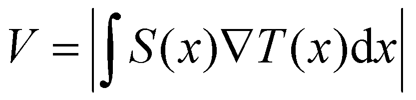 | (5) |
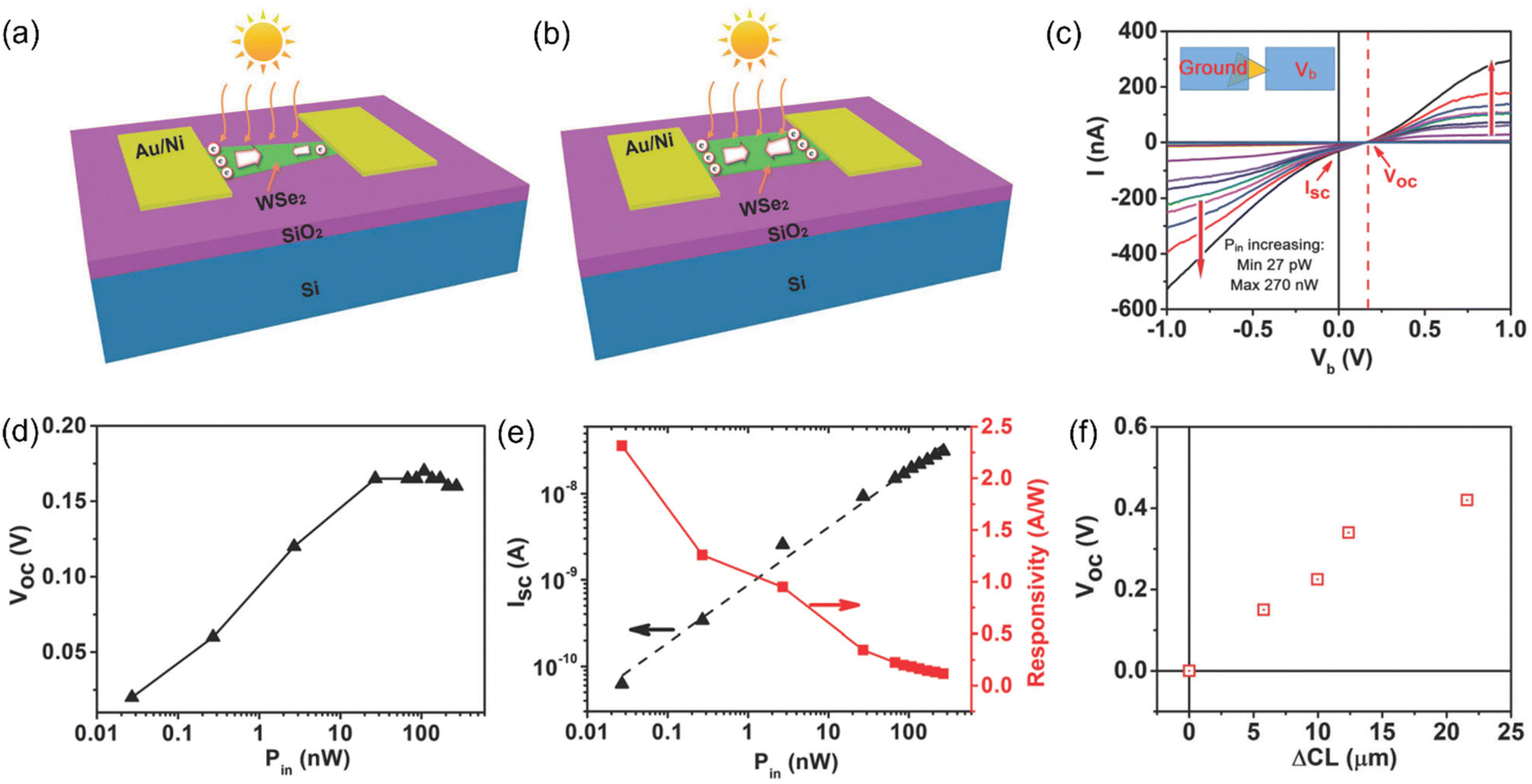
As an example, Dai et al. developed a PTE-type photodetector based on a semimetal PdSe2 nanoflake and successfully achieved self-driven LWIR photodetection through integrating asymmetric electrodes.178 The device structure of the MSM-type PdSe2 photodetector is schematically illustrated in Fig. 11a, where multilayer graphene (MLG) and Au electrodes are utilized as the electrically asymmetric contacts. As shown in Fig. 11b–d, under zero source–drain bias and room temperature, the MLG/PdSe2/Au device exhibits pronounced photoresponse to periodic 4.6, 7.4, and 10.5 μm global illuminations. The on/off switching is prompt, distinct, and well reversible, demonstrating great reliability. Of note, photovoltage mapping measurement has determined that the photoresponse is the most pronounced in vicinity of the electrode/channel interface (Fig. 11e). In addition, the photovoltage in vicinity of the Au electrode is evidently higher than that in vicinity of the MLG electrode, suggesting that the PTE effect of the former is stronger than that of the latter. In consideration of this, the self-driven photoresponse characteristics can be associated with the asymmetric PTE effects. Upon global illumination, the PdSe2 channel absorbs the photons and the temperature increases through photothermal conversion. Since the thermal conductivity of multilayer graphene (≈3000 W m−1 K−1) is substantially higher than that of Au (≈180 W m−1 K−1), the thermal dissipation of the former is much more efficient than that of the latter, thereby resulting in a lateral temperature gradient along the PdSe2 channel (Fig. 11f). As a consequence, photovoltage is generated due to the Seebeck effect. Moreover, by virtue of the anisotropic light absorbance enabled by the in-plane anisotropic crystal structure of 2D PdSe2, the self-driven MLG/PdSe2/Au photodetector has manifested pronounced polarized photoresponse, portending the prodigious potential for photodetection in complex environments and multifunctional optoelectronic applications (Fig. 11g–i). In general, this study unveils a facile and generic scheme, circumventing the necessity to realize Fermi-level-pinning-free heterointerface, toward self-driven LWIR 2DLM photodetectors by harnessing the Seebeck effect. It is noteworthy that despite the considerable disparity in the thermal conductivities of the two electrodes, Au also stands out as an exceptional heat sink, which hinders the establishment of a substantial temperature gradient between the two ends of the channel. Looking ahead, the conductors with low thermal conductivity (e.g., WxV1−xO2![[thin space (1/6-em)]](https://www.rsc.org/images/entities/char_2009.gif) 179) could be leveraged to substitute conventional metals, thereby amplifying the thermal conductivity contrast between the electrodes and consequently enhancing the photoresponse of the device even further.
179) could be leveraged to substitute conventional metals, thereby amplifying the thermal conductivity contrast between the electrodes and consequently enhancing the photoresponse of the device even further.
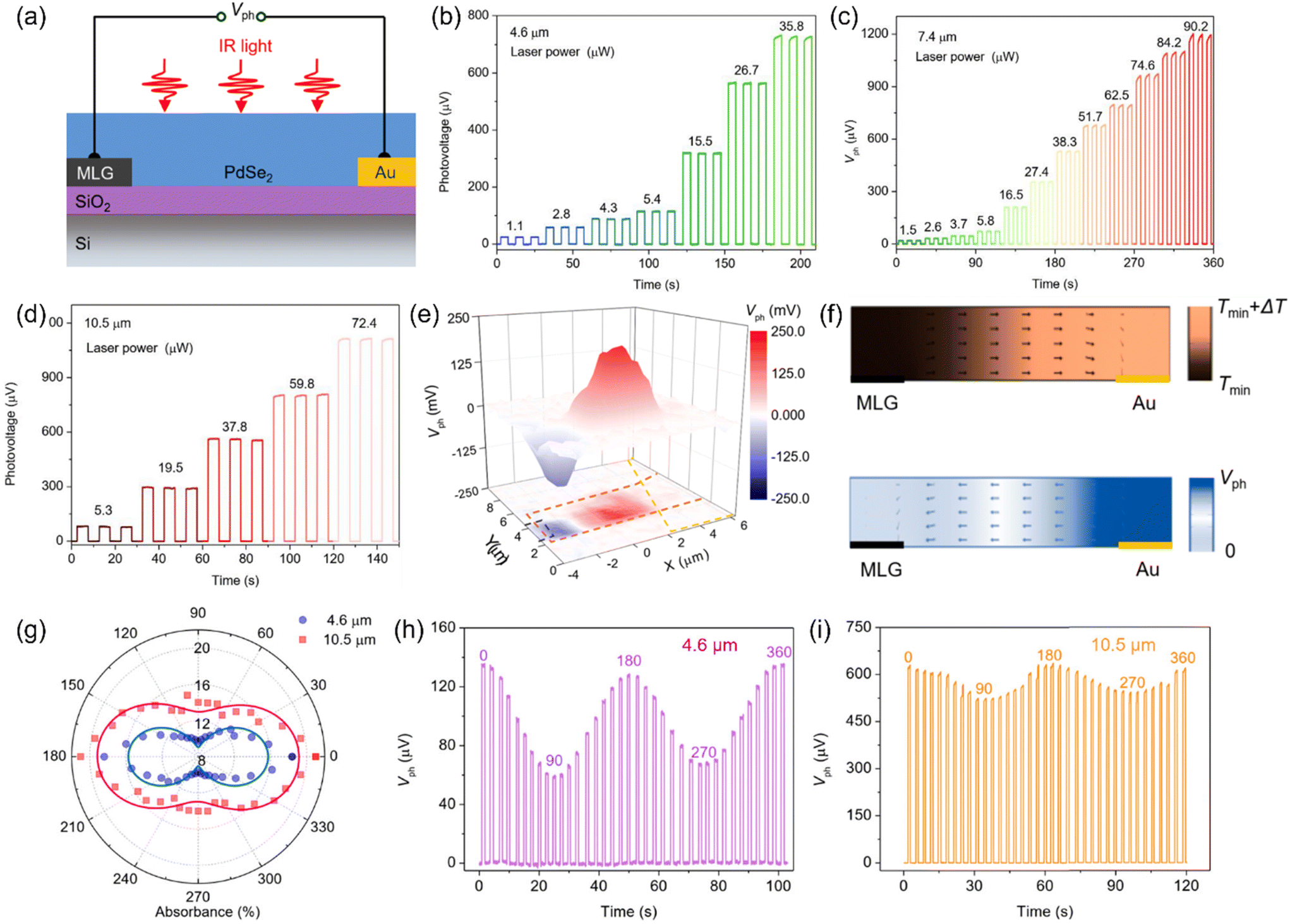 | ||
| Fig. 11 (a) Schematic diagram of an MSM-type PdSe2 photodetector with multilayer graphene (MLG) and Au as asymmetric electrodes. (b–d) Photoswitching curves under (b) 4.6 μm, (c) 7.4 μm, and (d) 10.5 μm periodic illuminations with different laser powers at zero bias. (e) 3D mapping plot of photovoltage (Vph) under 532 nm illumination. (f) Schematic diagrams of temperature (top panel) and photovoltage (bottom panel) distribution of the PdSe2 photodetector under global light illumination. The gradients of temperature and electric field are indicated by the black and blue arrows, respectively. (g) Polar plots of light absorbance as a function of the polarization angle of PdSe2 for 4.6 (blue line and circles) and 10.5 μm (red line and squares) incident light. (h–i) Polarized photovoltage response under (h) 4.6 μm and (i) 10.5 μm illuminations. Reproduced from ref. 178 with permission from American Chemical Society, copyright 2022. | ||
In addition to integrating asymmetric electrodes with different thermal conductivities to trigger a temperature difference, introducing a Seebeck coefficient gradient, through various ingredients such as contact doping effect enabled by electrodes with different work functions, is also a potential approach to achieve self-driven optoelectronic sensing.180 As a prototypical example, in 2020, Guo et al. demonstrated self-driven photodetection by depositing Cr/Au and Ti/Au electrodes at the two ends of a black phosphorus (BP) nanosheet (Fig. 12a).181Fig. 12b summarizes the photocurrent vs. source–drain voltage (Iph–V) curves of the black phosphorus photodetectors with symmetric and asymmetric electrodes under 0.12 Thz illumination. Evidently, under a source–drain bias of 0 V, the symmetric Cr/Au-BP-Cr/Au device exhibits negligible photoresponse, whereas the asymmetric Cr/Au-BP-Ti/Au device boasts distinct photocurrent, indicating that the asymmetric electrode configuration causes the self-driven photoelectric response. Under the irradiation of terahertz waves of different frequencies, the asymmetric black phosphorus device exhibits pronounced on/off switching characteristics (Fig. 12c). Specifically, upon 0.12 THz illumination, the rise time and decay time are as short as 0.8 and 1.5 μs, respectively (Fig. 12d). Overall, the self-driven optoelectronic characteristics of the Cr/Au-BP-Ti/Au device can be attributed to the symmetry breaking of Seebeck coefficient of the black phosphorus channel caused by different electrodes. As a rule, the Seebeck coefficient (S) of a material is closely related to the Fermi level (EF) and can be described by the following formula182
 | (6) |
 | ||
| Fig. 12 (a) Schematic illustration of a black phosphorus photodetector with asymmetric Cr/Au and Ti/Au contacts. (b) Iph–V curves of black phosphorus photodetectors with symmetric (blue line) and asymmetric (red line) contacts. (c) Photoswitching curves upon terahertz illuminations with different frequencies. (d) Temporal photoresponse. (e) Schematic illustration of the spacial distribution of temperature, Seebeck coefficient, and electric potential. (f) Polar plot of the photocurrent as a function of polarization angle. Reproduced from ref. 181 with permission from John Wiley and Sons, Inc, copyright 2020. | ||
In addition to electrodes, dielectric layers can also have a significant effect on the Seebeck coefficient of 2DLMs, providing another pathway for the implementation of self-driven 2DLM photodetectors. For a prototypical example, in 2023, Razeghi et al. achieved a single material MoS2 thermoelectric junction by substrate engineering by locating a MoS2 nanosheet onto a holey substrate.184 It turns out that the self-driven photoresponse can be generated in a supported MoS2/suspended MoS2 homojunction. This can be explained by the difference in Seebeck coefficient on account of the variation in the dielectric environment, which alters both the electron–phonon scattering mechanism and the Fermi level of MoS2.
9. Ferroelectricity-enabled bulk photovoltaic effect
As previously elaborated, the upper limit of photovoltaic output achievable by traditional p–n junctions is dictated by the renowned Shockley–Queisser theory, posing a formidable barrier to advancing the device properties. Consequently, it becomes imperative to embark on exploring novel strategies aimed at attaining self-driven operation. Ferroelectric materials are unique substances characterized by spontaneous polarization, which can be readily adjusted by an external electric field. Typically, these materials exhibit low-symmetry crystalline structures in which the centers of positive and negative charges fail to overlap. This inherent structural asymmetry engenders the emergence of an internal electric field, oriented in opposition to the direction of the ferroelectric polarization. Since the ferroelectric polarization is nonvolatile, the resulting internal electric field can be exploited as the impetus to drive the spacial separation of photocarriers, a process recognized as the BPVE. In this consideration, ferroelectricity opens up new possibilities for realizing bias-free 2DLM photodetectors.As proof of the potency, in 2024, Li et al. constructed a self-driven 2DLM photodetector by exploiting the ferroelectricity-enabled BPVE, in which a Sn2P2S6 nanosheet is sandwiched vertically between two thin graphene layers, as schematically shown in Fig. 13a and b.185 As presented in Fig. 13c, the poled Sn2P2S6 device exhibits stable photoresponse to periodic light simulations. In addition, the direction of the photocurrent can be flexibly switched by inversing the ferroelectric polarization direction, confirming the ferroelectricity origin of the self-driven optoelectronic characteristics. Essentially, the ferroelectric polarization inherent in the vertically poled Sn2P2S6 nanosheet establishes a robust built-in electric field extending along the out-of-plane axis. Upon illumination, photogenerated electrons and holes within the Sn2P2S6 matrix are efficiently segregated along opposite trajectories, thereby spontaneously triggering a photoresponse without the need for external biasing. Furthermore, taking advantage of the polarization-sensitive light absorption (Fig. 13d), the Sn2P2S6 photodetector exhibits distinct polarized photosensitivity (Fig. 13e). Specifically, by using the Sn2P2S6 device as the sensing component, polarization-sensitive imaging has been realized (Fig. 13f). Broadly speaking, this study presents a straightforward pathway that sidesteps the intricate methodologies typically required for crafting high-quality p–n junctions, Schottky barriers, and homojunctions, thereby facilitating the realization of self-driven 2DLM photodetectors in a more accessible manner. Thus far, a series of ferroelectric 2DLMs, including CuInP2S6,186 SnS,187,188 ReS2,189 SnP2Se6,190 and α-In2Se3,191,192 have been successfully harnessed for self-driven photodetection by exploiting the similar mechanism.
 | ||
| Fig. 13 (a) Schematic diagram of a vertical Gr/Sn2P2S6/Gr photodetector. (b) A typical optical microscopy image. The inset shows the AFM topography image and the height profiles. (c) Photoswitching curves at zero bias under different poled states. (d) Contour mapping of the polarized light absorption of Sn2P2S6. (e) Polar plots of the photoresponse as a function of polarization angle under illuminations with various light powers. (f) The imaging results with the polarization angles of 0° (left panel) and 90° (right panel). Reproduced from ref. 185 with permission from American Chemical Society, copyright 2024. | ||
As aforementioned, self-driven 2DLM photodetectors, which harness BPVE as the underlying operating mechanism, commonly necessitate the employment of channel materials that possess intrinsic ferroelectricity. Nevertheless, a substantial portion of 2DLMs, notably the widely explored transition metal dichalcogenides, possess relatively high crystalline symmetry, which inherently limits the manifestation of ferroelectric properties. Fortunately, by meticulously manipulating the growth direction, it is feasible to degrade the overall symmetry of 2DLMs, thereby unleashing the potential for ferroelectric behavior as well as BPVE devices.
In their most recent endeavor, Xue and colleagues successfully accomplished the oriented growth of WS2via an atomic manufacturing strategy (Fig. 14a), yielding diverse nanostructures such as zigzag, armchair, and chiral ribbons.193 Remarkably, the armchair-structured WS2 photodetector demonstrates a pronounced self-driven photoelectric response, evidenced by the I–V curves obviously detouring the origin upon illumination (Fig. 14b). Furthermore, the device displays a noteworthy polarization photosensitivity, with the photocurrent manifesting a periodic variation as the polarization angle varies from 0 to 360° (Fig. 14c). Notably, the photocurrent attains the maximum value when the polarization direction aligns parallel to the growth orientation, whereas it diminishes to the nadir when the polarization direction is perpendicular to the growth axis. Further investigations have unveiled that the photoresponse of the armchair WS2 photodetectors is much higher than those of the chiral and zigzag devices (Fig. 14d). This compelling finding suggests that the self-driven photoresponse characteristics of the armchair devices stem from the ferroelectricity induced by the degraded symmetry. When WS2 grows along the armchair direction, the equivalent negative charge center formed by S atoms fail to overlap with the equivalent positive charge center formed by W atoms. Therefore, an internal electric field is generated (Fig. 14e). After photoexcitation of electron–hole pairs, the electrons and holes migrate in the opposite directions under the drive of the internal electric field, resulting in the generation of photocurrent. In summary, this pioneering research introduces a novel perspective for the realization of self-driven photodetectors, which heralds the potential for extensive application to additional 2DLMs, including MoS2, MoSe2, and WSe2, in the imminent future.
 | ||
| Fig. 14 (a) Schematic illustration for the oriented growth of WS2. (b) I–V curves in darkness and under illuminations with various light power intensities. (c) Photocurrent as a function of polarization angle. The inset showcases the schematic definition of the polarization angle. (d) Photocurrent values of the armchair (AC-R), chiral (C-R), and zigzag (ZZ-R) WS2 photodetectors. (e) Schematic comparison of the polarization states of armchair and zigzag WS2. Reproduced from ref. 193 with permission from American Association for the Advancement of Science, copyright 2024. | ||
10. Self-driven photodetectors enabled by asymmetric optical antennas
As mentioned above, provided 2DLMs boast intrinsic ferroelectricity, the non-volatile polarization induced electric field can spontaneously drive photocarriers and lead to the formation of bulk photovoltaic effect (BPVE), thereby enabling self-driven photodetection. However, in reality, most 2DLMs, such as graphene and MoS2, have negligible intrinsic ferroelectricity. In this consideration, the strategy of ferroelectric engineering for self-driven photoelectric sensing suffers from relatively poor universality. In response to this predicament, it is thus necessary to explore an alternative strategy devoid of ferroelectricity to achieve self-driven photodetection by exploiting the bulk photovoltaic effect.As an example, in 2020, Wei et al. demonstrated self-driven photoelectric detection by integrating non-centrosymmetric plasmonic optical antennas onto a graphene channel.194 The structure of the device is schematically shown in Fig. 15a. A metasurface, which is consisted of periodic subwavelength and non-centrosymmetrical T-shaped Au patterns, has been prepared on a graphene channel by using standard electron beam lithography technique. Fig. 15b summarizes the output curves in darkness and under various illuminations. Specifically, compared to the I–V curve in the darkness, the curves under illuminations manifest a significant parallel shift, indicating that the non-centrosymmetric device possesses self-driven photoelectric response. In addition, under polarized light irradiation with polarization angles of 0 and 90 degrees, the skewing directions of the I–V curves are opposite, indicating that the device possess polarization sensitivity. Under periodic illumination, the device exhibits fast, stable, and reproducible photoresponse (Fig. 15c). Its response/recovery time is as short as ≈100/100 μs. Finite-different time-domain (FDTD) simulations determine that the self-driven photoresponse of the device is mainly due to the non-uniformity of the light field intensity, induced by the non-centrosymmetric T-shaped plasmonic optical antennas (Fig. 15d). As a consequence, directional net photocarriers are generated, leading to the generation of photocurrent. Similarly, in another following study, by modifying a graphene channel with double L-shaped nanoantennas, Xie et al. demonstrated high-performance long-wave infrared zero-biased photodetection with a high responsivity of 6.3 V W−1 and a low noise-equivalent power of 1.6 nW Hz−1/2.195 Most recently, Koepfli and colleagues showcased a graphene-based photodetector that exhibited remarkable performance characteristics, including a high responsivity of 1.5 V W−1 and an impressive operational frequency exceeding 400 GHz, achieved through the coupling of a “T”-shaped metamaterial perfect absorber architecture.196 Overall, these studies have provided a new strategy for self-driven photodetection through the bulk photovoltaic effect unconstrained by specific family of materials.
 | ||
| Fig. 15 (a) Schematic diagram of a self-driven graphene photodetector enabled by non-centrosymmetrical T-shaped plasmonic optical antennas. (b) I–V curves in darkness (dark line) and under light illuminations with various polarization directions (red & purple lines). Polarization angle: the angle between the direction of polarized light and the direction of source–drain bias. 0°: red line. 90°: purple line. (c) Photoswitching curve under periodic illumination at a source–drain bias of 0 V. (d) Simulated spacial distribution of the light field intensity upon light excitation with various polarization directions (indicated by the double-headed arrows). Yellow wave arrow: flow of photocarriers. White arrow: the resultant vectorial photocurrent. Reproduced from ref. 194 with permission from Nature Publishing Group, copyright 2020. | ||
In addition to integrating non-mirror-symmetric optical antennas within the 2DLM photosensitive channels, constructing electrodes with different light-harvesting capabilities is also an alternative protocol for achieving self-driven photodetection. As an example, most recently, Zhang et al. designed asymmetric bowtie split ring (BSR) and common rectangular electrodes on the two ends of a graphene channel (Fig. 16a), and achieved self-driven photodetection based on this non-centrosymmetrical device.197 The I–V curves of the device under different conditions have been summarized in Fig. 16b. Apparently, compared to the I–V curve in darkness, the I–V curve under illumination shows a significant parallel shift away from the origin, indicating self-driven photoresponse characteristics. Specifically, the optimal responsivity reaches 138 V W−1 (Fig. 16c), and the optimal noise equivalent power (NEP) is as low as 25 pW Hz−1/2 (Fig. 16d). The self-driven photoresponse of the asymmetric graphene device is mainly emanated from the localized light field enhancement effect enabled by the BSR electrode. As shown in Fig. 16e, profited from the inductor–capacitor and dipole resonances, the light field intensity on the BSR electrode side is significantly enhanced. Therefore, the corresponding light absorption is much stronger as compared to the other end. As a result, a temperature gradient is generated between the two ends, causing the self-driven photothermoelectric response via Seebeck effect (bottom panel of Fig. 16a). Most recently, Zhang et al. have achieved self-driven polarization-sensitive photodetection by integrating stripe- and triangle-shaped electrodes on the two ends of a graphene channel.198 On the whole, the findings presented herein herald optical engineering as a promising scheme to enable self-driven photodetection. As is universally acknowledged, the resonance characteristics of plasmonic optical structures are intricately tied to a multitude of ingredients encompassing shape, scale, and periodicity.199 In the future, further refining optical antennas ought to be undertaken with the assist of numerical simulations, aiming to more precisely align them with the incident light and attain optimal light harvesting.
 | ||
| Fig. 16 (a) Schematic diagram of a self-driven graphene photodetector with asymmetric electrodes (top panel). The spacial distributions of temperature, Seebeck coefficient and electric potential have been summarized in the bottom panel. (b) I–V curves in darkness (dark line) and under 84 GHz light illumination (orange line). (c) Responsivity and (d) NEP as a function of the frequency of incident light. (e) Field enhancement as a function of frequency of dipole (blue line) and BSR (pink line) resonances. Reproduced from ref. 197 with permission from American Chemical Society, copyright 2022. | ||
11. Self-driven photodetectors enabled by asymmetric carrier scattering
As previously noted, the realization of self-driven photodetectors inherently necessitates harnessing the built-in electric fields to segregate photogenerated electron–hole pairs. Nevertheless, the establishment of built-in electric field commonly entails the intricate design of heterojunctions or homojunctions, which have been frequently plagued by serious interface challenges (contaminations, deformations, etc.). Most notably, the fabrication of these structures involves costly, complex, and labor-intensive processes, thereby impeding their widespread adoption. Consequently, researchers have been relentlessly pursuing innovative approaches to develop interfacial built-in electric field-free self-driven 2DLM optoelectronic devices to overcome these limitations.As a prototypical example, in 2020, Guo et al. achieved bias-free terahertz detection based on anisotropic carrier scattering of 2D PdTe2.200Fig. 17a shows the structure diagram of the device. An MSM-type configuration is exploited, with a PdTe2 nanosheet as the photosensitive channel and Cr/Au pads as the electrodes. As shown in Fig. 17b, the device exhibits stable response to terahertz light at a source–drain voltage of 0 V. By virtue of the excellent air-stability of PdTe2, the photoresponse remains largely invariable after one month of storage. In addition, the device exhibits a fast response rate, with a response/recovery time as short as 1/2.2 μs (Fig. 17c). As shown in Fig. 17d, the photocurrent is almost linearly related to the incident light power density, and the corresponding responsivity reaches ≈0.2–0.3 A W−1. In general, the self-driven photoresponse of the device is mainly originated from asymmetric carrier scattering. As schematically shown in “i” of Fig. 17e, in darkness, the disordered movement of charge carriers causes scattered charge carriers in all directions to compensate each other, resulting in a negligible net current. Under polarized terahertz illumination, charge carriers move back and forth along the polarization direction, under the drive of the ac electric field. Since PdTe2 boasts a C3v symmetry point group, the carrier elastic scattering can be deem as scattering by randomly distributed wedges with consistent orientation, and the scattering is highly anisotropic. Specifically, a polarization parallel to the base of the wedges yields the net electron flow perpendicular to the base, along the normal direction (ii, Fig. 17e). By contrast, a polarization perpendicular to the base of the wedges yields the net electron flow in an opposite direction (iii, Fig. 17e). As a consequence, self-driven photoresponse can be achieved, manifesting pronounced polarization sensitivity. Capitalizing on an analogous working mechanism, self-driven detectors have been implemented by using a series of 2DLMs, including Bi2Se3,201 Sb2Te3,202 and MnBi2Te4,203 substantiating the extensive applicability and versatility of this innovative strategy.
 | ||
| Fig. 17 (a) Schematic diagram of an MSM-type PdTe2 terahertz detector. (b) Photoswitching curves under zero bias of a PdTe2 device right after fabrication (blue line) and after storage in air for one month (orange line). (c) Temporal photoresponse. (d) Photocurrent (black line and triangulars) and responsivity (red line and circles) as a function of light power density. (e) Schematic illustration of the working mechanism for the self-driven photoresponse. Reproduced from ref. 200 with permission from American Association for the Advancement of Science, copyright 2020. | ||
12. Conclusion & perspectives
A systematic overview on the new paradigms of self-driven photodetectors built of 2DLMs has been provided. Firstly, the emerging strategies for implementing various self-driven 2DLM photodetectors have been epitomized, including strain modulation, thickness tailoring, structural engineering, asymmetric ferroelectric gating, asymmetric contacts (including work function, contact length, and contact area), ferroelectricity-enabled bulk photovoltaic effect, asymmetric optical antennas, etc., with the focus on the fundamental physical principles of the self-driven characteristics. For clarity, Table 1 has summarized the pivotal figures-of-merit of the emerging self-driven 2DLM photodetectors. Following the above summarization, the ongoing challenges in this research field have been identified, and potential solutions addressing them have been proposed. On the whole, this review depicts a comprehensive blueprint for the implementation of self-driven, high-performance, and highly integrated 2DLM optoelectronic devices, which marks the advent of a new era of 2D optoelectronics. Nevertheless, despite the rapid development, the research regarding new paradigms of 2DLMs based self-driven photodetectors is in its nascent stage, and there are still a host of issues that urgently need to be addressed.| Device | R (A W−1) | EQE (%) | D* (Jones) | τ rise/τdecay | Ref. |
|---|---|---|---|---|---|
| a N. A.: not applicable. b BP: black phosphorus. c Gr: graphene. d N-Gr: N doped graphene. e The output signal is recorded in the form of voltage. f BSR: bowtie split ring. | |||||
| Thin-MoTe2/thick-MoTe2 | 0.63 | N. A.a | 1.38 × 10⁹ | 15 ms/17 ms | 78 |
| Thin-WSe2/thick-WSe2 | 0.0112 | 2.6 | 4.4 × 10¹⁰ | 0.18 ms/0.22 ms | 107 |
| Rolled WSe2/flat WSe2 | 0.0346 | N. A. | 3.24 × 10⁹ | 23.1 ms/16.8 ms | 117 |
| Ferroelectricity-enabled MoTe2 homojunction | 1.5 | 3 | N. A. | N. A. | 120 |
| Ferroelectricity-enabled MoTe2 homojunction | 5 | 40 | 3 × 10¹² | 30 μs | 121 |
| Ferroelectricity-enabled MoS2 homojunction | 0.015 | N. A. | N. A. | 20 μs | 122 |
| Ferroelectricity-enabled BP homojunctionb | 1.06 | 90.8 | 1.27 × 10¹¹ | 361 μs/362 μs | 124 |
| Ferroelectricity-enabled MoTe2 homojunction | 0.22 | 41 | N. A. | N. A. | 125 |
| Au/InSe/In | 0.369 | ≈100 | N. A. | 23 ms/25 ms | 131 |
| Au/MoS2/Ag | 0.07564 | 15 | 1.27 × 10¹² | 8.85 ms/0.96 ms | 133 |
| Mo2C/MoS2/Au | 10−4 | N. A. | N. A. | 23 s/28 s | 135 |
| Cr/GeSe/Pdc | 0.28 | N. A. | 4.1 × 10⁹ | 69 ms/92 ms | 147 |
| MoO2/MoSe2/Ag | 9.79 × 10⁻³ | 2.3 | 6.23 × 10⁹ | 5 ms/6 ms | 137 |
| 1T′-MoTe2/MoS2/Cr | 0.088 | 20 | N. A. | N. A. | 144 |
| 1T′-MoTe2/InSe/Cr | 0.048 | N. A. | 1.6 × 10¹² | 29 ms/29 ms | 146 |
| PtSe2/WSe2/Au | 0.316 | 61.8 | 2.1 × 10¹¹ | 830 μs/950 μs | 148 |
| Cr/BP/WTe2 | 0.283 | 67 | 2.3 × 10¹¹ | N. A. | 150 |
| Au/WSe2/Gr | 0.286 | 98 | 2.6 × 10¹² | 48 ms/45 ms | 151 |
| Thick-PdSe2/thin-PdSe2/Au | 0.053 | N. A. | 5.17 × 10¹¹ | 0.72 ms/0.24 ms | 154 |
| Thick-Gr/WSe2/Thin-Gr | 0.02031 | 4 | 4.48 × 10⁹ | 42.9 μs/56.0 μs | 155 |
| Thick-TaSe2/WS2/Thin-TaSe2 | 0.292 | 57 | 2.43 × 10¹¹ | 43 μs/54 μs | 156 |
| Gr/WSe2/NbSe2 | 0.287 | 88 | 5.3 × 10¹¹ | 80 μs/72 μs | 158 |
| Gr/MoS2/N-Grd | 0.63 | 138 | 7.71 × 10¹² | 26 μs/50 μs | 157 |
| InSe with different contact lengths | 0.103 | 24.5 | 1.83 × 10¹⁰ | 1 ms/2.3 ms | 167 |
| ReSe2 with different contact lengths | 0.379 | 63.49 | 6.8 × 10¹¹ | 18.8 ms/21.6 ms | 168 |
| Te with different contact areas | 26.1 | 2090.9 | 3.24 × 10⁹ | 720 μs/1.16 ms | 169 |
| Gr/PdSe2/Au | 21.6 V W−1e |
N. A. | 6.7 × 10⁶ | 42.7 μs/51.9 μs | 178 |
| Cr/BP/Au | ≈185 V W−1 | N. A. | N. A. | 0.8 μs/1.5 μs | 181 |
| Gr/Sn2S2P6/Gr | 3 × 10⁻³ | 0.8 | 5 × 10⁹ | 0.23 s/0.19 s | 185 |
| Gr/ReS2/Gr | 0.11 | 25.7 | N. A. | 70.2 μs/79.4 μs | 189 |
| Gr/α-In2Se3/Gr | 0.035 | 8.5 | N. A. | N. A. | 191 |
| Gr/α-In2Se3/Gr | 1.8 × 10⁻³ | N. A. | N. A. | N. A. | 192 |
| Graphene modified with T-shaped antennas | 0.0363 | 1.1 | 5 × 10⁶ | ≈100 μs | 194 |
| Graphene modified with L-shaped antennas | 6.3 V W−1 | N. A. | N. A. | 1 μs | 195 |
| Graphene modified with T-shaped antennas | ≈1.5 V W−1 | N. A. | N. A. | N. A. | 196 |
| BSR electrode/Gr/rectangle electrodef | 138 V W−1 | N. A. | N. A. | 3.7 μs | 197 |
| Graphene with stripe- and triangle-electrodes | 0.025 | N. A. | N. A. | 0.2 ms/0.2 ms | 198 |
| PdTe2 | ≈0.28 | N. A. | N. A. | 1 μs/2.2 μs | 200 |
| Bi2Se3 | 75 | N. A. | N. A. | 66 μs/68 μs | 201 |
| Sb2Te3 | 0.0385 | 27.3 | 3.44 × 10¹⁰ | 26 μs/20 μs | 202 |
(a) Overall, the photosensitivity of the self-driven 2DLM photodetectors based on the new paradigms is still comparatively modest in the current stage. Therefore, elevating device efficiency is pressing task. It is well recognized that this limitation stems predominantly from two disadvantageous ingredients. On one hand, the inherent thinness of 2DLMs significantly curtails the light absorption cross-section, resulting in a substantially limited light absorption cross-section and thereby low absorbance. On the other hand, the separation efficiency of photocarriers is relatively low because the device structures have been far from optimized. In the future, the light–2DLM interactions can be enhanced through strategies such as modifying optical antennas and integrating optical cavities/waveguides. In addition, the impetus for segregating photogenerated electron–hole pairs can be augmented through the simultaneous exertion of multiple strategies (e.g. asymmetric contact and thickness tailoring), thereby achieving an improvement in the photoelectric conversion efficiency by leveraging the collaborative effects.
(b) Even though a series of ingenious approaches have been harnessed for self-driven photodetection based on 2DLMs, these strategies, while effective, generally exhibit their own sets of limitations that make them difficult to fully meet the escalating demands for optoelectronic applications necessitating various 2DLMs. For example, self-driven MSM-type photodetectors based on asymmetric electrodes with distinct work functions are in need of the formation of ideal Schottky contacts between the metals and light-sensing channel, which is quite challenging for a variety of 2DLMs due to the complex interfacial effects such as the Fermi level pinning.144,204 In addition, self-driven photodetectors based on ferroelectricity-enabled bulk photovoltaic effects entail 2DLMs with low-symmetry crystal structures, which hinders its application in high-symmetry 2DLMs with more mature synthesis process (e.g., MoS2, WS2). Furthermore, structural engineering (e.g. rolling 2DLMs) requires extremely complex and cumbersome fabrication processes, which can hardly be scalable. In this consideration, it is thus still imperative to develop self-driven 2DLM photodetectors with exceptional working principles. From the preceding advancements, it can be determined that the implementation of self-driven photodetection fundamentally relies on the breaking of symmetry of devices. In addition to thickness and strain, the dielectric environment is also an important parameter affecting the electronic band structure of 2DLMs.47,205,206 In this consideration, self-driven photodetection can be theoretically achieved through dielectric contrast engineering. Furthermore, apart from the asymmetry of electronic band structure and electrode, the asymmetry of the light field can also induce self-driven photoresponse by localized heating.174,175 Asymmetric light field distribution can be achieved through selective-area modification of plasmonic optical antennas, leading to the development of a new paradigm for self-driven 2DLM photodetectors. By exploiting electrodes of different thicknesses to generate transmittance contrast, another alternative strategy is afforded for achieving heterogeneous heating.207 In the future, more enthusiasm should be devoted to developing new-paradigm self-driven 2DLM photodetectors.
(c) The large-scale fabrication of ordered arrays of devices stands as a pivotal prerequisite indispensable for the practical exploitation of novel materials in real-world applications. To date, the overwhelming majority of self-driven photodetectors leveraging 2DLMs have been produced through intricate micromechanical exfoliation and transfer methodologies.208 However, these techniques are stalled by inherent limitations in controllability and productivity, coupled with the necessity for cumbersome procedures. Consequently, the quest for scalable preparation of 2DLM-based devices has persisted as a longstanding dilemma. Inspiringly, some pioneering studies have consolidated that synthesis techniques such as interface epitaxy,209 chemical vapor deposition,210–213 metal–organic chemical vapor deposition,214–216 molecular beam epitaxy,213,217,218 pulsed-laser deposition,64,219 roll printing,220 atomic layer deposition,221 and magnetron sputtering222,223 boast the potential for scalable preparation. In the future, research endeavors should be focused on refining these large-area growth methodologies and exploring non-destructive patterning techniques, with the aim of preparing diverse 2DLMs in a scalable and efficient manner.
As a concluding remark, there exist a myriad of burgeoning device engineering schemes for the implementation of self-driven photodetection based on 2DLMs. These devices have provided a wide range of avenues for promoting next-generation optoelectronic devices characterized by unparalleled signal-to-noise ratio, low energy consumption, and exceptional integration capabilities, which will catalyze transformative strides in device paradigms. Looking ahead, with further improvements in device performance, the new paradigms of self-driven 2DLM photodetectors are set to shed light on the next era of the optoelectronic industry.
Data availability
No primary research results, software or code have been included and no new data were generated or analysed as part of this review.Conflicts of interest
The authors declare no competing interests.Acknowledgements
This work is supported by the National Natural Science Foundation of China (Grant No. 52272175, U2001215), the Natural Science Foundation of Guangdong Province (Grant No. 2022A1515011487, 2021A1515110403), and State Key Laboratory of Optoelectronic Materials and Technologies (Sun Yat-sen University).References
- K. S. Novoselov, A. K. Geim, S. V. Morozov, D. Jiang, Y. Zhang, S. V. Dubonos, I. V. Grigorieva and A. A. Firsov, Science, 2004, 306, 666–669 CrossRef CAS PubMed
.
- J. D. Yao, Z. Q. Zheng and G. W. Yang, Prog. Mater. Sci., 2019, 106, 100573 CrossRef CAS
- A. Chaves, J. G. Azadani, H. Alsalman, D. R. da Costa, R. Frisenda, A. J. Chaves, S. H. Song, Y. D. Kim, D. He, J. Zhou, A. Castellanos-Gomez, F. M. Peeters, Z. Liu, C. L. Hinkle, S. H. Oh, P. D. Ye, S. J. Koester, Y. H. Lee, P. Avouris, X. Wang and T. Low, npj 2D Mater. Appl., 2020, 4, 29 CrossRef CAS
- J. Yao and G. Yang, Nanoscale, 2020, 12, 454–476 RSC
- Q. Fu, J. Han, X. Wang, P. Xu, T. Yao, J. Zhong, W. Zhong, S. Liu, T. Gao, Z. Zhang, L. Xu and B. Song, Adv. Mater., 2021, 33, 1907818 CrossRef CAS PubMed
- J. Yao and G. Yang, Nanotechnology, 2021, 32, 392001 CrossRef CAS PubMed
- S. Das, A. Sebastian, E. Pop, C. J. McClellan, A. D. Franklin, T. Grasser, T. Knobloch, Y. Illarionov, A. V. Penumatcha, J. Appenzeller, Z. Chen, W. Zhu, I. Asselberghs, L.-J. Li, U. E. Avci, N. Bhat, T. D. Anthopoulos and R. Singh, Nat. Electron., 2021, 4, 786–799 CrossRef CAS
- J. F. Sierra, J. Fabian, R. K. Kawakami, S. Roche and S. O. Valenzuela, Nat. Nanotechnol., 2021, 16, 856–868 CrossRef CAS PubMed
- P. Ares and K. S. Novoselov, Nano Mater. Sci., 2022, 4, 3–9 CrossRef CAS
- Q. H. Wang, A. Bedoya-Pinto, M. Blei, A. H. Dismukes, A. Hamo, S. Jenkins, M. Koperski, Y. Liu, Q. C. Sun, E. J. Telford, H. H. Kim, M. Augustin, U. Vool, J. X. Yin, L. H. Li, A. Falin, C. R. Dean, F. Casanova, R. F. L. Evans, M. Chshiev, A. Mishchenko, C. Petrovic, R. He, L. Zhao, A. W. Tsen, B. D. Gerardot, M. Brotons-Gisbert, Z. Guguchia, X. Roy, S. Tongay, Z. Wang, M. Z. Hasan, J. Wrachtrup, A. Yacoby, A. Fert, S. Parkin, K. S. Novoselov, P. Dai, L. Balicas and E. J. G. Santos, ACS Nano, 2022, 16, 6960–7079 CrossRef CAS PubMed
- J. Qi, Z. Wu, W. Wang, K. Bao, L. Wang, J. Wu, C. Ke, Y. Xu and Q. He, Int. J. Extreme Manuf., 2023, 5, 022007 CrossRef CAS
- S. Song, M. Rahaman and D. Jariwala, ACS Nano, 2024, 18, 10955–10978 CrossRef CAS PubMed
- Z. Huang, Y. Li, Y. Zhang, J. Chen, J. He and J. Jiang, Int. J. Extreme Manuf., 2024, 6, 032003 CrossRef
- R. Wu, H. Zhang, H. Ma, B. Zhao, W. Li, Y. Chen, J. Liu, J. Liang, Q. Qin, W. Qi, L. Chen, J. Li, B. Li and X. Duan, Chem. Rev., 2024, 124, 10112–10191 CrossRef CAS PubMed
- D. Zeng, Z. Zhang, Z. Xue, M. Zhang, P. K. Chu, Y. Mei, Z. Tian and Z. Di, Nature, 2024, 632, 788–794 CrossRef CAS PubMed
- Q. Deng, T. Zhao, J. Zhang, W. Yue, L. Li, S. Li, L. Zhu, Y. Sun, Y. Pan, T. Zheng, X. Liu, Y. Yan and N. Huo, ACS Nano, 2024, 18, 23702–23710 CrossRef CAS PubMed
- R. Pendurthi, N. U. Sakib, M. U. K. Sadaf, Z. Zhang, Y. Sun, C. Chen, D. Jayachandran, A. Oberoi, S. Ghosh, S. Kumari, S. P. Stepanoff, D. Somvanshi, Y. Yang, J. M. Redwing, D. E. Wolfe and S. Das, Nat. Nanotechnol., 2024, 19, 970–977 CrossRef CAS PubMed
- L. Liu, Y. Sun, X. Huang, C. Liu, Z. Tang, S. Zeng, D. W. Zhang, S. Deng and P. Zhou, Mater. Futures, 2022, 1, 025301 CrossRef CAS
- M. Nonahal, C. Li, H. Ren, L. Spencer, M. Kianinia, M. Toth and I. Aharonovich, Laser Photonics Rev., 2023, 17, 2300019 CrossRef CAS
- M. O. Ramírez, P. Molina, D. Hernández-Pinilla, G. López-Polín, P. Ares, L. Lozano-Martín, H. Yan, Y. Wang, S. Sarkar, J. H. Al Shuhaib, F. Leardini, J. Gómez-Herrero, M. Chhowalla and L. E. Bausá, Laser Photonics Rev., 2024, 18, 2300817 CrossRef
- H. Tang, Y. Wang, X. Ni, K. Watanabe, T. Taniguchi, P. Jarillo-Herrero, S. Fan, E. Mazur, A. Yacoby and Y. Cao, Nature, 2024, 632, 1038–1044 CrossRef CAS PubMed
- Q. Liu, W. Xu, X. Li, T. Zhang, C. Qin, F. Luo, Z. Zhu, S. Qin, M. Zhu and K. S. Novoselov, Int. J. Extreme Manuf., 2024, 6, 015501 CrossRef CAS
- J. P. Wang, X. Chen, Q. Zhao, Y. Fang, Q. Liu, J. Fu, Y. Liu, X. Xu, J. Zhang, L. Zhen, C. Y. Xu, F. Huang, A. J. Meixner, D. Zhang, G. Gou and Y. Li, ACS Nano, 2024, 18, 16274–16284 CrossRef CAS PubMed
- H. Cai, A. Rasmita, R. He, Z. Zhang, Q. Tan, D. Chen, N. Wang, Z. Mu, J. J. H. Eng, Y. She, N. Pan, Q. Wang, Z. Dong, X. Wang, J. Wang, Y. Miao, R. Singh, C. W. Qiu, X. Liu and W. Gao, Nat. Photonics, 2024, 18, 842–847 CrossRef CAS
- Z. Wang, V. Kalathingal, M. Trushin, J. Liu, J. Wang, Y. Guo, B. Özyilmaz, C. A. Nijhuis and G. Eda, Nat. Nanotechnol., 2024, 19, 993–999 CrossRef CAS PubMed
- Z. He, W. Chen, K. Hu, Y. Luo, W. Zeng, X. He, T. Li, J. Ouyang, Y. Li, L. Xie, Y. Zhang, Q. Xu, S. Yang, M. Guo, W. Zou, Y. Li, L. Huang, L. Chen, X. Zhang, Q. Saiding, R. Wang, M. R. Zhang, N. Kong, T. Xie, X. Song and W. Tao, Nat. Nanotechnol., 2024, 19, 1386–1398 CrossRef CAS PubMed
- J. Xu, X. Yuan, Y. Zhao, S. Rui, Q. Jia, H. Li, S. Lu, B. Li, Y. Zhang and X. Zhu, Prog. Nat. Sci.: Mater. Int., 2024, 34, 429–436 CrossRef CAS
- Y. L. Wu, J. B. Hong, W. X. Zhong, C. X. Wang, Z. F. Li and S. Dmytro, Tungsten, 2024, 6, 124–133 CrossRef
- X. Wen, W. Feng, X. Li, J. Yang, R. Du, P. Wang, H. Li, L. Song, Y. Wang, M. Cheng, J. He and J. Shi, Adv. Mater., 2023, 35, 2211690 CrossRef CAS PubMed
- H. Y. Zou, L. Fang, G. Yu and D. Wang, Tungsten, 2024, 6, 248–258 CrossRef
- Y. Lin, P. Xinxin, W. Zhenhai and H. Haitao, Mater. Futures, 2022, 1, 035103 CrossRef
- Y. Zhai, H. He, M. Xu, H. Zhao and J. Li, Prog. Nat. Sci.: Mater. Int., 2023, 33, 442–449 CrossRef CAS
- J. Yansong, S. Guining, L. Yang, Y. Ruizhe, H. Ming, H. Hua, L. Min, H. Gai, L. Qunjie and G. Chaohua, Microstructures, 2024, 4, 2024038 Search PubMed
- L. Zhang, Z. Yang, S. Feng, Z. Guo, Q. Jia, H. Zeng, Y. Ding, P. Das, Z. Bi, J. Ma, Y. Fu, S. Wang, J. Mi, S. Zheng, M. Li, D. M. Sun, N. Kang, Z. S. Wu and H. M. Cheng, Nature, 2024, 628, 313–319 CrossRef CAS PubMed
- M. Chen, X. Chen, Z. Wu, Z. Huang, W. Gao, M. Yang, Y. Xiao, Y. Zhao, Z. Zheng, J. Yao and J. Li, ACS Nano, 2024, 18, 27579–27589 CrossRef CAS PubMed
- Z. Zhou, F. Hou, X. Huang, G. Wang, Z. Fu, W. Liu, G. Yuan, X. Xi, J. Xu, J. Lin and L. Gao, Nature, 2023, 621, 499–505 CrossRef CAS PubMed
- X. B. Shi, P. He and W. W. Zhao, Tungsten, 2023, 5, 357–363 CrossRef
- C. Li, F. Xu, B. Li, J. Li, G. Li, K. Watanabe, T. Taniguchi, B. Tong, J. Shen, L. Lu, J. Jia, F. Wu, X. Liu and T. Li, Nature, 2024, 631, 300–306 CrossRef CAS PubMed
- J. Yao and G. Yang, Adv. Sci., 2022, 9, 2103036 CrossRef PubMed
- Y. Pinki, S. Dewan, R. Mishra and S. Das, J. Phys. D: Appl. Phys., 2022, 55, 313001 CrossRef
- J. Yao and G. Yang, J. Appl. Phys., 2022, 131, 161101 CrossRef CAS
- P. P. Satheesh, H. S. Jang, B. Pandit, S. Chandramohan and K. Heo, Adv. Funct. Mater., 2023, 33, 2212167 CrossRef CAS
- M. Dai, X. Zhang and Q. J. Wang, Adv. Funct. Mater., 2024, 34, 2312872 CrossRef CAS
- Y. Wang, L. Mei, Y. Li, X. Xia, N. Cui, G. Long, W. Yu, W. Chen, H. Mu and S. Lin, Phys. Rep., 2024, 1081, 1–46 CrossRef CAS
- Y. Ma, H. Yi, H. Liang, W. Wang, Z. Zheng, J. Yao and G. Yang, Mater. Futures, 2024, 3, 012301 CrossRef CAS
- Y. Ma, H. Liang, X. Guan, S. Xu, M. Tao, X. Liu, Z. Zheng, J. Yao and G. Yang, Nanoscale Horiz., 2024, 9, 1599–1629 RSC
- J. Lu, Z. Deng, Q. Ye, Z. Zheng, J. Yao and G. Yang, Small Methods, 2022, 6, 2101046 CrossRef CAS PubMed
- Y. Zou, Z. Zhang, J. Yan, L. Lin, G. Huang, Y. Tan, Z. You and P. Li, Nat. Commun., 2022, 13, 4372 CrossRef CAS PubMed
- Q. Ye, D. Xu, B. Cai, J. Lu, H. Yi, C. Ma, Z. Zheng, J. Yao, G. Ouyang and G. Yang, Mater. Horiz., 2022, 9, 2364–2375 RSC
- Q. Ye, J. Lu, Z. Zheng, W. Huang, J. Yao and G. Yang, Adv. Opt. Mater., 2022, 10, 2102335 CrossRef CAS
- Y. Yu, M. Peng, F. Zhong, Z. Wang, X. Ge, H. Chen, J. Guo, Y. Wang, Y. Chen, T. Xu, T. Zhao, T. He, K. Zhang, F. Wu, C. Chen, J. Dai and W. Hu, Mater. Horiz., 2023, 10, 2579–2586 RSC
- Q. Ye, Z. Deng, H. Yi, W. Wang, J. Lu, Y. Ma, W. Huang, Z. Zheng, C. Ma, C. Du, Y. Zou, J. Yao and G. Yang, Adv. Opt. Mater., 2023, 11, 2300463 CrossRef CAS
- J. Lu, Y. He, C. Ma, Q. Ye, H. Yi, Z. Zheng, J. Yao and G. Yang, Adv. Mater., 2023, 35, 2211562 CrossRef CAS PubMed
- W. R. Syong, J. H. Fu, Y. H. Kuo, Y. C. Chu, M. Hakami, T. Y. Peng, J. Lynch, D. Jariwala, V. Tung and Y. J. Lu, ACS Nano, 2024, 18, 5446–5456 CAS
- Q. Wu, C. Wang, L. Li, X. Zhang, Y. Jiang, Z. Cai, L. Lin, Z. Ni, X. Gu, K. Ostrikov, H. Nan and S. Xiao, J. Mater. Sci. Technol., 2024, 193, 217–225 CrossRef
- Y. Hu, J. He, Z. Yan, C. Xu, X. Li, N. Wei, Y. Wang, N. Dong and J. Wang, Laser Photonics Rev., 2024, 2400661 CrossRef
- X. Liu, J. Zhou, Z. Jiang, Z. Huang, B. Li, Z. Ma, Y. Yang, Y. Huang, Y. Zhang, V. D. Botcha, R. J. Chung, J. Liang, X. Li, Y. Li and W. He, Adv. Electron. Mater., 2024, 10, 2300711 CrossRef CAS
- H. Jiang, J. Fu, J. Wei, S. Li, C. Nie, F. Sun, Q. Y. S. Wu, M. Liu, Z. Dong, X. Wei, W. Gao and C. W. Qiu, Nat. Commun., 2024, 15, 1225 CrossRef CAS PubMed
- X. L. Zhang, J. Li, B. Leng, L. Yang, Y. D. Song, S. Y. Feng, L. Z. Feng, Z. T. Liu, Z. W. Fu, X. Jiang and B. D. Liu, Tungsten, 2023, 5, 91–99 CrossRef
- X. Yang, C. J. Wang, S. Cheng, X. G. Yang, J. H. Zang and C. X. Shan, Microstructures, 2023, 3, 2023005 CAS
- L. Zhang, Y. He, X. Dong, J. Guo, Z. Gao, Z. Liu, J. Chen, Y. Zhao, Z. Zhou, J. Yin, X. Fu, F. Luo, H. Fu and J. Wu, Laser Photonics Rev., 2024, 18, 2300854 CrossRef CAS
- H. Guan, F. Liu, Z. He, H. Xie, M. Xie, Z. Fang, M. Yang, B. Chen, X. Liang, F. Li, Y. Wei, T. Yang and H. Lu, Laser Photonics Rev., 2024, 2400445 CrossRef
- L. Chen, H. Ma, C. Liu, D. Wang, Z. Han, J. Tai, H. Liang and H. Yin, Laser Photonics Rev., 2024, 2400304 CrossRef
- W. Wang, X. Wang, J. Yao, H. Chen and G. Yang, Adv. Opt. Mater., 2024, 12, 2401937 CrossRef CAS
- H. Zhao, X. Guo, Y. Wang, W. Wang, S. Li, Q. Zhou, T. Zhou, Y. Xie, Y. Yu, F. Xuan, Z. Ni and L. Gao, Laser Photonics Rev., 2024, 2400192 CrossRef
- Q. Wu, J. Qian, Y. Wang, L. Xing, Z. Wei, X. Gao, Y. Li, Z. Liu, H. Liu, H. Shu, J. Yin, X. Wang and H. Peng, Nat. Commun., 2024, 15, 3688 CrossRef CAS PubMed
- S. Debnath, K. Ghosh, M. Meyyappan and P. K. Giri, Nanoscale, 2023, 15, 13809–13821 RSC
- S. Li, X. Liu, H. Yang, H. Zhu and X. Fang, Nat. Electron., 2024, 7, 216–224 CrossRef CAS
- H. S. Lee, J. Ahn, W. Shim, S. Im and D. K. Hwang, Appl. Phys. Lett., 2018, 113, 163102 CrossRef
- Z. Zou, J. Liang, X. Zhang, C. Ma, P. Xu, X. Yang, Z. Zeng, X. Sun, C. Zhu, D. Liang, X. Zhuang, D. Li and A. Pan, ACS Nano, 2021, 15, 10039–10047 CrossRef CAS PubMed
- T. Zhu, K. Liu, Y. Zhang, S. Meng, M. He, Y. Zhang, M. Yan, X. Dong, X. Li, M. Jiang and H. Xu, ACS Nano, 2024, 18, 11462–11473 CrossRef CAS PubMed
- T. Xu, F. Zhong, P. Wang, Z. Wang, X. Ge, J. Wang, H. Wang, K. Zhang, Z. Zhang, T. Zhao, Y. Yu, M. Luo, Y. Wang, R. Jiang, F. Wang, F. Chen, Q. Liu and W. Hu, Sci. Adv., 2024, 10, eadn0560 CrossRef PubMed
- F. Gong, H. Fang, P. Wang, M. Su, Q. Li, J. C. Ho, X. Chen, W. Lu, L. Liao, J. Wang and W. Hu, Nanotechnology, 2017, 28, 484002 CrossRef PubMed
- D. Wu, M. Xu, L. Zeng, Z. Shi, Y. Tian, X. J. Li, C. X. Shan and J. Jie, ACS Nano, 2022, 16, 5545–5555 CrossRef CAS PubMed
- D. Wu, C. Guo, L. Zeng, X. Ren, Z. Shi, L. Wen, Q. Chen, M. Zhang, X. J. Li, C. X. Shan and J. Jie, Light: Sci. Appl., 2023, 12, 5 CrossRef CAS PubMed
- C. Zhou, S. Raju, B. Li, M. Chan, Y. Chai and C. Y. Yang, Adv. Funct. Mater., 2018, 28, 1802954 CrossRef
- D. Lu, Y. Chen, L. Kong, C. Luo, Z. Lu, Q. Tao, W. Song, L. Ma, Z. Li, W. Li, L. Liu, Q. Li, X. Yang, J. Li, J. Li, X. Duan, L. Liao and Y. Liu, Small, 2022, 18, 2107104 CrossRef CAS PubMed
- Y. Hu, J. Wang, M. Tamtaji, Y. Feng, T. W. Tang, M. Amjadian, T. Kang, M. Xu, X. Shi, D. Zhao, Y. Mi, Z. Luo and L. An, Adv. Mater., 2024, 2404013 CrossRef PubMed
- R. Maiti, C. Patil, M.
A. S. R. Saadi, T. Xie, J. G. Azadani, B. Uluutku, R. Amin, A. F. Briggs, M. Miscuglio, D. Van Thourhout, S. D. Solares, T. Low, R. Agarwal, S. R. Bank and V. J. Sorger, Nat. Photonics, 2020, 14, 578–584 CrossRef CAS
- H. Yi, C. Ma, W. Wang, H. Liang, R. Cui, W. Cao, H. Yang, Y. Ma, W. Huang, Z. Zheng, Y. Zou, Z. Deng, J. Yao and G. Yang, Mater. Horiz., 2023, 10, 3369–3381 RSC
- Y. Zhou, L. Han, Q. Song, W. Gao, M. Yang, Z. Zheng, L. Huang, J. Yao and J. Li, Sci. China Mater., 2022, 65, 732–740 CrossRef CAS
- M. Yang, W. Gao, Q. Song, Y. Zhou, L. Huang, Z. Zheng, Y. Zhao, J. Yao and J. Li, Adv. Opt. Mater., 2021, 9, 2100450 CrossRef CAS
- S. Q. Zhang, X. L. Zou and H. M. Cheng, Sci. China: Technol. Sci., 2020, 63, 1265–1271 CAS
- S. B. Chen, Z. Y. Zeng, X. R. Chen and X. X. Yao, J. Appl. Phys., 2020, 128, 125111 CrossRef CAS
- J. Zhou, T. Y. Cai and S. Ju, Phys. Rev. Appl., 2021, 15, 024045 CrossRef CAS
- H. Li, G. Sanchez-Santolino, S. Puebla, R. Frisenda, A. M. Al-Enizi, A. Nafady, R. D'Agosta and A. Castellanos-Gomez, Adv. Mater., 2022, 34, 2103571 CrossRef CAS PubMed
- L. Zhao, Y. Jiang, C. Li, Y. Liang, Z. Wei, X. Wei and Q. Zhang, Nano Lett., 2023, 23, 3493–3500 CrossRef CAS PubMed
- H. Wang, S. Liu, Z. Liu, Y. Sun, D. Xie and T. Ren, Adv. Mater., 2024, 36, 2305770 CrossRef CAS PubMed
- Z. Li, Y. Lv, L. Ren, J. Li, L. Kong, Y. Zeng, Q. Tao, R. Wu, H. Ma, B. Zhao, D. Wang, W. Dang, K. Chen, L. Liao, X. Duan, X. Duan and Y. Liu, Nat. Commun., 2020, 11, 1151 CrossRef CAS PubMed
- Y. Kang, Y. Pei, D. He, H. Xu, M. Ma, J. Yan, C. Jiang, W. Li and X. Xiao, Light: Sci. Appl., 2024, 13, 127 CrossRef CAS PubMed
- M. Kang, W. Hong, I. Lee, S. Park, C. Park, S. Bae, H. Lim and S. Y. Choi, ACS Appl. Mater. Interfaces, 2024, 16, 43849–43859 CrossRef CAS PubMed
- J. Sun, Y. Wang, S. Guo, B. Wan, L. Dong, Y. Gu, C. Song, C. Pan, Q. Zhang, L. Gu, F. Pan and J. Zhang, Adv. Mater., 2020, 32, 1906499 CrossRef CAS PubMed
- X. Fan, S. He, P. Feng, Y. Xiao, C. Yin, Y. A. Du, M. Li, L. Zhao and L. Gao, J. Phys. Chem. Lett., 2024, 15, 5923–5934 CrossRef CAS PubMed
- Y. Lu, Z. Zhan, J. Tan, H. Lai, P. Liu, Y. Zhou and W. Xie, Laser Photonics Rev., 2024, 18, 2300941 CrossRef CAS
- D. J. Groenendijk, M. Buscema, G. A. Steele, S. Michaelis de Vasconcellos, R. Bratschitsch, H. S. J. van der Zant and A. Castellanos-Gomez, Nano Lett., 2014, 14, 5846–5852 CrossRef CAS PubMed
- A. Pospischil, M. M. Furchi and T. Mueller, Nat. Nanotechnol., 2014, 9, 257–261 CrossRef CAS PubMed
- B. W. H. Baugher, H. O. H. Churchill, Y. Yang and P. Jarillo-Herrero, Nat. Nanotechnol., 2014, 9, 262–267 CrossRef CAS PubMed
- S. Memaran, N. R. Pradhan, Z. Lu, D. Rhodes, J. Ludwig, Q. Zhou, O. Ogunsolu, P. M. Ajayan, D. Smirnov, A. I. Fernández-Domínguez, F. J. García-Vidal and L. Balicas, Nano Lett., 2015, 15, 7532–7538 CrossRef CAS PubMed
- M. Buscema, D. J. Groenendijk, G. A. Steele, H. S. J. van der Zant and A. Castellanos-Gomez, Nat. Commun., 2014, 5, 4651 CrossRef CAS PubMed
- Y. Q. Bie, G. Grosso, M. Heuck, M. M. Furchi, Y. Cao, J. Zheng, D. Bunandar, E. Navarro Moratalla, L. Zhou, D. K. Efetov, T. Taniguchi, K. Watanabe, J. Kong, D. Englund and P. Jarillo Herrero, Nat. Nanotechnol., 2017, 12, 1124–1129 CrossRef CAS PubMed
- Y. Zhang, X. Chen, M. Zhang, X. Wu, J. Wang, R. Tian, L. Fang, Y. Zhang, J. Zhao and X. Gan, Adv. Funct. Mater., 2024, 34, 2402957 CrossRef CAS
- H. Kim and H. J. Choi, Phys. Rev. B, 2021, 103, 085404 CrossRef CAS
- C. Wang, Q. Wu, Y. Ding, Z. Cai, S. Xiao, X. Zhang, H. Nan and X. Gu, Appl. Phys. Express, 2023, 16, 015003 CrossRef CAS
- X. Zhu, W. Niu, H. Fu, J. Miao, H. Huang, X. He, X. Liu, X. Zou, F. Shan and Z. Yang, IEEE Trans. Electron Devices, 2024, 71, 2192–2195 CAS
- Y. Yang, N. Huo and J. Li, J. Mater. Chem. C, 2017, 5, 7051–7056 RSC
- Z. Wang, Y. Chen, P. Wu, J. Ye, M. Peng, Y. Yan, F. Zhong, T. He, Y. Wang, M. Xu, K. Zhang, Z. Hu, Q. Li, L. Zhang, F. Wang and P. Wang, Infrared Phys. Technol., 2020, 106, 103272 CrossRef CAS
- C. Tan, H. Wang, X. Zhu, W. Gao, H. Li, J. Chen, G. Li, L. Chen, J. Xu, X. Hu, L. Li and T. Zhai, ACS Appl. Mater. Interfaces, 2020, 12, 44934–44942 CrossRef CAS PubMed
- S. Park, J. Ha, M. F. Khan, C. Im, J. Y. Park, S. H. Yoo, M. A. Rehman, K. Kang, S. H. Lee and S. C. Jun, ACS Appl. Electron. Mater., 2022, 4, 4306–4315 CrossRef CAS
- J. Sun, G. Giorgi, M. Palummo, P. Sutter, M. Passacantando and L. Camilli, ACS Nano, 2020, 14, 4861–4870 CrossRef CAS PubMed
- P. Luo, F. Wang, J. Qu, K. Liu, X. Hu, K. Liu and T. Zhai, Adv. Funct. Mater., 2021, 31, 2008351 CrossRef CAS
- L. Zhang, X. Han, S. Zhang, H. Wang, Y. Huang, Z. Zheng, N. Huo, W. Gao and J. Li, Adv. Electron. Mater., 2022, 8, 2200551 CrossRef CAS
- J. Wang, C. Fu, M. Jiang, Y. Hu, Y. Liu, M. L. Zhu, J. Yu, J. Fu, R. Lin, D. Wu, Z. Mahfoud, S. A. Jia, F. X. Liang, L. Li, J. Teng and L. B. Luo, Adv. Opt. Mater., 2024, 2401035 CAS
- X. Wang, S. Wang, Y. Wu, W. Wang, Z. Cao, B. Wei, T. Han, F. Li, S. Wang, L. Shan and M. Long, Adv. Opt. Mater., 2024, 12, 2400052 CrossRef CAS
- Z. Fu, J. Han, L. Wei, Y. Wei, X. Huo, C. Li, J. Xie, H. Zhou, H. Yu, J. Gou, Z. Wu and J. Wang, Adv. Opt. Mater., 2024, 2401306 CrossRef
- Z. Xu, Q. Qin, X. Ma, J. Chen, X. Liu, W. Chen, Z. Qiu, L. Wu, W. Gao and L. Li, Adv. Opt. Mater., 2024, 2401379 CrossRef CAS
- J. You, Z. Jin, Y. Li, T. Kang, K. Zhang, W. Wang, M. Xu, Z. Gao, J. Wang, J. K. Kim and Z. Luo, Adv. Funct. Mater., 2024, 34, 2311134 CrossRef CAS
- B. Zhang, Z. Ao, X. Lan, J. Zhong, F. Zhang, S. Zhang, R. Yang, L. Wang, P. Chen, G. Wang, X. Yang, H. Liu, J. Cao, M. Zhong, H. Li and Z. Zhang, Nano Lett., 2024, 24, 7716–7723 CrossRef CAS PubMed
- B. Zhao, Z. Wan, Y. Liu, J. Xu, X. Yang, D. Shen, Z. Zhang, C. Guo, Q. Qian, J. Li, R. Wu, Z. Lin, X. Yan, B. Li, Z. Zhang, H. Ma, B. Li, X. Chen, Y. Qiao, I. Shakir, Z. Almutairi, F. Wei, Y. Zhang, X. Pan, Y. Huang, Y. Ping, X. Duan and X. Duan, Nature, 2021, 591, 385–390 CrossRef CAS PubMed
- X. Cui, Z. Kong, E. Gao, D. Huang, Y. Hao, H. Shen, C. Di, Z. Xu, J. Zheng and D. Zhu, Nat. Commun., 2018, 9, 1301 CrossRef PubMed
- G. Wu, B. Tian, L. Liu, W. Lv, S. Wu, X. Wang, Y. Chen, J. Li, Z. Wang, S. Wu, H. Shen, T. Lin, P. Zhou, Q. Liu, C. Duan, S. Zhang, X. Meng, S. Wu, W. Hu, X. Wang, J. Chu and J. Wang, Nat. Electron., 2020, 3, 43–50 CrossRef CAS
- G. Wu, X. Wang, Y. Chen, S. Wu, B. Wu, Y. Jiang, H. Shen, T. Lin, Q. Liu, X. Wang, P. Zhou, S. Zhang, W. Hu, X. Meng, J. Chu and J. Wang, Adv. Mater., 2020, 32, 1907937 CrossRef CAS PubMed
- L. Lv, F. Zhuge, F. Xie, X. Xiong, Q. Zhang, N. Zhang, Y. Huang and T. Zhai, Nat. Commun., 2019, 10, 3331 CrossRef PubMed
- M. Zhang, G. Zeng, G. Wu, J. Zeng, Y. Sun, C. Li, L. Liu, J. Wang, H.-L. Lu, Y. Chai and J. Wang, Appl. Phys. Lett., 2023, 122, 253503 CrossRef CAS
- S. Wu, Y. Chen, X. Wang, H. Jiao, Q. Zhao, X. Huang, X. Tai, Y. Zhou, H. Chen, X. Wang, S. Huang, H. Yan, T. Lin, H. Shen, W. Hu, X. Meng, J. Chu and J. Wang, Nat. Commun., 2022, 13, 3198 CrossRef PubMed
- G. Wu, X. Wang, Y. Chen, S. Wu, H. Shen, T. Lin, J. Ge, W. Hu, S. T. Zhang, X. J. Meng, J. Chu and J. Wang, Appl. Phys. Lett., 2020, 116, 073101 CrossRef CAS
- F. Guo, W. F. Io, Z. Dang, R. Ding, S. Y. Pang, Y. Zhao and J. Hao, Mater. Horiz., 2023, 10, 3719–3728 RSC
- W. F. Io, S. Y. Pang, L. W. Wong, Y. Zhao, R. Ding, J. Mao, Y. Zhao, F. Guo, S. Yuan, J. Zhao, J. Yi and J. Hao, Nat. Commun., 2023, 14, 7304 CrossRef CAS PubMed
- J. Han, C. Fang, M. Yu, J. Cao and K. Huang, Adv. Electron. Mater., 2022, 8, 2100987 CrossRef CAS
- T. Mueller, F. Xia and P. Avouris, Nat. Photonics, 2010, 4, 297–301 CrossRef CAS
- Y. Liu, J. Guo, E. Zhu, L. Liao, S. J. Lee, M. Ding, I. Shakir, V. Gambin, Y. Huang and X. Duan, Nature, 2018, 557, 696–700 CrossRef CAS PubMed
- M. Dai, H. Chen, R. Feng, W. Feng, Y. Hu, H. Yang, G. Liu, X. Chen, J. Zhang, C. Y. Xu and P. Hu, ACS Nano, 2018, 12, 8739–8747 CrossRef CAS PubMed
- Y. Mao, P. Xu, Q. Wu, J. Xiong, R. Peng, W. Huang, S. Chen, Z. Wu and C. Li, Adv. Electron. Mater., 2021, 7, 2001138 CrossRef CAS
- T. Y. Wu, L. W. Wang, B. C. Chen, J. H. Wang and S. Y. Chu, ACS Appl. Electron. Mater., 2024, 6, 702–711 CrossRef CAS
- J. Park, S. Kim, M. Yang, H. Hosono, K. Park, J. Yoon, J. Bak, B. You, S. W. Park, M. G. Hahm and M. Lee, ACS Photonics, 2023, 10, 2930–2940 CrossRef CAS
- Z. Kang, Y. Cheng, Z. Zheng, F. Cheng, Z. Chen, L. Li, X. Tan, L. Xiong, T. Zhai and Y. Gao, Nano-Micro Lett., 2019, 11, 34 CrossRef CAS PubMed
- A. K. Mia, M. Meyyappan and P. K. Giri, Nanoscale, 2024, 16, 8583–8596 RSC
- T. Kang, J. You, J. Wang, Y. Li, Y. Hu, T. W. Tang, X. Lin, Y. Li, L. Liu, Z. Gao, Y. Liu and Z. Luo, Nano Lett., 2024, 24, 8369–8377 CrossRef CAS PubMed
- G. Wang, F. Liu, R. Chen, M. Wang, Y. Yin, J. Zhang, Z. Sa, P. Li, J. Wan, L. Sun, Z. Lv, Y. Tan, F. Chen and Z. Yang, Small, 2024, 20, 2306363 CrossRef CAS PubMed
- J. Tai, L. Chen, D. Wang, W. Gao, Z. Long, H. Wang, H. Liang and H. Yin, J. Mater. Sci. Technol., 2025, 217, 128–137 CrossRef
- S. Xing, S. Chen, S. Fang, F. Tian, Z. Li, X. Jin, Q. Li and B. Liu, Adv. Opt. Mater., 2024, 2401433 CrossRef
- M. Dai, Q. Wu, C. Wang, X. Liu, X. Zhang, Z. Cai, L. Lin, X. Gu, K. Ostrikov, H. Nan and S. Xiao, Adv. Opt. Mater., 2024, 12, 2301900 CrossRef CAS
- G. Wang, Y. Sun, Z. Yang, W. Lu, S. Chen, X. Zhang, H. Ma, T. Sun, P. Huo, X. Cui, B. Man, X. Wang and C. Yang, Adv. Funct. Mater., 2024, 34, 2316267 CrossRef CAS
- C. Zhou, S. Zhang, Z. Lv, Z. Ma, C. Yu, Z. Feng and M. Chan, npj 2D Mater. Appl., 2020, 4, 46 CrossRef CAS
- X. Zhang, B. Liu, L. Gao, H. Yu, X. Liu, J. Du, J. Xiao, Y. Liu, L. Gu, Q. Liao, Z. Kang, Z. Zhang and Y. Zhang, Nat. Commun., 2021, 12, 1522 CrossRef CAS PubMed
- H. Wang, W. Wang, Y. Zhong, D. Li, Z. Li, X. Xu, X. Song, Y. Chen, P. Huang, A. Mei, H. Han, T. Zhai and X. Zhou, Adv. Mater., 2022, 34, 2206122 CrossRef CAS PubMed
- N. Bu, J. Huang, S. Chen, L. Zhu, H. Yu, L. Li, J. Li and N. Huo, Appl. Phys. Lett., 2023, 123, 033302 CrossRef CAS
- M. Hussain, S. Aftab, S. H. A. Jaffery, A. Ali, S. Hussain, D. N. Cong, R. Akhtar, Y. Seo, J. Eom, P. Gautam, H. Noh and J. Jung, Sci. Rep., 2020, 10, 9374 CrossRef CAS PubMed
- J. Huang, K. Shu, N. Bu, Y. Yan, T. Zheng, M. Yang, Z. Zheng, N. Huo, J. Li and W. Gao, Sci. China Mater., 2023, 66, 4711–4722 CrossRef CAS
- K. Nassiri Nazif, A. Daus, J. Hong, N. Lee, S. Vaziri, A. Kumar, F. Nitta, M. E. Chen, S. Kananian, R. Islam, K. H. Kim, J. H. Park, A. S. Y. Poon, M. L. Brongersma, E. Pop and K. C. Saraswat, Nat. Commun., 2021, 12, 7034 CrossRef CAS PubMed
- K. Tang, C. Yan, X. Du, G. Rao, M. Zhang, Y. Wang, X. Wang and J. Xiong, Adv. Opt. Mater., 2024, 12, 2301350 CrossRef CAS
- C. Yan, Y. Li, R. Li, R. Ma, J. Li, W. Xin, W. Liu, H. Xu and Y. Liu, Laser Photonics Rev., 2024, 2400951 CrossRef
- S. Ghods, H. Lee, J. H. Choi, J. Y. Moon, S. Kim, S.-I. Kim, H. J. Kwun, M. J. Josline, C. Y. Kim, S. H. Hyun, S. W. Kim, S. K. Son, T. Lee, Y. K. Lee, K. Heo, K. S. Novoselov and J. H. Lee, ACS Nano, 2024, 18, 26192–26200 CAS
- L. Gao, B. Kang, H. Wu and S. Jiang, AIP Adv., 2024, 14, 045029 CrossRef CAS
- X. Zhang, M. Dai, W. Deng, Y. Zhang and Q. J. Wang, Nanophotonics, 2023, 12, 607–618 CrossRef CAS
- L. Tong, C. Su, H. Li, X. Wang, W. Fan, Q. Wang, S. Kunsági-Máté, H. Yan and S. Yin, ACS Appl. Mater. Interfaces, 2023, 15, 57868–57878 CAS
- X. Wang, L. Tong, W. Fan, W. Yan, C. Su, D. Wang, Q. Wang, H. Yan and S. Yin, J. Colloid Interface Sci., 2024, 657, 529–537 CrossRef CAS PubMed
- J. X. Guo, S. D. Li, L. Lin, J. Cai, J. B. Chen, S. C. Wang, X. Gou, J. H. Ye, Z. H. Luo and W. Huang, Sci. China: Technol. Sci., 2022, 65, 2658–2666 CrossRef CAS
- S. He, C. Yin, L. Zhang, Y. Chen, H. Peng, A. Shan, L. Zhao and L. Gao, J. Mater. Sci. Technol., 2024 DOI:10.1016/j.jmst.2024.1008.1055
- S. Liu, Y. Chen, S. Yang and C. Jiang, Nano Res., 2022, 15, 1532–1537 CrossRef CAS
- C. S. Lee, S. J. Oh, H. Heo, S. Y. Seo, J. Kim, Y. H. Kim, D. Kim, O. F. Ngome Okello, H. Shin, J. H. Sung, S. Y. Choi, J. S. Kim, J. K. Kim and M. H. Jo, Nano Lett., 2019, 19, 1814–1820 CrossRef CAS PubMed
- H. Liu, L. Fang, X. Zhu, C. Zhu, X. Sun, G. Xu, B. Zheng, Y. Liu, Z. Luo, H. Wang, C. Yao, D. Li and A. Pan, Nano Res., 2023, 16, 11832–11838 CrossRef CAS
- Y. Wang, C. Liu, H. Duan, Z. Li, C. Wang, H. Tan, S. Feng, R. Liu, P. Li and W. Yan, Nanotechnology, 2024, 35, 025601 CrossRef CAS PubMed
- S. S. Han, S. Sattar, D. Kireev, J. C. Shin, T. S. Bae, H. I. Ryu, J. Cao, A. K. Shum, J. H. Kim, C. M. Canali, D. Akinwande, G. H. Lee, H. S. Chung and Y. Jung, Nano Lett., 2024, 24, 1891–1900 CrossRef CAS PubMed
- B. Wei, Y. Li, T. Yun, Y. Li, T. Gui, W. Yu, H. Mu, N. Cui, W. Chen and S. Lin, Mater. Futures, 2024, 3, 025302 CrossRef CAS
- X. Wei, F. Yan, Q. Lv, W. Zhu, C. Hu, A. Patanè and K. Wang, Adv. Opt. Mater., 2019, 7, 1900190 CrossRef
- J. Lu, Z. Zheng, J. Yao, W. Gao, Y. Xiao, M. Zhang and J. Li, Nanoscale, 2020, 12, 7196–7205 RSC
- J. Chen, Z. Zhang, J. Feng, X. Xie, A. Jian, Y. Li, H. Guo, Y. Zhu, Z. Li, J. Dong, Q. Cui, Z. Shi and C. Xu, Adv. Mater. Interfaces, 2022, 9, 2200075 CrossRef CAS
- C. Liu, T. Zheng, K. Shu, S. Shu, Z. Lan, M. Yang, Z. Zheng, N. Huo, W. Gao and J. Li, ACS Appl. Mater. Interfaces, 2024, 16, 13914–13926 CrossRef CAS PubMed
- H. Wang, H. Huang, J. Zha, Y. Xia, P. Yang, Y. Zeng, Y. Liu, R. Cao, B. Wang, W. Wang, L. Zheng, Y. Chen, Q. He, X. Chen, K. Jiang, J. H. Lin, Z. Shi, J. C. Ho, H. Zhang and C. Tan, Adv. Opt. Mater., 2023, 11, 2301508 CrossRef CAS
- H. Ghanbari, A. Abnavi, R. Ahmadi, M. R. Mohammadzadeh, M. Fawzy, A. Hasani and M. M. Adachi, Adv. Opt. Mater., 2024, 2401682 CrossRef
- V. A. Semkin, A. V. Shabanov, D. A. Mylnikov, M. A. Kashchenko, I. K. Domaratskiy, S. S. Zhukov and D. A. Svintsov, Nano Lett., 2023, 23, 5250–5256 CrossRef CAS PubMed
- V. Semkin, D. Mylnikov, E. Titova, S. Zhukov and D. Svintsov, Appl. Phys. Lett., 2022, 120, 191107 CrossRef CAS
- X. Lu, L. Sun, P. Jiang and X. Bao, Adv. Mater., 2019, 31, 1902044 CrossRef CAS PubMed
- G. Li, S. Yin, C. Tan, L. Chen, M. Yu, L. Li and F. Yan, Adv. Funct. Mater., 2021, 31, 2104787 CrossRef CAS
- C. Xia, T. Yu, J. Liu, X. Li, J. Wang, S. Ma, G. Yang, H. Qiu, Z. Hu, N. Ye, J. Wang and Y. Wu, Adv. Opt. Mater., 2024, 12, 2400314 CrossRef CAS
- Y. Niu, Y. Wang, W. Wu, P. Wang, J. Sun, J. Wen, X. Lu, P. Jiang, S. Zhang, N. Wang, D. Wu and Z. Zhao, Adv. Opt. Mater., 2020, 8, 2000833 CrossRef CAS
- G. Li, H. Zhang, Y. Li, S. Yin, X. Kan, W. Wei, H. Du, B. Ge, C. An and M. Tian, Nano Res., 2022, 15, 5469–5475 CrossRef CAS
- M. Dai, C. Wang, M. Ye, S. Zhu, S. Han, F. Sun, W. Chen, Y. Jin, Y. Chua and Q. J. Wang, ACS Nano, 2022, 16, 295–305 CrossRef CAS PubMed
- S. Lee, K. Hippalgaonkar, F. Yang, J. Hong, C. Ko, J. Suh, K. Liu, K. Wang, J. J. Urban, X. Zhang, C. Dames, S. A. Hartnoll, O. Delaire and J. Wu, Science, 2017, 355, 371–374 CrossRef CAS PubMed
- C. Liu, Y. Liu, Z. Chen, S. Zhang, C. Shi, G. Li, X. Yu, Z. Xu, L. Zhang, W. Zhao, X. Chen, W. Lu and L. Wang, npj 2D Mater. Appl., 2022, 6, 26 CrossRef CAS
- W. Guo, Z. Dong, Y. Xu, C. Liu, D. Wei, L. Zhang, X. Shi, C. Guo, H. Xu, G. Chen, L. Wang, K. Zhang, X. Chen and W. Lu, Adv. Sci., 2020, 7, 1902699 CrossRef CAS PubMed
- J. Zhang, X. Feng, Y. Xu, M. Guo, Z. Zhang, Y. Ou, Y. Feng, K. Li, H. Zhang, L. Wang, X. Chen, Z. Gan, S. C. Zhang, K. He, X. Ma, Q. K. Xue and Y. Wang, Phys. Rev. B: Condens. Matter Mater. Phys., 2015, 91, 075431 CrossRef
- X. Cai, A. B. Sushkov, R. J. Suess, M. M. Jadidi, G. S. Jenkins, L. O. Nyakiti, R. L. Myers-Ward, S. Li, J. Yan, D. K. Gaskill, T. E. Murphy, H. D. Drew and M. S. Fuhrer, Nat. Nanotechnol., 2014, 9, 814–819 CrossRef CAS PubMed
- M. Razeghi, J. Spiece, O. Oğuz, D. Pehlivanoğlu, Y. Huang, A. Sheraz, U. Başçı, P. S. Dobson, J. M. R. Weaver, P. Gehring and T. S. Kasırga, npj 2D Mater. Appl., 2023, 7, 36 CrossRef CAS
- D. Li, J. K. Qin, B. Zhu, L. Q. Yue, P. Y. Huang, C. Zhu, F. Zhou, L. Zhen and C. Y. Xu, ACS Nano, 2024, 18, 9636–9644 CrossRef CAS PubMed
- Y. Li, J. Fu, X. Mao, C. Chen, H. Liu, M. Gong and H. Zeng, Nat. Commun., 2021, 12, 5896 CrossRef CAS PubMed
- Y. R. Chang, R. Nanae, S. Kitamura, T. Nishimura, H. Wang, Y. Xiang, K. Shinokita, K. Matsuda, T. Taniguchi, K. Watanabe and K. Nagashio, Adv. Mater., 2023, 35, 2301172 CrossRef CAS PubMed
- R. Nanae, S. Kitamura, Y. R. Chang, K. Kanahashi, T. Nishimura, R. Moqbel, K. H. Lin, M. Maruyama, Y. Gao, S. Okada, K. Qi, J. H. Fu, V. Tung, T. Taniguchi, K. Watanabe and K. Nagashio, Adv. Funct. Mater., 2024, 2406140 CrossRef CAS
- J. Wang, N. Han, Z. Lin, S. Hu, R. Tian, M. Zhang, Y. Zhang, J. Zhao and X. Gan, Nanoscale, 2024, 16, 3101–3106 RSC
- V. K. Sangwan, D. G. Chica, T. C. Chu, M. Cheng, M. A. Quintero, S. Hao, C. E. Mead, H. Choi, R. Zu, J. Sheoran, J. He, Y. Liu, E. Qian, C. C. Laing, M. A. Kang, V. Gopalan, C. Wolverton, V. P. Dravid, L. J. Lauhon, M. C. Hersam and M. G. Kanatzidis, Sci. Adv., 2024, 10, eado8272 CrossRef PubMed
- N. Urakami, S. Ozaki and Y. Hashimoto, Appl. Phys. Lett., 2024, 125, 073102 CrossRef CAS
- S. M. Nahid, S. Nam and A. M. van der Zande, ACS Nano, 2024, 18, 14198–14206 CrossRef CAS PubMed
- G. Xue, Z. Zhou, Q. Guo, Y. Zuo, W. Wei, J. Yang, P. Yin, S. Zhang, D. Zhong, Y. You, X. Sui, C. Liu, M. Wu, H. Hong, Z. J. Wang, P. Gao, Q. Li, L. Zhang, D. Yu, F. Ding, Z. Wei, C. Liu and K. Liu, Science, 2024, 384, 1100–1104 CrossRef CAS PubMed
- J. Wei, Y. Li, L. Wang, W. Liao, B. Dong, C. Xu, C. Zhu, K. W. Ang, C. W. Qiu and C. Lee, Nat. Commun., 2020, 11, 6404 CrossRef CAS PubMed
- J. Xie, Z. Ren, J. Wei, W. Liu, J. Zhou and C. Lee, Adv. Opt. Mater., 2023, 11, 2202867 CrossRef CAS
- S. M. Koepfli, M. Baumann, R. Gadola, S. Nashashibi, Y. Koyaz, D. Rieben, A. C. Güngör, M. Doderer, K. Keller, Y. Fedoryshyn and J. Leuthold, Nat. Commun., 2024, 15, 7351 CrossRef CAS PubMed
- J. Zhang, M. Cai, X. Zheng, D. Li, S. Ma, X. Li, J. Fu, Y. Yuan, L. Chen, X. Guo, Y. Zhu and S. Zhuang, APL Photonics, 2024, 9, 066105 CrossRef
- L. Zhang, X. Wang, Z. Zheng, C. Zhang, H. Zheng, C. Liu, H. Chen and M. Wang, Nano Lett., 2024, 24, 11654–11660 CrossRef CAS PubMed
- Y. Hu, B. Y. Zhang, F. Haque, G. Ren and J. Z. Ou, Mater. Horiz., 2022, 9, 2288–2324 RSC
- C. Guo, Y. Hu, G. Chen, D. Wei, L. Zhang, Z. Chen, W. Guo, H. Xu, C. N. Kuo and C. S. Lue, Sci. Adv., 2020, 6, eabb6500 CrossRef CAS PubMed
- W. Tang, A. Politano, C. Guo, W. Guo, C. Liu, L. Wang, X. Chen and W. Lu, Adv. Funct. Mater., 2018, 28, 1801786 CrossRef
- J. Chen and X. Ying, AIP Adv., 2024, 14, 035025 CrossRef CAS
- S. Guo, Y. He, X. Lv, M. Jiang, Y. Wei, Y. Deng, X. Pan, S. Lan, D. Wang, A. Liu, C. Guo and L. Wang, 2D Mater., 2024, 11, 035008 CrossRef
- C. M. Went, J. Wong, P. R. Jahelka, M. Kelzenberg, S. Biswas, M. S. Hunt, A. Carbone and H. A. Atwater, Sci. Adv., 2019, 5, eaax6061 CrossRef CAS PubMed
- M. I. B. Utama, H. Kleemann, W. Zhao, C. S. Ong, F. H. da Jornada, D. Y. Qiu, H. Cai, H. Li, R. Kou, S. Zhao, S. Wang, K. Watanabe, T. Taniguchi, S. Tongay, A. Zettl, S. G. Louie and F. Wang, Nat. Electron., 2019, 2, 60–65 CrossRef CAS
- Y. Xu, C. Horn, J. Zhu, Y. Tang, L. Ma, L. Li, S. Liu, K. Watanabe, T. Taniguchi, J. C. Hone, J. Shan and K. F. Mak, Nat. Mater., 2021, 20, 645–649 CrossRef CAS PubMed
- H. Ma, H. Fang, J. Li, Z. Li, X. Fang and H. Wang, InfoMat, 2024, 6, e12540 CrossRef CAS
- X. Tang, S. Wang, Y. Liang, D. Bai, J. Xu, Y. Wang, C. Chen, X. Liu, S. Wu, Y. Wen, D. Jiang and Z. Zhang, Phys. Chem. Chem. Phys., 2022, 24, 7323–7330 RSC
- B. Qin, C. Ma, Q. Guo, X. Li, W. Wei, C. Ma, Q. Wang, F. Liu, M. Zhao, G. Xue, J. Qi, M. Wu, H. Hong, L. Du, Q. Zhao, P. Gao, X. Wang, E. Wang, G. Zhang, C. Liu and K. Liu, Science, 2024, 385, 99–104 CrossRef CAS PubMed
- L. Li, Q. Wang, F. Wu, Q. Xu, J. Tian, Z. Huang, Q. Wang, X. Zhao, Q. Zhang, Q. Fan, X. Li, Y. Peng, Y. Zhang, K. Ji, A. Zhi, H. Sun, M. Zhu, J. Zhu, N. Lu, Y. Lu, S. Wang, X. Bai, Y. Xu, W. Yang, N. Li, D. Shi, L. Xian, K. Liu, L. Du and G. Zhang, Nat. Commun., 2024, 15, 1825 CrossRef CAS PubMed
- J. Jiang, L. Xu, L. Du, L. Li, G. Zhang, C. Qiu and L. M. Peng, Nat. Electron., 2024, 7, 545–556 CrossRef CAS
- C. Li, F. Zheng, J. Min, N. Yang, Y. M. Chang, H. Liu, Y. Zhang, P. Yang, Q. Yu, Y. Li, Z. Luo, A. Aljarb, K. Shih, J. K. Huang, L. J. Li and Y. Wan, Adv. Mater., 2024, 2404923 CrossRef PubMed
- Q. Yang, X. Wang, Z. He, Y. Chen, S. Li, H. Chen and S. Wu, Adv. Sci., 2023, 10, 2205609 CrossRef CAS PubMed
- O. Maßmeyer, R. Günkel, J. Glowatzki, P. Klement, B. Ojaghi Dogahe, S. R. Kachel, F. Gruber, M. Müller, M. Fey, J. Schörmann, J. Belz, A. Beyer, J. M. Gottfried, S. Chatterjee and K. Volz, Small, 2024, 20, 2402155 CrossRef PubMed
- S. Kim, W. Lee, K. Ko, H. Cho, H. Cho, S. Jeon, C. Jeong, S. Kim, F. Ding and J. Suh, Adv. Mater., 2024, 36, 2400800 CrossRef CAS PubMed
- Y. Wang, C. Zhao, X. Gao, L. Zheng, J. Qian, X. Gao, J. Li, J. Tang, C. Tan, J. Wang, X. Zhu, J. Guo, Z. Liu, F. Ding and H. Peng, Nat. Mater., 2024 DOI:10.1038/s41563-41024-01968-z
- A. Rajan, S. Buchberger, B. Edwards, A. Zivanovic, N. Kushwaha, C. Bigi, Y. Nanao, B. K. Saika, O. R. Armitage, P. Wahl, P. Couture and P. D. C. King, Adv. Mater., 2024, 36, 2402254 CrossRef CAS PubMed
- N. Chapuis, A. Mahmoudi, C. Coinon, D. Troadec, D. Vignaud, G. Patriarche, P. Roussel, A. Ouerghi, F. Oehler and X. Wallart, 2D Mater., 2024, 11, 035031 CrossRef
- Y. Ma, Z. Deng, H. Liang, X. Guan, Z. Zheng, J. Yao and G. Yang, Laser Photonics Rev., 2024 DOI:10.1002/lpor.202400669
- K. Lee, N. Higashitarumizu, S. Wang, C. Kim, C. Y. Ho, J. W. Oh, G. Zan, M. Madsen, T. W. Lee, D. C. Chrzan, C. Park and A. Javey, Sci. Adv., 2024, 10, eadq0655 CrossRef PubMed
- M. Kim, Y. Lee, K. Kim, G. H. Pham, K. Kim, J. H. Jun, H. Lee, S. Yoon, H. J. Hwang, M. M. Sung and B. H. Lee, Nanoscale Horiz., 2024 10.1039/D1034NH00339J
- R. Wadhwa, S. Thapa, S. Deswal, P. Kumar and M. Kumar, J. Phys.: Condens. Matter, 2023, 35, 124002 CrossRef CAS PubMed
- F. Xia, D. Wang, J. Cao, Z. Zeng, B. Zhang, J. Pan, D. Liu, S. Liu, C. Zhao, S. Jiao, T. Chen, G. Liu, X. Fang, L. Zhao and J. Wang, Sci. China Mater., 2024, 67, 2293–2301 CrossRef CAS
Footnote |
| † These authors contributed equally to this work. |
| This journal is © The Royal Society of Chemistry 2024 |