
Enhancing broadband blue luminescence efficiency and stability in Bi3+-doped Cs2ZnCl4 nanocrystals from STEs and advancing energy applications†
Xing-Yao
Zhao
a,
Xiao-Song
Zhang
 *ab,
Xiao-Kai
Gong
b,
Xiu-Rong
Yuan
a,
Min-Xing
Chen
a,
Shu-Wei
Huang
b,
Bao-zeng
Zhou
c,
Jian-Ping
Xu
a and
Lan
Li
ab
*ab,
Xiao-Kai
Gong
b,
Xiu-Rong
Yuan
a,
Min-Xing
Chen
a,
Shu-Wei
Huang
b,
Bao-zeng
Zhou
c,
Jian-Ping
Xu
a and
Lan
Li
ab
aTianjin Key Laboratory of Quantum Optics and Intelligent Photonics, School of Science, Tianjin University of Technology, Tianjin 300384, China. E-mail: zhangxiaosong022@126.com
bSchool of Materials Science and Engineering, Tianjin University of Technology, Tianjin 300384, China
cTianjin Key Laboratory of Film Electronic & Communicate Devices, School of Integrated Circuit Science and Engineering, Tianjin University of Technology, Tianjin 300384, China
First published on 25th November 2023
Abstract
Lead-halide perovskites exhibit excellent photovoltaic properties. However, lead's toxicity and limited stability under ambient conditions limit its further commercialization. This paper reports a Bi3+-doped lead-free metal halide, Cs2ZnCl4:Bi3+ nanocrystals (NCs). After doping with Bi3+, the pristine weakly luminescent nanocrystals showed highly efficient broadband blue emission with a peak position of 445 nm, a full width at half-maximum (FWHM) of 92 nm, and a significant increase in the photoluminescence quantum yield (PLQY) to 57.71%. The formation of a water-induced protective layer of BiOCl ensures good water stability. The luminescence mechanism of Cs2ZnCl4:Bi3+ NCs has been investigated by optical characterization and density-functional theory (DFT) calculations, and it has been concluded that the emission of triple-state self-trapped excitons (STEs) induced by Bi3+ doping is the source of broadband blue light emission. Combining nanocrystals as a luminescence down-shifting (LDS) layer with commercial GaAs solar cell devices has solved the problem of the solar cell's weak absorption of short waves, augmenting the photovoltaic conversion efficiency (PCE) by approximately 1%. Additionally, the integration of Cs2ZnCl4:Bi3+ NCs with 365 nm commercial LED chips enables the creation of broadband blue-emitting LED devices. Therefore, we believe that Cs2ZnCl4:Bi3+ NCs have great potential for future optoelectronic applications.
Introduction
In recent years, lead halide perovskites have attracted attention due to their great potential for luminescence applications.1 Halide perovskite nanocrystals APbX3 (A![[double bond, length as m-dash]](https://www.rsc.org/images/entities/char_e001.gif) MA, Cs; X = Cl, Br, I) exhibit narrow-band, bright photoluminescence with tunable bandgaps, high photoluminescence quantum yield, and exceptional carrier mobility.2,3 They have a wide range of applications in solar cells,4,5 light-emitting devices,6,7 lasers, and photodetectors.8,9 Nevertheless, the commercialization of perovskites faces significant obstacles due to two primary concerns: the toxicity of lead and poor ambient stability.10 The toxicity of Pb has irreversible damaging effects in the human body and perovskite is highly susceptible to decomposition by water vapour. This makes it possible to cause serious damage to the surrounding environment of flora and fauna in the event of a leak. Consequently, there is an urgent and crucial need to develop non-toxic and stable alternatives in order to advance the current applications of optoelectronic materials.
MA, Cs; X = Cl, Br, I) exhibit narrow-band, bright photoluminescence with tunable bandgaps, high photoluminescence quantum yield, and exceptional carrier mobility.2,3 They have a wide range of applications in solar cells,4,5 light-emitting devices,6,7 lasers, and photodetectors.8,9 Nevertheless, the commercialization of perovskites faces significant obstacles due to two primary concerns: the toxicity of lead and poor ambient stability.10 The toxicity of Pb has irreversible damaging effects in the human body and perovskite is highly susceptible to decomposition by water vapour. This makes it possible to cause serious damage to the surrounding environment of flora and fauna in the event of a leak. Consequently, there is an urgent and crucial need to develop non-toxic and stable alternatives in order to advance the current applications of optoelectronic materials.
Recently, several lead-free halide perovskite materials have emerged, replacing the traditional lead-based perovskites with alternative metal elements such as Sn, Sb, Cu, Bi, and Zn.11–14 During extensive research, it has been discovered that these lead-free perovskite materials encounter additional challenges, including low photoluminescence quantum yield and poor stability. In some recent studies on Sn-based perovskites, the PLQY of Cs4SnBr6 is 15%; however, Sn2+ is highly susceptible to oxidation to Sn4+, which significantly affects the stability of the material.15 In the report on copper-based perovskite, the PLQY of Cs3Cu2I5 prepared by Hosono et al. reached 90%, but the water stability was poor.16 Recent reports on bismuth-based and antimony-based perovskites have shown PLQY of up to 19%![[thin space (1/6-em)]](https://www.rsc.org/images/entities/char_2009.gif) 12 and 46%,14 respectively. In reports on zinc-based perovskites, Cs2ZnX4 (X = Cl, Br) single-crystal and quantum-dot materials exhibit non-luminescence or glow weakly, with PLQY as low as 3.6%.17–19 On the other hand, experimental and theoretical calculations have demonstrated that Cs2ZnX4 has a wide band gap of about 4.6 eV, which facilitates the modification and optimization of its optical properties by doping with different metal ions. Currently, some researchers have obtained some exciting results by doping metal ions into Zn-based perovskites. In a recent study conducted by Morad et al., they investigated a series of Mn(II)-doped all-inorganic Zn halide hosts, including chlorides, bromides, and iodides. Mn-doped Cs2ZnX4 was found to serve as a green emitter, exhibiting high photoluminescence quantum yields ranging from 70% to 90%.20 Zhu et al. reported Cu-doped Cs2ZnCl4 NCs exhibiting vibrant intra-gap photoluminescence (PL) mediated by band-edge absorption.19 These results further stimulate our research interest in whether there are other metal ions that induce new photoelectric phenomena when doped into zinc-based perovskites. However, in these studies, there are fewer in-depth studies on the luminescence mechanism of this type of material, and there are no studies on the water-resistant stability. This limitation greatly hinders the development of fully inorganic, lead-free perovskites in the green photovoltaic industry. Therefore, the current challenge is to improve the luminescence performance and stability of zinc-based metal halide perovskites, and an in-depth understanding of their luminescence mechanism is indispensable.
12 and 46%,14 respectively. In reports on zinc-based perovskites, Cs2ZnX4 (X = Cl, Br) single-crystal and quantum-dot materials exhibit non-luminescence or glow weakly, with PLQY as low as 3.6%.17–19 On the other hand, experimental and theoretical calculations have demonstrated that Cs2ZnX4 has a wide band gap of about 4.6 eV, which facilitates the modification and optimization of its optical properties by doping with different metal ions. Currently, some researchers have obtained some exciting results by doping metal ions into Zn-based perovskites. In a recent study conducted by Morad et al., they investigated a series of Mn(II)-doped all-inorganic Zn halide hosts, including chlorides, bromides, and iodides. Mn-doped Cs2ZnX4 was found to serve as a green emitter, exhibiting high photoluminescence quantum yields ranging from 70% to 90%.20 Zhu et al. reported Cu-doped Cs2ZnCl4 NCs exhibiting vibrant intra-gap photoluminescence (PL) mediated by band-edge absorption.19 These results further stimulate our research interest in whether there are other metal ions that induce new photoelectric phenomena when doped into zinc-based perovskites. However, in these studies, there are fewer in-depth studies on the luminescence mechanism of this type of material, and there are no studies on the water-resistant stability. This limitation greatly hinders the development of fully inorganic, lead-free perovskites in the green photovoltaic industry. Therefore, the current challenge is to improve the luminescence performance and stability of zinc-based metal halide perovskites, and an in-depth understanding of their luminescence mechanism is indispensable.
Impurity doping has been shown to be an effective method to enhance the photoelectric performance and stability of semiconductor materials.21 In lead halide perovskites, the outermost electronic layer of Pb2+ contributes more to the composition of the valence band top due to its 6s2 with antibonding orbitals, and the results show that this unique electronic configuration is one of the essential aspects resulting in the good luminescence performance of lead-based perovskites.22 This inspired the researchers to dope double perovskites with ions having the outermost electrons ns2, thus allowing lead-free perovskites to potentially have high defect tolerance properties similar to those of lead halide perovskites. Ions with such outermost electronic structure ns2 such as Bi3+, Pb2+, Sn2+, Sb3+, Te4+.23–27 In 2018, Tang Jiang's group reported Bi3+-doped double perovskite Cs2SnCl6 microcrystals. By doping Bi3+ ions into the lattice of Cs2SnCl6, the Cs2SnCl6 microcrystals exhibited blue light emission. The optical band gap was reduced from 3.93 eV to 3.10 eV, and the PLQY was increased from 0.14% to 80%.28 The Bi and Pb belong to the same elemental cycle in close proximity, so the Bi atom also has a lone pair of s2 electrons, making Bi3+ the same electronic configuration as Pb2+ (6s26p0). The results showed that this unique electronic configuration is critical root resulting in the good luminescence of halide perovskites. As a result, Bi3+ doping is an effective solution to improve the optical properties of lead-free perovskites.
In this study, a 0D fully lead-free, stable and efficient blue metal halide nanocrystal was prepared using Cs2ZnCl4 NCs as the host and Bi3+ as the luminescent dopant. The material generated kept the crystal structure of Cs2ZnCl4 NCs, but Bi3+ was heterovalently substituted for Zn2+. The doping of Bi3+ produces new impurity states that narrow the bandgap (3.95 eV) and make the band edges more localized compared to Cs2ZnCl4 NCs (4.29 eV). Through the incorporation of Bi3+ into the initially weakly luminescent Cs2ZnCl4 NCs (PLQY 6.3%, PL peak 445 nm), we observed a remarkable enhancement in blue emission efficiency, while maintaining the emission peak position. Notably, the PLQY was substantially increased to 57.71%. Detailed spectral characterization, including time-resolved PL, temperature-dependent PL, and first-principles DFT calculations, indicate that the source of the bright broad-spectrum blue light emission is attributed to the triplet-state STEs emission induced by bismuth ion doping. The formation of a water-induced protective layer of BiOCl ensures good water stability. Bi3+-doped Cs2ZnCl4 NCs showed great potential as blue photoluminescent materials. The application of Cs2ZnCl4 NCs as a LDS layer in combination with commercial GaAs solar cell devices has solved the problem of poor absorption of solar cells at short wavelengths by transforming incoming high-energy solar photons into broad-spectrum visible light more suitable for absorption by photovoltaic cell modules, further increasing the PCE of solar cells by about 1%. In addition, Bi3+-doped Cs2ZnCl4 NCs combined with 365 nm commercial GaN LED chips can be assembled into broad-spectrum blue-emitting LED devices. Therefore, we believe that 0D all-inorganic metal halides Cs2ZnCl4:Bi3+ NCs have great potential for future applications in new lead-free perovskite photovoltaics and LEDs.
Experimental
Chemicals
All chemicals were commercially accessible and used without further purification. Cesium carbonate (Cs2CO3), zinc chloride (ZnCl2), bismuth chloride (BiCl3), 1-octadecene (ODE, 90%), oleylamine (OLAM, 80–90%), oleic acid (OA, AR), and hexane (99.5%) were all purchased from Aladdin Co.Synthesis of Bi3+-doped Cs2ZnCl4 NCs
Pristine and Cs2ZnCl4 NCs were synthesized by colloidal hot injection approach. Take Cs2ZnCl4 NCs as an example. To begin, a Cs-oleate precursor solution was made by dissolving 0.325 g of Cs2CO3 in 5 ml of OA on a hotplate at 150 °C. In a 20 ml vial, 0.4 mmol ZnCl2, 2 ml ODE, 1 ml OA, and 1 ml OLAM were mixed and heated to 100 °C for 30 minutes on a hotplate. The temperature was then raised to 130 °C, and 500 μl of Cs-oleate solution was quickly introduced. The reaction was halted after 5 minutes by putting the vial in a water bath. Ultimately, the initial NCs solution was incorporated into 4 ml of hexane, and that was centrifuged for 5 minutes at 4000 rpm. This procedure was used to wash the ultimate NCs: centrifuging the precipitate at 4000 rpm for 5 minutes after redispersing it in 2 ml of hexane to remove any remaining aggregates. All of the washing operations were completed in an inert environment. For the Bi3+-doped Cs2ZnCl4 NCs, the same method was used. The amount of Cs2CO3, ZnCl2, ODE, OA and OLAM remain unchanged, and different proportions of BiCl3 were added. Bi/Zn precursor ratios of 0.01/1, 0.03/1, 0.05/1, 0.1/1, and 0.2/1 were used to create several NC samples with varying amounts of Bi dopant.Characterization
A transmission electron microscope (TEM, HITACHI-HT7700) and a high-resolution transmission electron microscope (HRTEM, TALOS F200X, U.S.A.) were used to observe the morphology and map the elements of NCs. On a diffractometer with D/max-2500/PC capability, powder XRD was conducted. On the Thermo Fisher Scientific ESCALAB 250X, XPS spectra were gathered. In order to acquire steady-state absorption spectra, a UV-Vis (Hitachi UV-4100) spectrometer was used. On the Jobin Yvon FluoroLog-3 spectrofluorometer, PLQY, steady-state PL, photoluminescence excitation spectra, and time-resolved PL (TRPL) spectra were collected. The Jobin Yvon FluoroLog-3 spectrofluorometer was used to measure the temperature-dependent PL spectra at temperatures between 10 and 300 K, which were made possible using a liquid-helium cooler. The Fourier-transform infrared (FTIR) spectra were recorded with the FTIR Tensor 27 from Bruker Optics.Theoretical calculations
Density functional theory (DFT) was used to simulate the electronic localization function using the Vienna Ab initio Simulation Package (VASP) and the projector augmented-wave approach. For characterizing the exchange–correlation of electrons, the generalized gradient approximation (GGA) with Perdew–Burke–Ernzerhof (PBE) functional was chosen. In all calculations, the plane-wave basis set's cut-off energy was set to 500 eV. In order to calculate electronic property values and relax geometry, the Monkhorst–Pack scheme's k-point grids of 3 × 3 × 2 and 5 × 7 × 4 were used, respectively. Relax the geometry optimization until the energy and residual forces are less than 10–6 eV and 0.01 eV Å−1, respectively.Fabrication of photovoltaic modules with down-shifting layers
The prepared Cs2ZnCl4:Bi NCs aqueous solution was uniformly applied to the surface of GaAs solar cell and then dried at room temperature to form a down-shifting layer, all procedures being carried out under an inert atmosphere.Fabrication of LED Devices
To make blue-light LED devices, the produced Cs2ZnCl4:Bi NCs were evenly blended with epoxy glue and covered on a commercial 365 nm GaN LED chip before being dried and cured.Results and discussion
Structural characterizations of pristine Cs2ZnCl4 and Bi3+-doped Cs2ZnCl4 NCs
Cs2ZnCl4 NCs crystallize in the orthorhombic space group Pnma.29 According to Fig. 1a, Cs2ZnCl4 is a standard 0D structure in which four Cl– ions couple with Zn2+ ions to create standard [ZnCl4]2− tetrahedrons. Surrounding massive Cs+ cations entirely divide the isolated [ZnCl4]2− tetrahedrons. A portion of the [ZnCl4]2− tetrahedrons ought to be substituted with the [BiCl4]− tetrahedrons when Bi3+ is incorporated into Cs2ZnCl4 NCs, where the Zn2+ sites are occupied by Bi3+, and a Cs vacancy (V′Cs) arises for charge compensation. This is due to the fact that Cs2ZnCl4 possesses flawless crystal structures without interstices. Fig. 1b shows the XRD patterns of pristine and Bi-doped Cs2ZnCl4 NCs powders. The diffraction peaks of all samples are well matched and sharply diffracted with the standard PDF card (PDF#97-000-6062) of Cs2ZnCl4 with no impurity phases detected. This demonstrates that the produced nanocrystals are extremely crystalline and all correspond to the orthogonal phase Cs2ZnCl4 crystal structure with the space group Pnma. Additionally, it demonstrates that the crystal structure does not significantly alter after doping. The diffraction peak position of the sample shifts somewhat toward lower angles as the Bi3+ doping concentration increases. Since the Bi3+ radius is larger than the Zn2+ radius and some of the bismuth ions are doped into the Cs2ZnCl4 NCs lattice to replace the zinc ions, this results in a slight expansion of the lattice, which also indicates the successful doping of Bi3+ into the nanocrystalline lattice.30–33 Additionally, the diffraction peak intensity of the nanocrystals gradually decreases and the peak broadens with further increase in Bi3+ doping concentration. The diffraction peaks of nanocrystals with 10% and 20% doping concentrations show the most pronounced changes, with a sharp decrease in peak intensity and significant peak broadening. The decrease in diffraction peak intensity is due to the deterioration of nanocrystal crystallinity. The broadening of the peaks is due to the nanoscale size of the crystal particles, reflecting the reduction of the particle size. This phenomenon is also reflected in the TEM images (Fig. S1†), which is consistent with the variation in the literature.34,35 The NCs’ nanoscale size resulted in the widening of the diffraction peaks that we observed. In consistent with the results of the HRTEM test (Fig. 1e), the diffraction peak at 25.8° belongs to the (221) crystal plane, while the peak at 26.6° relates to the (112) crystal plane. To investigate the morphological characteristics and particle size of pristine and Bi-doped Cs2ZnCl4 NCs, TEM images (Fig. 1c, d, and S1†) and HRTEM tests were carried out. As can be seen in Fig. 1c, the synthesised Cs2ZnCl4 NCs have an orthorhombic phase morphology with a relatively homogeneous size and no obvious agglomeration, with an average length of about 279.2 nm and a width of about 111.2 nm. After doping with Bi3+, the size of the NCs becomes significantly smaller. At a Bi3+ doping concentration of 3%, the NCs change to a hexagonal shape with clear boundaries, good crystallinity, and an average size of about 50.8 nm (Fig. 1d). The size of the NCs continued to shrink as the doping concentration increased, and the grain boundaries became rough and altered to irregular quasi-spherical forms, showing that the high concentration of Bi3+ doping deteriorated the crystallinity of the samples (Fig. S1†). HRTEM images showed that all products of Cs2ZnCl4:3%Bi NCs consisted of monocrystalline particles with well-defined lattice stripes, indicating good crystalline quality of the nanocrystals. According to the Fourier transform, the lattice spacing in the two directions of the lattice stripe can be measured as 3.402 Å and 3.345 Å (Fig. 1e and S2†), corresponding to the (221) and (112) crystal planes of the Cs2ZnCl4 orthorhombic structure, which is consistent with the XRD data. The SAED pattern is taken from the samples in Fig. 1e. The regular periodic arrangement of the diffracted spots shows that the NCs are single crystalline particles. After calibration, the diffracted spots corresponding to the crystalline planes of (221) and (112) can be clearly seen (Fig. 1f), also indicating that the synthesised NCs are well crystalline and free from obvious agglomeration. The elemental mapping of Cs2ZnCl4:Bi3+ NCs by energy dispersive spectroscopy reveals homogeneous distributions of Cs, Zn, Cl, and Bi, proving their high phase purity (Fig. S3 and Table S1†). In order to identify the elemental composition of the material and its valence state, XPS analysis was performed on undoped Cs2ZnCl4 NCs and Cs2ZnCl4:3% Bi NCs. The characteristic peaks located at 164.6 eV and 158.8 eV correspond to 4f5/2 and 4f7/2 of Bi3+, respectively; the characteristic peaks located at 1045.2 eV and 1022.1 eV correspond to 2p1/2 and 2p3/2 of Zn2+, respectively (Fig. S4†). The analysis demonstrates that the elemental valence states of Bi and Zn in the doped NCs are stable, being +3 and +2, respectively, with no change in valence state.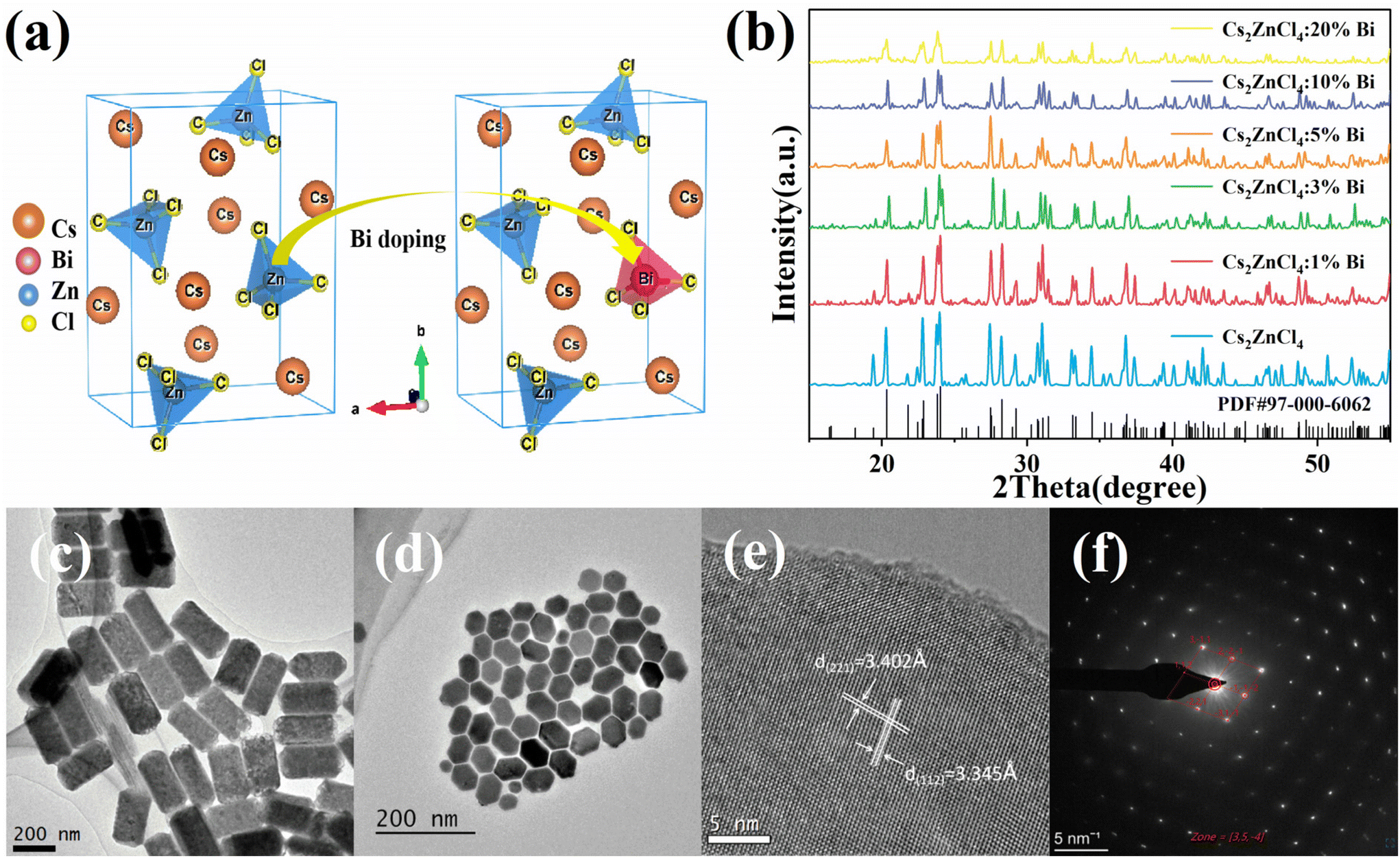 | ||
| Fig. 1 (a) Crystal structures diagram of Cs2ZnCl4 and Bi-doped Cs2ZnCl4 NCs. (b) Comparison of PXRD patterns of Cs2ZnCl4 NCs doped with different contents of Bi3+. TEM images of (c) Cs2ZnCl4 and (d) Cs2ZnCl4:3%Bi NCs. (e) HRTEM images of Cs2ZnCl4:3%Bi NCs. (f) SAED pattern of Cs2ZnCl4:3%Bi NCs. | ||
Photophysical properties of pristine Cs2ZnCl4 and Bi3+-doped Cs2ZnCl4 NCs
To further study the photophysical properties of the materials, UV-Vis absorption spectra and PL spectroscopy of undoped and Bi-doped Cs2ZnCl4 NCs were measured. As shown in Fig. 2a, an exciton absorption peak at 270 nm (4.6 eV) is present in both pristine and Bi3+-doped Cs2ZnCl4 NCs, demonstrating that the main electronic transitions at the band edge were unaffected by the addition of Bi3+. The observed low energy absorption band in the range of 300–400 nm may be related to the defect energy level. A rise in the absorption intensity in the 250–300 nm region appeared when the doping concentration of Bi3+ increased, peaking at 3% Bi3+, which results from the interaction of the host and Bi3+. The corresponding band gaps of Cs2ZnCl4 NCs at different doping concentrations can be calculated by the Tauc plot equation. As shown in Fig. 2b, the band gap of pristine Cs2ZnCl4 NCs is 4.29 eV, which is a wide band gap and direct band gap semiconductor material.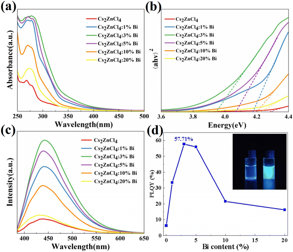 | ||
| Fig. 2 (a) UV-Vis absorption spectra, (b) Tauc plots, (c) PL spectra, and (d) PLQY plots of Cs2ZnCl4 NCs doped with different contents of Bi3+. The inset in (d) shows photographs of Cs2ZnCl4 NCs and Cs2ZnCl4:3% Bi NCs under 365 nm UV. | ||
The band gaps of NCs doped with other concentrations are smaller than the original band gaps, with the Cs2ZnCl4:3%Bi NCs having the smallest band gap of 3.95 eV. The band gap narrows as Bi3+ concentration increases, which correlates to the red shift of the absorption band edge in the absorption spectrum and demonstrates that bismuth is effectively doped into the Cs2ZnCl4 NCs lattice. The band gap of Cs2ZnCl4:Bi NCs is reduced, and the band edges are more localized because the bismuth doping leads to the formation of new defect bands.28 It's also possible that some Bi3+ ions doped into the Cs2ZnCl4 NCs lattice in place of Zn2+ ions have a radius larger than that of Zn2+, expanding the lattice and weakening the Coulomb forces between the ions, resulting in a narrower band gap and a red-shifted absorption spectrum. PL spectra and PLQY show (Fig. 2c and d) that at 365 nm excitation, the original Cs2ZnCl4 NCs exhibit the lowest photoluminescence intensity at room temperature (PLQY = 6.3%), producing very weak broadband emission at 445 nm. The PL intensity of Cs2ZnCl4 NCs was greatly enhanced by modulating the (Bi/Zn) feeding ratio. The PL intensity reaches its maximum (PLQY = 57.71%) at 3% Bi3+, with a wide FWHM of 92 nm and an unchanged PL peak position, showing bright blue emission. When the doping of Bi3+ was continued to be increased, the PL intensity of Cs2ZnCl4:Bi NCs was found to decrease at higher doping concentrations (at Bi concentrations up to 20%, the PLQY value drops to 16.22%). The trend of the PLQY value of Cs2ZnCl4:Bi NCs is compatible with the change of its PL spectral intensity, which both increases initially and subsequently noticeably decreases with the change of the doping element feeding ratio. This phenomenon is attributed to the introduction of excess Bi3+, leading to concentration quenching effect.
The emission wavelength-dependent normalized PL and PLE spectra of Cs2ZnCl4:3%Bi NCs are investigated to gain insight into the origin of the wideband blue emissions. Normally, the excitation energy has a significant impact on the PL spectrum derived from ionoluminescence since excitation and recombination rates greatly rely on ion energy levels and their resonance.36,37 In relation to Bi3+'s ionoluminescence, the external electron configuration of Bi3+ is 5s2, which has five energy levels: the ground state 1S0, the triplet excited state 3P0, 3P1, 3P2 and the singlet excited state 1P1. Based to the electron transition law, under the influence of spin–orbit coupling, the 1S0 → 1P1 transition is allowed, the 1S0 → 3P1 transition is partially allowed, while the 1S0 → 3P2 and 1S0 → 3P0 transitions are completely forbidden at the level of electric dipole transition. Specifically, these forbidden transitions can be disrupted by the lattice vibration.38 Typically, a change in excited energy causes a noticeable peak position shift and shape change for the associated emission.39 The corresponding emission spectra for Cs2ZnCl4:3% Bi NCs revealed tiny peak displacements and shape modifications when the monitoring excited wavelength was changed from 330 to 380 nm (Fig. 3a). Additionally, changing the emission wavelength from 430 to 480 nm (Fig. 3b) resulted in only a negligible shift in the associated excited spectrum. Therefore, it is speculated that Bi3+ ionoluminescence is not the light emission mechanism of broadband blue light emission. The PL intensity of Bi-doped Cs2ZnCl4 NCs exhibit linear relationship with their excitation power, thus excluding the possibility of permanent defects as the origin of photoemission (Fig. S5†).
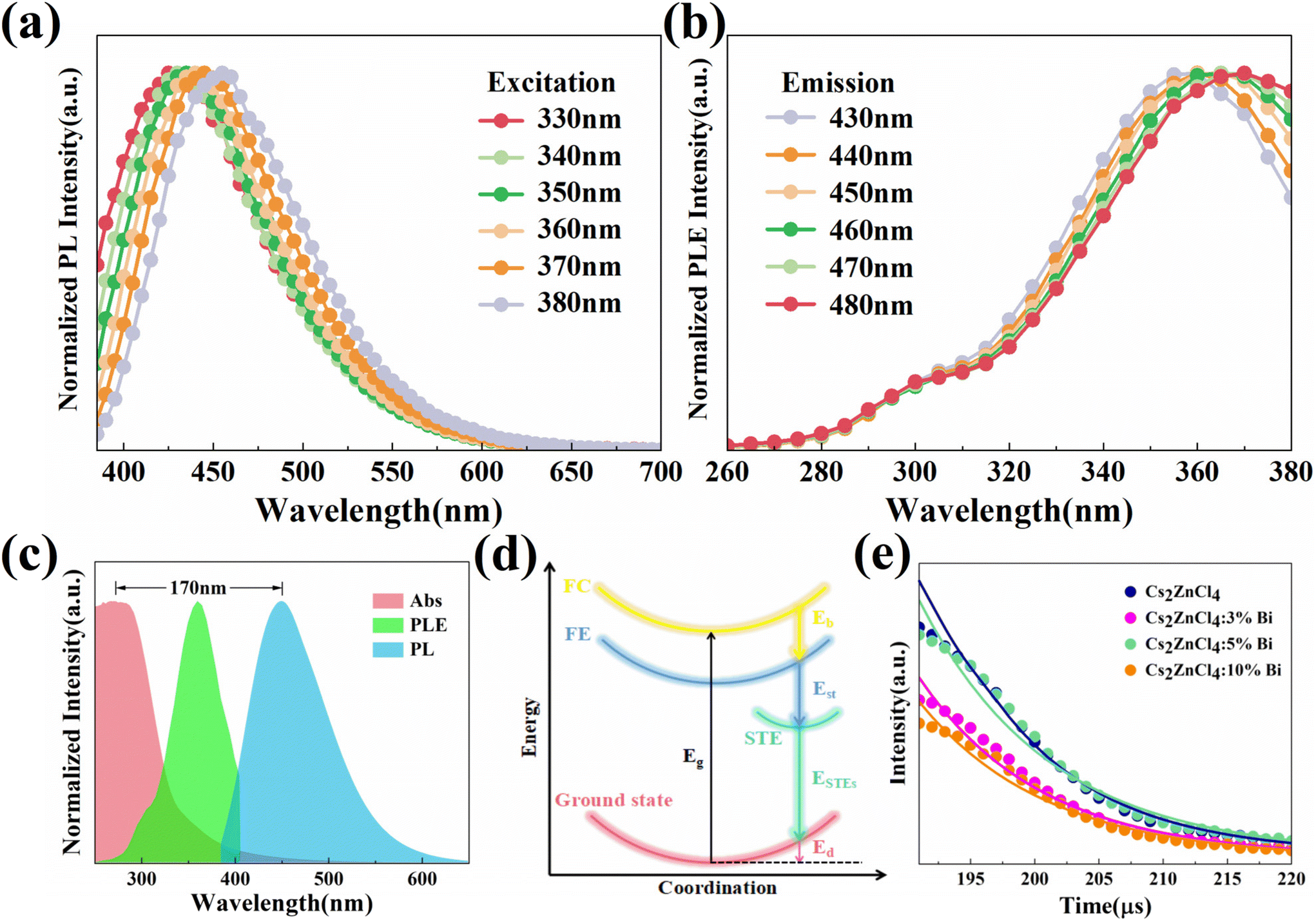 | ||
| Fig. 3 (a) PLE spectra and (b) PL spectra for Cs2ZnCl4:3%Bi NCs. (c) Typical normalized absorption, excitation, and emission spectra of the as-synthesized Cs2ZnCl4:3%Bi NCs. (d) schematic diagram of self-trapping exciton emission. (e) Time-resolved PL spectrum of Cs2ZnCl4 NCs doped with different contents of Bi3+ (excited at 365 nm, monitored at 445 nm). | ||
According to Fig. 3c, the Cs2ZnCl4:3%Bi NCs have a large Stokes shift of 170 nm and a wide FWHM of 92 nm, suggesting that the fluorescence emission may be caused by self-trapped excitons (STEs) emission induced by bismuth ion doping, as is the case for additional zero-dimensional metal halides.40,41 In materials with soft lattices and strong electron–phonon coupling, self-trapping excitons generally arise, and the emission exhibits the typical traits of a broad spectrum with large Stokes shifts. Regarding soft lattice halides, excited photogenerated electrons first couple with the lattice vibrations, causing momentary distortions in the lattice and eventually the production of self-trapped excitons. ESTEs = Eg − Eb − Est − Ed, where Eg is band gap energy and Eb is exciton binding energy, is the formula used to represent the energy of STEs (Fig. 3d). The exciton loses a quantity of energy when producing STEs, which is referred to as self-trapped energy (Est). Lattice deformation causes the energy of the ground state to grow concurrently; this increase is referred to as lattice deformation energy (Ed). There is a significant Stokes shift in the STE emission because the ESTEs is considerably lower than Eg.42 Given that the emission from self-trapped excitons is unaffected by band edge states, it makes sense that bismuth doping would alter the band gap of Cs2ZnCl4 without changing the location of the PL peak.
To further study the luminescence mechanism of NCs, the transient dynamics of their carriers are characterised. The PL decay curve of Cs2ZnCl4 NCs doped with varied amounts of Bi3+ recorded at 445 nm and stimulated by 365 nm light is shown in Fig. 3e. A biexponential function (1) is able to efficiently fit the PL decay line for NCs.
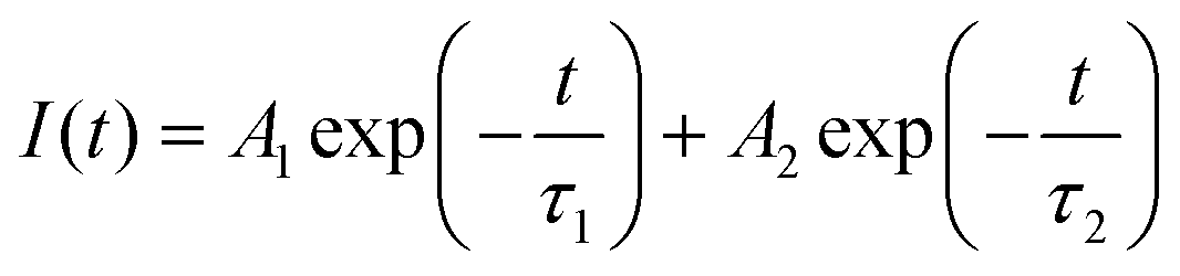 | (1) |
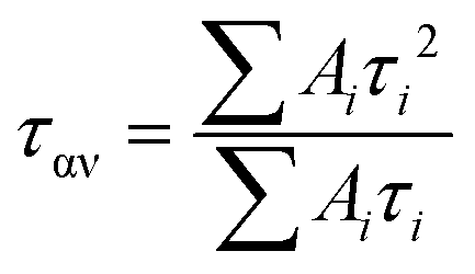 | (2) |
The fitted data are shown in Table 1. The variation of the average lifetime ταν is the result of the competition between different carrier recombination channels at their respective timescales. It can be seen that with the increasing concentration of Bi3+, the proportion A1 of short lifetime τ1 of the doped Cs2ZnCl4 NCs gradually decreases and the proportion A2 of long lifetime τ2 gradually increases. The average lifetime ταν show a slightly monotonical decrease, which is associated with the increase of non-radiative recombination. Undoped Cs2ZnCl4 NCs have a short lifespan τ1 caused by non-radiative recombination brought on by surface flaws, and a long lifespan τ2 related to the recombination of intrinsic self-trapped excitons (intrinsic STEs). The short lifetime τ1 of Bi-doped Cs2ZnCl4 NCs is caused by energy relaxation from the singly excited state 1P1 to the triplet excited state 3P1 through Intersystem Crossing (ISC). The long lifetime τ2 is attributed to the bismuth-doped induced triplet self-trapped excitons (extrinsic STEs) transition from the triplet state 3P1 to the ground state 1S0 in a radiative recombination, which is consistent with previously reported microsecond-scale lifetimes of other low-dimensional metal halides.18 The highest PLQY values of Cs2ZnCl4 NCs were obtained when the Bi3+ doping concentration was 3%, and the highest percentage of short lifetime τ1 caused by the relaxation of the singlet to triplet excited states. The analysis demonstrated that the appropriate amount of Bi3+ doping could generate more STEs while effectively reducing the defect state density of the NCs and improving the fluorescence performance. According to the above research, the photoexcitation causes a quick spread of self-trapped excitons, and by an extremely fast ISC process, the creation of singlet-state STEs is converted into triplet-state self-trapped exciton states, ultimately producing a blue emission that is efficacious, has a long lifespan, and has a significant Stokes shift.
| NCs | τ 1(μs) | A 1 | τ 2 (μs) | A 2 | τ αν (μs) |
|---|---|---|---|---|---|
| Cs2ZnCl4 | 0.70 | 49.76% | 7.34 | 50.24% | 1.29 |
| Cs2ZnCl4:3%Bi | 0.96 | 75.53% | 10.27 | 24.47% | 1.23 |
| Cs2ZnCl4:5%Bi | 0.83 | 65.86% | 7.57 | 34.14% | 1.18 |
| Cs2ZnCl4:10%Bi | 0.78 | 65.35% | 7.52 | 34.65% | 1.13 |
Temperature-dependent photoluminescence
Temperature-dependent PL investigations were made in the range of 10–300 K to shed light on the photophysical characteristics of Cs2ZnCl4:Bi NCs (Fig. 4a–d). Radiative and non-radiative relaxation processes in nanocrystals and exciton-phonon coupling processes can be investigated by fitting analysis of peak intensities, peak energies, and Full width at half maximum (FWHM) to temperature-dependent PL data. The findings demonstrate that as temperature rises, each sample's emission strength gradually declines as a result of excitons’ thermal dissociation inhibiting radiative recombination. When the electron in the excited state obtains energy greater than the thermal activation energy ΔE of the energy level as the temperature rises, it quickly transitions back to the ground state through radiation-free relaxation, which results in thermal quenching.43 In contrast, when the temperature dropped, the PL intensity of all specimens arose. This is attributed to the reduced phonon-exciton coupling and phonon energy transfer chances at low temperatures, resulting in suppressed non-radiative recombination, enhanced radiative recombination and higher luminescence intensities. At the same time, a new broad-shouldered emission peak at 495 nm is also produced, showing a double emission at low temperature. The reason for the double emission at low temperature may be the possible existence of an additional excited state patterns on the potential energy surface of the pristine intrinsic self-trapped exciton, as similar PL spectra is demonstrated in the pristine Cs2ZnCl4 NCs at low temperatures (Fig. 4a). During warming (from 200 K-300 K), the broad-shouldered emission peaking at 495 nm progressively loses strength until it vanishes. The situation shows that the self-trapped exciton can get sufficient thermal energy to cross the energy barrier between both radiating excited states since the temperature is raised, while causing the PL thermal quenching due to exciton thermal dissociation. In addition, the doping of Bi3+ also has an effect on the state of the double emission at low temperatures. Regarding this new emission peak, its emission intensity becomes enhanced when the temperature decreases. In contrast to the pristine Cs2ZnCl4 NCs, where this emission peak is always lower than the original emission peak at 445 nm, the shoulder-like peak in the Cs2ZnCl4:Bi NCs is comparable to the pristine emission peak at 10 K. The reason for the difference in the shoulder emission results at low temperatures may be due to the energy transfer from the triplet excited state induced by the bismuth ion doping in Cs2ZnCl4:Bi NCs to the excited state of the shoulder emission.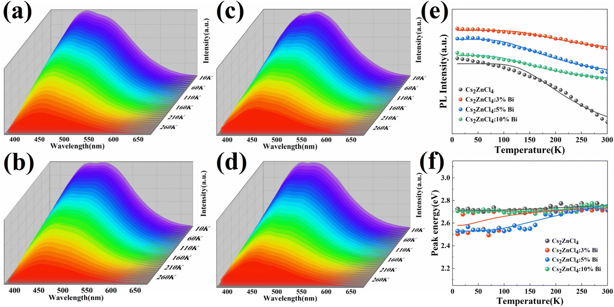 | ||
| Fig. 4 Temperature-dependent PL spectra of (a) Cs2ZnCl4, (b) Cs2ZnCl4:3%Bi, (c) Cs2ZnCl4:5%Bi and (d) Cs2ZnCl4:10%Bi NCs from 10 to 300 K. (e) Fitting results of the integrated intensities of the PL spectra as a function of temperatures. (f) Fitting results of the Peak energies of the PL spectra as a function of temperatures for Cs2ZnCl4:Bi NCs with different Bi3+ concentrations. | ||
As shown in Fig. 4e, we analyzed the PL intensity of Cs2ZnCl4:Bi NCs as a function of temperature to study the non-radiative relaxation mechanism in nanocrystals. The intensity of the emission peaks of the nanocrystals constantly diminishes with the temperature rise due to the thermal quenching process of the excitons.44Table 2 data were fitted applying eqn (3).
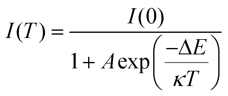 | (3) |
| NCs | ΔE (meV) | A |
|---|---|---|
| Cs22nCl4 | 64.37 | 17.70 |
| Cs22nCl4:3%Bi | 65.00 | 19.89 |
| Cs22nCl4:5%Bi | 41.82 | 5.90 |
| Cs22nCl4:10%Bi | 36.83 | 5.21 |
The exciton binding energy ΔE not only laterally represents the stability of the material but also expresses the rate of change of its PL intensity with temperature, i.e., the larger the ΔE, the less susceptible the PL of its material is to temperature effects. The exciton binding energy ΔE of Cs2ZnCl4:3%Bi NCs in Table 2 is 65 meV, the largest ΔE among the tested samples, and therefore its PL intensity is least affected by temperature variation in the figure, indicating that relatively stable STEs can be formed. The results show that an appropriate amount of Bi3+ doping can increase the exciton binding energy ΔE, because the introduction of Bi3+ generates more self-trapped excitons while effectively reducing the density of defect states in the nanocrystals, which reduces the chance of non-radiative transition and improves the fluorescence performance of the nanocrystals. As shown by the fact that the activation energy determined by fitting the temperature-dependent PL intensity is significantly greater than the thermal energy of perovskites at ambient temperature (26 meV), STEs with a strongly localized action are stable.45
In order to understand the effect of exciton-phonon coupling on the optical properties of nanocrystals, we examined the relationship between the PL peak energy of Cs2ZnCl4:Bi NCs and temperature, as depicted in Fig. 4f. Table 3 contains a list of the outcomes from fitting eqn (4).
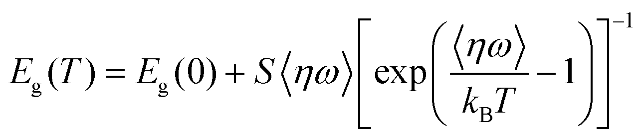 | (4) |
| NCs | E g(0) (eV) | S | 〈ηω〉 (meV) |
|---|---|---|---|
| Cs2ZnCl4 | 2.71 | 1.72 | 34.86 |
| Cs2ZnCl4:3%Bi | 2.58 | 9.28 | 8.38 |
| Cs2ZnCl4:5%Bi | 2.53 | 8.97 | 27.95 |
| Cs2ZnCl4:10%Bi | 2.70 | 5.08 | 73.84 |
For Cs2ZnCl4:Bi NCs, its PL emission peak position is blue-shifted with increasing temperature. Interpreting the temperature dependence of PL peak shift in solid semiconductors in terms of lattice expansion and electron–phonon coupling.48 In common, the band gap can narrow as temperature rises due to electron–phonon interaction. For lead halide perovskites, lattice expansion induce band gap blue shifting due to the presence of bonding and anti-bonding orbitals in the band.49 The peak positions of 3% and 5% Bi3+ doped Cs2ZnCl4 NCs in the figure vary more as the temperature rises, which results from the strong electron–phonon coupling in the matrix, but also due to the significant shift of the highest peak position caused by the double emission generated at low temperature. In addition, the FWHM was observed to become smaller with higher temperature by fitting the temperature-dependent FWHM fluctuation (Fig. S6†). The disappearance of the double emission of Cs2ZnCl4 NCs at room temperature and the change of the PL spectral line from the overlapping double peak at low temperature to a single peak are responsible for the narrowing of the FWHM.
DFT calculation for optoelectronic and photophysical properties
In order to investigate in depth the electronic states and photophysical characteristics of Bi integrated in Cs2ZnCl4 NCs and their effects, first-principles DFT calculations were performed. The substituted model calculated here is built on the basis of the pristine model by substituting one Bi3+ for one Zn2+ while generating one Cs vacancy (V’Cs). Fig. 5 shows the calculated static charge-density, electron energy band structure and density of states (DOS), and pristine Cs2ZnCl4 NCs energy band shape and band type consistent with the literature.18 From Fig. 5c, the bandgap of the original Cs2ZnCl4 NCs is 4.6 eV, which is a direct bandgap. According to the DOS analysis of Cs2ZnCl4 NCs (Fig. 5e), Cl-p, Zn-d orbitals and Zn-s, Cl-p orbitals, respectively, made up the majority of the top and bottom of the valence band and conduction band. Substantial wavefunction deviations in the Zn-s and Cl-p orbitals, as well as substantial dispersion, are present in the conduction band. The DOS analysis of the Cs2ZnCl4:Bi NCs shows that the VBM consists mainly of a combination of Cl-p and Zn-d orbitals. The doping of Bi3+ forms a defect band consisting mainly of Bi-p and Cl-p orbitals at 2.5 eV above the VBM (Fig. 5d and f). It is worth noting that the band gap in this region (2.5 eV) is in good agreement with the observed PL emission (2.76 eV, Fig. 2c), considering that the DFT-PBE function calculation underestimates the band gap. The lowest state of the conduction band consisting of Bi-p and Cl-p orbitals was strongly localized in the tetrahedral [BiCl4]−, and these results suggest that the spin-triplet exciton may be trapped at [BiCl4]− unit (consistent with the experimentally observed microsecond-scale decay times) and provide a channel for effective emission.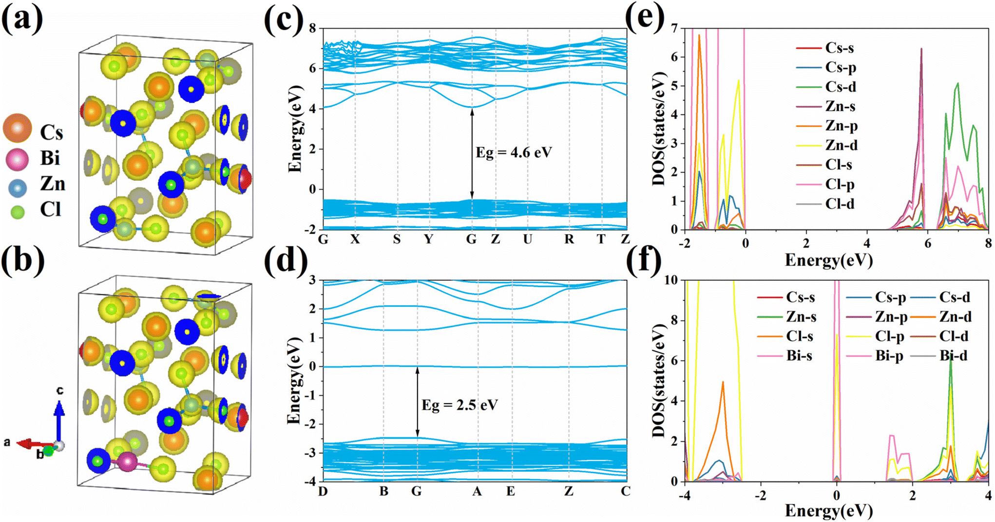 | ||
| Fig. 5 (a and b) Calculated static charge-density, (c and d) calculated electronic band structure and (e and f) calculated PDOS of pristine Cs2ZnCl4 and Cs2ZnCl4:Bi3+ NCs, respectively. | ||
PL recombination mechanism of pristine Cs2ZnCl4 and Bi3+-doped Cs2ZnCl4 NCs
In summary, the photoluminescence mechanism of Cs2ZnCl4:Bi NCs can be explained in Fig. 6 by analysing the optical properties and DFT calculations. At room temperature (Fig. 6a), under the excitation of photon energy at 300 nm and 365 nm, the ground state electrons are excited to the ES1, and electrons go through a speedy transmission of energy (ET1) and subsequently return to the ground state through intrinsic STEs-1 radiation transition. The weaker exciton-phonon coupling of the Cs2ZnCl4 host leads to a smaller chance of distortion of [ZnCl4]2− tetrahedras, which produces fewer intrinsic STEs, as well as more defects that inhibit radiative recombination and lead to low PLQY. In Bi3+-doped host, the ground state electrons are excited to the ES1, the singlet-state (ES3), and the triple excited state of Bi3+ (ES4). The electrons go through a speedy transmission of energy (ET1), (ET2), and (ET3), then extrinsic STEs are generated in ES4 by [BiCl4]− tetrahedral distortion. Finally, the radiative transition from extrinsic STEs to the 1S0 ground state of Bi3+ results in high-efficiency extrinsic STEs radiation that exhibits a notable Stokes shift. The other small fraction of electrons back to the ground state by intrinsic STEs-1 radiation transition. At low temperatures (Fig. 6b), in addition to the above recombination process, a new lower potential energy intrinsic STEs-2 is generated next to the intrinsic STEs-1 in the Cs2ZnCl4 matrix, which is manifested in the PL pattern as a double emission at low temperature. At low temperature, the intensity of the shoulder peak of Bi-doped samples starts to increase relative to the main emission peak, which may be attributed to the introduction of bismuth ions effectively eliminating the nonradiative recombination and the energy transfer from the triple-excited state 3P1 of Bi3+ ions to the intrinsic STEs-2.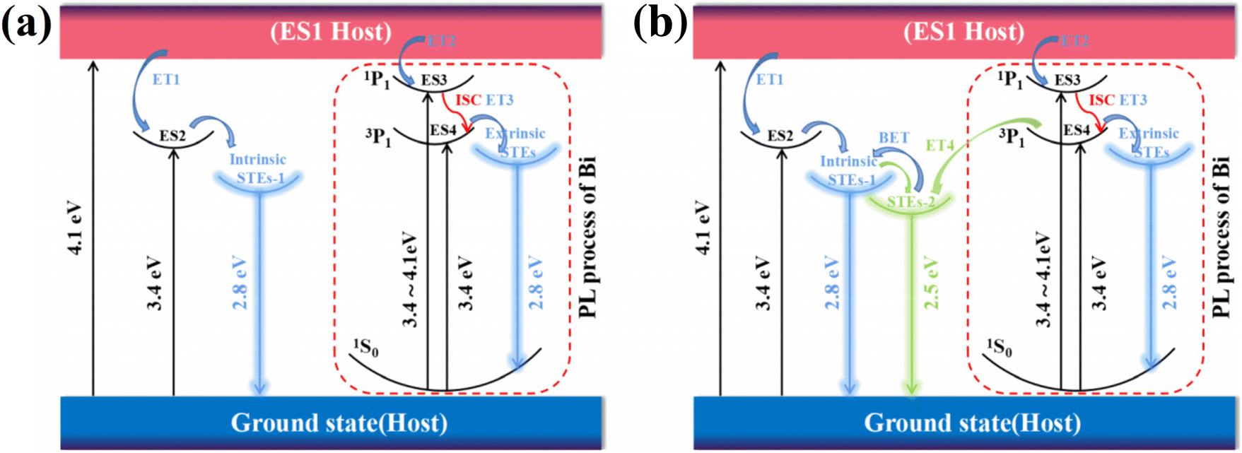 | ||
| Fig. 6 Schematic illustration of PL recombination mechanism in Cs2ZnCl4:Bi3+at (a) room temperature and (b) low temperature, respectively. ES1: excited state of Cs2ZnCl4 at high energy level (at 300 nm excitation); ES2: excited state of Cs2ZnCl4 at low energy level (at 365 nm excitation); ES3: singly excited states of Bi3+ (corresponding to 300–365 nm); ES4: triplet excited states of Bi3+ (at 365 nm excitation); ET1: transmission of energy from ES1 to ES2; ET2: transmission of energy from ES1 to ES3; ET3: energy relaxation from the singly excited state 1P1 to the triplet excited state 3P1 in the form of Intersystem Crossing (ISC); ET4: transmission of energy from ES4 to intrinsic STEs-2; BET: back energy transfer from intrinsic STEs-2 to intrinsic STEs-1. The green arrows indicate processes that occur only at low temperatures. | ||
During warming, the broad-shouldered emission peak at 495 nm begins to fade away, suggesting a possible back energy transfer (BET) from intrinsic STEs-2 to intrinsic STEs-1.
We suggest that the pristine material exhibits weak luminescence due to non-radiative relaxation induced by inherent defects and a limited number of intrinsic self-trapped exciton complex channels. As a consequence, the material experiences a low transition probability of radiation, leading to an extremely low PLQY. For Cs2ZnCl4:Bi3+ NCs, because of the strong exciton-phonon coupling impact of Bi3+ doping in the matrix, the probability of distortion of the [BiCl4]− tetrahedron increases as the luminescence center becomes larger, which makes it easy to form STEs. Strong quantum confinement strongly traps photogenerated carriers in these separated tetrahedra, whereas defects are passivated in favor of radiative recombination, resulting in enhanced PLQY.
Antiwater stability of Cs2ZnCl4:Bi NCs
Further research on the antiwater stability of Cs2ZnCl4:Bi NCs is necessary since the stability of the nanocrystals is closely related to the application. The PL spectra (Fig. 7a and b) of pristine and Bi-doped Cs2ZnCl4 NCs aqueous solutions were measured at various intervals after thorough stirring under ambient atmosphere, following the addition of 1 ml of deionized water to the solutions. The PL intensity of Cs2ZnCl4 NCs degraded to 49% of the original after 100 minutes immersed in deionized water; however Cs2ZnCl4:Bi NCs maintained 82% of the original PL intensity (Fig. 7c). We then performed FTIR spectra to characterize the chemical bonds of the soaked samples. In contrast to the undoped sample, a characteristic peak appears at 513 cm−1 in the Bi-doped sample, which corresponds to Bi–O bonds (Fig. 7d). Therefore, we suggest that water induces surface hydrolysis of Cs2ZnCl4:Bi NCs to form a BiOCl protective layer that encapsulates the luminescent material against further water corrosion, resulting in excellent water stability, similar to the previously reported water-induced BiOBr passivation of Bi-based perovskites Cs3Bi2Br9.34 In addition, the samples were tested for thermal and optical stability, and the results showed that the doped samples performed better than the pristine samples (Fig. S7†).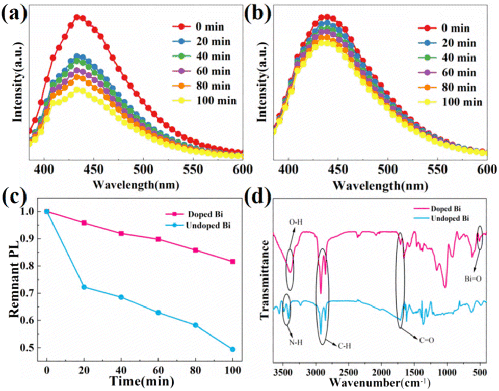 | ||
| Fig. 7 (a and b) Antiwater stability and (c) Remnant PL spectra of pristine and Bi-doped Cs2ZnCl4 NCs immersed in deionized water for different durations. (d) FTIR spectra of Bi-doped and pristine Cs2ZnCl4 NCs before and after immersion. | ||
Fabrication and evaluation of photovoltaic modules with down-converting layers and blue light LED devices
With respect to their simplicity of construction and benefits in terms of cost-competitiveness, photovoltaic (PV) cells and modules, which produce power from the plentiful sunlight at the planet's surface, have been regarded as one of the most alluring green power innovations. To further improve the photovoltaic (PV) cell's photovoltaic conversion efficiency, a luminescent down-shift layer (LDS) can be implanted on surface of the cell to solve the problem of poor absorption of solar cells at short wavelengths by using the down-conversion principle.50 Therefore, considering that the EQE of GaAs solar cells is greater than 80% in the visible region of 400–900 nm,51 Cs2ZnCl4:Bi NCs can be used to transform high energy ultraviolet (UV) rays into low energy visible light, which can be made into a luminescent down-shift layer and combined with an aviation GaAs solar cell (Product no: HGSC-A100B-1S, hasunopto Co, Ltd), as shown in Fig. 8a. In this device structure, the incident sunlight follows the following three paths.52 (i) Incident light is reflected at the interlayer interface on the front surface due to differences in refractive index. (ii) Incident light is absorbed and re-emitted by perovskite emitters. (iii) Incident light penetrates the front layer and is absorbed and converted to electricity by the active layer in the solar cell. In order to reduce the solar cell's surface reflection, the perovskite nanoparticles are evenly scattered on top of the surface.53 According to Table 4, the GaAs solar cell's initial PCE value was 30.2%. After the Cs2ZnCl4:Bi NCs-LDS layers were applied to the solar cell surface, the PCE value was increased by 1% to 31.2%. The increase in PCE efficiency is due to the enhanced absorption of Cs2ZnCl4:Bi NCs in the UV region, which can convert incident high-energy sunlight into a broad spectrum of visible light more suitable for absorption by PV modules, further increasing the conversion efficiency of the PV device (Fig. S8†). Fig. 8c–e show photos of the solar cell featuring perovskite LDS layers taken using thermal imaging. In the presence of daylight, the surface temperature of the PV cell rises rapidly. After 10 minutes of light exposure, the surface temperature of the PV cell with and without the addition of the perovskites down-conversion coating was 42.6 °C and 41 °C, respectively. The perovskites absorbed a tiny quantity of thermal energy, though it didn't affect the PV cell's PCE. Additionally, in situations with high temperatures, PV modules covered with perovskites maintained a high PCE.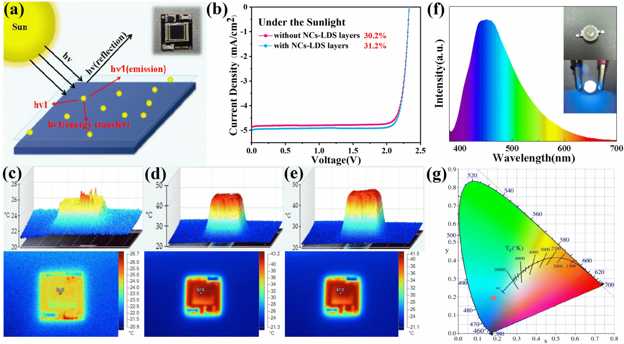 | ||
| Fig. 8 (a) Diagrammatic representation of the construction of solar cell using LDS layer and mode of operation in daylight. (b) J–V characteristics of solar cells with and without Cs2ZnCl4:Bi NCs in daylight. (c) Photos of the solar cell featuring perovskite LDS layers taken using thermal imaging in a dark setting. (d) Photos of the solar cell using perovskite LDS layers taken using thermal imaging after ten minutes of exposure to the sun. (e) Photos of the solar cell without perovskite LDS layers taken using thermal imaging after ten minutes of exposure to the sun. (f) Emission spectrum of the LED based on Cs2ZnCl4:3%Bi. Inserts show the photographs of LED device of power on/off. (g) CIE chromaticity diagram corresponding to emission spectrum. | ||
| Under the sunlight | I SC (mA) | V OC (V) | FF | P max (mW) | PCE (%) |
|---|---|---|---|---|---|
| Without NCs-LDS layers | 4.9 | 2.3 | 0.86 | 9.7 | 30.2 |
| With NCs-LDS layers | 5.0 | 2.3 | 0.87 | 10 | 31.2 |
In this study, the produced Cs2ZnCl4:Bi NCs were evenly blended with epoxy glue and covered on a commercial 365 nm GaN LED chip before being dried and cured to make blue-light LED devices. The power on/off effects and electroluminescence (EL) spectra of the LED devices are shown in Fig. 8f. The color coordinates (CIE1931) were calculated to be (0.1815, 0.1927), as shown in Fig. 8g. Finally, the LEDs based on Cs2ZnCl4:Bi NCs emit a bright broad-spectrum blue light centered at 450 nm when energized. The stability of the LED device is shown in Fig S9.† In biomedicine, antibacterial blue light in the 400–470 nm spectrum has proven its intrinsic antimicrobial properties to inactivate bacteria and viruses.54 These results demonstrate the potential application of broad-spectrum blue light emission from 0D all-inorganic metal halide Cs2ZnCl4:Bi3+ NCs in photovoltaic power generation, solid-state lighting, and biomedicine.
Conclusions
In summary, we have synthesized Bi-doped all-inorganic lead-free perovskites Cs2ZnCl4 NCs by a green and facile process using thermal injection. The pristine Cs2ZnCl4 NCs were originally weakly luminescent (PLQY = 6.3%), but by adjusting the stoichiometric ratio of the doped elements to find the optimum feeding ratio for luminescence efficiency (Bi/Zn = 3/100), the doped samples exhibited highly efficient blue broad emission at 445 nm (PLQY = 57.71%). Detailed spectral characterization including time-resolved PL, temperature-dependent PL, and first-principles DFT calculations, indicate that the triplet-state STEs emission caused by bismuth ion doping is the source of the bright broad-spectrum blue light emission. The Cs2ZnCl4:Bi NCs exhibited good water stability as a result of the self-passivation of water-induced generation of BiOCl. Photovoltaic cell modules fabricated with Cs2ZnCl4:Bi3+ NCs for down-conversion coating exhibited excellent performance. Regarding the future development of new energy photovoltaic devices, it offers a sustainable and effective approach. In addition, Bi-doped Cs2ZnCl4 NCs combined with commercial 365 nm GaN LED chips can be assembled into broad-spectrum blue-emitting LED devices. As a result, we think Cs2ZnCl4:Bi NCs offer enormous promise for the development of innovative lead-free perovskites optoelectronic devices.Conflicts of interest
There are no conflicts to declare.Acknowledgements
This work was financial supported in part by the Tianjin Natural Science Foundation (No. 17JCQNJC02300 and 18JCYBJC86200), National Natural Science Foundation of China (No. 51702235, 51871167, and 51971158), the National Key Foundation for Exploring Scientific Instrument of China (No. 2014YQ120351), and Scientific Developing Foundation of Tianjin Education Commission (No. 2017ZD14 and 2018ZD09).References
- Y. Gao, C. Yan, X. Peng, W. Li, J. Cao, Q. Wang, X. Zeng, X. Fu and W. Yang, The metal doping strategy in all inorganic lead halide perovskites: synthesis, physicochemical properties, and optoelectronic applications, Nanoscale, 2021, 13, 18010–18031 RSC.
- Y. Shi, W. Zhao, Z. Ma, G. Xiao and B. Zou, Self-trapped exciton emission and piezochromism in conventional 3D lead bromide perovskite nanocrystals under high pressure, Chem. Sci., 2021, 12, 14711–14717 RSC.
- M. Li, S. Peng, S. Fang, Y. Gong, D. Yang, K. Bu, B. Liu, H. Luo, S. Guo, J. Li, H. Wang, Y. Liu, S. Jiang, C. Lin and X. Lü, Synthesis of Two-Dimensional CsPb2X5 (X = Br and I) with a Stable Structure and Tunable Bandgap by CsPbX3 Phase Separation, J. Phys. Chem. Lett., 2022, 13, 2555–2562 CrossRef CAS PubMed.
- W. Liu, M. Cao, J. Zhang, J. Jiang, H. Yu, X. Hao, J. Zhang, H. Guo, B. Fang, N. Yuan, X. Fan, S. Zhang and J. Ding, Reversible degradation-assisted interface engineering via Cs4PbBr6 nanocrystals to boost the performance of CsPbI2Br perovskite solar cells, J. Power Sources, 2022, 530, 231294 CrossRef CAS.
- M. Mateen, Z. Arain, Y. Yang, X. Liu, S. Ma, C. Liu, Y. Ding, X. Ding, M. Cai and S. Dai, MACl-Induced Intermediate Engineering for High-Performance Mixed-Cation Perovskite Solar Cells, ACS Appl. Mater. Interfaces, 2020, 12, 10535–10543 CrossRef CAS PubMed.
- H. Shimizu, in LED Lighting for Urban Agriculture, ed. T. Kozai, K. Fujiwara and E. S. Runkle, Springer Singapore, Singapore, 2016, pp. 239–260, DOI:10.1007/978-981-10-1848-0_18.
- J. Shen, N. Meng, J. Chen, Y. Zhu, X. Yang, Y. Jia and C. Li, Polyacrylic acid-b-polystyrene-passivated CsPbBr3 perovskite quantum dots with high photoluminescence quantum yield for light-emitting diodes, Chem. Commun., 2022, 58, 4235–4238 RSC.
- M. Gong, D. Jiang, T. Tao, F. Chen, C. Xu, T. Zhi, W. Liu, B. Liu, R. Zhang and Y. Zheng, Surface plasmon coupling regulated CsPbBr3 perovskite lasers in a metal-insulator-semiconductor structure, RSC Adv., 2021, 11, 37218–37224 RSC.
- C. H. Kang, O. Alkhazragi, L. Sinatra, S. Alshaibani, Y. Wang, K. H. Li, M. Kong, M. Lutfullin, O. M. Bakr, T. K. Ng and B. S. Ooi, All-inorganic halide-perovskite polymer-fiber-photodetector for high-speed optical wireless communication, Opt. Express, 2022, 30, 9823–9840 CrossRef CAS PubMed.
- Q. A. Akkerman, G. Rainò, M. V. Kovalenko and L. Manna, Genesis, challenges and opportunities for colloidal lead halide perovskite nanocrystals, Nat. Mater., 2018, 17, 394–405 CrossRef CAS PubMed.
- T. C. Jellicoe, J. M. Richter, H. F. J. Glass, M. Tabachnyk, R. Brady, S. E. Dutton, A. Rao, R. H. Friend, D. Credgington, N. C. Greenham and M. L. Böhm, Synthesis and Optical Properties of Lead-Free Cesium Tin Halide Perovskite Nanocrystals, J. Am. Chem. Soc., 2016, 138, 2941–2944 CrossRef CAS PubMed.
- A. Wang, X. Yan, M. Zhang, S. Sun, M. Yang, W. Shen, X. Pan, P. Wang and Z. Deng, Controlled Synthesis of Lead-Free and Stable Perovskite Derivative Cs2SnI6 Nanocrystals via a Facile Hot-Injection Process, Chem. Mater., 2016, 28, 8132–8140 CrossRef CAS.
- J. Zhang, Y. Yang, H. Deng, U. Farooq, X. Yang, J. Khan, J. Tang and H. Song, High Quantum Yield Blue Emission from Lead-Free Inorganic Antimony Halide Perovskite Colloidal Quantum Dots, ACS Nano, 2017, 11, 9294–9302 CrossRef CAS PubMed.
- M. Leng, Z. Chen, Y. Yang, Z. Li, K. Zeng, K. Li, G. Niu, Y. He, Q. Zhou and J. Tang, Lead-Free, Blue Emitting Bismuth Halide Perovskite Quantum Dots, Angew. Chem., Int. Ed., 2016, 55, 15012–15016 CrossRef CAS PubMed.
- B. M. Benin, D. N. Dirin, V. Morad, M. Wörle, S. Yakunin, G. Rainò, O. Nazarenko, M. Fischer, I. Infante and M. V. Kovalenko, Highly Emissive Self-Trapped Excitons in Fully Inorganic Zero-Dimensional Tin Halides, Angew. Chem., Int. Ed., 2018, 57, 11329–11333 CrossRef CAS PubMed.
- T. Jun, K. Sim, S. Iimura, M. Sasase, H. Kamioka, J. Kim and H. Hosono, Lead-Free Highly Efficient Blue-Emitting Cs3Cu2I5 with 0D Electronic Structure, Adv. Mater., 2018, 30, 1804547 CrossRef PubMed.
- P. Cheng, L. Feng, Y. Liu, D. Zheng, Y. Sang, W. Zhao, Y. Yang, S. Yang, D. Wei, G. Wang and K. Han, Doped Zero-Dimensional Cesium Zinc Halides for High-Efficiency Blue Light Emission, Angew. Chem., Int. Ed., 2020, 59, 21414–21418 CrossRef CAS PubMed.
- B. Su, M. Li, E. Song and Z. Xia, Sb3+–Doping in Cesium Zinc Halides Single Crystals Enabling High–Efficiency Near–Infrared Emission, Adv. Funct. Mater., 2021, 31, 2105316 CrossRef CAS.
- D. Zhu, M. L. Zaffalon, V. Pinchetti, R. Brescia, F. Moro, M. Fasoli, M. Fanciulli, A. Tang, I. Infante, L. De Trizio, S. Brovelli and L. Manna, Bright Blue Emitting Cu-Doped Cs2ZnCl4 Colloidal Nanocrystals, Chem. Mater., 2020, 32, 5897–5903 CrossRef CAS PubMed.
- V. Morad, I. Cherniukh, L. Pöttschacher, Y. Shynkarenko, S. Yakunin and M. V. Kovalenko, Manganese(II) in Tetrahedral Halide Environment: Factors Governing Bright Green Luminescence, Chem. Mater., 2019, 31, 10161–10169 CrossRef CAS PubMed.
- R. Begum, M. R. Parida, A. L. Abdelhady, B. Murali, N. M. Alyami, G. H. Ahmed, M. N. Hedhili, O. M. Bakr and O. F. Mohammed, Engineering Interfacial Charge Transfer in CsPbBr3 Perovskite Nanocrystals by Heterovalent Doping, J. Am. Chem. Soc., 2017, 139, 731–737 CrossRef CAS PubMed.
- W.-J. Yin, T. Shi and Y. Yan, Unusual defect physics in CH3NH3PbI3 perovskite solar cell absorber, Appl. Phys. Lett., 2014, 104, 063903 CrossRef.
- L. Wang, W. Zheng, F. Vitale, X. Zhang, X. Li, Y. Ji, Z. Liu, O. Ghaebi, C. T. Plass, R. Domes, T. Frosch, G. Soavi, E. Wendler, Y. Zhang and C. Ronning, Wide-Bandgap Double Perovskites with Multiple Longitudinal-Optical Phonon Scattering, Adv. Funct. Mater., 2022, 32, 2111338 CrossRef CAS.
- Q. Huang, Z. Liang, F. Qi, N. Zhang, J. Yang, J. Liu, C. Tian, C. Fu, X. Tang, D. Wu, J. Wang, X. Wang and W. Chen, Carbon Dioxide Conversion Synergistically Activated by Dielectric Barrier Discharge Plasma and the CsPbBr3@TiO2 Photocatalyst, J. Phys. Chem. Lett., 2022, 13, 2418–2427 CrossRef CAS PubMed.
- C. Yang, C. Fan, F. Hussain, Z. Ye, W. Sheng, K. Song, R. Muhammad, J. Wu, Q. Huang, H. Wang, W. Su, J. Xu, S. Sun and D. Wang, Sn4+ induced Bi3+ multi-lattice selective occupation and its color-tunable emission of La2MgZrO6: Bi3+, Sn4+ double perovskite phosphors, J. Alloys Compd., 2022, 902, 163724 CrossRef CAS.
- Y. Zhang, N. Sui, Z. Kang, X. Meng, L. Yuan, X. Li, H.-Z. Zhang, J. Zhang and Y. Wang, Scanning the optoelectronic properties of Cs4CuxAg2–2xSb2Cl12 double perovskite nanocrystals: the role of Cu2+ content, J. Mater. Chem. C, 2022, 10, 5526–5533 RSC.
- Z. Li, Z. Rao, Q. Li, L. Zhou, X. Zhao and X. Gong, Cs2Zr1−xTexCl6 Perovskite Microcrystals with Ultrahigh Photoluminescence Quantum Efficiency of 79.46% for High Light Efficiency White Light Emitting Diodes, Adv. Opt. Mater., 2021, 9, 2100804 CrossRef CAS.
- Z. Tan, J. Li, C. Zhang, Z. Li, Q. Hu, Z. Xiao, T. Kamiya, H. Hosono, G. Niu, E. Lifshitz, Y. Cheng and J. Tang, Highly Efficient Blue-Emitting Bi-Doped Cs2SnCl6 Perovskite Variant: Photoluminescence Induced by Impurity Doping, Adv. Funct. Mater., 2018, 28, 1801131 CrossRef.
- J. A. McGinnety, Crystal structure, crystal forces, and charge distribution in salts of the tetrachlorozincate anion, Inorg. Chem., 1974, 13, 1057–1061 CrossRef CAS.
- N. Ding, L. Shao, T. Xie, G. Pan, D. Zhou, X. Bai, S. Lu, J. Hu, J. Zhou, W. Xu and H. Song, Highly-Sensitive, Stable, and Fast-Response Lead-Free Cs2AgBiBr6 Double Perovskite Photodetectors Enabled by Synergistic Engineering of Doping Na+/Ce3+ and Integrating Ag Nanoparticles Film, Laser & Photonics Reviews, 2022, 16, 2200301 Search PubMed.
- N. Ding, Y. Wu, W. Xu, J. Lyu, Y. Wang, L. Zi, L. Shao, R. Sun, N. Wang, S. Liu, D. Zhou, X. Bai, J. Zhou and H. Song, A novel approach for designing efficient broadband photodetectors expanding from deep ultraviolet to near infrared, Light: Sci. Appl., 2022, 11, 91 CrossRef CAS PubMed.
- N. Ding, W. Xu, D. Zhou, Y. Ji, Y. Wang, R. Sun, X. Bai, J. Zhou and H. Song, Extremely efficient quantum-cutting Cr3+, Ce3+, Yb3+ tridoped perovskite quantum dots for highly enhancing the ultraviolet response of Silicon photodetectors with external quantum efficiency exceeding 70%, Nano Energy, 2020, 78, 105278 CrossRef CAS.
- W. Xu, J. Liu, B. Dong, J. Huang, H. Shi, X. Xue and M. Liu, Atomic-scale imaging of ytterbium ions in lead halide perovskites, Sci. Adv., 2023, 9, eadi7931 CrossRef CAS PubMed.
- M. Leng, Y. Yang, K. Zeng, Z. Chen, Z. Tan, S. Li, J. Li, B. Xu, D. Li, M. P. Hautzinger, Y. Fu, T. Zhai, L. Xu, G. Niu, S. Jin and J. Tang, All-Inorganic Bismuth-Based Perovskite Quantum Dots with Bright Blue Photoluminescence and Excellent Stability, Adv. Funct. Mater., 2018, 28, 1704446 CrossRef.
- N. Hurley, F. Moretti, H. Yan, E. Bourret-Courchesne, Y. S. Chu and S. S. Wong, Devising novel methods for the controlled synthesis with morphology and size control of scintillator materials, J. Mater. Chem. C, 2020, 8, 8622–8634 RSC.
- S. Zhou, N. Jiang, B. Zhu, H. Yang, S. Ye, G. Lakshminarayana, J. Hao and J. Qiu, Multifunctional Bismuth-Doped Nanoporous Silica Glass: From Blue-Green, Orange, Red, and White Light Sources to Ultra-Broadband Infrared Amplifiers, Adv. Funct. Mater., 2008, 18, 1407–1413 CrossRef CAS.
- K. Li, J. Fan, M. Shang, H. Lian and J. Lin, Sr2Y8(SiO4)6O2:Bi3+/Eu3+: a single-component white-emitting phosphor via energy transfer for UV w-LEDs, J. Mater. Chem. C, 2015, 3, 9989–9998 RSC.
- A. Wolfert and G. Blasse, Luminescence of Bi3+-doped crystals of Cs2NaYBr6 and Cs2NaLaCl6, J. Solid State Chem., 1985, 59, 133–142 CrossRef CAS.
- F. Kang, Y. Zhang and M. Peng, Controlling the Energy Transfer via Multi Luminescent Centers to Achieve White Light/Tunable Emissions in a Single-Phased X2−Type Y2SiO5:Eu3+,Bi3+ Phosphor For Ultraviolet Converted LEDs, Inorg. Chem., 2015, 54, 1462–1473 CrossRef CAS PubMed.
- E. R. Dohner, A. Jaffe, L. R. Bradshaw and H. I. Karunadasa, Intrinsic White-Light Emission from Layered Hybrid Perovskites, J. Am. Chem. Soc., 2014, 136, 13154–13157 CrossRef CAS PubMed.
- E. R. Dohner, E. T. Hoke and H. I. Karunadasa, Self-Assembly of Broadband White-Light Emitters, J. Am. Chem. Soc., 2014, 136, 1718–1721 CrossRef CAS PubMed.
- S. Li, J. Luo, J. Liu and J. Tang, Self-Trapped Excitons in All-Inorganic Halide Perovskites: Fundamentals, Status, and Potential Applications, J. Phys. Chem. Lett., 2019, 10, 1999–2007 CrossRef CAS PubMed.
- Q. Ding, X. Zhang, L. Li, X. Lou, J. Xu, P. Zhou and M. Yan, Temperature dependent photoluminescence of composition tunable ZnXAgInSe quantum dots and temperature sensor application, Opt. Express, 2017, 25, 19065–19076 CrossRef PubMed.
- C. Ji, Y. Zhang, T. Zhang, W. Liu, X. Zhang, H. Shen, Y. Wang, W. Gao, Y. Wang, J. Zhao and W. W. Yu, Temperature-Dependent Photoluminescence of Ag2Se Quantum Dots, J. Phys. Chem. C, 2015, 119, 13841–13846 CrossRef CAS.
- R. Zeng, K. Bai, Q. Wei, T. Chang, J. Yan, B. Ke, J. Huang, L. Wang, W. Zhou, S. Cao, J. Zhao and B. Zou, Boosting triplet self-trapped exciton emission in Te(IV)-doped Cs2SnCl6 perovskite variants, Nano Res., 2021, 14, 1551–1558 CrossRef CAS.
- K. Song and R. T. Williams, Self-trapped excitons, 2013 Search PubMed.
- J. Luo, X. Wang, S. Li, J. Liu, Y. Guo, G. Niu, L. Yao, Y. Fu, L. Gao, Q. Dong, C. Zhao, M. Leng, F. Ma, W. Liang, L. Wang, S. Jin, J. Han, L. Zhang, J. Etheridge, J. Wang, Y. Yan, E. H. Sargent and J. Tang, Efficient and stable emission of warm-white light from lead-free halide double perovskites, Nature, 2018, 563, 541–545 CrossRef CAS PubMed.
- X. K. Gong, X. S. Zhang, X. Liu, R. K. Ding, J. J. Zhang, H. Yin, Z. W. Zhang, L. Li and J. P. Xu, Novel cryogenic dual-emission mechanism of lead-free double perovskite Cs2AgInCl6 and using SiO2 to enhance their photoluminescence and photostability, J. Hazard. Mater., 2021, 403, 123821 CrossRef CAS PubMed.
- A. Shinde, R. Gahlaut and S. Mahamuni, Low-Temperature Photoluminescence Studies of CsPbBr3 Quantum Dots, J. Phys. Chem. C, 2017, 121, 14872–14878 CrossRef CAS.
- B. G. Jeong, D. Hahm, J. W. Park, J. Y. Kim, H.-E. Song, M. G. Kang, S. Jeong, G. Kang, W. K. Bae and H.-J. Song, Colorful opaque photovoltaic modules with down-converting InP/ZnSexS1-x quantum dot layers, Nano Energy, 2020, 77, 105169 CrossRef CAS.
- S. Yang, S. Huang, Q. Wang, R. Wu, Q. Han and W. Wu, Temperature-dependent photoluminescence of Cs2AgxNa1−-xInCl6 microcrystals, Opt. Mater., 2019, 98, 109444 CrossRef CAS.
- G. Shao, C. Lou and D. Xiao, Enhancing the efficiency of solar cells by down shifting YAG: Ce3+ phosphors, J. Lumin., 2015, 157, 344–348 CrossRef CAS.
- D. H. Kim, H. J. An, I. Y. Choi and J.-M. Myoung, High–performance pure-red light–emitting diodes based on CsPbBrxI3-x–multi-ligands–KBr composite films, Chem. Eng. J., 2022, 429, 132375 CrossRef CAS.
- Y. Wang, Y. Wang, Y. Wang, C. K. Murray, M. R. Hamblin, D. C. Hooper and T. Dai, Antimicrobial blue light inactivation of pathogenic microbes: State of the art, Drug. Resist. Updat., 2017, 33–35, 1–22 CrossRef PubMed.
Footnote |
| † Electronic supplementary information (ESI) available. See DOI: https://doi.org/10.1039/d3qi02077k |
| This journal is © the Partner Organisations 2024 |