
 Open Access Article
 This Open Access Article is licensed under a Creative Commons Attribution-Non Commercial 3.0 Unported Licence
Effect of substitution on the structural, electrical properties, and dielectric relaxor behavior in lead-free BiFeO3-based ceramics
Ibtissem Ragbaouia,
Samia Aydia,
Souad Chkoundalia,
Marwa Enneffatib and
Abdelhedi Aydi *a
*a
aLaboratory of Multifunctional Materials and Applications (LaMMA), LR16ES18, Faculty of Sciences, University of Sfax, B. P. 1171, 3000 Sfax, Tunisia. E-mail: aydi_abdelhedi@yahoo.fr
bCollege of Sciences, Taif University, P.O. Box 11099, Taif 21944, Saudi Arabia
First published on 3rd January 2024
Abstract
BiFeO3-based ceramics have recently garnered much interest among researchers owing to their valuable and outstanding characteristics. For this reason, the 0.7(Na0.5Bi0.5)TiO3–0.3(Bi0.7Sm0.3FeO3) ceramic was successfully synthesized by a solid-state route. The central purpose of this research is to investigate the substitution influence of Na, Ti, and Sm on the structural, dielectric, and electric properties of 0.7(Na0.5Bi0.5)TiO3–0.3(Bi0.7Sm0.3FeO3), as well as to explore its potential applications as it exhibits multiple novel functions. Notably, a structural transition from rhombohedral R3c to orthorhombic P4mm occurred within this material. In this respect, a suitable equivalent electrical circuit was invested to assess the contributions of grains and grain boundaries to the complex impedance results. Electrical conductivity was attributed to the correlated barrier hopping (CBH) motion of the oxygen vacancies in the sample. The temperature dependence of the dielectric constants revealed the presence of a phase transition. The local disorder provides a dependence of the real part of the permittivity on the frequency which characterizes a relaxor ferroelectric-type behavior of a lead-free material. The modified Curie–Weiss law, in addition to the Vogel Fulcher and Debye law relationships, was utilized to analyze the diffuse transition phase. Furthermore, the studied compound displayed promising electrical properties and chemical stability and proved to be a good relaxor. In this regard, a correlation between dielectric and electric behavior near the ferro-paraelectric phase transition was established.
1. Introduction
The last decades have witnessed extensive use of perovskite materials in many areas with important applications, such as multilayer capacitors, infrared detectors, shape memories, and electro-mechanical converters.1–3 Most applications of perovskite materials depend on their structural and electric properties, which are governed by various fundamental and dominant factors, such as cationic distribution and particle size. Among these structures, there are complex perovskites with two (or more) different atoms occupying the A or B sites at the same time and may contain an ordered arrangement of their positions.4,5 The cation ordering can be stabilized if these atoms display sufficient differences in valence, atomic radius, or coordination preference, which are considered the thermal and dynamic driving forces for ordering transition.6,7 A high temperature is kinetically required to supply enough energy to overcome the potential barriers of diffusion between different cations. B-site ordering is more common than A-site ordering as the covalent character is enhanced by the BO3 framework and can be represented by the general formula, O3, where x and y correspond to the chemical compositions usually used to describe different types of orders. These complex perovskites undergo a second-order transition from the ordered state to the disordered arrangement above a certain temperature, which is called the order-disorder transition temperature (To-d).8–10 It is noteworthy that previous research focused mainly on the effects of 1
![[thin space (1/6-em)]](https://www.rsc.org/images/entities/char_2009.gif) :2 B-site ordering on microwave dielectric properties and proved that B-site ordering can bring significant improvements to microwave dielectric properties, especially the Q values.11–13 The means of designing the B-site ordering degree and ordered domain structure in 1:2 ordered complex perovskites, which is so-called ordered domain engineering, has been further applied to the modification of physical properties and to microwave dielectric properties in recent studies. Furthermore, it has been reported that it improved electrical resistivity, thermal conductivity, and energy storage characteristics.
:2 B-site ordering on microwave dielectric properties and proved that B-site ordering can bring significant improvements to microwave dielectric properties, especially the Q values.11–13 The means of designing the B-site ordering degree and ordered domain structure in 1:2 ordered complex perovskites, which is so-called ordered domain engineering, has been further applied to the modification of physical properties and to microwave dielectric properties in recent studies. Furthermore, it has been reported that it improved electrical resistivity, thermal conductivity, and energy storage characteristics.
Recently, bismuth ferrite BiFeO3 (BFO) was found to have a ferroelectric phase transition at a Curie temperature (TC) of 1103 K, which is much higher than the room temperature.14,15 The preparation of phase-pure BFO proved to be difficult owing to the narrow temperature range of the stabilization phase.16 The presence of such impurities results in a high leakage current in the sample, leading to poor ferroelectric behavior. The most common technique developed for the phase formation of pure BFO consists of forming a solid solution of BFO with other ABO3 types of perovskites.17 In terms of ion substitution, multiple works have attempted to substitute it with lanthanide rare earth elements. Those enhanced dielectric constants and piezoelectric coefficients proved to be related to the formation of a different structure, namely the rhombohedral phase (Sm < 14%), which changes into an orthorhombic structure (Sm = 20%).18 The change from rhombohedral to orthorhombic phase is observed when Fe3+ above 33% is substituted with Ti4+.19 In addition to ion substitutions, the incorporation of ABO3 to form solid solutions with BiFeO3 can dramatically modify the structure and effectively improve the properties of BiFeO3.20 In addition to BaTiO3, other types of solid solutions with the same general formula as the latter have also been investigated, such as PbTiO3,21 SrTiO3,22 or NaNbO3,23 which feature different morphotropic phase boundaries (abbreviated MPB). A Ti-doped BiFeO3 (ref. 24) set forward an electric-optical memory prototype. This device can write in an electric state and read in an optical state. Furthermore, a remarkably high performance was reported which benefited from Ti doping, providing a feasible path to develop next-generation memory devices.
Sm3+ and Bi3+ proved to have similar radii of 1.032 Å and 1.030 Å, respectively. Thus, the substitution of Bi3+ at the A-site of BiFeO3 with Sm3+ is favorable for stabilizing the perovskite phase. On the other side, Ti4+ was used to substitute the partial Fe3+ at the B-site of BiFeO3 for higher valence cation substitution, which might reduce the charge defects (e.g., oxygen vacancies) of the sample.25 Therefore, better electrical properties were expected in this material. In this research work, the main objective was to examine the mixture and doping effect of BiFeO3 with the Na, Ti, and Sm elements on the A and B sites and to discuss the results of the structural, electric, and dielectric properties of 0.7(Na0.5Bi0.5)TiO3–0.3(Bi0.7Sm0.3)FeO3, belonging to the ABO3 oxides group.
1.1. Experimental analysis
The sample with the formula, 0.7(Na0.5Bi0.5)TiO3–0.3Bi0.7Sm0.3FeO3, was synthesized using the conventional solid-state method. This falls within the framework of obtaining a sample sufficiently homogenous and well crystallized with acceptable and reasonable properties.The starting precursors, Na2CO3, Bi2O3, TiO2, Sm2O3, and Fe2O3, with a purity of 99% were dried and then weighed in stoichiometric proportions. In the next step, the mixed powder was ground neatly in an agate mortar for 2 h to reduce the size of the grain. The powder was pulverized and pressed into pellets with a diameter of 13 mm and a thickness of 10 mm, under a pressure of 5 tons per cm2. Subsequently, the resulting mixture was calcinated at different temperatures (T1 = 750 °C and T2 = 850 °C) for 2 h to eliminate volatile compounds (CO2). Once the reaction was complete, the obtained powder was ground for 1 h and pressed into a circular disc of 8 mm in diameter and 1 mm in thickness. To obtain high-density ceramics with perfect crystallization, the pellet was sintered at 1180 °C for 1 h in an electric muffle furnace and slowly cooled to room temperature.
The phase analysis, as well as quantification of the samples, was performed using a Siefert X-ray diffractometer applying CuKα1 radiation with a wavelength of 1.5405 Å. The Fullprof package was used to analyze the XRD patterns of the studied samples, while using the Rietveld refinement technique.26 Impedance spectroscopy measurements were undertaken over a wide frequency range from 100 to 106 Hz at temperatures between 623 K and 803 K, using a Solartron SI 1260 Impedance/Gain-Phase Analyzer coupled with a Linkam LTS420 temperature control system and a Solartron 1296 dielectric interface. These measurements were carried out on a cylindrical pellet characterized by a diameter of 8 mm and a thickness of 1.1 mm by installing silver electrodes as contacts on both sides and then mounting them in a temperature control system.
2. Results and discussion
2.1. Structural study
All these results revealed that the substituted content in BiFeO3 ceramics was favorable for forming a polycrystalline perovskite structure and good crystallization. Fig. 1 traces the evolution of X-ray diffraction data in the solid solution 0.7(Na0.5Bi0.5)TiO3–0.3(Bi0.7Sm0.3)FeO3. All the peaks could be indexed using the orthorhombic (Pmmm) space group, which is different from pure BiFeO3. A structural transition from a rhombohedral phase to an orthorhombic phase was recorded in certain studies of rare earth-doped BiFeO3, such as Sm, Nd, Ho, and Er.27 Another type of substitution at the A-site was doped by alkaline earth ions, such as Ca, Sr, and Ba, which affected the BiFeO3 structure.28 On the other hand, when the ionic size and electronegativity of the dopants were like that of Fe3+, the dopants tended more to occupy the B-site replacing Fe3+, such as doping at B-site with Mn, Ti.29 Moreover, no impurity-phase Fe (55.847 amu)30 was reported.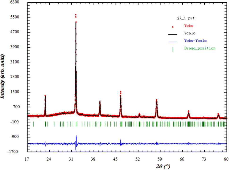 | ||
| Fig. 1 X-ray diffraction data and Rietveld refinements for 0.7(Na0.5Bi0.5)TiO3–0.3Bi0.7Sm0.3FeO3. | ||
A typical Rietveld refinement analysis of the sample is portrayed in Fig. 1. The results of the refinement of the structural parameters of our sample are as follows: a = 2.224 Å, b = 3.142 Å, c = 5.147 Å.
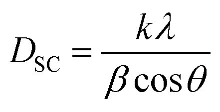
Using the X-ray diffraction (XRD) pattern, the size of the crystallites was determined in the case of Scherrer and that of Williamson–Hall (W–H). The average crystallite size was calculated from the full width at the half maximum (FWHM) of the most intense peak by using the Debye–Scherrer equation:31
 | (1) |
The Williamson–Hall equation takes into consideration all diffraction peaks and assumes their broadening, which is related to the crystalline size and the lattice strain. This is not considered in the Scherrer equation. Thus, X-ray line broadening is the sum of contributions of small crystallite size (βsize) and the broadening results from lattice strain (βstrain) in the system:
| β = βsize + βstrain | (2) |
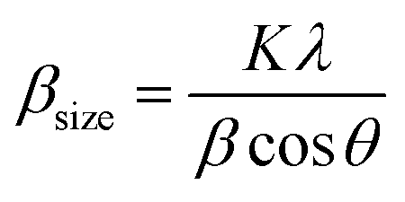 (Scherrer formula) and βstrain = 4εtanθ. We obtain the following equation:
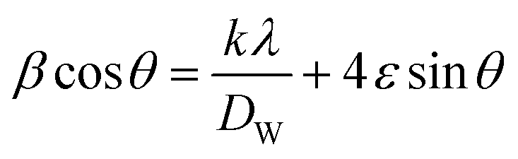 | (3) |
So
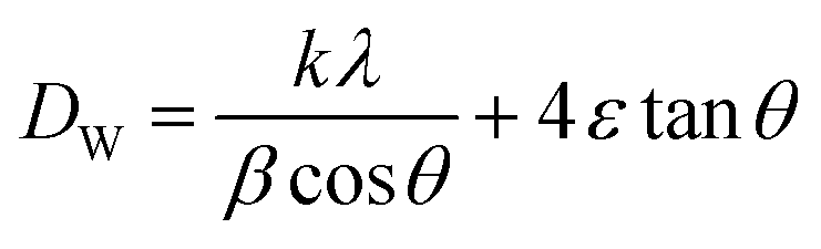 | (4) |
The Williamson–Hall (W–H) plots are displayed in Fig. 2. This plot provides a linear relationship between βcosθ and 4sinθ, whereas the slope provides the induced strain (ε = 1.25 × 10⁻³). The size of the crystallites (DW–H) was examined departing from the intercept of the line with the y-axis. It is noticeable that the straight-line intercepts all the points, indicating a uniform particle size distribution of the crystallites and a very low deformation. The calculated values of average crystallite size DSC and DW–H are outlined in Table 1. The DW–H value calculated using the Williamson–Hall method is higher than the one obtained using the Scherrer equation DSC.
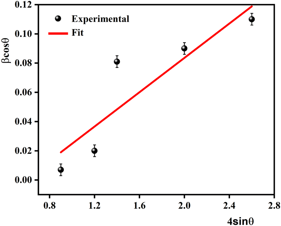 | ||
| Fig. 2 The Williamson–Hall plots for 0.7(Na0.5Bi0.5)TiO3–0.3Bi0.7Sm0.3FeO3. | ||
| Average crystallite size (nm) (Scherrer method) | DSC | 36 |
| Average of crystallite size (nm) (Williamson–Hall method) | DW–H | 54 |
| Particle size (μm) | DSEM | 1.25 |
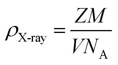
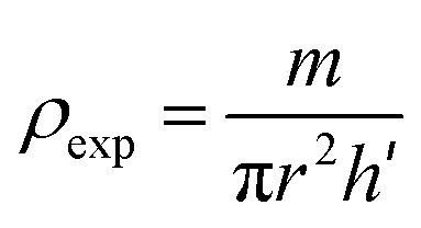
ρX-ray is the X-ray density that was calculated taking into consideration that a basic unit cell of the perovskite structure contains 8 ions according to the following formula:32
 | (5) |
 | (6) |
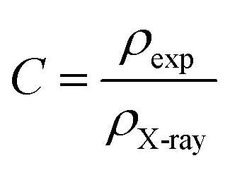
The compacity was specified according to the formula:34
 | (7) |
The notion of porosity is attributed to the difference between one and the compacity according to the following formula:35
| P(%) = (1 − C) × 100 | (8) |
The different parameters, such as bulk density ρexp, X-ray density ρX-ray, C compacity, and porosity P values, were calculated to obtain 3.653 g cm−3, 3.987 g cm−3, 0.913, and 8.7 (%), respectively.
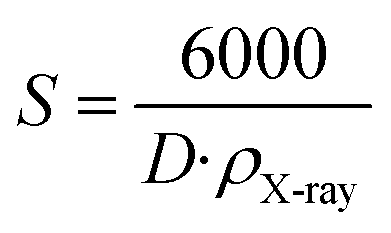
Assuming that all the particles are spherical, the specific surface area was determined using the following relation:36
 | (9) |
2.2. Morphological study
A scanning electron microscopy (SEM) analysis was performed to examine the surface morphology of this material. In Fig. 3, the SEM images exhibited in Fig. 3 reveal a microstructure with an almost homogeneous granular distribution and indicate that the morphology changes with doping.38 One can observe that the undoped sample (BiFeO3) is more compact in terms of agglomeration.39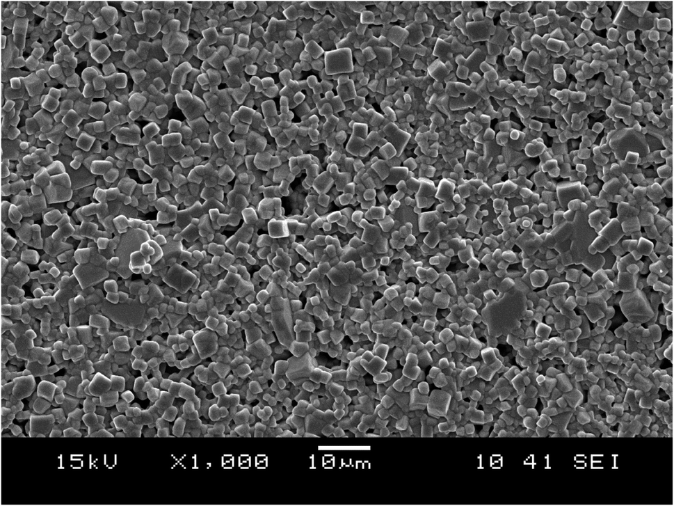 | ||
| Fig. 3 The SEM image for 0.7(Na0.5Bi0.5)TiO3–0.3Bi0.7Sm0.3FeO3. | ||
The micrograph displayed in Fig. 3 illustrates an interesting surface morphology of 0.7(Na0.5Bi0.5)TiO3–0.3Bi0.7Sm0.3FeO3. Scanning electron microscopy reveals a high melting or accumulation microstructure with polygonal and polyhedron-shaped grains. The average grain size of the particles (DSEM) is deduced by fitting the histogram (Fig. 4) by employing the image analyzer software ImageJ. DSEM which is ∼1.25 μm. This suggests that the grains have a polycrystalline structure, compared to the low crystallite size obtained from the XRD study.
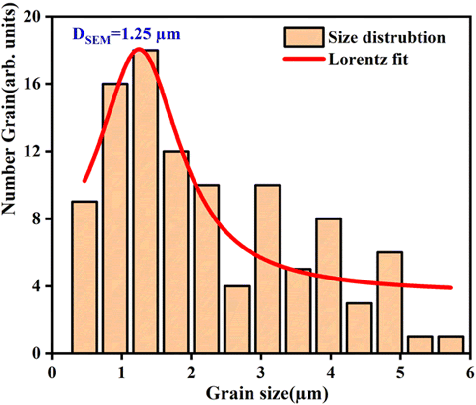 | ||
| Fig. 4 The histograms of the grain size distribution. | ||
2.3. Electrical study
The impedance plots of the ceramics can have one or more semicircles. Notably, in ceramics, the grain boundaries are highly resistive owing to the presence of a higher density of structural and chemical defects compared to grain interiors. Therefore, at high frequencies, the appearance of a smaller diameter semicircle is assigned to grain interiors, and a larger diameter semicircle is ascribed to grain boundaries.40,41 Nyquist plots as a function of frequency at different temperatures, of the studied compound are illustrated in Fig. 5. The Cole–Cole plots are characterized by the appearance of semicircles whose diameter decreases with the increase of temperature. The diameter of the semi-circle is related to the resistance of the compound. The increase in temperature reduces the diameter of the semicircle, indicating that the conduction process is thermally activated and therefore the sample is a semiconductor.42 The presence of a single semicircular arc implies a single relaxation phenomenon. The Cole–Cole plots are adjusted using the Z-view software,43 with combinations of the equivalent circuit models presented in Fig. 5. The appropriate fit was achieved through the use of an equivalent circuit, consisting of a combination series of two circuits: grain (R1–C1) and grain boundaries (R2–C2–CPE2), where R is the resistance and CPE is the constant phase element referring to the complex element.44 The presence of both relaxation phenomena (two circuits) in the Nyquist impedance plots can be attributed to the inhomogeneous distribution of oxygen. The values of all fitted parameters are presented in Table 2. In this respect, the good agreement between the theoretical background and experimental findings confirms the contribution of the grains and the grain boundary effects. | ||
| Fig. 5 Samples of the impedance plan plots. The inset shows the electrical equivalent circuit and the spectra of impedance from 723 to 803 K. | ||
| T(K) | R1 (Ω) | Q1 | α1 | R2 | Q2 | α2 | C2 |
|---|---|---|---|---|---|---|---|
| 623 | 28326 |
1,0973 × 10⁻⁸ | 0.84914 | 1.5798 × 10⁶ | 3.863 × 10⁻⁹ | 0.62872 | 3.897 × 10⁻¹⁰ |
| 643 | 25284 |
5.6958 × 10⁻⁹ | 0.86702 | 7.2857 × 10⁵ | 2.8531 × 10⁻⁹ | 0.68305 | 3.99668 × 10⁻¹⁰ |
| 663 | 22047 |
5.58 × 10⁻⁹ | 0.86876 | 3.4297 × 10⁵ | 4.408 × 10⁻⁹ | 0.6799 | 4.989 × 10⁻¹⁰ |
| 683 | 15007 |
1.069 × 10⁻⁸ | 0.82985 | 1.4339 × 10⁶ | 3.2752 × 10⁻⁹ | 0.75795 | 3.499 × 10⁻¹⁰ |
| 703 | 11578 |
5.094 × 10⁻⁹ | 0.8562 | 85890 |
2.599 × 10⁻⁸ | 0.49974 | 5.799 × 10⁻¹⁰ |
| 723 | 8968 | 6.5927 × 10⁻⁹ | 0.81999 | 87076 |
7.5908 × 10⁻⁸ | 0.4298 | 6.309 × 10⁻¹⁰ |
| 743 | 7163 | 5.223 × 10⁻⁹ | 0.80822 | 26286 |
4.9993 × 10⁻⁷ | 0.29344 | 3.442 × 10⁻¹⁰ |
| 763 | 5091 | 7.032 × 10⁻⁹ | 0.7794 | 15769 |
1.2459 × 10⁻⁶ | 0.2602 | 3.1 × 10⁻¹⁰ |
| 783 | 1517 | 8.782 × 10⁻⁸ | 0.67279 | 10529 |
1.293 × 10⁻⁶ | 0.29291 | 3.338 × 10⁻¹⁰ |
| 803 | 2280 | 3.0762 × 10⁻⁸ | 0.73221 | 11315 |
2.2064 × 10⁻⁶ | 0.24041 | 3.8791 × 10⁻¹⁰ |
On the other hand, we notice that the values of R2 are larger than those of R1, which can be attributed to a disorder of the atomic arrangement near the region of the grain boundaries, and accordingly, it causes an increase in the diffusion of the electrons.
The activation energy can be computed using the Arrhenius law:45
 | (10) |
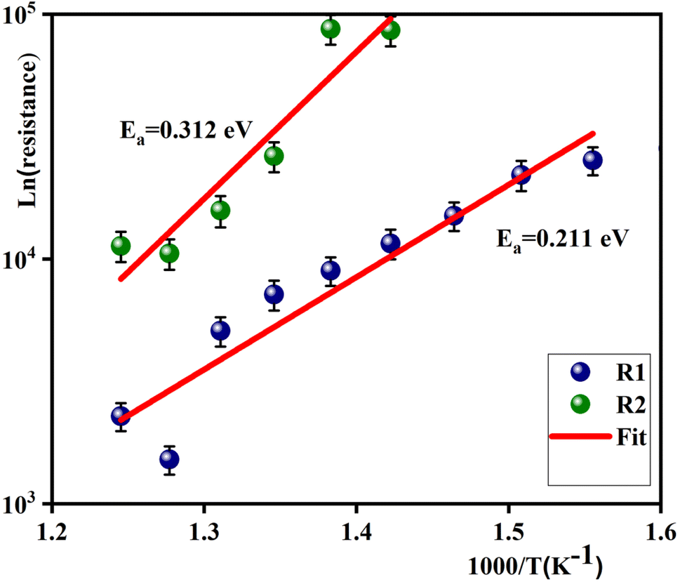 | ||
| Fig. 6 Arrhenius plots showing the dependence resistance of grain boundaries (R1) and grains (R2) versus 1000/T for 0.7(Na0.5Bi0.5)TiO3–0.3Bi0.7Sm0.3FeO3. | ||
Fig. 7(a) and (b) illustrate the variation of the real and imaginary parts ε′ (ω) and ε′′ (ω) with frequency on a double logarithmic scale at different temperatures. It can be detected from Fig. 7 that the ε′ exponentially decreases with increasing frequency and reaches almost a constant value at higher frequencies; which can be associated with the polar nature of the host matrix. There is adequate time for the dipoles to position themselves in the electric field at low frequencies before changing their direction; as they rise, the dielectric loss value.46 Conversely, when the frequency becomes high, the dipoles cannot follow up the too-rapid variations of the electric field, which reduces the dielectric loss value. This result corroborates the lossless nature of the samples at higher frequencies. The higher value of ε′ in the low-frequency region may be ascribed to the presence of mobile charges inside the ceramics backbone.47
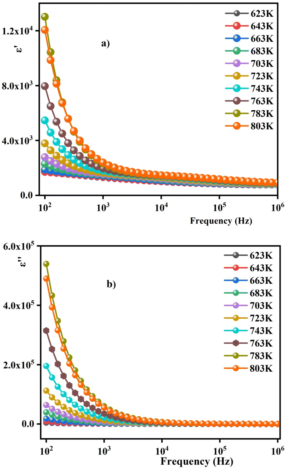 | ||
| Fig. 7 (a) Frequency-dependent real part (ε′) and (b) imaginary part (ε′′) of the dielectric constant measured at different temperatures for 0.7(Na0.5Bi0.5)TiO3–0.3Bi0.7Sm0.3FeO3. | ||
Fig. 8 foregrounds the complex modulus spectrum (M′′ vs. M′) of the sample at different temperatures. The appearance of an arc in the spectrum confirms the single-phase character of the material. This goes in good accordance with the observations drawn from XRD, which may be attributed to the presence of electrical relaxation phenomena.
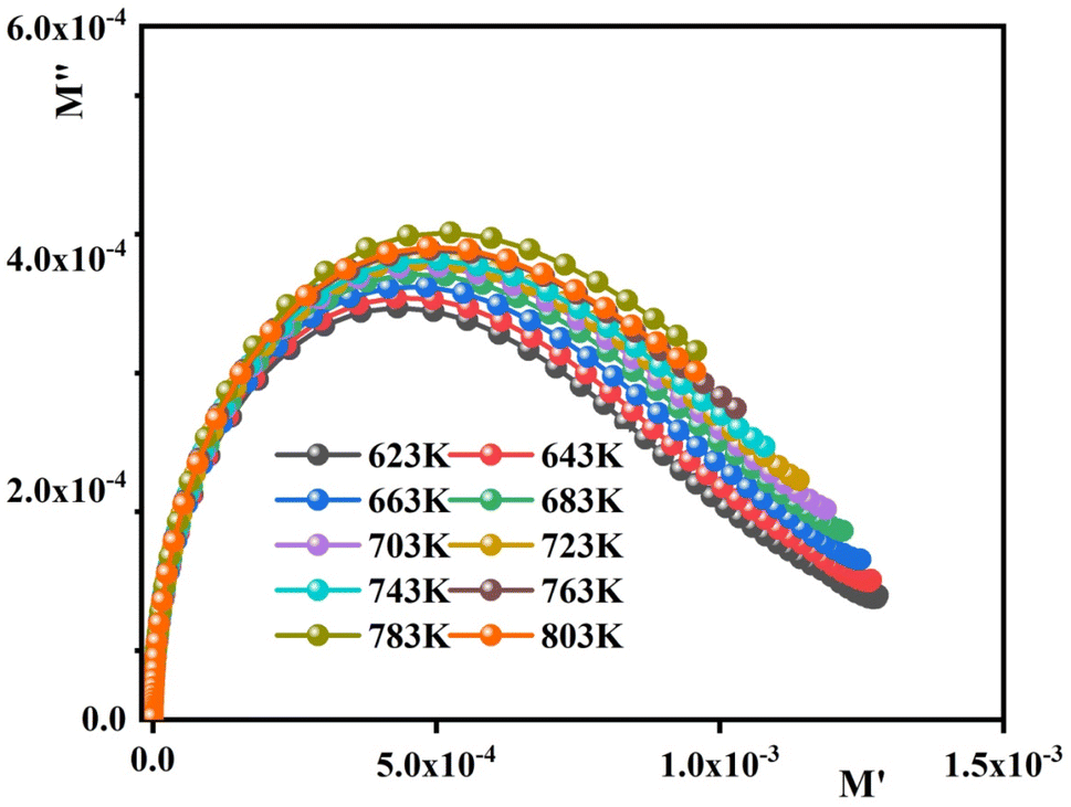 | ||
| Fig. 8 Complex modulus spectrum of the material at different temperatures. | ||
The variation of the imaginary part of modulus (M′′) as a function of frequency at various temperatures is plotted in Fig. 9. Departing from the graph, it is clear that (M′′) typically exhibits a well-defined maximum to which a characteristic relaxation rate can be associated and also displays asymmetric frequency dependence. The charge carriers may be considered mobile over long distances at lower frequencies lying to the left of the peaks. The frequency region below the maximum peak determines the range in which charge carriers are mobile on long-range distances, and above the maximum peak, the carriers are confined to potential wells being mobile on short distances. This region of the peak is therefore indicative of the transition from long-range dominated to short-range dominated mobility.48 In addition, the shifting of the peak frequencies in the higher frequency region with temperature implies that the relaxation time decreases with increasing temperature.
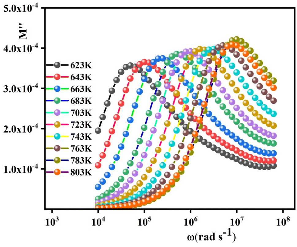 | ||
| Fig. 9 The imaginary part of the electric modulus as a function of frequency for 0.7(Na0.5Bi0.5)TiO3–0.3Bi0.7Sm0.3FeO3. | ||
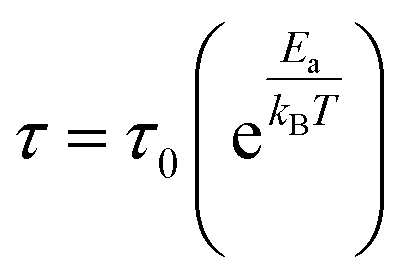
On the other hand, to determine the activation energy Ea of the relaxation process in the studied sample, the thermal evolution of the relaxation time τ is traced in Fig. 10. The latter is related to the relaxation frequency fmax of the maximum of each peak, by 2πτfmax = 1. The obtained plot abides by the following Arrhenius law:49
 | (11) |
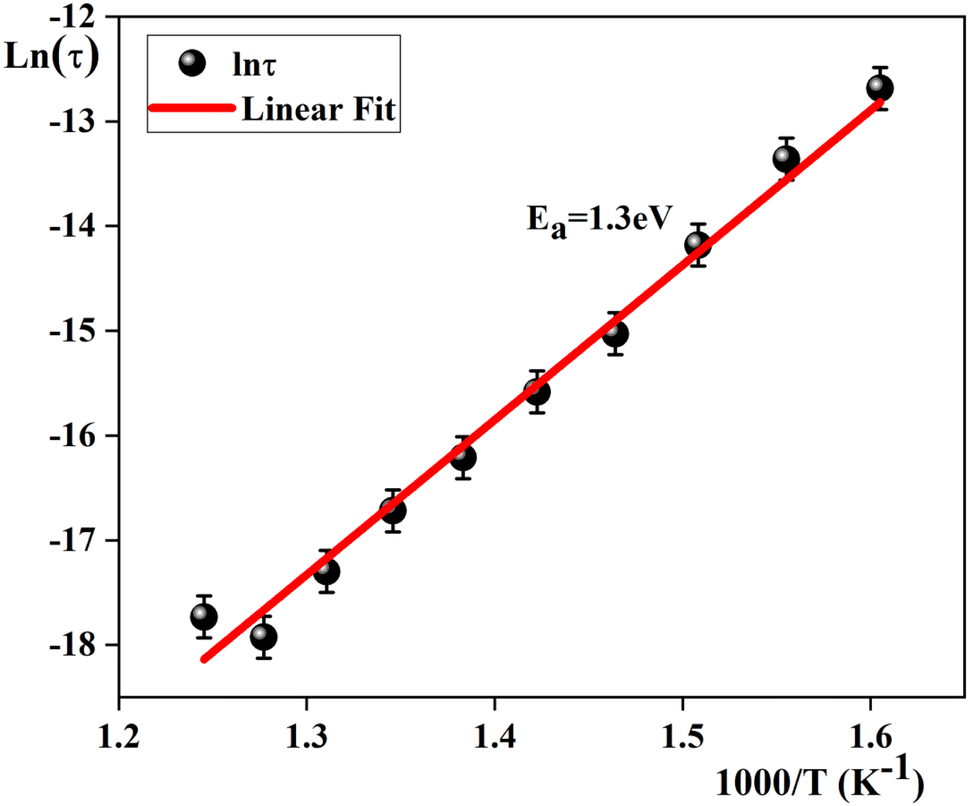 | ||
| Fig. 10 Variation in ln(τ) versus 1000/T. | ||
To gain a deeper insight into electrical behavior and determine the nature of conduction as well as the parameters controlling this process, the variation of the ac conductivity as a function of frequency is represented in Fig. 11. These spectra demonstrate that the conductivity increases with the increase in temperature. At the lower frequencies (102–104 Hz), the conductivity spectra display nearly constant values (σdc) as the random distribution of the charge carriers gives rise to frequency-independent conductivity. DC conductivity is thermally activated, which can exhibit the semiconductor behavior by the leap of the localized load carrier.51 The semiconductor nature indicates that this compound can be promising in certain applications such as optoelectronics, photodetectors, and photovoltaics.52–54 With increasing frequencies, the σac shows a dispersion that moves towards the higher frequencies with the increase in temperature. The conductivity spectra are identified by Jonscher's universal power law in the form of:55
| σ(ω) = σdc + σac = σdc + AωS | (12) |
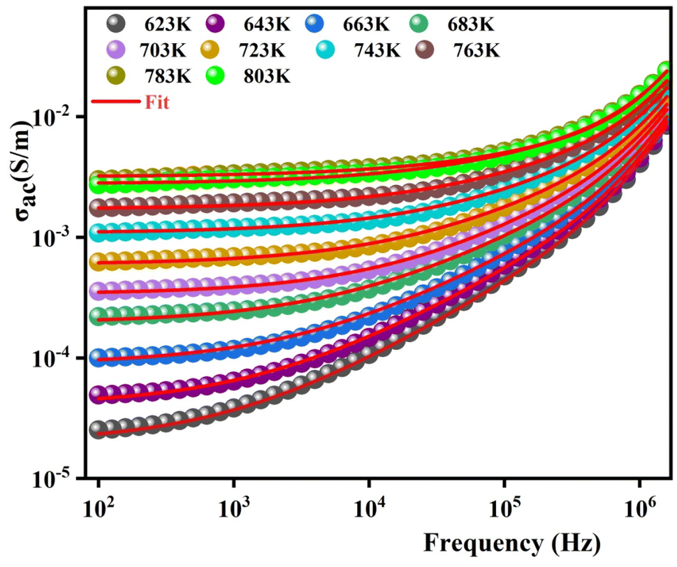 | ||
| Fig. 11 The variation in the electrical conductivity versus the frequency at different temperatures for 0.7(Na0.5Bi0.5)TiO3–0.3Bi0.7Sm0.3FeO3. | ||
The results of fitting are summarized in Fig. 12. A good consistency between experimental and theoretical data is noted.
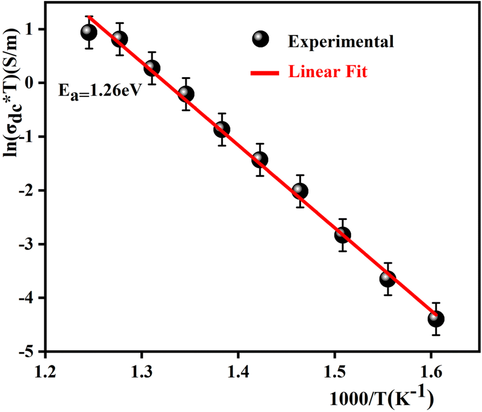 | ||
| Fig. 12 The variation in ln(σdc × T) versus 1000/T for 0.7(Na0.5Bi0.5)TiO3–0.3Bi0.7Sm0.3FeO3. | ||
The logarithmic variation of dc conductivity as a function of the inverse of temperature is depicted in Fig. 13. This variation can be described by the Arrhenius equation as:56
 | (13) |
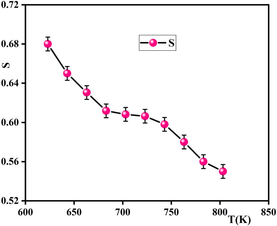 | ||
| Fig. 13 Temperature dependence of the exponent s for the sample. | ||
The exponent ‘‘S,’’ which represents the degree of interaction between ions and their surroundings, represents an outstanding source of information about the model for the conduction mechanism in the material from which it is clear that s declines with the decrease of temperature (Fig. 13). This indicates that the Correlated Barrier Hopping (CBH) model is suitable to explain the conduction process. Based on the CBH model, the frequency exponent s is computed as:57
 | (14) |
2.4. Dielectric study
Dielectric measurements were carried out as a function of temperature and frequency to investigate their dielectric behavior by determining the ferroelectric phase transition temperature and the nature of the relaxing ferroelectric behavior of the perovskite.Fig. 14(a) illustrates the variation of the real part of dielectric permittivity (ε′) as a function of temperature at different frequencies for 0.7(Na0.5Bi0.5)TiO3–0.3Bi0.7Sm0.3FeO3 ceramics. The ε′ values increase gradually with the increase in temperature and frequency, respectively. This refers basically to the intrinsic behavior of BiFeO3's bulk. Up to 320 K, the dielectric permittivity gradually increases as the temperature rises. This behavior can be assigned to orientational polarization where dipoles align themselves along the electric field direction and fully contribute to the total polarization.58 As the temperature rises above 350 K, permittivity starts to increase abnormally referring to the ferroelectric–paraelectric transition. The fluctuation of the dielectric constant as a function of temperature suggests the existence of a peak at a specific temperature (Tmax), confirming that the dielectric constant has a relaxor thermal evolution. The relaxor behavior is triggered by homovalent and heterovalent substitutions at sites A and B for the studied ceramics and the composition fluctuation gives rise to the relaxing behavior, favoring the strong heterogeneity. Furthermore, the creation of the Coulomb interactions at long distances prevents the formation of ferroelectric microdomains in favor of the formation of the polar nanoregions PNRs.59 Similar observations were reported with other ceramics.60
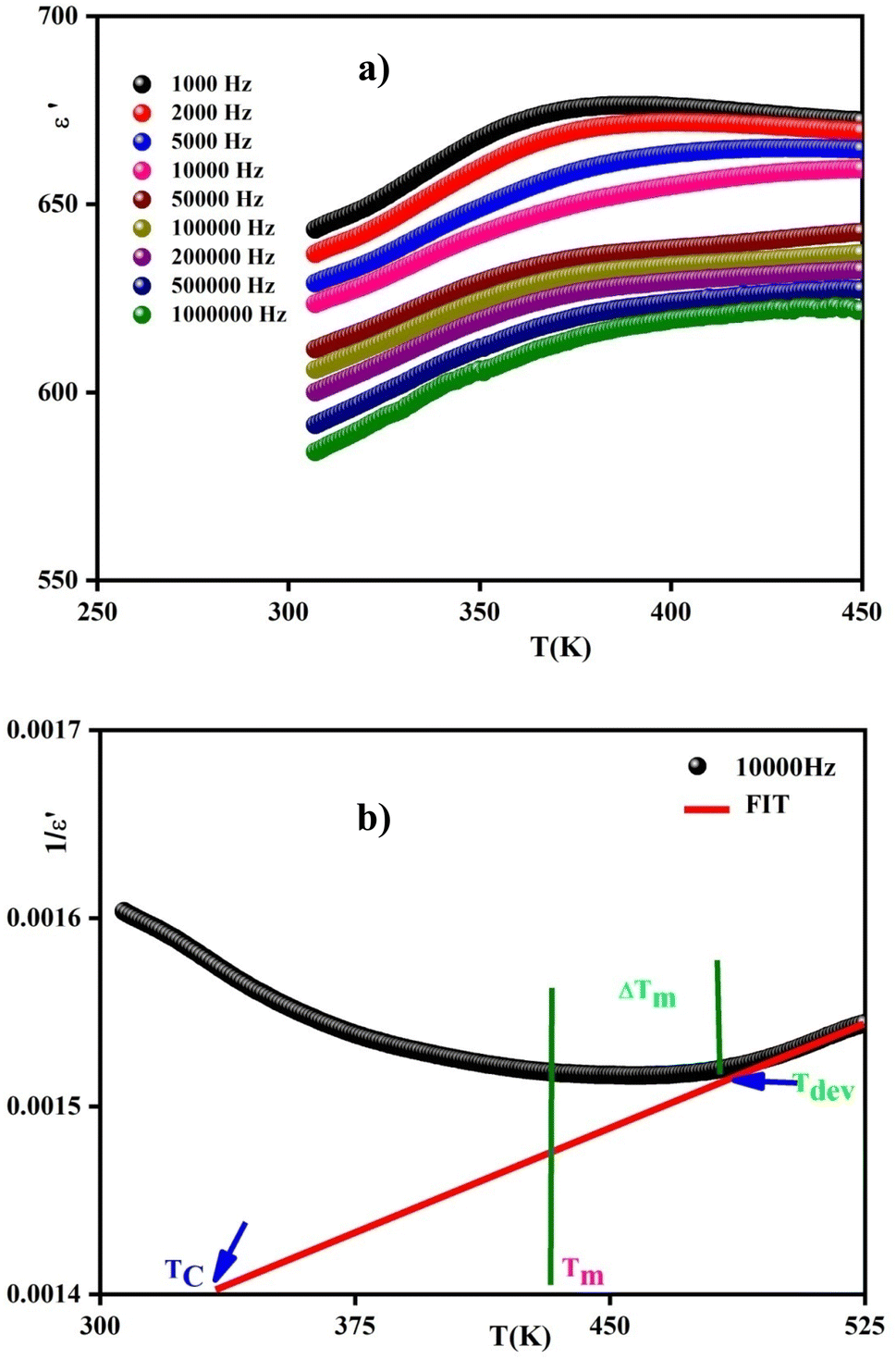 | ||
Fig. 14 (a) Thermal variation in permittivity  for 0.7(Na0.5Bi0.5)TiO3–0.3Bi0.7Sm0.3FeO3 (b) Thermal variation in the inverse of the real part of the permittivity for 0.7(Na0.5Bi0.5)TiO3–0.3Bi0.7Sm0.3FeO3 (b) Thermal variation in the inverse of the real part of the permittivity  at 1 kHz, for 0.7(Na0.5Bi0.5)TiO3–0.3Bi0.7Sm0.3FeO3. at 1 kHz, for 0.7(Na0.5Bi0.5)TiO3–0.3Bi0.7Sm0.3FeO3. | ||
Moreover, the values of ε′ for the doped system proved to be higher than BiFeO3, which can be ascribed to the homovalent and heterovalent substitutions at sites A and B for the studied ceramics. These substitutions enhance the polarisability effect and consequently increase the polarisation in the doped BiFeO3 materials.61 In comparison with other similar ceramics, we notice that the insertion of the dopant ions entails an increase in permittivity of the ceramics (Table 3) owing to the enhancement of polarisation in the doped materials.62–64
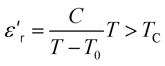
The thermal variation of 1/ε′ of this compound is presented in Fig. 14(b), demonstrating a deviation from the Curie–Weiss law provided by the equation:65
 | (15) |
Further theoretical fitting reveals that the transition is diffuse in this case and that the behavior is of the relaxor type. This is a second-order transition, where C is the Curie–Weiss constant and TC is the Curie–Weiss temperature. Since ion diffusion occurs with increasing temperature, the movement of TC (i.e., the transition from the antiferroelectric to the paraelectric state) at high temperatures is most likely due to space charge polarization.66
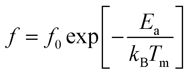
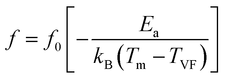
It is noteworthy that the evolution of the maximum peak temperature of permittivity depending on frequency was analyzed using two theoretical models, namely the Debye law and Vogel–Fulcher (V–F). Dipoles can rotate and are thermally activated in Debye relaxation. The moments of the dipoles are the same, and there is no interaction between them. The Debye model is expressed in terms of:67
 | (16) |
 | (17) |
 | ||
| Fig. 15 Fitting the dielectric relaxation data of the sample of (a) Debye and (b) Vogel–Fulcher model. | ||
3. Conclusion
The effect of Na, Ti, and Sm on the structural, dielectric, and electric properties and the temperature of the phase transition of BiFeO3 was explored, investigated, and discussed.Unit cell parameters at room temperature for all studied compounds were determined. It was demonstrated that Na, Ti, and Sm substitutions, tend to stabilize the orthorhombic structure.
SEM micrographs revealed the appearance of particles of unequal size. The ac conductivity proved to meet the universal power law. The Z′′ and M′′ spectra indicated the scaling behavior. The thermally activated process variation with temperature and frequency was explained based on the CBH model. The behavior of the dielectric constant observed in this sample proved to be a typical ferroelectric-paraelectric phase transition with relaxor-like behavior. As a final note, it is noteworthy that the obtained results can be regarded as valuable and worthwhile as they suggest that bismuth-doped nanocrystalline 0.7(Na0.5Bi0.5)TiO3–0.3(Bi0.7Sm0.3)FeO3 can be a promising room-temperature multiferroic material for memory devices. Indeed, the sample has a high dielectric constant, a low loss tangent, and a high TC, and can therefore the considered an outstanding material for multifunctional devices.
Conflicts of interest
The authors declare that they have no conflict of interests.Acknowledgements
The researchers would like to acknowledge the Deanship of Scientific Research, Taif University for funding this work.References
- J. Wu, Z. Fan, D. Xiao, J. Zhu and J. Wang, Prog. Mater. Sci., 2016, 84, 335–402 CrossRef CAS.
- G. Catalan and J. F. Scott, Adv. Mater., 2009, 21, 2463–2485 CrossRef CAS.
- H. Tao, J. Lv, R. Zhang, R. Xiang and J. Wu, Mater. Des., 2017, 120, 83–89 CrossRef CAS.
- C. H. Yang, D. Kan, I. Takeuchi, V. Nagarajan and J. Seidel, Phys. Chem. Chem. Phys., 2012, 14, 15953 RSC.
- P. Uniyal and K. L. Yadav, Mater. Lett., 2008, 62, 2858–2861 CrossRef CAS.
- J. Wu, Z. Fan, D. Xiao, J. Zhu and J. Wang, Prog. Mater. Sci., 2016, 84, 335–402 CrossRef CAS.
- S.-T. Zhang, Y. Zhang, M.-H. Lu, C.-L. Du, Y.-F. Chen, Z.-G. Liu, Y.-Y. Zhu, N.-B. Ming and X. Q. Pan, Appl. Phys. Lett., 2006, 88(16), 162901 CrossRef.
- Z. Chai, G. Tan, Z. Yue, W. Yang, M. Guo, H. Ren, A. Xia, M. Xue, Y. Liu, L. Lv and Y. Liu, J. Alloys Compd., 2018, 746, 677–687 CrossRef CAS.
- J.-H. Zhu, J.-Q. Dai, J.-W. Xu and X.-Y. Li, Ceram. Int., 2018, 44, 9215–9220 CrossRef CAS.
- C. Yu, G. Viola, D. Zhang, K. Zhou, V. Koval, A. Mahajan, R. M. Wilson, N. V. Tarakina, I. Abrahams and H. Yan, J. Eur. Ceram. Soc., 2018, 38, 1374–1380 CrossRef CAS.
- X. Zhang, Y. Sui, X. Wang, Y. Wang and Z. Wang, J. Alloys Compd., 2010, 507(1), 157–161 CrossRef CAS.
- D. V. Thang, N. M. Hung, D. T. X. Thao, L. T. M. Oanh, D. D. Bich, N. C. Khang, V. Q. Nguyen and N. Van Minh, IEEE Magn. Lett., 2019, 10, 1–5 Search PubMed.
- X. Yan, G. Tan, W. Liu, H. Ren and A. Xia, Ceram. Int., 2015, 41(2), 3202–3207 CrossRef CAS.
- K. Chakrabarti, K. Das, B. Sarkar, S. Ghosh, S. K. De, G. Sinha and J. Lahtinen, Appl. Phys. Lett., 2012, 101, 042401 CrossRef.
- X. Xu, T. Guoqiang, R. Huijun and X. Ao, Ceram. Int., 2013, 39, 6223–6228 CrossRef CAS.
- L. Yu, H. Deng, W. Zhou, Q. Zhang, P. Yang and J. Chu, Mater. Lett., 2016, 170, 85–88 CrossRef CAS.
- D. Gaspar, L. Pereira, A. Delattre, D. Guerin, E. Fortunato and R. Martins, Phys. Status Solidi C, 2015, 12(12), 1 Search PubMed.
- M. Zhang, X. Zhang, X. Qi, Y. Li, L. Bao and Y. Gu, Ceram. Int., 2017, 43(18), 16957–16964 CrossRef CAS.
- R. S. N. Ain, S. A. Halim and M. Hashim, Adv. Mater. Res., 2012, 501, 329–333 CAS.
- H. Singh and K. L. Yadav, Ceram. Int., 2015, 41(8), 9285–9295 CrossRef CAS.
- X. F. Wu, G. A. Zhang and F. F. Wu, Bull. Mater. Sci., 2016, 39(3), 703–709 CrossRef CAS.
- C. Gumiel, T. Jardiel, M. S. Bernardo, P. G. Villanueva, U. Urdiroz, F. Cebollada, C. Aragó, A. C. Caballero and M. Peiteado, Ceram. Int., 2019, 45(5), 5276–5283 CrossRef CAS.
- M. Mahesh Kumar, K. Srinivas and S. V. Suryanarayana, Appl. Phys. Lett., 2000, 76(10), 1330–1332 CrossRef CAS.
- Reetu, A. Agarwal, S. Sanghi and Ashima, J. Appl. Phys., 2011, 110, 073909 CrossRef.
- P. Kumar and M. Kar, J. Alloys Compd., 2014, 584, 566–572 CrossRef CAS.
- T. D. Rao, T. Karthik and S. Asthana, J. Rare Earths, 2013, 31, 370–375 CrossRef CAS.
- M. Hasan, M. A. Hakim, M. A. Basith, M. S. Hossain, B. Ahmmad, M. A. Zubair, A. Hussain and M. F. Islam, AIP Adv., 2016, 6, 035314 CrossRef.
- M. M. Rhaman, M. A. Matin, M. A. Hakim and M. F. Islam, Mater. Res. Express, 2019, 6, 1–22 Search PubMed.
- Z. Hu, M. Li, J. Liu, L. Pei, J. Wang, B. Yu and X. Zhao, J. Am. Ceram. Soc., 2010, 93(9), 2743–2747 CrossRef CAS.
- C.-J. Cheng, D. Kan, S.-H. Lim, W. R. McKenzie, P. R. Munroe, L. G. Salamanca-Riba, R. L. Withers, I. Takeuchi and V. Nagarajan, Phys. Rev. B: Condens. Matter Mater. Phys., 2009, 80, 014109 CrossRef.
- L. Yu, H. Deng, W. Zhou, Q. Zhang, P. Yang and J. Chu, Mater. Lett., 2016, 170, 85–88 CrossRef CAS.
- V. Dillu, M. T. Kebede, S. Devi and S. Chauhan, Mater. Today: Proc., 2021, 34, 813–816 CAS.
- D. P. Dutta, O. D. Jayakumar, A. K. Tyagi, K. G. Girija, C. G. S. Pillai and G. Sharma, Nanoscale, 2010, 2, 1149–1154 RSC.
- D. P. Dutta and A. K. Tyagi, Appl. Surf. Sci., 2018, 450, 429–440 CrossRef CAS.
- W. Eerenstein, N. D. Mathur and J. F. Scott, Nature, 2006, 442, 759–765 CrossRef CAS PubMed.
- S. Kitagawa, T. Ozaki, Y. Horibe, K. Yoshii and S. Mori, Ferroelectrics, 2008, 376(1), 122–128 CrossRef CAS.
- F. Akram, J. Kim, S. A. Khan, A. Zeb, H. G. Yeo, Y. S. Sung, T. K. Song, M.-H. Kim and S. Lee, J. Alloys Compd., 2020, 818(152878), 1–38 Search PubMed.
- B. Yotburut, P. Thongbai, T. Yamwong and S. Maensiri, Ceram. Int., 2017, 43, 5616–5627 CrossRef CAS.
- J. Lv, J. Wu and W. Wu, J. Phys. Chem. C, 2015, 119, 21105–21115 CrossRef CAS.
- Reetu, A. Agarwal, S. Sanghi, Ashima and N. Ahlawat, J. Phys. D: Appl. Phys., 2012, 45(165001), 1–10 Search PubMed.
- G. Catalan and J. F. Scott, Adv. Mater., 2009, 21, 2463–2485 CrossRef CAS.
- A. Chaudhuri and K. Mandal, Mater. Res. Bull., 2012, 47, 1057–1061 CrossRef CAS.
- S. K. Singh, H. Ishiwara, K. Sato and K. Maruyama, J. Appl. Phys., 2007, 102, 094109 CrossRef.
- C.-H. Yang, D. Kan, I. Takeuchi, V. Nagarajan and J. Seidel, Phys. Chem. Chem. Phys., 2012, 14, 15953–15962 RSC.
- D. Lin, Q. Zheng, Y. Li, Y. Wan, Q. Li and W. Zhou, J. Eur. Ceram. Soc., 2013, 33, 3023–3036 CrossRef CAS.
- C. Elissalde and J. Ravez, J. Mater. Chem., 2001, 11, 1957–1967 RSC.
- H. Naganuma, J. Miura and S. Okamura, Appl. Phys. Lett., 2008, 93, 052901 CrossRef.
- D. Viet Thang, L. Thi Mai Oanh, N. Cao Khang, N. Manh Hung, D. Danh Bich, D. Thi Xuan Thao and N. Van Minh, AIMS Mater. Sci., 2017, 4, 982–990 Search PubMed.
- S. Dabas, M. Kumar and O. P. Thakur, Ceram. Int., 2020, 46(11), 17361–17375 CrossRef CAS.
- S. Pattanayak, B. N. Parida, P. R. Das and R. N. P. Choudhary, Appl. Phys. A, 2012, 112(2), 387–395 CrossRef.
- S. Pattanayak, R. N. P. Choudhary, P. R. Das and S. R. Shannigrahi, Ceram. Int., 2014, 40(6), 7983–7991 CrossRef CAS.
- R. K. Mishra, D. K. Pradhan, R. N. P. Choudhary and A. Banerjee, J. Phys.: Condens. Matter, 2008, 20(4), 1–6 CrossRef.
- E. Dul’kin, S. Kojima and M. Roth, J. Appl. Phys., 2011, 110(4), 044106 CrossRef.
- C. M. Zhu, G. B. Yu, L. G. Wang, M. W. Yao, F. C. Liu and W. J. Kong, J. Magn. Magn. Mater., 2020, 506(166803), 1–5 Search PubMed.
- F. D. Morrison, D. C. Sinclair and A. R. West, J. Appl. Phys., 1999, 86(11), 6355–6366 CrossRef CAS.
- G. Singh, V. S. Tiwari and P. K. Gupta, J. Appl. Phys., 2010, 107(6), 064103 CrossRef.
- S. Steinsvik, R. Bugge, J. Gjonnes, J. Tafto and T. Norby, J. Phys. Chem. Solids, 1997, 58(6), 969–976 CrossRef CAS.
- N. Kumar, A. Dutta, S. Prasad and T. P. Sinha, Phys. B, 2010, 405(21), 4413–4417 CrossRef CAS.
- K. P. F. Siqueira, R. L. Moreira and A. Dias, Chem. Mater., 2010, 22(8), 2668–2674 CrossRef CAS.
- O. Polat, M. Coskun, F. M. Coskun, Z. Durmus, M. Caglar and A. Turut, J. Mater. Sci.: Mater. Electron., 2018, 29(19), 16939–16955 CrossRef CAS.
- M. Enneffati, B. Louati, K. Guidara, M. Rasheed and R. Barillé, J. Mater. Sci.: Mater. Electron., 2017, 29(1), 171–179 CrossRef.
- Y. Moualhi, R. M’nassri, M. M. Nofal, H. Rahmouni, A. Selmi, M. Gassoumi, N. Chniba-Boudjada, K. Khirouni and A. Cheikhrouhou, J. Mater. Sci.: Mater. Electron., 2020, 31(23), 21046–21058 CrossRef CAS.
- I. Ouni, H. Ben Khlifa, R. M’nassri, M. M. Nofal, E. M. A. Dannoun, H. Rahmouni, K. Khirouni and A. Cheikhrouhou, Appl. Phys. A, 2021, 127(8), 1–12 CrossRef.
- L. Khemakhem, A. Kabadou, A. Maalej, A. B. Salah, A. Simon and M. Maglione, J. Alloys Compd., 2008, 452(2), 451–455 CrossRef CAS.
- S. Aydi, A. Amouri, S. Chkoundali and A. Aydi, Ceram. Int., 2017, 43(15), 12179–12185 CrossRef CAS.
- S. Chakrabarty, M. Pal and A. Dutta, Ceram. Int., 2018, 44(12), 14652–14659 CrossRef CAS.
- I. Soudani, K. Ben Brahim, A. Oueslati, H. Slimi, A. Aydi and K. Khirouni, RSC Adv., 2022, 12(29), 18697–18708 RSC.
- S. Wachowski, A. Mielewczyk-Gryń, K. Zagórski, C. Li, P. Jasiński, S. J. Skinner, R. Haugsrud and M. Gazda, J. Mater. Chem. A, 2016, 4(30), 11696–11707 RSC.
- A. Mielewczyk-Gryn, T. Lendze, K. Gdula-Kasica, P. Jasinski, A. Krupa, B. Kusz and M. Gazda, Open Phys., 2013, 11(2), 213–218 CAS.
- S. Aydi, S. Chkoundali, A. Oueslati and A. Aydi, Effect of lithium doping on the structural, conduction mechanism and dielectric property of MnNbO4, RSC Adv., 2023, 13, 20093–20104 RSC.
- A. Amouri, S. Aydi, N. Abdelmoula, H. Dammak and H. Khemakhem, J. Alloys Compd., 2018, 739, 1065–1079 CrossRef CAS.
| This journal is © The Royal Society of Chemistry 2024 |