 Open Access Article
Photonic post-processing of a multi-material transparent conductive electrode architecture for optoelectronic device integration†
Luis Felipe Gerlein ,
Jaime Alberto Benavides-Guerrero and
Sylvain G. Cloutier*
Department of Electrical Engineering, École de Technologie Supérieure, 1100 Notre-Dame Ouest, Montréal, Canada H3C 1K3. E-mail: SylvainG.Cloutier@etsmtl.ca
First published on 5th February 2024
Abstract
Emerging flexible optoelectronic devices require multi-material processing capabilities to fully enable the use of temperature-sensitive substrates and materials. This report demonstrates how photonic sintering enables the processing of materials with very different properties. For example, charge carrier transport/blocking metal-oxides, and transparent conductive silver nanowire-based electrodes ought to be compatible with low-energy and high-throughput processing for integration onto flexible low-temperature substrates. Compared to traditional post-processing methods, we show a rapid fabrication route yielding highly-stable hybrid electrode architectures on polyethylene terephthalate (PET). This architecture consists of an interconnected silver nanowire network encapsulated with a thin crystalline photo-sensitive titanium dioxide (TiO2) coating, allowing both layers to be treated using independent photonic post-processing sintering steps. The first step sinters the nanowires, while the second completes the conversion of the top metal-oxide layer from amorphous to crystalline TiO2. This approach improves on the fabrication speed compared to oven processing, while delivering optical and electrical characteristics comparable to the state of the art. Optimized transparency values reach 85% with haze values down-to 7% at 550 nm, while maintaining a sheet resistance of 18.1 Ω sq.−1. However, this hybrid architecture provides a much stronger resilience to degradation, which we demonstrate through exposure to harsh plasma conditions. In summary, this study shows how carefully-optimized photonic curing post-processing can provide more-stable hybrid architectures while using a multi-material processing technique suitable for high-volume manufacturing on low-temperature substrates.
1 Introduction
Flexible hybrid optoelectronic integration faces several fundamental challenges before achieving low-cost manufacturing of high-performance devices on low-temperature flexible substrates. These low-cost substrates generally bring stringent processing requirements, leading to critical manufacturing issues. Emerging techniques such as laser- or flash lamp-based (so-called photonic) post-processing sintering offer promising alternatives to conventional oven-based processing of heat-sensitive substrates.1–8 By carefully tuning the processing conditions for each individual material, it becomes possible to process multiple thin films independently on the same device, without thermal annealing and at high speeds. Thin films made of metallic nanoparticles need to be processed with a small number of high power density pulses to achieve high-density conductive films.9,10 For ceramic materials, a larger number of lower power-density pulses tends to achieve improved densification and crystallization.11 While these general rules may seem incompatible, they can be combined to process multi-material devices using the same rapid-processing equipment. Indeed, this possibility to process multiple materials using a minimal set of tools could prove a great advantage for the rapid assembly of flexible devices by reducing the number of fabrication steps and increasing their throughput.One important component of many flexible hybrid optoelectronic devices is the transparent conductive electrode (TCE). However, they can be especially difficult to integrate on low-temperature flexible substrates. Similarly, carrier transport/blocking metal-oxide layers also often require processing steps incompatible with low-temperature substrates. These common materials widely-used in optoelectronics were previously treated using photonic post-processing.3,4,12 However, combining them brings a whole new level of complexity for the processing technique to remain unchanged.
Percolated networks of silver nanowires are ideal candidates for indium-tin-oxide (ITO) film replacement due to higher conductivity,13–16 improved substrate adhesion,8,17 high optical transmission18–20 and flexibility.5,21 Photonic sintering of metallic nanowires can be successful in creating semitransparent, conductive percolated networks, because of the light-induced plasmonic welding that can occur at the nanowire junction.22,23 Most metallic nanostructures exhibit surface plasmon resonance throughout the visible spectrum, making them strong light absorbers compared to non-plasmonic nanoparticles.24 This is why photonic sintering systems rely on high-power and wide-spectrum xenon flash lamps.4
Meanwhile, emerging solution-based metal-oxide precursors offer a great potential for integration on low-temperature flexible substrates using high-throughput industrial manufacturing processes.25–27 Titanium dioxide (TiO2) is of particular interest for a wide range of optoelectronics devices, both as an active material and as an electron transport layer.28,29 For example, inkjet-printed UV photodetectors exploiting the synergistic relationship between TiO2 and silver nanowires have been demonstrated, highlighting the potential of these two materials for printed optoelectronic device development.28,30 Similarly, printed oxide thin-film transistors (TFTs) on memory polymers were also previously demonstrated.31 There, the metal-oxide layer is exposed to UV through shadow-masks in a roll-to-roll configuration. Ongoing research on large-area light-induced sintering & crystallization of metal-oxide materials such as titanium dioxide for optoelectronic devices can be divided into three main areas: UV source-induced,32–35 visible and NIR light-induced36–40 and broadband, pulsed light-induced crystallization.1,3,12,41,42 Traditionally, most metal oxides are transparent in the visible part of the spectrum, and photonic post-processing requires higher energy than that required to process metallic nanostructures.11
Previous reports describe hybrid composite architectures combining TiO2 and silver nanowires.17,43–46 These hybrid platforms have demonstrated improvements to the wire-to-wire junction resistance,17,44 the chemical stability of the network,45 the thermal resilience and overall electrode longevity when exposed to higher temperatures than those supported by bare nanowire networks.46,47 This is mainly achieved using conformal coatings through atomic layer deposition techniques or decorating the silver nanowires with metal-oxide nanoparticles.43,46 These improved operating conditions enabled the development of thin-film transistors on rigid substrates and flexible memristors.17,48 However, these current methods of deposition and treatment of the TiO2 layer still rely on amorphous metal-oxide films, traditional sol–gel chemical routes, use of rigid substrates, complicated and expensive and low-yield depositing techniques. Overall, these methods miss out on the potential advantages of using crystalline materials and the possibility for integration into streamlined roll-to-roll fabrication facilities.17,48
This report describes a simple fabrication method for producing a multi-material, stable hybrid TCE architecture on PET using two separate photonic post-processing treatment steps. The detailed processing conditions illustrate how to exploit the response of each material to tune the flashing parameters, allowing each material to be processed independently of the others. The use of photo-sensitive TiO2 not only provides important environmental protection and stability to these films, while further improves their electrical properties. These hybrid TCE architectures offer a platform that can be integrated into the fabrication of next-generation optoelectronic components at low fabrication costs by incorporating straightforward fabrication techniques.
2 Results
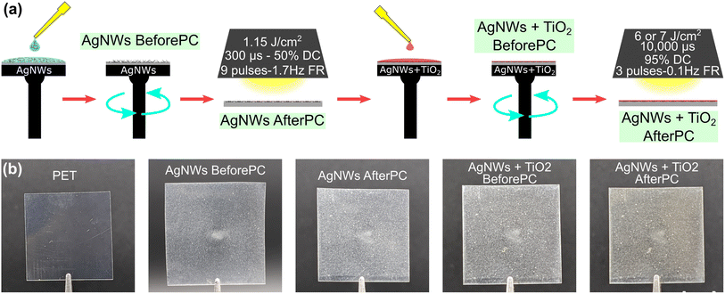
A step-by-step overview of the fabrication process for the hybrid TCEs is shown in Fig. 1, comparing the pristine and coated PET substrates. It is worth noting that the dark background greatly enhances the contrast of the images compared to a white background, but visually exaggerates the apparent loss of transparency and haze of the films, which will both be quantified later. The labels highlighted in green identify each processing step, and this nomenclature will be used throughout the manuscript. As explained in the Experimental section, plasma is used to clean and prepare the flexible PET substrates. For both layers, similar spin-coating conditions of 4000 rpm for 30 seconds are used for material deposition. Optimal photonic sintering parameters for the welding of the AgNWs atop the PET substrates are based on a previously-published study.5 A rapid succession of 9 pulses at a firing rate of 1.7 Hz, fluence of 1.15 J cm−2, an envelope of 300 μs with 50% pulse duty-cycle are enough to weld the silver nanowires, creating a highly conductive layer. In this stage, the pulse conditions and the number of pulses are optimized to achieve the best sheet resistance (Rsh) value for the TCE films, while preserving the bulk structural and optical properties of the PET. Photographs of samples at each fabrication stage are shown in Fig. 1(b).Subsequently, a solution consisting of a 10% w/w dilution of the photo-sensitive TiO2 in anhydrous ethanol was prepared and deposited by spin-coating. This photo-sensitive TiO2 precursor is synthesized following a previously-published procedure,37 which is also briefly summarized in the Experimental section. This special chemical route yields a defect-rich TiO2 sol–gel precursor, for which the visible-light absorption is significantly enhanced.49 This amorphous precursor is shown to crystallize using 405 or 532 nm laser sources, under environmental conditions.36–38 It is also suitable for photonic post-processing using a wide-spectrum light source such as a xenon flash lamp. This crystalline TiO2 layer can be used in the fabrication of optoelectronic devices, whether as the active layer of a photodetector or as an electron transport layer.30,44,45
The coated samples are then exposed a second time to crystallize the TiO2 layer using a slow progression of 3 pulses, delivered at a firing rate of 0.1 Hz, with an envelope of 10![[thin space (1/6-em)]](https://www.rsc.org/images/entities/char_2009.gif) 000 μs with a 95% duty cycle. The energy density delivered depends on the crystalline phase desired depending on the target application, using 6 J cm−2, or 0.6 kW cm−2, to convert to anatase. To crystallize into rutile, 7 J cm−2 or 0.7 kW cm−2, were necessary. This crystallized TiO2 layer provides increased protection of the nanowire-based electrode in this hybrid TCE architecture.
000 μs with a 95% duty cycle. The energy density delivered depends on the crystalline phase desired depending on the target application, using 6 J cm−2, or 0.6 kW cm−2, to convert to anatase. To crystallize into rutile, 7 J cm−2 or 0.7 kW cm−2, were necessary. This crystallized TiO2 layer provides increased protection of the nanowire-based electrode in this hybrid TCE architecture.
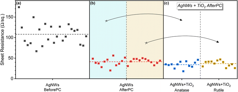
The electrical properties measured after each fabrication stage are compared in Fig. 2. There, individual statistics are presented for multiple groups of devices. Indeed, the average sheet resistance for the percolated silver nanowire network is Rsh = 108 Ω sq.−1 before treatment, and it is shown in Fig. 2(a). After the photonic sintering of the AgNWs, Fig. 2(b) shows an average Rsh = 41 Ω sq.−1 for the same 24 samples. This represents a 62% average reduction of the sheet resistance due to better contacts between the nanowires, as illustrated by the dashed gray and red lines. After the deposition of the photo-sensitive TiO2 precursor on all the samples, 12 samples are converted to anatase and 12 are converted to rutile. They are separated into the blue- and yellow-shaded areas in Fig. 2(b). The average sheet resistance of the 12 samples covered with anatase is Rsh = 34 Ω sq.−1, compared Rsh = 37 Ω sq.−1 for the samples covered with rutile TiO2. These averaged values represent an additional 6% reduction, compared with the standalone AgNWs electrodes. This additional reduction is attributed to the densification that occurs with the crystallization of TiO2.17 The presence of oxygen vacancies in the TiO2 precursor makes it sensitive to visible light, and crystallization is possible using photonic post-processing. These oxygen vacancies could contribute to enhance the conductivity in the films by facilitating charge transport, thanks to the vacancies acting as dopant states that shift the material's Fermi level close to the conduction band.50,51 Testing of this effect is out of the scope of this communication given its minor contribution to the TCE's final sheet resistance.
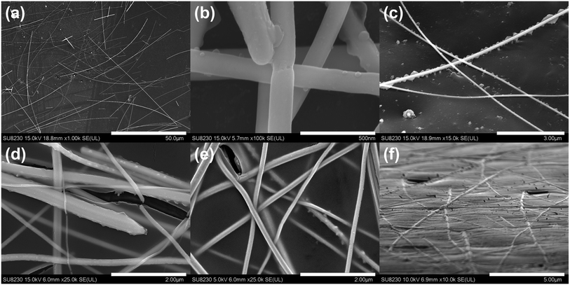
SEM images of the silver nanowire electrodes before, in Fig. 3(a), and after photonic sintering are shown in Fig. 3(b) and (c). These results suggest a good welding of the nanowire network as well as moderate penetration in the surface of the PET substrate after photonic treatment. In Fig. 3(c), we notice what appears to be a substrate's surface morphology change that comes as a result of the intense heat generated locally. This leads to partial melting of the substrate in the regions that are directly around and in close contact with the heated nanowires.21 This partial substrate melting did not globally change the optical properties and flexibility of the bulk film, but it has been reported that it can contribute to improving the adhesion to the substrate and the overall sturdiness of the film.5,8,21 The embedding of the nanowires and the local modification of the small regions of the PET substrate around the heated nanowire parts was resolved with the help of atomic force microscopy (AFM). These effects can be clearly appreciated in Fig. S1 of the ESI,† showing a sample of AgNWs AfterPC. In the areas without nanowires, the surface of the PET film remained unchanged, thus, the surface bumps are attributed to the excess heat generated at the nanowires during the photonic processing.
The silver nanowire electrodes covered with the TiO2 coating before photonic treatment are shown in Fig. 3(d) and (e). The same electrode after photonic treatment is shown in Fig. 3(f). This additional layer has been shown to provide thermal stability, environmental protection, sustainability, and protection against UV degradation for the nanowire film.17,45–47 It also provides the benefit of an additional functional layer of metal-oxide material that can be useful for device integration. Surface coverage with energy-dispersive X-ray spectroscopy (EDS) results are presented in Fig. S2 of the ESI section,† showing an approximately 400 nm TiO2 layer covering the nanowire film. The densification resulting from the crystallization of the amorphous TiO2 layer is known to potentially increase the close contact between the adjacent nanowires, leading to slight improvements in the overall sheet resistance of the film even after the initial flash-driven plasmonic welding.17 The versatility of the photonic sintering post-processing allows to dry and process films where residual solvents may be present, by using long-envelope pulses that facilitate the drying process and trigger the film's crystallization.11 This is shown in the secondary post-treatment step described in Fig. 1.
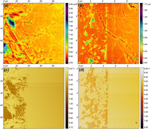
Atomic force microscopy (AFM) analysis was employed to investigate the surface topography of crystallized TiO2 films atop the AgNWs. Samples with AgNWs after photonic sintering (AgNWs AfterPC) were partially covered in transparent scotch tape. Then, the same TiO2 deposition and crystallization procedures took place. Finally, the tape was removed revealing an area with bare AgNWs next to an area completely covered by crystallized TiO2. The resulting AFM topography analysis shown in Fig. 4(a) and (b) presents the partial coverage of anatase and rutile TiO2, respectively. The scotch-tape tests also confirm the presence of AgNWs after its removal, showing the permanence of the nanowires embedded in the PET. Although precise film height estimation from AFM profiles proved challenging, a qualitative assessment was achieved by comparing image colors with the scale bar. The height of anatase film was estimated to be around 600 nm, shown in Fig. 4(a). The rutile-covered sample, Fig. 4(b), displayed an average height of around 400 nm. Inphase images in Fig. 4(c) and (d), facilitated the discrimination of coated and uncoated areas, demonstrating robust coverage of AgNWs by crystallized TiO2 films, as presented in Fig. 3. Importantly, the scotch-tape glue was affected by the photonic processing and transferred to the films upon removal. This is evidenced by regions whose height registered above the hybrid films, corresponding to green and above colors in the Fig. 4(a) and (b) and the darker regions in Fig. 4(c) and (d).
With respect to the optical properties of these hybrid TCEs, the deposition of the TiO2 layer impacts the overall transparency of the film by a small margin, with losses ranging between 1% and 2% when measured at 550 nm. In contrast, the amorphous TiO2 layer does increase the haze factor in the films, which is then changed by the photonic-induced crystallization post-processing. The comparisons for visible transmittance and haze can be observed in Fig. 5(a) and (b). The transmittance is measured for all samples presented in Fig. 2, while the haze was measured in one randomly selected sample after each fabrication step. The values presented in Table 1 correspond to the average transmittance and the haze values measured at 550 nm at each step of the fabrication process. Haze values are obtained using the technique described in the ESI in Fig. S4,† while the transmittance spectra for the 12 anatase and rutile samples are shown in Fig. S5.†
| Transmittance (%) | Haze (%) | |
|---|---|---|
| PET | 89.8 | 1.3 |
| PET + TiO2 | 88.4 | 1.3 |
| AgNWs BeforePC | 86.9 | 5.8 |
| AgNWs AfterPC | 86.5 | 8.9 |
| AgNWs + TiO2 AfterPC (anatase) | 85.0 | 7.8 |
| AgNWs + TiO2 AfterPC (rutile) | 85.2 | 7.7 |
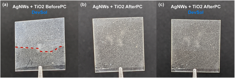
Two independent methods are used to confirm the crystallization of the TiO2 layer. First, we can use a modified developing solution (DevSol), whose preparation is described in the Methods section. This DevSol test is known to wash away the non-crystallized TiO2, while the crystalline TiO2 remains.2,31 This simple method helps to quickly determine the optimal pulse conditions to yield a crystalline structure, as a 15 second immersion and subsequent washing in DI water are enough to establish the crystallinity state of our films. Fig. 6(a) shows a sample with an amorphous TiO2 layer (AgNWs + TiO2 BeforePC) that failed the DevSol test. Because of the transparency of the TiO2 film, the red dashed line in Fig. 6(a) helps to distinguish between the washed-away top region from the unwashed bottom. For contrast, a sample where the layer is fully crystallized (AgNWs + TiO2 AfterPC) is shown in Fig. 6(b) and, that same sample after it was immersed in the DevSol for 15 seconds in Fig. 6(c) maintaining its integrity and the coverage of the TiO2 layer.
In turn, Raman spectroscopy can be used to assess the samples that passed the DevSol test. Raman micro-spectroscopy results from Fig. 5(c) clearly show the anatase and rutile TiO2 signatures after the proper photonic treatment. As such, these results confirm that this precursor can be controllably-converted to anatase or rutile TiO2 depending on the target application. Most importantly, this can be done with little consequences on both the Rsh values and the optical transmittance of this hybrid TCE architecture as shown in Fig. 2 and 5(a). It is very hard to obtain conclusive XRD measurements from smooth thin films of TiO2 atop a PET substrate and AgNWs in between. The PET substrate generates a strong signal that completely obscures any other signal coming from the hybrid-TCE constituents. Dried TiO2 precursor, compressed in pellet form enables proper XRD characterization of the crystalline state after the photonic processing has taken place. Fig. S3(a) and (b)† show the crystallization of these pellets processed to yield anatase and rutile phases.
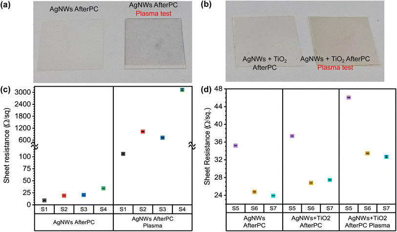
Finally, it was previously shown that conformal coatings using TiO2 to cover silver nanowire films offer environmental protection against degradation and oxidation of the silver, thus preserving its electrical properties.17,44–46 We chose to test the additional protection offered by the crystallized TiO2 coating by exposing a new set of samples to oxygen plasma during a brief period. Experimental results shown in Fig. 7 clearly indicate that only 40 seconds of plasma exposure at 50 W ionization power is enough to increase the sheet resistance of the unprotected electrodes by several orders of magnitude. Higher ionization power or longer exposure times easily break the unprotected films, and it becomes impossible to measure the sheet resistance value throughout the whole film. Fig. 7(a) shows that unprotected samples turned dark as a result of the forced oxidation of the silver,52 unlike the samples protected by a thin crystallized TiO2 coating and shown in Fig. 7(b). Fig. 7(c) and (d) compare the sheet resistance values for the hybrid TCEs before and after the oxygen plasma treatment. In Fig. 7(c), bare silver nanowire films (samples S1–S4) show a pronounced increase in their Rsh compared to the samples S5–S7 that were protected by the thin crystallized TiO2 coating. These changes in Rsh are highlighted in Fig. 7(d).
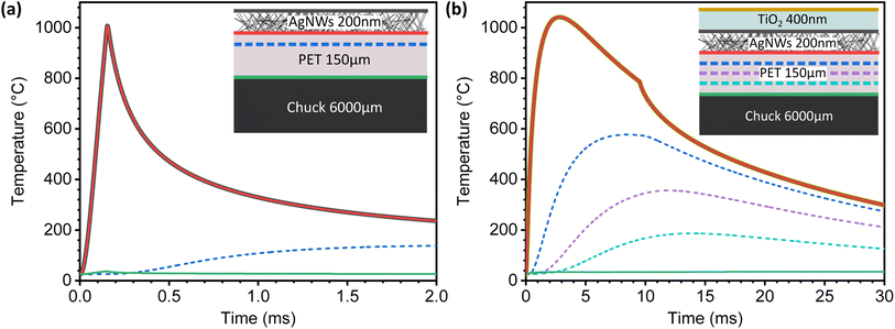
A useful tool to visualize the heat dissipation during both rounds of photonic sintering is through the SimPulse simulation tool available within the PulseForge Invent system. This simulation can allow us to better understand the macroscopic effects of the photonic post-processing parameters on the substrate to avoid thermally-induced structural damage. There, layers of material can be stacked atop each other, and the simulation shows the temperature time profile at each interface and at specific chosen depths. In Fig. 8(a), simulations suggest that direct heating of the silver nanowires occurs during the first 150 μs of the first pulse. Then, rapid cooling dominates thanks to the thermal mass present in the substrate. As expected, the whole nanowire film and the surface of the PET follow the same temperature profile. Moving deeper into the substrate after 25% of the total thickness, the temperature profile stays below 200 °C as represented by the dashed blue line. The continuous green line illustrates how the bottom of the PET barely registers any temperature increase throughout the entire process due to the significant thermal gradient.
In contrast, the transient temperature profile of the device with the TiO2 coating shows a synergistic effect. We assume that both the silver nanowires and amorphous TiO2 follow the same temperature progression as their simulated profiles are perfectly superimposed in Fig. 8(b) as shown by the yellow, dark grey and red continuous lines. Of course, this heating profile is most likely to be non-uniform, with a local heating effect more pronounced around the nanowires. Even though the system reaches temperatures of over 1000 °C, the nanowire network easily transfers this excess heat to both the substrate and the TiO2 coating, helping with the crystallization process.53 In this case, we analyze the temperature profile inside the PET substrate at 25, 50 and 75% of the PET's total thickness, shown in Fig. 8(b). At around 75% of the substrate's thickness, the temperature never surpasses 200 °C, which is in line with the thermal specifications of the PET substrate, thus avoiding damage to it.
3 Discussion
Conceptually, it is somewhat surprising to observe that the silver nanowire film's properties remain mostly unchanged when a long pulse is used to crystallize the thin amorphous TiO2 coating. Pulses of 10's to 100's of microseconds in duration quickly raise the temperature of the metallic nanowires, enabling the formation of strong joints at the points where the nanowires are in contact. This occurs thanks to the almost instantaneous localized heat generation along the nanowire network as a result of the surface plasmon resonance that metallic nanostructures exhibit in the visible portion of the electromagnetic spectrum.23,42 Because plasmon-induced welding is self-limiting, the heat accumulation at the intersections stops once the joining process occurs.9 When the absorbed photonic energy converts into heat, it then spreads throughout the whole percolated nanowire network before being dissipated in the substrate. This suggests that heat dissipation from the AgNWs is facilitated by the superior heat capacity and low thermal conductivity of the substrate.4 Additionally, direct contact with the aluminum chuck cools the substrate's back, creating a large thermal gradient. Finally, increasing the pulse fluence by adjusting the time envelope can facilitate greater heat transfer from the nanowires to the substrate.4 For the case of the longer pulses used to crystallize the TiO2 layer, the heating is much slower. This favors the ceramic crystallization process while still giving sufficient time for the surface of the substrate to reach thermal equilibrium, preventing any thermally-induced damage, even though the temperature reached at the substrate's surface is much higher, as seen in Fig. 8(b).This can be understood from the thermal equilibration time τ calculated for each of the materials involved.7 Based on the material parameters available in the SimPulse simulation, a 150 μm-thick PET substrate possesses a τPET = 23 ms, for a 200 nm-thick film of silver nanowires is τAgNWs = 58 ps approximately54 and the TiO2 coating possesses a τTiO2 = 7 ns approximately, a value that is obtained from the database present in the SimPulse software. One of the conditions necessary to achieve successful photonic curing of materials is that the pulse duration (tp) must be much shorter than the thermal equilibrium time of the substrate (τPET = 23 ms, from SimPulse material database). In this case, the heat generation coming from the silver nanowire film can be dissipated into the substrate. If the nanowires are processed using a longer pulse envelope comparable to τPET, the absorbed energy will transfer to the substrate too fast to properly weld the film of nanowires. This also explains why the pulse conditions used to crystallize the TiO2 layer does not affect the Rsh of the already treated nanowire film, even if the pulse fluence is about 6× times higher than the pulses used to process the nanowires. Indeed, higher fluence in longer pulses does not necessarily translate into higher peak power density (PPD). The short pulse used in the photonic treatment of the silver nanowires possesses a PPD of 7.21 kW cm−2, whereas the long pulse with higher fluence used in the crystallization of the TiO2 only delivers a PPD of 0.69 kW cm−2 using a Gaussian pulse profile.
Although the τTiO2 is almost 1000× greater than that of the AgNWs, it remains shorter than the pulse's duration, meaning that the crystallization process should not damage the substrate, as shown in Fig. 8(b). However, photonic crystallization of the TiO2 layer atop the silver nanowire layer requires a more advanced analysis. The presence of oxygen vacancies in the TiO2 precursor modifies its optical absorption levels, extending them to longer wavelengths.55,56 As such, photons with less energy than the nominal TiO2 bandgap can still be absorbed and trigger the crystallization.36–38 The presence of the silver nanowires also helps inducing the crystallization of the TiO2 coating by converting their absorbed photonic energy as heat, because silver is a much better absorber than TiO2.53,57 Additionally, the presence of the metallic atoms promotes the reorganization of the Ti–O bonds into lower energetic states, which improves the crystallization.57,58 Indeed, we tested the TiO2 film crystallization atop the PET substrate without the AgNWs using the same photonic post-processing conditions reported for both anatase and rutile phases. These results shown in the ESI Fig. S6† demonstrate that we cannot obtain a crystalline layer. As a result, these samples all failed the DevSol immersion test. These results confirm the contribution of the silver nanowires to the metal-induced crystallization of the TiO2.
4 Conclusions
We report a facile fabrication route to produce hybrid transparent conductive electrodes (TCEs) on flexible PET. Their optical and electronic properties are comparable with previously-reported single-material silver nanowire-based TCEs. Our best devices consist of a layer of AgNWs covered with anatase TiO2. They boast an average optical transparency of 84% and haze value of 7.7% at 550 nm, with a sheet resistance down to 18 Ω sq.−1. These results are obtained through the carefully-controlled photonic treatment of each layer separately. Indeed, a single 1 × 1 inch hybrid TCE sample can be entirely fabricated in less than an hour, including the cleaning and preparation of the PET substrate and the post-processing of each of the layers.The successful welding of silver nanowires on flexible polymeric substrates and the optically-induced crystallization of TiO2 layers for applications in optoelectronic devices have been previously demonstrated independently. However, integrating both materials and post-processing together is a new development in the field of additive manufacturing for flexible electronics. We demonstrate that this understanding the synergistic post-processing effects of each material allows to treat simultaneously a wide array of materials using industry-grade photonic sintering machine.
We use a known developing solution test as a fast and reliable approach to test the crystallization of thin-film metal-oxides, a method that can be efficiently incorporated in production lines for effective quality control at any point of the fabrication processes. It also tests the compatibility of our TCE's with fabrication processes for devices where contact with solvents and other chemicals could potentially damage either the AgNWs or TiO2. Also, oxygen plasma is used for quality control and to test the accelerated degradation of our TCEs.
To the best of our knowledge, this is the first hybrid-material transparent conductive electrode architecture that is completely treated by photonic sintering methods. Taking advantage of the diverse processing demands of different materials, it is possible to envision higher number layers of different materials that can be assembled this way, to create functional devices with very short processing times. As such, we firmly believe that this work helps bring flexible hybrid TCEs closer to large-scale manufacturing capabilities.
5 Experimental section
5.1 Material preparation
Silver nanowires with average diameter of 100 nm and length from 100 to 200 μm dispersed in ethanol with a concentration of 20 mg mL−1 were purchased and used as-received from ACS Materials (Agnw-L100). The substrate is heat stabilized polyester film purchased from Tekra (Melinex ST505). Titanium(IV) butoxide (TNBT), ethanol anhydrous, acetylacetone (acac) and acetic acid anhydrous >99% were procured from Millipore Sigma and used as-purchased. To prepare the defect rich, light sensitive, amorphous TiO2 precursor, 28.853 g of ethanol mixed with 1.474 g of acac were placed under magnetic stirring for 20 minutes. Then, 1.860 g of TNBT were added, while maintaining the stirring for additional 40 minutes. Hydrolysis was triggered by adding dropwise 0.84 mL of DI water. This solution is covered in parafilm to restrict contact with air and contaminants and then, is left aging for 8 months. The resulting solution was diluted in anhydrous ethanol at 10% w/w concentration ready for deposition.5.2 Assembly of the silver nanowire networks and deposition of titanium dioxide layer
The PET substrates were cleaned with IPA alcohol and prepared for oxygen plasma cleaning for 10 minutes at 150 Watts using a PE-100 system from PlasmaEtch. After, the PET substrates were cut in 22 × 22 mm squares and placed on the spin coater chuck. The deposition of the AgNW film was done applying 300 μL of Agnw-L100 solution on the still substrate, ensuring complete area coverage. The spin coating process is then started at 4000 rpm for 45 s. Afterwards, the first round of photonic sintering processing took place using a PulseForge Invent system from Novacentrix. Subsequently, 200 μL of the amorphous TiO2 precursor was drop-casted completely covering the sample and a second spin coating process took place at 4000 rpm for 45 s. After, the second round of photonic sintering processing took place to crystallize the TiO2 layer.5.3 Developing solution (DevSol) preparation and testing
The solution was prepared by adding 2 mL of acetic acid in 20 mL of 1![[thin space (1/6-em)]](https://www.rsc.org/images/entities/char_2009.gif) :
:![[thin space (1/6-em)]](https://www.rsc.org/images/entities/char_2009.gif) 3 DI water to methanol mix. To help identify the effects of the DevSol test, the samples were partially immersed, leaving half of the sample untouched. The immersion took place for 15 seconds and after, de-ionized water was used to wash the samples.
3 DI water to methanol mix. To help identify the effects of the DevSol test, the samples were partially immersed, leaving half of the sample untouched. The immersion took place for 15 seconds and after, de-ionized water was used to wash the samples.
5.4 Sample characterization
Sheet resistance was measured using the 4-point probe system from Ossila. Optimization of the best photonic curing conditions to weld the AgNW film was done by only measuring the samples before and after in the same center spots, previously marked for uniformity of the measures. Rapid proof of crystallization of the TiO2 precursor was done following a modified version of rinse-in developing procedure reported elsewhere.2,31 Plasma ageing was done using the same PE-100 PlasmaEtch system, set to 50 Watts for 40 seconds. Raman characterization is done using a WITec Alpha300 confocal Raman microscope equipped with a 60 mW fiber-coupled CW laser at 532 nm emission wavelength and a mechanical attenuator. SEM and EDS imaging was done using a SU8230 from Itachi. XRD was done using a Bruker D8 Advance, equipped with a Cu source. Atomic force microscopy analysis was done using a Bruker MultiMode8-HR AFM. Optical transmittance and haze analysis were done using a UV-VIS-NIR spectrophotometer PerkinElmer, Lambda 750 with an integrating sphere. Haze measures were performed following the procedure described in the ESI.†Author contributions
The concept and methodology were planned and done by L. F. G. and S. G. C.; fabrication of the samples and testing done by L. F. G.; synthesis of the TiO2 precursor done by J. A. B.; characterization done by L. F. G. and J. A. B. and analysis of the results was done by L. F. G., J. A. B., S. G. C.; the first version of manuscript was written by L. F. G. and S. G. C. The manuscript was reviewed and commented by L. F. G., J. A. B., S. G. C.Conflicts of interest
The authors declare no conflict of interests for the publication of this manuscript.Acknowledgements
S. G. C. thanks the Canada Research Chair and the NSERC Discovery programs for their support.Notes and references
- S. Das, G. Gu, P. C. Joshi, B. Yang, T. Aytug, C. M. Rouleau, D. B. Geohegan and K. Xiao, J. Mater. Chem. A, 2016, 4, 9685–9690 RSC.
- T. B. Daunis, K. A. Schroder and J. W. P. Hsu, npj Flexible Electron., 2020, 4, 1–7 CrossRef.
- B. Feleki, G. Bex, R. Andriessen, Y. Galagan and F. Di Giacomo, Mater. Today Commun., 2017, 13, 232–240 CrossRef CAS.
- Y.-R. Jang, S.-J. Joo, J.-H. Chu, H.-J. Uhm, J.-W. Park, C.-H. Ryu, M.-H. Yu and H.-S. Kim, Int. J. Precis. Eng. Manuf.–Green Technol., 2020, 8, 327–363 CrossRef.
- J. Jiu, M. Nogi, T. Sugahara, T. Tokuno, T. Araki, N. Komoda, K. Suganuma, H. Uchida and K. Shinozaki, J. Mater. Chem., 2012, 22, 23561–23567 RSC.
- R. T. Piper, T. B. Daunis, W. Xu, K. A. Schroder and J. W. P. Hsu, Front. Energy Res., 2021, 9, 12 Search PubMed.
- K. Schroder, TechConnect Briefs, 2011, vol. 2, pp. 220–223 Search PubMed.
- C.-H. Song, K.-H. Ok, C.-J. Lee, Y. Kim, M.-G. Kwak, C. J. Han, N. Kim, B.-K. Ju and J.-W. Kim, Org. Electron., 2015, 17, 208–215 CrossRef CAS.
- S. Bansal and R. Malhotra, Nanotechnology, 2016, 27, 495602 CrossRef CAS PubMed.
- M. Dexter, R. Bhandari, C.-H. Chang and R. Malhotra, RSC Adv., 2017, 7, 56395–56405 RSC.
- Y. Noh, G. Y. Kim, H. Lee, J. Shin, K. An, M. Kumar and D. Lee, Nanotechnology, 2022, 33, 272001 CrossRef PubMed.
- F. Zamanpour, F. Behrouznejad, E. Ghavaminia, R. Khosroshahi, Y. Zhan and N. Taghavinia, ACS Appl. Energy Mater., 2021, 4, 7800–7810 CrossRef CAS.
- L. F. Gerlein, J. A. Benavides-Guerrero and S. G. Cloutier, Sci. Rep., 2021, 11, 24156 CrossRef CAS PubMed.
- S. B. Sepulveda-Mora and S. G. Cloutier, J. Nanomater., 2012, 2012, 7 Search PubMed.
- Y. Sun, B. Gates, B. Mayers and Y. Xia, Nano Lett., 2002, 2, 165–168 CrossRef CAS.
- Y. Sun, Y. Yin, B. T. Mayers, T. Herricks and Y. Xia, Chem. Mater., 2002, 14, 4736–4745 CrossRef CAS.
- T.-B. Song, Y. S. Rim, F. Liu, B. Bob, S. Ye, Y.-T. Hsieh and Y. Yang, ACS Appl. Mater. Interfaces, 2015, 7, 24601–24607 CrossRef CAS PubMed.
- D. Azulai, T. Belenkova, H. Gilon, Z. Barkay and G. Markovich, Nano Lett., 2009, 9, 4246–4249 CrossRef CAS PubMed.
- M. M. Menamparambath, K. Yang, H. H. Kim, O. S. Bae, M. S. Jeong, J.-Y. Choi and S. Baik, Nanotechnology, 2016, 27, 465706 CrossRef PubMed.
- C. Preston, Y. Xu, X. Han, J. N. Munday and L. Hu, Nano Res., 2013, 6, 461–468 CrossRef CAS.
- J. H. Park, G.-T. Hwang, S. Kim, J. Seo, H.-J. Park, K. Yu, T.-S. Kim and K. J. Lee, Adv. Mater., 2017, 29, 1603473 CrossRef PubMed.
- J. Niittynen, E. Sowade, H. Kang, R. R. Baumann and M. Mäntysalo, Sci. Rep., 2015, 5, 8832 CrossRef CAS PubMed.
- E. C. Garnett, W. Cai, J. J. Cha, F. Mahmood, S. T. Connor, M. Greyson Christoforo, Y. Cui, M. D. McGehee and M. L. Brongersma, Nat. Mater., 2012, 11, 241–249 CrossRef CAS PubMed.
- G. H. Chan, J. Zhao, E. M. Hicks, G. C. Schatz and R. P. Van Duyne, Nano Lett., 2007, 7, 1947–1952 CrossRef CAS.
- D.-H. Lee, Y.-J. Chang, G. S. Herman and C.-H. Chang, Adv. Mater., 2007, 19, 843–847 CrossRef CAS.
- W. Scheideler and V. Subramanian, Nanotechnology, 2019, 30, 272001 CrossRef CAS PubMed.
- A. M. Weidling, V. S. Turkani, B. Luo, K. A. Schroder and S. L. Swisher, ACS Omega, 2021, 6, 17323–17334 CrossRef CAS PubMed.
- J. Bai and B. Zhou, Chem. Rev., 2014, 114, 10131–10176 CrossRef CAS PubMed.
- Y. Bai, I. Mora-Seró, F. De Angelis, J. Bisquert and P. Wang, Chem. Rev., 2014, 114, 10095–10130 CrossRef CAS PubMed.
- S.-P. Chen, J. R. D. Retamal, D.-H. Lien, J.-H. He and Y.-C. Liao, RSC Adv., 2015, 5, 70707–70712 RSC.
- T. B. Daunis, D. Barrera, G. Gutierrez-Heredia, O. Rodriguez-Lopez, J. Wang, W. E. Voit and J. W. P. Hsu, J. Mater. Res., 2018, 33, 2454–2462 CrossRef CAS.
- F. Di Giacomo, V. Zardetto, A. D'Epifanio, S. Pescetelli, F. Matteocci, S. Razza, A. Di Carlo, S. Licoccia, W. M. M. Kessels, M. Creatore and T. M. Brown, Adv. Energy Mater., 2015, 5, 1401808 CrossRef.
- J. Hwang, K. Lee, Y. Jeong, Y. U. Lee, C. Pearson, M. C. Petty and H. Kim, Adv. Mater. Interfaces, 2014, 1, 1400206 CrossRef.
- I. Jeong, H. Jung, M. Park, J. S. Park, H. J. Son, J. Joo, J. Lee and M. J. Ko, Nano Energy, 2016, 28, 380–389 CrossRef CAS.
- T. Nakajima, K. Shinoda and T. Tsuchiya, Chem. Soc. Rev., 2014, 43, 2027–2041 RSC.
- J. A. Benavides, C. P. Trudeau, L. F. Gerlein and S. G. Cloutier, ACS Appl. Energy Mater., 2018, 1, 3607–3613 CrossRef CAS.
- J. A. Benavides-Guerrero, L. F. Gerlein, C. Trudeau, D. Banerjee, X. Guo and S. G. Cloutier, Sci. Rep., 2022, 12, 15441 CrossRef CAS PubMed.
- L. F. Gerlein, J. A. Benavides-Guerrero and S. G. Cloutier, Adv. Eng. Mater., 2019, 22, 1901014 CrossRef.
- B. Qian and Z. Shen, J. Asian Ceram. Soc., 2013, 1, 315–321 CrossRef.
- A. Zocca, P. Colombo, C. M. Gomes and J. Günster, J. Am. Ceram. Soc., 2015, 98, 1983–2001 CrossRef CAS.
- H.-J. Hwang and H.-S. Kim, J. Nanosci. Nanotechnol., 2015, 15, 5028–5034 CrossRef CAS PubMed.
- S. Luo, S. Zhang, B. B. Bourgeois, B. C. Riggs, K. A. Schroder, Y. Zhang, J. He, S. Adireddy, K. Sun, J. T. Shipman, M. M. Oguntoye, V. Puli, W. Liu, R. Tu, L. Zhang, S. Farnsworth and D. B. Chrisey, J. Mater. Res., 2017, 32, 1701–1709 CrossRef CAS.
- C.-H. Chung, T.-B. Song, B. Bob, R. Zhu and Y. Yang, Nano Res., 2012, 5, 805–814 CrossRef CAS.
- J.-J. Huang, T.-F. Cheng, Y.-R. Ho and D.-P. Huang, Thin Solid Films, 2021, 736, 138903 CrossRef CAS.
- D. G. Lee, D. Lee, J. S. Yoo, S. Lee and H. S. Jung, Nano Convergence, 2016, 3, 20 CrossRef PubMed.
- M.-H. Yeh, P.-H. Chen, Y.-C. Yang, G.-H. Chen and H.-S. Chen, ACS Appl. Mater. Interfaces, 2017, 9, 10788–10797 CrossRef CAS PubMed.
- P. Ramasamy, D.-M. Seo, S.-H. Kim and J. Kim, J. Mater. Chem., 2012, 22, 11651–11657 RSC.
- J. Resende, A. Sekkat, V. H. Nguyen, T. Chatin, C. Jiménez, M. Burriel, D. Bellet and D. Muñoz-Rojas, Small, 2021, 17, 2007344 CrossRef CAS PubMed.
- T. Rajaraman, S. P. Parikh and V. G. Gandhi, Chem. Eng. J., 2020, 389, 123918 CrossRef CAS.
- D. Maarisetty and S. Sundar Baral, J. Mater. Chem. A, 2020, 8, 18560–18604 RSC.
- H. H. Pham and L.-W. Wang, Phys. Chem. Chem. Phys., 2014, 17, 541–550 RSC.
- L. O. Akinsinde, T. E. Glier, M. Schwartzkopf, M. Betker, M. Nissen, M. Witte, S. Scheitz, C. Nweze, B. Grimm-Lebsanft, M. Gensch, A. Chumakov, I. Baev, U. Schürmann, T. Dankwort, F. Fischer, M. Martins, S. V. Roth, L. Kienle and M. Rübhausen, Appl. Surf. Sci., 2021, 550, 149362 CrossRef CAS.
- L. Lermusiaux, A. Mazel, A. Carretero-Genevrier, C. Sanchez and G. L. Drisko, Acc. Chem. Res., 2022, 55, 171–185 CrossRef CAS PubMed.
- S. Ji, W. He, K. Wang, Y. Ran and C. Ye, Small, 2014, 10, 4951–4960 CrossRef CAS PubMed.
- X. Pan, M.-Q. Yang, X. Fu, N. Zhang and Y.-J. Xu, Nanoscale, 2013, 5, 3601–3614 RSC.
- A. Sarkar and G. G. Khan, Nanoscale, 2019, 11, 3414–3444 RSC.
- C. Yang, Y. Hirose, S. Nakao, N. L. H. Hoang and T. Hasegawa, Appl. Phys. Lett., 2012, 101, 052101 CrossRef.
- D. Wong, O. Abuzalat, S. Mostafa, S. Kim and S. S. Park, IEEE Sens. J., 2019, 19, 9113–9121 CAS.
Footnote |
| † Electronic supplementary information (ESI) available. See DOI: https://doi.org/10.1039/d3ra07103k |
| This journal is © The Royal Society of Chemistry 2024 |

