
 Open Access Article
 This Open Access Article is licensed under a Creative Commons Attribution-Non Commercial 3.0 Unported Licence
Investigation of the electronic and optical properties of bilayer CdS as a gas sensor: first-principles calculations
Warood Kream
Alaarage
a,
Abbas H.
Abo Nasria
 *b,
Tamadhur Alaa
Hussein
b and
Hamid Ibrahim
Abbood
c
*b,
Tamadhur Alaa
Hussein
b and
Hamid Ibrahim
Abbood
c
aFaculty of Dentistry, University of Kufa, Najaf, Iraq. E-mail: Wuroodk.olaiwi@uokufa.edu.iq
bDepartment of Physics, Faculty of Science, University of Kufa, Najaf, Iraq. E-mail: abbas.abonasiriya@uokufa.edu.iq
cAl-Zahraa University for Women, Iraq. E-mail: hamid.ibrahim@alzahraa.edu.iq
First published on 15th February 2024
Abstract
We utilised first-principles computations based on density functional theory to investigate the optical and electronic properties of bilayer CdS before and after the adsorption of gas molecules. Initially, we examined four candidate adsorption sites to determine the best site for adsorbing CO, CO2, SO2, H2S, and SO. In order to achieve the optimal adsorption configurations, we analysed the adsorption energy, distance, and total charge. Our findings reveal that the CdS bilayer forms a unique connection between the O and Cd atoms, as well as the S and Cd atoms, which renders it sensitive to SO2, H2S, and SO through chemical adsorption, and CO and CO2 through strong physical adsorption. The adsorption of gas molecules enhances the optical properties of the CdS bilayer. Consequently, the CdS bilayer proves to be a highly efficient gas sensor for SO2, H2S, and SO gases.
1. Introduction
Sensing toxic gas molecules is crucial for various applications, including space missions, medical and agricultural fields, environmental pollution monitoring, chemical process control, and more.1,2 Gases such as CO, CO2, SO2, H2S, and SO are generated from burning chemical fuels, coal, plastics, and car exhaust. These gases can hinder the absorption of oxygen by tissues, although their levels of danger may vary.3–6 Therefore, there has been significant attention given to the development and discovery of novel, highly sensitive materials for gas sensing. Since Novoselov et al.'s groundbreaking work on 2D nanomaterials in 2004, there has been a significant emphasis on exploring the potential of this material class for cutting-edge gas sensor applications.7 The mechanical cracking method has been widely employed for the separation of graphene from graphite, owing to its intriguing optical, physical, mechanical, magnetic, and electrical properties.8–10 These unique properties endow graphene with tremendous potential for significant advancements in material science and innovation. The remarkable properties of graphene and its derivatives open up promising avenues in various fields, including optoelectronic devices, catalysts, photocatalysis, transistors, nanoelectromechanical devices, nanoscale devices, gas sensors, and photodetectors.11–20 In addition, the research on the gas response in 2D nanomaterials like C3N,21 InN,22 GaN,23 TI2O,24 AlN,25–27 SiGe,28 BN,29–31 GaS, GaSe,32 silicene,33 SnSe,34 BNNTs,35 InP,36 and borospherene37,38 has been developed in recent decades.Recent research has shown that CdS-based composites, such as CdS-supramolecular organogel hybrid films39 and CdS–SnO2 composites,40 exhibit high sensitivity to volatile organic compounds. Moreover, sensors have been developed based on n-CdS/p-polyaniline thin film heterojunctions41 and leaf-like CdS micro-/nanostructures.42 They have displayed improved performance, such as response, recovery time, stability, and recognition ability towards various analytes. Several methods have been employed to prepare nanocrystalline CdS thin films, including physical and chemical techniques such as sol–gel,43 gas evaporation,44 and electrostatic deposition,45 among others. Researchers have investigated the interaction of oxygen gas with CdS films prepared through spray pyrolysis46 and reported on the resistive type humidity sensing properties of CdS nanoparticles grown through the chemical bath deposition (CBD) method.47 CdS supramolecular organogel hybrid films have been fabricated through the exposure of a supramolecular organogel film containing Cd(Ac)2 to an H2S atmosphere at room temperature,39 and n-CdS/p-polyaniline thin film heterojunction-based liquefied petroleum gas (LPG) sensors have been produced utilising a simple and cost-effective electrodeposition technique.41 CBD is a favoured option among film deposition methods due to its suitability for large-scale fabrication processes, simplicity, cost-effectiveness, and non-polluting properties. CBD produces homogeneous, hard, adhesive, transparent, and stoichiometric nanocrystalline thin films.48 The availability of cost-effective and simple practical methods for synthesising CdS slabs has motivated the industry and research communities' efforts to look on employing CdS for sensing applications.43,48,49
Recently, cadmium sulfide (CdS) has gained recognition as an exceptional material for optoelectronic devices, primarily due to its position as a significant II–VI compound semiconductor with a direct band gap of 2.42 eV.50–56 Multiple methods for synthesizing CdS have been extensively explored, encompassing chemical bath deposition, thermal evaporation, ultrasonic spray pyrolysis, and atomic layer epitaxy.57–59 CdS is commonly recognized for its application as a pigment; however, its utility extends to various other contexts, including piezoelectric transducers, solar cells, photoresistors, photovoltaics, and transistors. The advantageous characteristics of CdS, such as photoconductivity, electroluminescence, and piezoelectricity, enable these applications to operate effectively in high-frequency ranges.60–66 CdS exhibits chemoresistiveity in addition to its more common uses, yet this intriguing quality has received relatively little attention from researchers. The utilization of CdS as a gas sensor has been documented in only a limited number of publications.
Moreover, it has been observed that light at room temperature can activate the chemoresistiveity in CdS. By energizing electrons into the conduction band, electromagnetic irradiation can modify the surface chemistry of the film and enhance its conductivity. This unique property allows CdS gas sensors to operate effectively at room temperature, eliminating the need for external heating.67,68 Consequently, there is a need to explore CdS as a novel material in the gas sensor field. Therefore, 2D CdS bilayers emerge as excellent candidates for highly sensitive gas sensors, given their potential for exceptional gas-sensing capabilities.
The enhancement of the surface performance for several adsorption systems has previously been confirmed through employing double-layers of the slab.69–71 Here, we have employed a two layers of CdS to replicate the surface behaviour and properties to reproduce the experimental measured structures of the system which would be typical of a semi-infinite CdS slab. The efficacy of replicating a CdS surface behavior and properties using two layers was investigated in the study72 by Qasrawi and Abed. The use of a pre-assembled CdS seed layer prior to CdSe deposition has been reported to improve the performance of quantum dot-sensitized solar cells.73
In this study, we aimed to explore the potential of CdS bilayers as gas sensors for CO, CO2, SO2, H2S, and SO gases. To achieve this, we conducted first-principle calculations using density functional theory (DFT) to analyze the adsorption behavior of these gases on the CdS bilayer. Additionally, we systematically investigated the adsorption of CO, CO2, SO2, H2S, and SO gas molecules on CdS bilayers to facilitate a comprehensive and comparative discussion. Our investigation encompassed the adsorption of gas molecules as well as the electronic and optical properties of the bilayer CdS. Based on our findings, CdS bilayers exhibit promising potential as gas sensors, particularly for H2S and SO. It is crucial to acknowledge that the findings of this research are based on no experimental evidence. Therefore, it is imperative for us to produce strong and conclusive results in order to drive additional experimental investigation in the future.
2. Computational details
The DFT was the basis for all calculations in this paper,74 with the generalised gradient approximation75–77 and the Perdew–Burke–Ernzerhof function used to describe the exchange–correlation interaction.78–80 The dispersion-corrected DFT approach and Grimme correction were applied to the computations to appropriately represent van der Waals interactions,9,46,47 and the DNP base set was tuned to 4.4. Dmol3 code was used for structural optimisation and electronic property calculations, with the k-points set to 10 × 10 × 1 and 15 × 15 × 1, respectively.81,82 The optical properties were calculated using the CASTEP code,83,84 with the k-points set to 7 × 7 × 1, the energy cutoff set to 350 eV, and the smearing value set to 0.005 Ha (1 Ha = 27.2114 eV).85 The Heyd–Scuseria–Ernzerhof hybrid functional HSE06 (ref. 86) is also used to improve the determination of the considered 2D materials' electronic properties, as theoretical experience has shown that the standard functionals always tend to underestimate the band gap of materials. A vacuum space thickness of around 20 Å was used to prevent interactions between layers. G (0, 0, 0)–F (0, 0.5, 0)–M (0.333, 0.667, 0) was employed as the Brillouin zone path for energy band analysis.In line with other studies, the system is composed of a CdS bilayer with a 3 × 3 supercell (36 atoms) and a lattice constant of a = b = 12.619![[thin space (1/6-em)]](https://www.rsc.org/images/entities/char_2009.gif) 605 and c = 25.067658.87 To evaluate a gas molecule's adsorption system on a CdS bilayer is stable, the adsorption energy defined (Ead) as follows:88
605 and c = 25.067658.87 To evaluate a gas molecule's adsorption system on a CdS bilayer is stable, the adsorption energy defined (Ead) as follows:88
| Ead = ECdS + gas − ECdS − Egas, | (1) |
To assess the interaction between gases and the CdS bilayer, we have calculated the interaction energies using the following expression:
| Eint = ECdS+gas − [ECdS + Egas] − δBSSE, | (2) |
3. Results and discussion
3.1 Pristine CdS bilayer's structural properties
The phonon dispersion curves of the pristine CdS bilayer were calculated at the equilibrium state to verify its stability, as depicted in Fig. 1. The phonon dispersion curves of the pristine CdS bilayer exhibit no indications of soft phonon modes, thereby demonstrating the dynamic stability of the bilayer at the equilibrium state.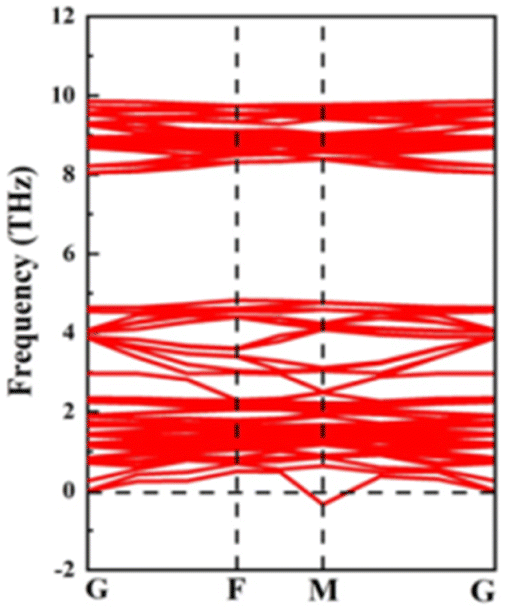 | ||
| Fig. 1 Phonon dispersion curves of pristine CdS bilayer. | ||
Fig. 2 illustrates the optimized structures of the supercell of the pristine CdS bilayer from both top and side views, as well as the energy band structure of the bilayer CdS. The top view highlights the resemblance between graphene and the double-layer CdS, both exhibiting hexagonal structures. The Cd–S bond length measures 2.571 Å. To explore the gas adsorption behavior in different orientations (parallel or perpendicular to the bilayer), four adsorption sites, namely T1 (Cd), T2 (S), T3 (center), and T4 (bridge), were utilized on the supercell of the bilayer CdS (as shown in Fig. 2). The initial adsorption distance in various adsorption sites was set at approximately 3 Å. The adsorption energy (Ead) serves as an indicator of bilayer stability, with lower values indicating more stable structures. The most stable energetic sites for CO, CO2, SO2, H2S, and SO on the CdS bilayer are the S, Cd, S, Cd, and S sites, respectively, as presented in Table 1.85 For the CdS bilayer, the spacing between the layers (h = 4.2 Å) is greater than the sum of any two atoms' radii in the bilayer (the atomic radii of Cd and S are rCd = 1.51 Å and rS = 1.02 Å).92 The energy band structure of bilayer CdS is shown in Fig. 2. At the G point, the valence band maximum (VBM) and the conduction band minimum (CBM) are both in bilayer CdS, which has a direct band gap (Eg) of 1.499 eV.
 | ||
| Fig. 2 Top, side views and band structure of the optimised CdS bilayer structures. | ||
| Adsorption systems | Site | E ad (eV) | d (Å) | r (Å) | Q (|e|) | Style |
|---|---|---|---|---|---|---|
| CO/CdS-bilayer | Cd | −0.40 | 3.07 | 2.28 (C–Cd) | 0.01 | Donor |
| S | −0.48 | 2.85 | 2.28 (C–Cd) | 0.02 | Donor | |
| Bridge | −0.42 | 3.21 | 2.28 (C–Cd) | 0.01 | Donor | |
| Center | −0.42 | 3.22 | 2.28 (C–Cd) | 0.02 | Donor | |
| CO2/CdS-bilayer | Cd | −0.44 | 3.04 | 2.24 (O–Cd) | −0.02 | Acceptor |
| S | −0.38 | 3.06 | 2.24 (O–Cd) | −0.01 | Acceptor | |
| Bridge | −0.39 | 3.12 | 2.24 (O–Cd) | −0.01 | Acceptor | |
| Center | −0.42 | 3.35 | 2.24 (O–Cd) | −0.02 | Acceptor | |
| SO2/CdS-bilayer | Cd | −1.59 | 3.24 | 2.24 (O–Cd) | −0.03 | Acceptor |
| S | −1.75 | 2.46 | 2.24 (O–Cd) | −0.11 | Acceptor | |
| Bridge | −1.37 | 3.02 | 2.24 (O–Cd) | −0.07 | Acceptor | |
| Center | −1.15 | 3.19 | 2.24 (O–Cd) | −0.05 | Acceptor | |
| H2S/CdS-bilayer | Cd | −1.69 | 2.77 | 2.53 (S–Cd) | −0.16 | Acceptor |
| S | −1.37 | 2.83 | 2.53 (S–Cd) | 0.12 | Donor | |
| Bridge | −1.02 | 3.21 | 2.53 (S–Cd) | 0.11 | Donor | |
| Center | −1.12 | 3.29 | 2.53 (S–Cd) | 0.10 | Donor | |
| SO/CdS-bilayer | Cd | −1.32 | 2.30 | 2.04 (S–S) | −0.17 | Acceptor |
| S | −1.92 | 2.77 | 2.53 (S–Cd) | −0.21 | Acceptor | |
| Bridge | −1.39 | 2.52 | 2.53 (S–Cd) | −0.15 | Acceptor | |
| Center | −1.58 | 2.58 | 2.53 (S–Cd) | −0.16 | Acceptor |
3.2 Electronic properties of the bilayer CdS-adsorbent systems
Adsorption constants for the optimal adsorption systems are listed in Table 2. The top and side views of the equivalent optimum adsorption configurations following complete relaxation are shown in Fig. 3. To evaluate the chemical or physical adsorption, researchers primarily considered the (Ead) adsorption energy, (d) bond lengths, and (Q) transmitted charge, as explained below. The general energy limitation used to differentiate between chemisorption and physisorption is −0.5 eV. The energy limit of 0.5 eV is unrestricted, according to researchers, and is therefore unaffected by the number of present layers, or size of a supercell, and the size of the gas molecules.93,94 For CO and CO2 adsorption system Ead is −0.48 and −0.44 |eV| respectively, with large d values 3.27 Å, and 3.06 Å, indicating the existence of a weak interaction between CO and CO2 molecules and the CdS bilayer.| Adsorption systems | E int (eV) | d (Å) | r (Å) | Q (|e|) | Style | τ (s) |
|---|---|---|---|---|---|---|
| CO/CdS | −0.48 | 3.27 | 2.28 (C–Cd) | 0.02 | Donor | 1.15 × 10⁻⁴ |
| CO2/CdS | −0.44 | 3.06 | 2.24 (O–Cd) | −0.02 | Acceptor | 0.24 × 10⁻⁴ |
| SO2/CdS | −1.75 | 2.46 | 2.24 (O–Cd) | −0.11 | Acceptor | 2.44 × 10¹⁷ |
| H2S/CdS | −1.69 | 2.77 | 2.53 (S–Cd) | −0.16 | Acceptor | 2.40 × 10¹⁶ |
| SO/CdS | −1.92 | 2.77 | 2.53 (S–Cd) | −0.21 | Acceptor | 1.75 × 10²⁰ |
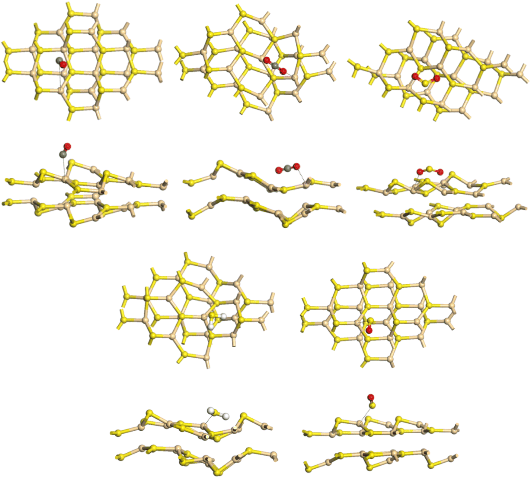 | ||
| Fig. 3 Adsorption systems for gas molecules absorbed on bilayer CdS: optimal adsorption configurations (CO, CO2, SO2, H2S, SO). | ||
E ad of SO2, H2S, and SO adsorbed on the CdS bilayer were (−1.75, −1.69, and −1.92) eV, respectively, and the Q values are (−0.11, −0.16 and −0.21) |e|, respectively. These values indicate charge transfer from CdS bilayer to SO2, H2S, and SO. Their interactions are stronger compared with CO and CO2 on the CdS bilayer. In addition, the sum of the covalent radii of the O and Cd atoms (rO–Cd = 2.24 Å) and the S and Cd atoms (rS–Cd = 2.53 Å) remains smaller than their distance (d = 2.46 Å and d = 2.77 Å). Bonding standards are near the theoretical interatomic covalent radius (±0.3 Å); therefore, chemical bonds can occur in these systems.96 Additionally, after these adsorptions, a significant structural deformation was seen on the CdS bilayer, further proving the strong chemical adsorption between these gas and CdS. The results indicate that the CdS bilayer has excellent application potential as SO2, H2S, and SO sensors with clear sensing responses.97,98 As shown in Fig. 3, the adsorption of these gases on CdS has induced significant changes in atomic positions. The adsorption of CO or SO2 gases on CdS has resulted in considerable structural deformations due to the interaction between the gases and Cd surface atoms. The SO molecule has bound to CdS by interacting with the surface S atom, leading to a vertical displacement of atoms and causing a restructuring of the monolayer. Similarly, H2S has interacted with the surface S atom, and its binding has led to the formation of S–S–H bonds, resulting in alterations in the surface chemistry and atomic arrangement. On the other hand, the CO2 molecule has interacted with the surface S atom, leading to the formation of new bonds and surface reconstruction. These deviations significantly affect the electronic structure, surface chemistry, and sensitivity of CdS, enabling it to detect and discriminate between different gases. Through the study of structural and optical changes induced by gas adsorption, it is possible to design and optimize CdS-based sensors for improved gas sensing performance.
A better understanding of the adsorption behaviours of molecules on the bilayer necessitated a further investigation into the band structures of molecules adsorbed on the CdS bilayer; these results are shown in Fig. 4. The Fermi level is represented by the black dashed line (Ef). After CO, CO2, SO2, and H2S adsorption, the band gap of CdS increased to 2.078, 1.847, 1.712, and 1.890 eV, respectively, while the value of the VBM and CBM remained unaltered at G point. Finally, the adsorption of SO molecules lowered the original band gap (0.95 eV), showing that these adsorptions affect the electronic properties of the CdS bilayer.
 | ||
| Fig. 4 Band structures of bilayer CdS after gas molecules absorption (CO, CO2, SO2, H2S, SO). The red and green lines are referring to the lowest level or edge of the conduction band and the highest level or edge of the valence band, respectively. | ||
To further understand how the adsorption of gas molecules changes the bilayer CdS's electronic properties, we analysed its total and partial densities of states. Fig. 5–9 illustrate the density of states (DOS) and projected density of states (PDOS) for the CdS bilayer adsorption systems. These figures reveal that in the CO/CO2/SO2/H2S–CdS adsorption systems, the DOS undergoes a rightward shift at certain locations. However, in the SO–CdS adsorption system, the DOS exhibits a leftward shift. In the case of theSO adsorption system, the conduction band's bottom shifts to the left, making it easier for the charge to be excited from the valence band to the conduction band.
 | ||
| Fig. 5 DOS and PDOS for CO adsorbed on CdS bilayer. | ||
 | ||
| Fig. 6 DOS and PDOS for CO2 adsorbed on CdS bilayer. | ||
 | ||
| Fig. 7 DOS and PDOS for SO2 adsorbed on CdS bilayer. | ||
 | ||
| Fig. 8 DOS and PDOS for H2S adsorbed on CdS bilayer. | ||
 | ||
| Fig. 9 DOS and PDOS for SO adsorbed on CdS bilayer. | ||
In the case of PDOS, the influence of adsorbed gases on the electronic states near the Fermi energy (Ef) is crucial. The adsorption of CO and CO2 introduces active electronic states in close proximity to Ef. Specifically, in the CO adsorption system, there is an overlap between the s and p orbitals of the Cd atom and the p orbital of the C atom within the energy ranges of 2 to 5 eV and −2 to −5 eV, respectively. Likewise, in the CO2 adsorption system, there is an overlap between the p orbital of the O atom and the s and p orbitals of the Cd atom within the energy ranges of 4 to 6 eV, the s orbital from −2 to −4 eV, and the d orbital from −6 to −9 eV. These overlapping orbitals indicate strong orbital hybridizations, implying the presence of chemical bonding. The electronic densities of SO2, H2S, and SO are all significantly active near Ef, further supporting the existence of chemical bonds with the CdS system. Considering the SO2 adsorption system, the p orbit of the O atom overlaps with the s, p, and d orbits of the Cd atom in the energy range of −2 to −4 eV.
In addition, for the H2S adsorption system, the p orbit of the S atom overlaps with the s and p orbits of the Cd atom in the range of 2 to 12 eV and with the s, p, and d orbits in the range of 0 to −5 eV. Moreover, the s and p orbits of the S atom overlap with the d orbit of Cd in the range of −6 to −8 eV, while the s, p, and d orbits of Cd overlap with the s orbit of the S atom in the range of −10 to −12 eV. For the SO adsorption system, the s and p orbits of the Cd atom overlap with the p orbit of the S atom in the range of 1 to 10 eV and with the s orbit in the range of −9 to −13 eV. Additionally, the s and p orbits of the S atom overlap with the s, p, and d orbits of the Cd atom in the range of 1 to −6 eV, along with the d orbit in the range of −7 to −9 eV. These findings highlight the flexibility and adaptability of CdS to interact with various gas molecules, making it a promising material for potential applications in electronic devices and gas sensing technologies.
By analysing the charge density difference (CDD), the redistribution of charges (ρ) between gas molecules and CdS bilayer has been studied, which is defined as:
| ρ = ρCdS+gas − ρCdS − ρgas, | (3) |
 | ||
| Fig. 10 Electron density difference for bilayer CdS after gas molecules absorption (CO, CO2, SO2, H2S, SO). | ||
The electron localisation function (ELF) was utilised to support the bond in some adsorption models of high adsorption energy and short adsorption distance.99 ELF was found to be a useful tool for thoroughly comprehending the properties of chemical bonds and pairings of non-bond electrons (lone electrons pairs) by defining the amount of electron localisation qualitatively (Fig. 11).89 The ELF value provides an excellent representation of the localisation or delocalisation of electrons between gas molecules and the CdS bilayer.85 As shown in Fig. 6, the ELF of CO and CO2 on the CdS bilayer displays delocalised electrons in the interlayer region. CO and CO2 interact strongly with CdS bilayer. The atoms have still not bonded, though.100
 | ||
| Fig. 11 Slices of electron localisation function for bilayer CdS after gas molecules absorption (CO, CO2, SO2, H2S, SO). | ||
Additionally, this result demonstrates that the gas molecules of CO and CO2 are bound to the CdS bilayer by vdW interactions rather than a chemical bond. When SO2, H2S, and SO are adsorbed on a CdS bilayer, the ELF value in the interlayer areas indicates the establishment of chemical bonds. Considering the substantial ELF plot, quantity of charge transfer, and high adsorption energy, it is shown that ionic bonds, rather than covalent bands, are produced during the adsorption of SO2, H2S, and SO.95 This proves a chemisorption property of the SO2/H2S/SO– CdS system.
3.3 Optical properties of the bilayer CdS-adsorbent systems
It is essential to comprehend the optical properties of 2D materials to determine their potential uses in electrical, optical, and detection systems.98 Throughout the current study, measurements of the bilayer CdS's optical properties were made up to an energy range of about 35 eV. The optical properties of bilayer CdS before and after gas adsorption were studied by calculating their absorption coefficient, refractive index, real (Re) and imaginary (Im) dielectric functions, real conductivity, imaginary conductivity, loss functions, and reflectivity (Fig. 12). | ||
| Fig. 12 Optical properties of bilayer CdS before and after adsorption. | ||
The curves of absorption coefficient (α) of the CdS bilayer before and after adsorption are shown in Fig. 12(a). The pristine bilayer absorption peak is 91682.55 cm−1 at 7.57345 eV. However, the high absorption occurs between 3 and 22 eV, while the edge absorption starts at 0.01 eV (far-IR region) in the pristine CdS bilayer. The absorption coefficients fall within the range of 24070.17 cm−1 to 12684.06 cm−1. Thus, the pristine CdS bilayer can absorb light from the IR to the UV regions, and it can be used in a various applications. It is common knowledge that adsorption causes changes to a material's optical properties. Consequently, it is important to further distinguish the unsatisfactory situation of the adsorption of gas molecules by looking into the considerable alteration of optical properties following the adsorption mechanism.
Moreover, SO/CdS has the highest absorption peak (95523.86 cm−1 at 7.70525 eV), followed by CO (93221.69 cm−1 at 7.60208 eV), H2S (92399.88 cm−1 at 8.19712 eV), SO2 (89072.10 cm−1 at 7.75403 eV) and CO2 (84655.70 cm−1 at 8.19044 eV). Notably, the gas molecules adsorbed on the CdS bilayer cause the UV absorption peak to rise compared to the peak of the pristine bilayer. As shown from the above result, the molecules adsorbed on the CdS bilayer are useful in UV-sensitive optoelectronic and photoelectric devices. Fig. 12(b) shows the refractive index curves for pristine CdS bilayer and adsorption gas. For pristine CdS, the maximum refraction index value is 1.9286 at 1.38763 eV. Following gas adsorption, the refractive index decreases as photon energy increases, settling at a roughly constant value of 0.96 at around 30 eV. The maximum refractive index is for H2S (1.87142), followed by CO2/CdS (1.83241), and then CO (1.81326), SO (1.81236), and SO2 (1.80687), respectively. By summing the real and imaginary components, we will get the dielectric function, which appears like the below:101,102
| ε(ω) = ε1(ω) + iε2(ω) | (4) |
 | (5) |
 | (6) |
Moreover, multiple peaks are observed in the adsorption systems with gas molecules (Fig. 12(c)). These dielectric function curves vary, but at an energy of 29 eV, they approach and remain fixed. When compared to the pristine bilayer's peak, the imaginary dielectric function exhibits the same behaviour as its real component equivalent, with the number of peaks increasing and the maximum peak value decreasing. The H2S molecule possessed the highest peak of the imaginary dielectric function, which equals 3.35205 at 3.10738 eV.
The real and imaginary conductivity curves of the pristine CdS bilayer and the adsorption gas are shown in Fig. 12(e) and (f). The maximum real conductivity of the pristine CdS bilayer is 1.56319 at an energy of 5.76363 eV, which lies in the UV region. Conductivity gradually decreases after the gas molecules adsorption on CdS bilayer.
Where (1.55137) is the highest value for the conductivity of the gas SO, followed by CO (1.52149), H2S (1.46892), CO2 (1.42478), and SO2 (1.40284), respectively. For the imaginary conductivity of the pristine CdS bilayer, The maximum peak is 0.77882 at an energy of 8.14071 eV, and it lower once gas molecules are adsorbed on it.
The loss function curves for a pristine CdS bilayer and adsorption gas as a function of photon energy are shown in Fig. 12(g). The curve of the pristine CdS bilayer exhibits a noticeable peak with a value of 1.11924 at an energy of 8.762 eV, which is in the UV region. Compared to the pristine bilayer's peak, all molecules adsorbed on the CdS bilayer exhibit higher peaks.
The curves of CdS bilayer reflectivity before and after adsorption is shown in Fig. 12(h). Two lower peaks for the pristine CdS bilayer were found at 5.95271 eV (0.13493) and 3.62965 eV (0.12175). In addition, the higher peak lies at 7.73553 eV (0.13518) in the UV region. As gas molecules are absorbed, the maximum reflection peak values rise. The UV region is still displaying large peaks at this time.
3.4 Recovery time
A crucial parameter of any gas sensor is the recovery time, namely the time for gas desorption from the adsorbed surface. For application purposes, a gas sensor has to be frequently reusable. Hence, the material used in the sensor should demonstrate the property of a low recovery time. The recovery time, the key performance of a gas sensor associated with the desorption sensing mechanism, is determined using the transition state theory as:103,104 | (7) |
4. Conclusions
Density functional theory calculations were employed to investigate the adsorption behavior of toxic gas molecules, namely CO, CO2, SO2, H2S, and SO, on the CdS bilayer. The aim was to assess the feasibility of utilising CdS bilayers as gas sensors for detecting these gases. The results revealed that the interaction between SO2, H2S, and SO with the bilayer CdS is stronger compared to CO and CO2. Moreover, while CO2 and CO exhibited physisorption on the CdS bilayer, the other molecules (SO2, H2S, and SO) demonstrated chemisorption with shorter distances and higher adsorption energies. The adsorption of gas molecules induced significant changes in the electronic properties of the CdS bilayer, particularly in the total and partial density of states. The optical properties analysis indicated that the adsorption of gas molecules altered the absorption coefficient, refractive index, real (Re) and imaginary (Im) dielectric functions, real conductivity, imaginary conductivity, loss functions, and reflectivity of the CdS bilayer. Notably, the adsorption of gas molecules enhanced the CdS bilayer's light absorption in the UV range. These findings highlight the excellent performance of the CdS bilayer as a gas sensor for gases such as SO2, H2S, and SO.Data availability
All data and materials are provided in the main manuscript.Author contributions
Abbas H. Abo Nasria designed the research project and supervised the work and Warood Kream Alaarage carried out the calculations. All authors contributed to data interpretation and discussion of the results.Conflicts of interest
There are no conflicts to declare.In addition, Q of the CO and CO2 adsorption systems are (0.02 and −0.02) |e|, respectively; this indicates that charges are transferred from the CdS bilayer to the CO2, whereas for CO, which is the opposite. However, the covalent radii of the C and Cd atoms (rC–Cd = 2.28 Å) and the O and Cd atoms (rO–Cd = 2.24 Å) are both smaller than the calculated adsorption distance,81 confirming the existence of a weak van der Waals force between the CdS bilayer and the gas molecules.95
Acknowledgements
We acknowledge Kufa University.References
- M. D. Ganji, S. Jameh-Bozorgi and M. Rezvani, Appl. Surf. Sci., 2016, 384, 175 CrossRef CAS.
- N. Ahmadian, M. D. Ganji and M. Laffafchy, Mater. Chem. Phys., 2012, 135, 569 CrossRef CAS.
- J. P. Boudou, M. Chehimi, E. Broniek, T. Siemieniewska and J. Bimer, Carbon N. Y., 2003, 41, 1999 CrossRef CAS.
- J. Wang, H. Yi, X. Tang, S. Zhao and F. Gao, Chem. Eng. J., 2020, 384, 123334 CrossRef CAS.
- Z. Zhao, Y. Yong, Q. Zhou, Y. Kuang and X. Li, ACS Omega, 2020, 5, 12364 CrossRef CAS PubMed.
- M. I. Khan, M. Hassan, A. Majid, M. Shakil and M. Rafique, Appl. Surf. Sci., 2023, 616, 156520 CrossRef CAS.
- K. S. Novoselov, A. K. Geim, S. V. Morozov, D. Jiang, Y. Zhang, S. V. Dubonos, I. V. Grigorieva and A. A. Firsov, Science, 2004, 306, 666 CrossRef CAS.
- S. Cahangirov, M. Topsakal, E. Aktürk, H. Šahin and S. Ciraci, Phys. Rev. Lett., 2009, 102, 236804 CrossRef CAS PubMed.
- Q. Peng, X. Sun, H. Wang, Y. Yang, X. Wen, C. Huang, S. Liu and S. De, Appl. Mater. Today, 2017, 7, 169 CrossRef.
- M. Isa Khan, I. Ashfaq, A. Majid, M. Shakil and N. ul ain, Mater. Chem. Phys., 2023, 295, 127174 CrossRef CAS.
- T. Banibairami, S. Jamehbozorgi, R. Ghiasi and M. Rezvani, Russ. J. Phys. Chem. A, 2020, 94, 581 CrossRef CAS.
- Y. Wu, X. Zhang, A. Negi, J. He, G. Hu, S. Tian and J. Liu, Polymers, 2020, 12, 426 CrossRef CAS.
- T. Chen, X. Meng, R. Jiang, J. Liang, Q. Yang, Q. Tan, C. Sun, X. Zhang and S. Ren, Phys. Chem. Chem. Phys., 2016, 18, 16302 RSC.
- H. R. Jappor and A. S. Jaber, Sens. Lett., 2016, 14, 989 CrossRef.
- H. R. Jappor, Phys. B Condens. Matter, 2017, 524, 109 CrossRef CAS.
- J.-B. Wang, X. Cheng, Z. Xu, K. Tsang and H. Ki Xu, Nat. Photonics, 2013, 7, 888 CrossRef.
- J. Li, C. Yang, S. Li, S.-S. Xia and J.-B. Li, J. Phys. Chem. C, 2013, 117, 483 CrossRef.
- J. Wang, J. Meng, J. Li and Q. Yang, Phys. Chem. Chem. Phys., 2016, 18, 17029 RSC.
- V. Nagarajan, R. Nivedhana and R. Chandiramouli, Inorg. Chem. Commun., 2023, 152, 110683 CrossRef CAS.
- V. Nagarajan, R. Bhuvaneswari and R. Chandiramouli, J. Mol. Graph. Model., 2023, 121, 108449 CrossRef CAS PubMed.
- Y. Ma, D. Zhang, J. Li, X. He, C. Lu, Z. Lu, Z. Yang and Z. Wang, Sens. Actuators, B, 2018, 266, 664 CrossRef.
- S. Zhu and S. Ma, Appl. Sci., 2019, 9(11), 2390 CrossRef.
- J.-M. Chen, G.-X. Li, H.-F. Wang, D.-D. Li, Si-Qi Fan and X.-Bo Zhang, Vacuum, 2019, 165, 35 CrossRef.
- C. Gao, Y. Zhang, H. Yang, Y. Liu, Y. Liu, J. Du, H. Ye and G. Zhang, Appl. Surf. Sci., 2019, 494, 162 CrossRef CAS.
- J. A. Shlaka and A. H. Abo Nasria, IOP Conf. Ser. Mater. Sci. Eng., 2020, 928, 072082 CrossRef CAS.
- Y. Wang, N. Song, X. Song, T. Zhang, D. Yang and M. Li, Vacuum, 2018, 147, 18 CrossRef CAS.
- T. A. Hussein, W. K. Alaarage, H. A. Abdulhussein, N. Seriani and A. H. Abo Nasria, Comput. Theor. Chem., 2023, 1223, 114086 CrossRef CAS.
- Y. Jappor, H. Rahman Obeid, M. M. Vu, T. V. Hoat, D. M. Bui, H. D. Hieu, Nguyen N. Edrees, Shaker J. Mogulkoc and R. Khenata, Superlattices Microstruct., 2019, 130, 545 CrossRef.
- T. Alaa Hussein, N. M. Shiltagh, W. Kream Alaarage, R. R. Abbas, R. A. Jawad and A. H. Abo Nasria, Results Chem., 2023, 5, 100978 CrossRef CAS.
- T. A. Hussein, W. K. Alaarage, H. A. Abdulhussein, N. Seriani and A. H. Abo Nasria, Comput. Theor. Chem., 2023, 1223, 114086 CrossRef CAS.
- A. H. A. Nasriya and J. Eng, Appl. Sci., 2018, 13, 89 Search PubMed.
- H. R. Jappor and M. A. Habeeb, Phys. E, 2018, 101, 251 CrossRef CAS.
- M. S. Jyothi, V. Nagarajan and R. Chandiramouli, Mol. Phys., 2023, 121(5), e2184655 CrossRef.
- K. D. Pham, T.-D. Hoang, Q.-T. Nguyen and D.-Q. Hoang, J. Alloys Compd., 2023, 940, 168919 CrossRef CAS.
- M. D. Ganji and M. Rezvani, J. Mol. Model., 2013, 19, 1259 CrossRef CAS.
- W. Kream Alaarage, A. H. Abo Nasria and A. H. Omran Alkhayatt, Comput. Theor. Chem., 2023, 1227, 114223 CrossRef CAS.
- V. Chandiramouli and R. Nagarajan, Vacuum, 2017, 142, 13 CrossRef.
- F. Niu, M. Cai, J. Pang, X. Li, D. Yang and G. Zhang, Vacuum, 2019, 168, 108823 CrossRef CAS.
- H. Xia, J. Peng, K. Liu, C. Li and Y. Fang, J. Phys. D Appl. Phys., 2008, 41, 105405 CrossRef.
- L. Yadava, R. Verma and R. Dwivedi, Sens. Actuators, B, 2010, 144, 37 CrossRef CAS.
- D. S. Dhawale, D. P. Dubal, V. S. Jamadade, R. R. Salunkhe, S. S. Joshi and C. D. Lokhande, Sens. Actuators, B, 2010, 145, 205 CrossRef CAS.
- X. Fu, J. Liu, Y. Wan, X. Zhang, F. Meng and J. Liu, J. Mater. Chem., 2012, 22, 17782 RSC.
- B. T. Raut, P. R. Godse, S. G. Pawar, M. A. Chougule and V. B. Patil, J. Mater. Sci. Mater. Electron., 2012, 23, 956 CrossRef CAS.
- T. Arai, T. Yoshida and T. Ogawa, Jpn. J. Appl. Phys., 1987, 26, 396 CrossRef CAS.
- B. Su and K. L. Choy, Thin Solid Films, 2000, 359, 160 CrossRef CAS.
- H. H. Afify and I. K. Battisha, J. Mater. Sci.: Mater. Electron., 2000, 11, 373–377 CrossRef CAS.
- R. Demir, S. Okur and M. Şeker, Ind. Eng. Chem. Res., 2012, 51, 3309 CrossRef CAS.
- S. T. Navale, A. T. Mane, M. A. Chougule, N. M. Shinde, J. Kim and V. B. Patil, RSC Adv., 2014, 4, 44547 RSC.
- Y. Cao, L. Guo, M. Dan, D. E. Doronkin, C. Han, Z. Rao, Y. Liu, J. Meng, Z. Huang, K. Zheng, P. Chen, F. Dong and Y. Zhou, Nat. Commun., 2021, 12, 1675 CrossRef CAS.
- J. Zhai, L. Wang, D. Wang, H. Li, Y. Zhang, D. Qing He and T. Xie, ACS Appl. Mater. Interfaces, 2011, 3, 2253 CrossRef CAS.
- N. A. Noor, N. Ikram, S. Ali, S. Nazir, S. M. Alay-E-Abbas and A. Shaukat, J. Alloys Compd., 2010, 507, 356 CrossRef CAS.
- E. H. Atmani, I. Bziz, N. Fazouan and M. Aazi, Appl. Phys. A, 2021, 127, 878 CrossRef CAS.
- Y. Wang, in Int. Conf. Optoelectron. Inf. Funct. Mater. (OIFM 2022), ed. C. Zuo, SPIE, 2022, p. 56 Search PubMed.
- J. Jia, Y. Zhang, W. Yan, X. Guo, T. Fan, Y. Ni, L. Weng, Y. Zha, Z. Liu, J. Tian, L. Li and T. Duan, J. Alloys Compd., 2020, 832, 154965 CrossRef.
- M. Zafar, M. Shakil, S. Ahmed, M. Raza-ur-rehman Hashmi, M. A. Choudhary and Naeem-ur-Rehman, Sol. Energy, 2017, 158, 63–70 CrossRef CAS.
- B. Sharma, R. Lalwani and R. Das, Optik, 2023, 281, 170831 CrossRef CAS.
- M. A. Mahdi, Z. Hassan, S. S. Ng, J. J. Hassan and S. K. M. Bakhori, Thin Solid Films, 2012, 520, 3477 CrossRef CAS.
- A. S. Obaid, M. A. Mahdi, Z. Hassan and M. Bououdina, Superlattices Microstruct., 2012, 52, 816 CrossRef CAS.
- S. K. J. A.-A. l-Ani, M. A. Mahdi, S. J. Kasem1, J. J. Hassen1 and A. A. Swadi, Int. J. Nanoelectron. Mater., 2009, 41–52 Search PubMed.
- D. Shvydka, J. Drayton, A. D. Compaan and V. G. Karpov, Appl. Phys. Lett., 2005, 87, 123505 CrossRef.
- C. Zhu, L. Feng, D. Li, F. Zhang, Y. Li, C. Wang, Y. Lin, Z. Ruan and S. Chen, RSC Adv., 2014, 4, 61691 RSC.
- V. Smyntyna, V. Golovanov, S. Kačiulis, G. Mattogno and G. Righini, Sens. Actuators B, 1995, 25, 628 CrossRef CAS.
- V. L. Colvin, M. C. Schlamp and A. P. Alivisatos, Nature, 1994, 370, 354 CrossRef CAS.
- J. L. Rejon, V. Riech, I. Hernandez-Rodriguez, E. Quintana and P. Pena, in IEEE 40th Photovolt. Spec. Conf., IEEE, 2014, pp. 1696–1698 Search PubMed.
- D. K. Biswas, A. Meher and S. R. Kaushik, J. Phys. Conf. Ser., 2022, 2267, 012155 CrossRef.
- A. A. Al-Zahrani, J. Ouerfelli, A. M. Holi and N. Ouerfelli, Optik, 2023, 274, 170584 CrossRef CAS.
- A. Fabbri, B. Gaiardo, A. Guidi, V. Malagù and C. Giberti, Procedia Eng., 2014, 87, 140 CrossRef.
- U. Deb, J. Majidi and R. Sarkar, ACS Appl. Opt. Mater., 2022 Search PubMed.
- P. Frondelius, H. Häkkinen and K. Honkala, New J. Phys., 2007, 9, 339 CrossRef.
- H. A. Hussein, M. Gao, Y. Hou, S. L. Horswell and R. L. Johnston, Z. Phys. Chem., 2019, 233, 813 CrossRef CAS.
- H. A. Hussein, J. B. A. Davis and R. L. Johnston, Phys. Chem. Chem. Phys., 2016, 18, 26133 RSC.
- A. F. Qasrawi and T. Y. Abed, Thin Solid Films, 2019, 679, 72 CrossRef CAS.
- R. Zhou, H. Niu, Q. Zhang, E. Uchaker, Z. Guo, L. Wan, S. Miao, J. Xu and G. Cao, J. Mater. Chem. A, 2015, 3, 12539 RSC.
- C. M. Marian, A. Heil and M. Kleinschmidt, Wiley Interdiscip. Rev. Comput. Mol. Sci., 2019, 9(2), e1394 CrossRef.
- J. P. Perdew, K. Burke and M. Ernzerhof, Phys. Rev. Lett., 1996, 77, 3865 CrossRef CAS PubMed.
- N. Mardirossian and M. Head-Gordon, Phys. Chem. Chem. Phys., 2014, 16, 9904 RSC.
- J. Chen, L. Jia, X. Cui, W. Zeng and Q. Zhou, Mater. Today Chem., 2023, 28, 101382 CrossRef CAS.
- M. M. Obeid, H. R. Jappor, S. J. Edrees, M. M. Shukur, R. Khenata and Y. Mogulkoc, J. Mol. Graph. Model., 2019, 89, 22 CrossRef CAS.
- M. Ernzerhof and G. E. Scuseria, J. Chem. Phys., 1999, 110, 5029 CrossRef CAS.
- Q. Yue, Z. Shao, S. Chang and J. Li, Nanoscale Res. Lett., 2013, 8(1), 425 CrossRef.
- P. Pyykkö and M. Atsumi, Chem.–Eur. J., 2009, 15, 186 CrossRef.
- X.-P. Yang, Q. Chen, J.-K. Meng, R.-S. Jiang, T.-L. Liang, Q.-H. Tan, C.-J. Cai, M. Sun, X. Yang and D.-G. Ren, IEEE Electron Device Lett., 2016, 37, 660 Search PubMed.
- P. J. D. Segall, M. D. Lindan, C. J. Probert, M. J. Pickard, M. C. Hasnip, P. J. Clark and S. J. Payne, J. Phys. Condens. Matter, 2002, 14, 2717 CrossRef.
- X. Obeid, M. M. Shukur, M. M. Edrees, S. J. Khenata, R. Ghebouli, M. A. Khandy, S. Ahmad Bouhemadou, A. Jappor and H. Rahman Wang, Chem. Phys., 2019, 526, 110414 CrossRef.
- X. Sun, X. Yang, Q. Meng, R. Tan, C. Liang, Q. Jiang, J. Ye and H. Chen, Appl. Surf. Sci., 2017, 404, 291 CrossRef CAS.
- J. Heyd, G. E. Scuseria and M. Ernzerhof, J. Chem. Phys., 2003, 118, 8207 CrossRef CAS.
- A. R. Villegas and C. E. P. Rocha, J. Phys. Chem. C, 2015, 119, 11886 CrossRef.
- H. R. Jappor, Z. A. Saleh and M. A. Abdulsattar, Adv. Mater. Sci. Eng., 2012, 2012, 1–6 CrossRef.
- X. Sun, Y. Guo, Y. Zhao, S. Liu and H. Li, Sensors, 2020, 20, 2879 CrossRef CAS.
- A. Rahmanzadeh, M. Rezvani, M. Darvish Ganji and M. Tale Moghim, Mater. Today Commun., 2023, 36, 106946 CrossRef CAS.
- H. Pasdar, N. Elmi Fard and M. Rezvani, Appl. Phys. A, 2023, 129, 380 CrossRef CAS.
- D. Lichuan, X. Zhou, Y. Jie and L. Wang, J. Electron. Mater., 2022, 51, 7297 CrossRef CAS.
- B. Gergen, H. Nienhaus, W. H. Weinberg and E. W. McFarland, Science, 2001, 294, 2521 CrossRef CAS.
- R. Q. Wu, M. Yang, Y. H. Lu, Y. P. Feng, Z. G. Huang and Q. Y. Wu, J. Phys. Chem. C, 2008, 112, 15985 CrossRef CAS.
- X.-P. Meng, R.-S. Cai, M. Jiang, J.-K. Liang, Q.-H. Sun, X. Yang, Q. Tan and C.-J. Chen, IEEE Electron Device Lett., 2017, 38, 134 Search PubMed.
- C. Yongqing, K. Qingqing, Z. Gang and Z. Yong-Wei, J. Phys. Chem. C, 2015, 119, 3102 CrossRef.
- F. M. Berdiyorov, G. R. Neek-Amal, M. Hussein, I. A. Madjet and M. E. Peeters, J. Mater. Chem. A, 2017, 5, 2110 RSC.
- E. P. Wu, L. Chu, H. S. Koh and W. S. Li, Opt. Express, 2010, 18, 14395 CrossRef.
- J. Jin, Y. Li and X. Yang, Phys. Chem. Chem. Phys., 2015, 17, 18665 RSC.
- G. Liu, L. Yang, Q. Wang, Z. Ye, H. Chen, X. Fan and X. Zhang, Appl. Surf. Sci., 2018, 433, 575 CrossRef.
- H. Tributsch, Z. Naturforsch. A, 1977, 32, 972 Search PubMed.
- H. R. Jappor and M. A. Habeeb, Curr. Appl. Phys., 2018, 18, 673 CrossRef.
- Y. Yong, F. Ren, Z. Zhao, R. Gao, S. Hu, Q. Zhou and Y. Kuang, Appl. Surf. Sci., 2021, 551, 149383 CrossRef CAS.
- D. G. Truhlar and B. C. Garrett, Acc. Chem. Res., 1980, 13, 440 CrossRef CAS.
- S. Peng, K. Cho, P. Qi and H. Dai, Chem. Phys. Lett., 2004, 387, 271 CrossRef CAS.
| This journal is © The Royal Society of Chemistry 2024 |