DOI:
10.1039/D4RA00031E
(Paper)
RSC Adv., 2024,
14, 17238-17244
Interfacial electronic state between hexagonal ZnO and cubic NiO
Received
2nd January 2024
, Accepted 22nd April 2024
First published on 28th May 2024
Abstract
The interface of two dissimilar materials gives rise to a myriad of interesting structural, magnetic, and electronic properties that may be utilized to produce novel materials with unique characteristics and functions. In particular, growing a cubic oxide film on top of a hexagonal oxide substrate results in such unique properties due to the conflict of their respective stabilization mechanisms within the interface layer. This study aims to elucidate the electronic properties of the interface between hexagonal ZnO and cubic NiO by analyzing the interface electronic states within epitaxial NiO films grown on ZnO substrates, expressed in the form of ultraviolet photoemission spectroscopy (UPS) for valence band structure and X-ray absorption spectroscopy (XAS) spectra for conduction band structure. This is accomplished through a modeling approach in which the film, substrate, and interface signals are assumed to be related to each other by a set of mathematical equations, and then rearranging and modulating the equations to obtain unique UPS and XAS spectra that depict the interface electronic states.
Introduction
In the ever-evolving sector of device fabrication, there is continuing need for a deeper understanding of how different materials interact. One point of scrutiny is the interface between two or more different functional materials. Heteroepitaxy between dissimilar materials give rise to a variety of fascinating properties due to the conflict of stabilization mechanisms within the interfacial layers.1 Such interfaces often exhibit structural, optical, magnetic, and electronic properties that are different relative to their individual counterparts, and there exists considerable interest in regards to how these properties may be exploited to realize material combinations that perform synergistically in real-life applications such as catalysis, plasmonics, and electronics.2,3
The interface electronic states of a NiO/ZnO heterostructure is studied in this work. ZnO is hexagonal wurtzite, and exhibits a bandgap of 3.37 eV and exciton binding energy of 60 meV at room temperature. It is suitable for a multitude of modern functional devices such as detectors, optical sensors, light-emitting diodes (LEDs).4–7 ZnO nanofilms are also expected to be promising thermoelectrics8 and catalysts for efficient hydrogen reaction.9 However, stable p-type ZnO thin films exhibit self-compensation due to a large concentration of background n-type carriers.10,11 Alternative p-type oxides such as NiO have been studied. Cubic NiO has high stability and reproducibility, with stable chemical properties, a bandgap of 3.7 eV, and exceptional optical, magnetic, and electrical properties. As such, it is seen as a suitable alternative to p-type ZnO.1 Furthermore, several p-NiO/n-ZnO heterojunction-based optoelectronic devices such as LEDs and ultraviolet detectors have been fabricated.12–16 Studies on the interfacial electronic structure such as the band offset of NiO/ZnO heterojunctions have been conducted,17–19 yet there is still a need to further elucidate the intrinsic electronic properties at the NiO–ZnO interface. A prominent way of studying heterojunction interfaces is via growth of epitaxial thin films, where the growth process is carefully controlled and monitored, with various measurement techniques being used at set intervals throughout the growth process to record and study interesting properties.1,20–24
To date, detailed study of the electronic structure within nanoscale thin films have mostly been conducted via surface-sensitive techniques such as ultraviolet photoelectron spectroscopy (UPS), X-ray absorption spectroscopy (XAS), and X-ray photoelectron spectroscopy (XPS). Despite their established reliability, these methods are not optimal when it comes to examining the electronic states at heterojunction interfaces, due to limitations of their electron mean free paths and difficulty in decoupling the electronic states of the interface from that of other non-interface phases. Electron microscopy techniques such as electron energy loss spectroscopy (EELS) and scanning transmission electron microscopy (STEM) can be useful in probing the functional interfaces of thin films, but are nevertheless expensive and time-consuming to conduct.25
One interesting method that addresses some of these issues has been proposed in the study of Wang et al.,20 which uses a mathematical model to simulate and extract the interface electronic states from the UPS spectra of a CoO/Fe3O4 heterostructure. It first assumes that the density of states in a theoretical perfect epitaxial film is completely independent of its substrate, i.e. the UPS spectra consists of the superposition of only the signal from the substrate and bulk film, and no interfacial states are present. If the experimental spectra exhibit any major deviation from these theoretical spectra, then unique interfacial states are inferred to exist. The interfacial states can then be found by solving for a set of equations that relate multiple key parameters, including the substrate, film, and interface states.
This study employs a similar method to extract the interface states of a NiO/ZnO heterostructure from the existing UPS spectra, and also extends the method to the XAS spectra that have not been applied to previously. The experimental data used are based on the report by Li et al.,1 in which the UPS and XAS spectra were obtained throughout the growth of NiO films with different thickness on the ZnO substrate along the [0001] direction. The study inferred the existence of interface states in the valence band via analysis of the UPS spectra, but the interface states were not thoroughly quantified and studied in detail. On the other hand, no similar analysis was done toward the XAS spectra to account for the interface states in the conduction band. Therefore, this study aims to unravel the interface electronic states of the NiO/ZnO system by employing the modeling technique from Wang et al.20 to simulate and extract the interface states within the valence and conduction band, based on the UPS and XAS spectra from the report by Li et al.,1 respectively. Furthermore, we attempt to determine the extent of the contribution of both substrate and film to the interface states by proposing a few variants for the models with interface states and determining the most optimal thickness for both substrate and film that are contributed to the interface structure, respectively.
Methodology
The experimental UPS and XAS spectra of the NiO/ZnO are extracted from the report by Li et al.1 The NiO films were epitaxially grown on a ZnO substrate using molecular beam epitaxy (MBE), and the structural and electronic properties of the film were characterized using X-ray diffraction (XRD), electron energy loss spectroscopy (EELS), scanning transmission electron microscopy (STEM), UPS, and XAS. UPS and XAS are surface-sensitive techniques,25,26 which makes it difficult to directly investigate the embedded interface electronic states. However, it is possible to characterize the interfacial electronics states by observing and analyzing the spectral trends throughout the NiO film growth, assuming layer-by-layer growth. Next, we attempt to use modeling techniques on the NiO/ZnO system to evaluate two assumptions, i.e. the system is either with or without interfacial electronic states.
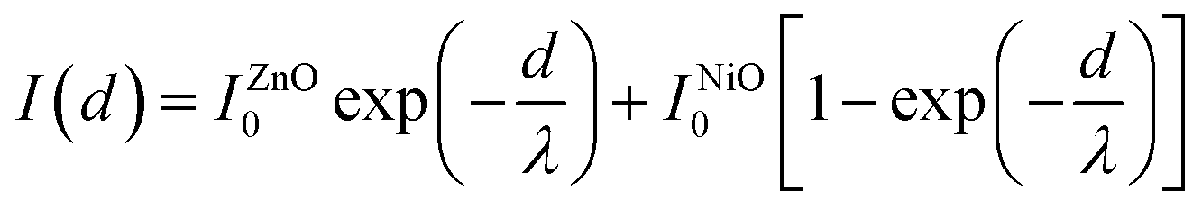
UPS modeling without interface states
Given that a UPS spectrometer probes the film down to a few monolayers below the surface of a sample, the resulting UPS spectrum of any ultrathin film grown on a substrate will be a superposition of emissions from the film, substrate, and any interfacial states that may be present in between, with each parameter weighted by electron escape depths. A model of a UPS spectrum without interfacial states, expressed as the spectral intensity I as a function of film thickness d, is constructed using the formula,| |
 | (1) |
where IZnO0 and the INiO0 are the bulk UPS spectra of the ZnO substrate and NiO film, respectively; d is the film thickness grown on the substrate, and λ is the inelastic mean free path. Any discrepancy between the measured and model spectra are assumed to be a result of interface electronic states. Hence, the difference between each experimental spectrum and its corresponding model spectrum is obtained.
UPS modeling with interfacial electronic states
We first gauge the presence of interfacial electronic states and determine the extent of their influence across the NiO/ZnO interface. This is done by taking the sequential UPS spectrum with each interval of NiO film deposition to separate out the electronic structure of each NiO layer by subtracting the signal contributed by the background, ZnO substrate, and NiO layers underneath from the experimental spectrum of a particular interval of time during which NiO is being deposited. The sequential UPS spectrum at each time interval is obtained via the formula,| |
I(j−i)th = Ij − Ii![[thin space (1/6-em)]](https://www.rsc.org/images/entities/char_2009.gif) exp(−d(j−i)th/λ) exp(−d(j−i)th/λ)
| (2) |
where Ij denotes the spectral intensity of a j nm-thick sample, and Ii denotes the intensity of a i nm-thick sample. I(j−i) yields the intensity of the topmost layer of (j − i) nm thickness at any given time, obtained by subtracting the Ii from Ij, corrected for attenuation due to the (j − i)th layer with thickness d(j−i)th and the electron escape depth, hence the coefficient exp(−d(j−i)th/λ).
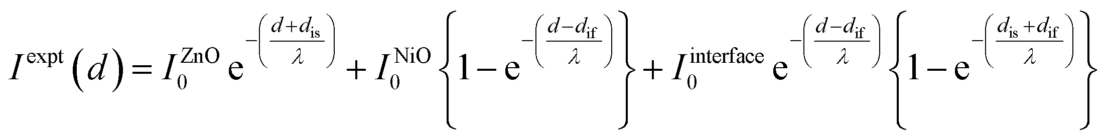
We then use a model that relates the NiO film, ZnO substrate, and interfacial states to one another via an equation. This model builds upon eqn (1) by introducing two variables that account for the interface states contributed by the substrate and film toward the experimental UPS spectra.
| |
 | (3) |
where
Iinterface0 is the interfacial state spectrum,
dif is the thickness of the film-side interfacial layer, and
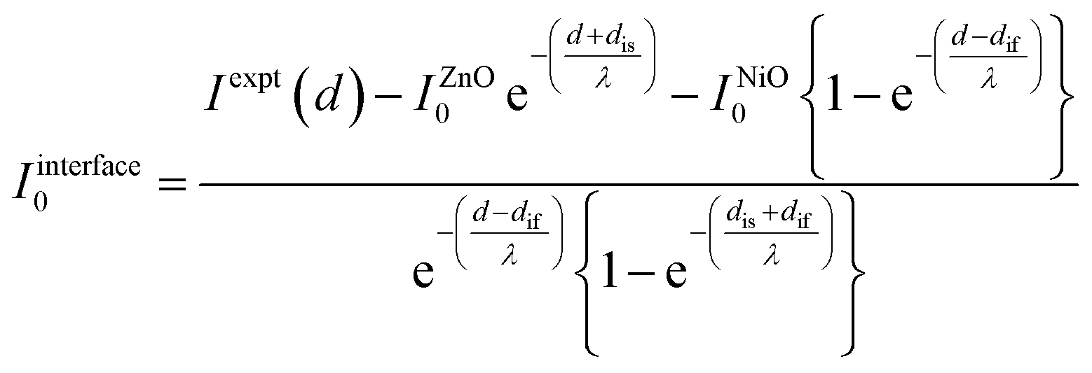
dis is thickness of the substrate-side interfacial layer. The interfacial state spectrum can then be acquired by solving for
Iinterface0.
| |
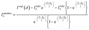 | (4) |
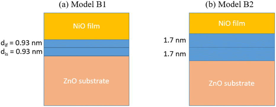
Throughout the film growth in the report by Li et al.,1 an interfacial layer extending up to 1.7 nm was observed via scanning transmission electron microscopy (STEM). We thus consider two variants of the same model derived from eqn (4) – one assumes that interface states are contributed solely by the film (Model A), i.e. dis = 0; the other assumes that both film and substrate equally contribute to the interfacial layer (Model B) (Fig. 1).
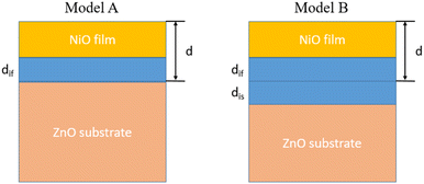 |
| | Fig. 1 Two models to evaluate the interfacial states. Model A assumes that only the film contributes to the interfacial states; Model B assumes that both the film and substrate contribute to the interfacial states. | |
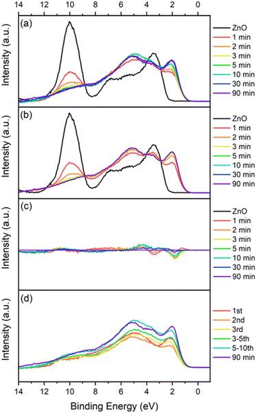
Ideally for our model, the closer we get to the true value of dis and/or dif, the smaller the variation of the interfacial state spectrum determined from the experimental spectra across the range of d that exhibits the possible presence of interface states. We highlight this by investigating two variants for both Model A and B. For Model A, one variant has its d set to 0.93 nm due to it being the smallest thickness measured during film growth in the report by Li et al.1 The other has its d set to 1.7 nm due to the formation of an interfacial layer observed in the report by Li et al.1 that extends up to 1.7 nm (Fig. 2).
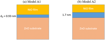 |
| | Fig. 2 Two variants of Model A were inspected in this study. Apart from dif, the values remain the same for the remaining parameters. 0.93 nm was chosen as the dif in (a); 1.7 nm was chosen as the dif in (b). | |
Next, we consider the possibility of interface states extending to the ZnO substrate (Fig. 3). For simplicity, we assume that dis = dif.
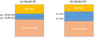 |
| | Fig. 3 Two variants of Model B were inspected in this study. Apart from dis and dif, the values remain the same for the remaining parameters. The setup is similar to Fig. 2, albeit this time with the inclusion of dis below the dif component that shares the same value with dif i.e. (a) dis = dif = 0.93 nm, (b) dis = dif = 1.7 nm. | |
Assessment of model consistency via a similarity factor
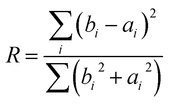
For each model, interfacial state spectra were generated for d = 0.93 nm and d = 1.66 nm, respectively, due to these values being within the confines of the thickness of the 1.7 nm interfacial layer. Similarity testing for both spectra was conducted via a reliability factor (R factor), defined as| |
 | (5) |
where ai and bi are the interface signals for d = 0.93 nm and 1.66 nm, respectively. A lower R factor indicates greater similarity.
All the steps above were repeated for the XAS spectra extracted from the report by Li et al.1
Results and discussion
Ultraviolet photoelectron spectroscopy (UPS)
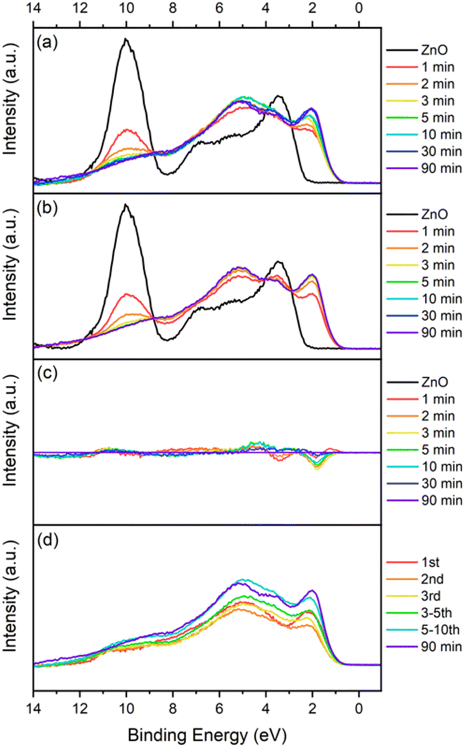
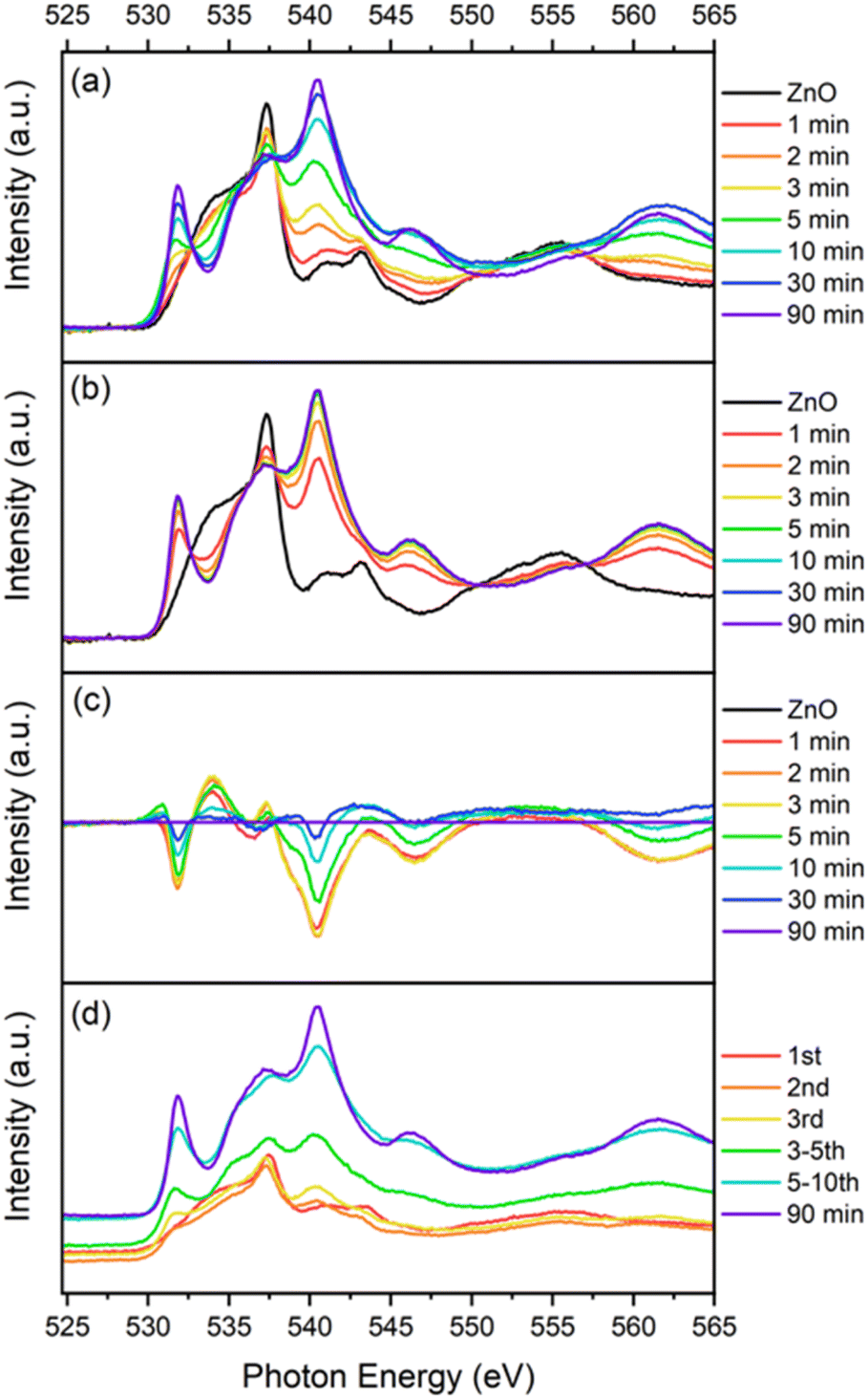
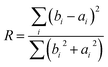
The experimental data in Fig. 4(a) were obtained from the report by Li et al.1 The peaks of the experimental UPS spectrum of the 90 min NiO film exhibit similarities to that of single-crystal NiO in the study of Mckay et al.,27 and is thus taken to be the bulk NiO spectrum, INiOO. Similarly, the experimental UPS spectrum of the ZnO (0001) substrate contains peaks similar to that of single-crystal ZnO shown in the study of Solomon et al.,28 most notably the Zn 3d and O 2p peaks. Hence, the ZnO spectrum is taken as the bulk ZnO spectrum, IZnOO. Fig. 4(b)–(d) were successfully reproduced using the corresponding equations, i.e. (b) was obtained using eqn (1); (c) was obtained by subtracting (b) from (a); (d) was obtained using eqn (2). According to Li et al.,1 the presence of significant dissimilarities between the experimental and model spectra – in this case, the troughs in the spectra ranging from 1 min to 10 min in Fig. 4(c) – suggests the possible presence of interfacial electronic states at the valence band due to the discrepancy between experiment and model spectra.
 |
| | Fig. 4 (a) Experimental UPS spectra of NiO films of different thicknesses grown on ZnO (reproduced with permission from the report by Li et al.1). The ZnO spectrum has been shifted to the right by 0.8 eV to align its Zn 3d peak with the left peak of 1 min NiO deposition. The inelastic Li–Henrich background has been subtracted from each spectrum. (b) Model UPS spectra obtained via eqn (1). (c) Difference spectra obtained by subtracting the model spectra from the experimental spectra. (d) Sequential difference of each deposition interval obtained using eqn (2). | |
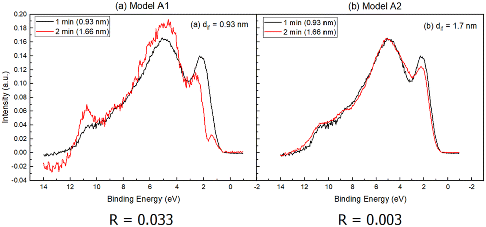
According to the assumption in eqn (4), the interfacial state spectrum for a fixed dis and dif should be identical within a certain range of d, where d ≤ 1.7 nm. Hence, error analysis via R factor was used to quantify the similarity between the interface signal at 1 and 2 min, i.e. when d = 0.93 nm and 1.66 nm, respectively.1
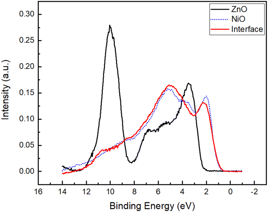
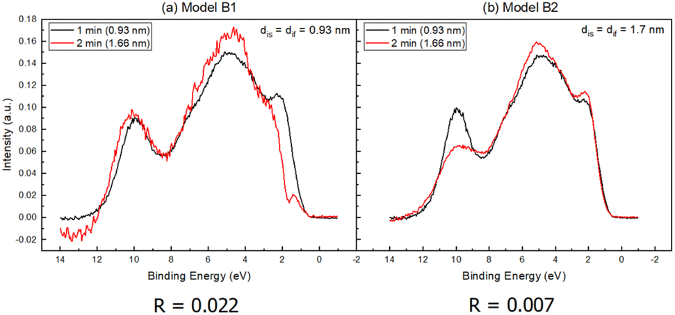
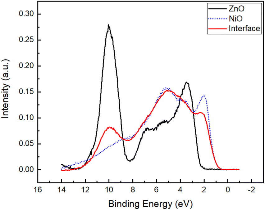
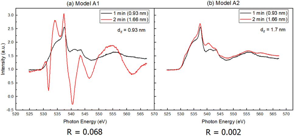
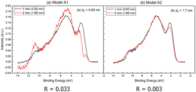
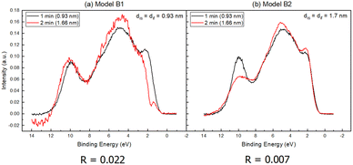
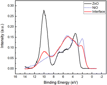
Fig. 5 shows that Model A2 has lower R factor than Model A1, suggesting that the interface states extend up to 1.7 nm toward the side of the interfacial layer, instead of merely 0.93 nm (Fig. 6 and 7). The average of the two curves of Model A2 is shown together with the UPS spectra of the ZnO substrate and thickest NiO film (Fig. 6). On the other hand, Fig. 8 shows that Model B2 has lower R factor than Model B1, suggesting that the interface states extend up to 1.7 nm on either side of the NiO–ZnO interface. The average of the two curves of Model B2 is shown together with the the UPS spectra of the ZnO substrate and thickest NiO film (Fig. 8). Between Models A2 and B2, however, Model A2 has the lower R factor, indicating that our model for UPS favors the assumption that interface states are present only on the side of the NiO film that extends up to 1.7 nm.
 |
| | Fig. 5 Two variants of Model A obtained using different dif values. (a) Model A1, where dif = 0.93 nm; (b) Model A2, where dif = 1.7 nm. Model A2 exhibits lower R factor, indicating higher similarity between the two variants. | |
 |
| | Fig. 6 Comparison of the spectra for the ZnO substrate, the thickest NiO film [both from Fig. 4(a)], and the interface electronic state from Model A2. | |
 |
| | Fig. 7 Two variants of Model B obtained using different dif and dis values. (a) Model B1, where dis = dif = 0.93 nm; (b) Model B2, where dis = dif = 1.7 nm. Model B2 exhibits lower R factor, indicating higher similarity between the two variants. | |
 |
| | Fig. 8 Comparison of the spectra for the ZnO substrate, the thickest NiO film [both from Fig. 4(a)], and the interface electronic state from Model B2. | |
X-ray absorption spectroscopy (XAS)
The experimental data in Fig. 9(a) were obtained from the report by Li et al.1 The experimental XAS spectrum of the 90 min NiO film is similar to the XAS spectra at O 1s threshold of NiO thin films in the study of Gutiérrez et al.,29 and is thus taken to be the bulk NiO spectrum, INiOO. Similarly, the experimental XAS spectrum of the ZnO (0001) substrate appears similar to that of bulk ZnO in the study of Dong et al.30 Hence, the ZnO spectrum is taken as the bulk ZnO spectrum, IZnOO. Fig. 9(b)–(d) were produced using the corresponding equations, i.e. (b) was obtained using eqn (1); (c) was obtained by subtracting (b) from (a); (d) was obtained using eqn (2). Similar to the UPS section, the troughs in the spectra ranging from 1 min to 10 min in Fig. 9(c) suggests the possible presence of interfacial electronic states at the valence band due to the discrepancy between experiment and model spectra.
 |
| | Fig. 9 (a) Experimental XAS spectra of NiO films of different thicknesses grown on ZnO (reproduced with permission from Li et al.1). (b) Model XAS spectra obtained via eqn (1). (c) Difference spectra obtained by subtracting the model spectra from the experimental spectra. (d) Sequential difference of each deposition interval obtained using eqn (2). | |
Likewise, we conduct error analysis via R factor to quantify the similarity between the interface signal when d = 0.93 nm and 1.66 nm.
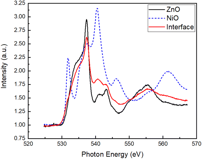
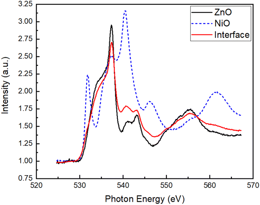
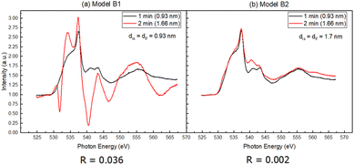
Fig. 10 shows that Model A2 has lower R factor than Model A1, suggesting that the interface states extend up to 1.7 nm toward the side of the interfacial layer (Fig. 11). The average of the two curves of Model A2 is shown together with the XAS spectra of the ZnO substrate and thickest NiO film (Fig. 11). On the other hand, Fig. 12 shows that Model B2 has lower R factor than Model B1, suggesting that the interface states extend up to 1.7 nm on either side of the NiO–ZnO interface (Fig. 13). The average of the two curves of Model B2 is shown together with the XAS spectra of the ZnO substrate and thickest NiO film (Fig. 13). For XAS, Models A2 and B2 exhibit similar R factor, but, since Model A2 for UPS exhibits the smallest R factor, Model A2 is chosen to be the most feasible model for the UPS and XAS modeling of the interfacial state spectra of a NiO–ZnO interface. This is corroborated by the fact that a 1.7 nm interfacial layer was observed in the report by Li et al.1 during film growth.
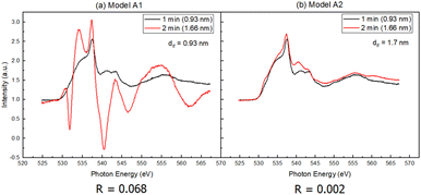 |
| | Fig. 10 Two variants of Model A obtained using different dif values. (a) Model A1, where dif = 0.93 nm; (b) Model A2, where dif = 1.7 nm. Model A2 exhibits lower R factor, indicating higher similarity between the two variants. | |
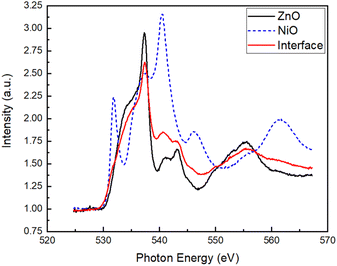 |
| | Fig. 11 Comparison of the spectra for the ZnO substrate, the thickest NiO film [both from Fig. 9(a)], and the interface electronic state from Model A2. | |
 |
| | Fig. 12 Two variants of Model B obtained using different dif and dis values. (a) Model B1, where dis = dif = 0.93 nm; (b) Model B2, where dis = dif = 1.7 nm. Model B2 exhibits lower R factor, indicating higher similarity between the two variants. | |
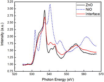 |
| | Fig. 13 Comparison of the spectra for the ZnO substrate, the thickest NiO film [both from Fig. 9(a)], and the interface electronic state from Model B2. | |
Conclusions
The interface electronic states of a NiO epitaxial thin film grown on ZnO were modeled based on existing UPS and XAS spectra of their respective bulk phases. Two models were proposed (Models A and B), one that accounts for only film contribution to the interface states (Model A), and another that accounts for both substrate and film contribution (Model B). Two variants for each model were constructed by varying the contributions of substrate and film accordingly, and similarity testing at 1 min and 2 min film growth was done for each model to test for model consistency and error margin using a reliability factor (R factor). It was observed that Model A2 exhibited the lowest R factor for both UPS and XAS, and that this occurred when it was assumed that only the NiO film contributed to the interface states that extended up to 1.7 nm, corroborated by the observation of an interfacial layer of similar thickness in the report by Li et al.1 Therefore, we conclude that Model A2 is the most reliable model when used to model the interfacial electronic states of an epitaxial thin film system. This work demonstrates the feasibility to extend the modelling methodology of interfacial electronic states previously proposed by Wang et al.20 for UPS spectra (probing the occupied states in the valence bands) to XAS spectra (probing the unoccupied states in the conduction bands). This approach of determining the interface structure model and the interfacial electronic states through UPS and/or XAS spectra may be extended to other types of interfaces as well, and may be considered as a preliminary step in any attempt to elucidate the interfacial electronic states of various other heterostructures.
Local symmetry has been identified as a significant factor in various phenomena, including thermoelectric transport various phenomena, e.g. thermoelectric transport,31 thermal rectification,32 and interfacial electronic states.33 Recent theoretical work has shown the presence of two interfaces driven by local symmetry in the (ZnO)n/(w-FeO)n superlattices.33 If such interesting local-symmetry-induced interfaces can be realized experimentally, the model proposed in this work will be well-suited for examining interface properties. With the advancement of characterization techniques,25,34–37 and the development of materials informatics and machine learning,38 the combination of our proposed model and big data in materials science may contribute to the in-depth study of interfaces.
Author contributions
Y. Y. Chan: data curation, formal analysis, investigation, writing – original draft. Z. C. Tey: data curation, formal analysis, investigation. H. Q. Wang: conceptualization, methodology, supervision, writing – review & editing.
Conflicts of interest
There are no conflicts to declare.
Acknowledgements
This research was supported by Xiamen University Malaysia Research Fund (Grant No: XMUMRF/2022-C9/IORI/0003).
Notes and references
- Y. Li, H.-Q. Wang, K. Ibrahim, J.-O. Wang, R. Wu, H.-J. Qian, H. Wang, T. Lei, Z. Wang, X. Li, M. Wu, J.-C. Zheng, J. Kang, L. Zhang, K. Kisslinger, L. Wu and Y. Zhu, Phys. Rev. Mater., 2020, 4, 124601 CrossRef CAS.
- H. Zheng, Y. Li, H. Liu, X. Yin and Y. Li, Chem. Soc. Rev., 2011, 40, 4506–4524 RSC.
- P.-C. Chen, M. Liu, J. S. Du, B. Meckes, S. Wang, H. Lin, V. P. Dravid, C. Wolverton and C. A. Mirkin, Science, 2019, 363, 959–964 CrossRef CAS PubMed.
- X. Du, Z. Mei, Z. Liu, Y. Guo, T. Zhang, Y. Hou, Z. Zhang, Q. Xue and A. Y. Kuznetsov, Adv. Mater., 2009, 21, 4625–4630 CrossRef CAS.
- S. Pearton and F. Ren, Curr. Opin. Chem. Eng., 2014, 3, 51–55 CrossRef.
- H. Long, S. Li, X. Mo, H. Wang, H. Huang, Z. Chen, Y. Liu and G. Fang, Appl. Phys. Lett., 2013, 103, 123504 CrossRef.
- N. Zhang, K. Yu, Q. Li, C. Song, L. Zhu and Z. Zhu, Mater. Lett., 2014, 121, 231–233 CrossRef CAS.
- Y.-L. Li, Z. Fan and J.-C. Zheng, J. Appl. Phys., 2013, 113, 083705 CrossRef.
- R. Wang and J.-C. Zheng, Phys. Chem. Chem. Phys., 2024, 26, 5848–5857 RSC.
- Y. Nakano, T. Morikawa, T. Ohwaki and Y. Taga, Appl. Phys. Lett., 2006, 88, 172103 CrossRef.
- D. C. Look, K. Leedy, L. Vines, B. Svensson, A. Zubiaga, F. Tuomisto, D. R. Doutt and L. Brillson, Phys. Rev. B: Condens. Matter Mater. Phys., 2011, 84, 115202 CrossRef.
- H. Ohta, M. Hirano, K. Nakahara, H. Maruta, T. Tanabe, M. Kamiya, T. Kamiya and H. Hosono, Appl. Phys. Lett., 2003, 83, 1029–1031 CrossRef CAS.
- Y. Vygranenko, K. Wang and A. Nathan, Appl. Phys. Lett., 2006, 89, 172105 CrossRef.
- Y. Xi, Y. Hsu, A. Djurišić, A. Ng, W. Chan, H. Tam and K. Cheah, Appl. Phys. Lett., 2008, 92, 113505 CrossRef.
- S.-Y. Tsai, M.-H. Hon and Y.-M. Lu, Solid-State Electron., 2011, 63, 37–41 CrossRef CAS.
- M. R. Hasan, T. Xie, S. C. Barron, G. Liu, N. V. Nguyen, A. Motayed, M. V. Rao and R. Debnath, APL Mater., 2015, 3, 106101 CrossRef PubMed.
- Z.-G. Yang, L.-P. Zhu, Y.-M. Guo, W. Tian, Z.-Z. Ye and B.-H. Zhao, Phys. Lett. A, 2011, 375, 1760–1763 CrossRef CAS.
- M. Ma, B. Lu, T. Zhou, Z. Ye, J. Lu and X. Pan, J. Appl. Phys., 2013, 113, 163704 CrossRef.
- T. A. Dar, A. Agrawal, P. Misra, L. M. Kukreja, P. K. Sen and P. Sen, Curr. Appl. Phys., 2014, 14, 171–175 CrossRef.
- H.-Q. Wang, E. I. Altman and V. E. Henrich, Phys. Rev. B: Condens. Matter Mater. Phys., 2008, 77, 085313 CrossRef.
- A. Nielsen, A. Brandlmaier, M. Althammer, W. Kaiser, M. Opel, J. Simon, W. Mader, S. T. Gönnenwein and R. Gross, Appl. Phys. Lett., 2008, 93, 162510 CrossRef.
- M. Paul, D. Kufer, A. Müller, S. Brück, E. Goering, M. Kamp, J. Verbeeck, H. Tian, G. Van Tendeloo, N. Ingle, M. Sing and R. Claessen, Appl. Phys. Lett., 2011, 98, 012512 CrossRef.
- A. Müller, A. Ruff, M. Paul, A. Wetscherek, G. Berner, U. Bauer, C. Praetorius, K. Fauth, M. Przybylski, M. Gorgoi, M. Sing and R. Claessen, Thin Solid Films, 2011, 520, 368–373 CrossRef.
- M. Paul, D. Kufer, A. Müller, A. Ruff, M. Kamp, N. Ingle, M. Sing and R. Claessen, J. Appl. Phys., 2011, 110, 073519 CrossRef.
- H.-Q. Wang, J. Xu, X. Lin, Y. Li, J. Kang and J.-C. Zheng, Light: Sci. Appl., 2021, 10, 153 CrossRef CAS PubMed.
- J. E. Whitten, Appl. Surf. Sci. Adv., 2023, 13, 100384 CrossRef.
- J. M. McKay and V. Henrich, Surf. Sci. Spectra, 1998, 5, 169–171 CrossRef CAS.
- E. I. Solomon and V. Henrich, Surf. Sci. Spectra, 1998, 5, 186–188 CrossRef CAS.
- A. Gutiérrez, G. Domínguez-Cañizares, S. Krause, D. Díaz-Fernández and L. Soriano, J. Vac. Sci. Technol., A, 2020, 38, 033209 CrossRef.
- C. Dong, C. Persson, L. Vayssieres, A. Augustsson, T. Schmitt, M. Mattesini, R. Ahuja, C. Chang and J.-H. Guo, Phys. Rev. B: Condens. Matter Mater. Phys., 2004, 70, 195325 CrossRef.
- J.-C. Zheng, Research, 2022, 2022, 9867639 CrossRef CAS.
- F.-Y. Du, W. Zhang, H.-Q. Wang and J.-C. Zheng, Chin. Phys. B, 2023, 32, 064402 CrossRef.
- J.-X. Gao, Y. S. Ng, H. Cheng, H. Wang, T.-Y. Lü and J.-C. Zheng, Phys. Chem. Chem. Phys., 2024, 26, 12084–12096 RSC.
- J.-C. Zheng, A. Frenkel, L. Wu, J. Hanson, W. Ku, E. Božin, S. Billinge and Y. Zhu, Phys. Rev. B: Condens. Matter Mater. Phys., 2010, 81, 144203 CrossRef.
- J.-C. Zheng, Y. Zhu, L. Wu and J. W. Davenport, J. Appl. Crystallogr., 2005, 38, 648–656 CrossRef CAS.
- J.-C. Zheng, L. Wu and Y. Zhu, J. Appl. Crystallogr., 2009, 42, 1043–1053 CrossRef CAS.
- J. Zheng and H. Wang, Sci. Sin.: Phys. Mech. Astron., 2021, 51, 030007 Search PubMed.
- S. S. Chong, Y. S. Ng, H.-Q. Wang and J.-C. Zheng, Front. Phys., 2024, 19, 13501 CrossRef.
|
| This journal is © The Royal Society of Chemistry 2024 |
Click here to see how this site uses Cookies. View our privacy policy here. 
 Open Access Article
 This Open Access Article is licensed under a Creative Commons Attribution-Non Commercial 3.0 Unported Licence
 *ab
*ab