
 Open Access Article
 This Open Access Article is licensed under a Creative Commons Attribution-Non Commercial 3.0 Unported Licence
Highly improved photocurrent of a flexible MoS2 photodetector via a backside Al metal mirror and its in- and outward folding states†
Hyewon Yoona and
Seongin Hong *ab
*ab
aDepartment of Physics, Gachon University, Seongnam 13120, Republic of Korea. E-mail: Seongin@gachon.ac.kr
bDepartment of Semiconductor Engineering, Gachon University, Seongnam 13120, Republic of Korea
First published on 4th November 2024
Abstract
High-performance foldable and flexible photodetectors have been extensively studied for next-generation hinged electronics and AR/VR technology. The need to maintain efficiency in the folded state restricts the development of strategies aimed at further improving the efficiency of photodetectors. For the first time, we introduce a simple and effective method for the photocurrent improvement of a molybdenum disulfide (MoS2) flexible photodetector by attaching a backside Al metal mirror and folding it in- and outward. Under light illumination, the Al film underneath the MoS2 photodetector acts as a flat reflective metal mirror and further functions as a concave mirror under the inward folded state. In this state, the proposed device with the backside Al metal mirror improved photocurrent from 4.04 μA to 8.53 μA under illumination (a λex of 405 nm with a Pinc of 0.3 mW cm−2) compared to the device on a flat polyimide (PI) substrate without the Al metal mirror. Our work provides new insights into high-performance flexible photodetectors in the inward and outward folded states, which will be beneficial for future foldable/hinged electronics and AR/VR devices.
Introduction
Recently, flexible technologies have been successfully applied to electronic devices such as smartphones.1–5 Notably, the Samsung Galaxy Z flip series is one of the most commercially successful foldable smartphones owing to its compact form factor when folded.6 However, most components such as sensors, batteries, antennas, and application processors (APs) in current foldable electronics are not yet actually flexible, except for displays.7,8 Among them, flexible photodetectors are in high demand for next-generation foldable/hinged electronics and AR/VR technology because they can provide the basis for flexible/foldable interactive display technology.9,10 Nevertheless, to date, few reports have attempted to improve the performance of photodetectors in the folded state owing to the need to maintain performance stability in the folded state. Meanwhile, two-dimensional (2D) transition metal dichalcogenides (TMDs) are considered promising candidates for next-generation semiconductors in flexible electronic devices because of their superior flexibility, high carrier mobility, and excellent transparency.11–19In this study, we developed a molybdenum disulfide (MoS2)-based flexible photodetector with a backside Al metal mirror, enabling enhanced photocurrent under in- and out-folded states. The device was systematically investigated under the polyimide (PI) substrate-only, backside Al metal mirror attached, outwardly folded, and inwardly folded states for performance comparison. Incremental changes in substrate conditions underneath the MoS2 photodetector resulted in gradual photocurrent improvement. In an inwardly folded state compared to the PI substrate-only state, the flexible MoS2 photodetector with a backside Al metal mirror improved photocurrent from 4.04 μA to 8.53 μA under illumination at a λex of 405 nm with a Pinc of 0.3 mW cm−2, which is attributed to function of the Al metal film as a concave mirror. The proposed photodetector configuration provides a route to photocurrent improvement under a folded state for future foldable electronics and AR/VR devices.
Experimental
Device fabrication
PI solution was spin-coated on an SiO2 (100 nm)/Si substrate at 500 rpm for 6 s and 1500 rpm for 60 s. PI on the SiO2/Si substrate was soft baked on a hot plate at 180 °C for 10 min and solidified in a siliconit furnace (DSF-232, Dae Heung science) at 350 °C for 2 h 30 min. The MoS2 flakes were mechanically exfoliated from bulk MoS2 crystal by standard scotch tape method and transferred onto the PI substrate. Standard photolithography process with lift-off technique was used to pattern the contact electrodes. Ag/Au (36/30 nm) was then deposited by a thermal evaporator at the rate of 1.0 Å s−1, and the non-patterned portions were lifted off in acetone. The PI substrate containing the MoS2 photodetectors was carefully peeled off from the rigid SiO2/Si substrate. Finally, one side sticky polyethylene terephthalate (PET) film was attached to the back of the PI substrate after Al was deposited on the PET film using the thermal evaporator.Characterization
The electric and optical properties of the flexible MoS2 photosensor were measured using a semiconductor device parameter analyzer (Keysight B1500A) and a multi-channel fiber-coupled laser source (Thorlabs MCLS1) at room temperature.Results and discussion
Fig. 1 shows the fabrication procedure of the MoS2-based flexible photodetectors on a PI substrate with a backside Al metal mirror. First, rigid SiO2/Si substrate was cleaned via ultra-sonication sequentially in acetone, isopropyl alcohol, and deionized water baths for 10 min each and then gently dried with a nitrogen gun. Solution polyimide (PI) was spin-coated onto the pre-cleaned rigid substrate at 500 rpm for 6 s and 1500 rpm for 60 s and soft baked at 180 °C for 10 min to eliminate the solvent, followed by curing in a siliconit furnace at 350 °C for 2 h 30 min. MoS2 flakes were exfoliated from bulk MoS2 crystals and transferred on the surface of the cured PI film/SiO2/Si substrate using the standard Scotch tape method. As shown in Fig. S1,† the Raman and PL spectra of bulk MoS2 flakes were obtained. The Raman peaks of the exfoliated bulk MoS2 flakes were obtained at 376 cm−1 (E12g) and 402 cm−1 (A1g). In the PL spectra, bulk MoS2 flakes show an invisible PL peak due to their indirect band gap. For the contact electrodes, Ag/Au (36/30 nm) was deposited and patterned using a thermal evaporator and conventional photolithography with lift-off technique, respectively. After carefully detaching the PI film from the SiO2/Si substrate, the flexible photodetectors based on MoS2 were successfully fabricated on the PI substrate. Finally, a PET film with pre-deposited Al (150 nm) was attached to the backside of the PI film, resulting in the proposed MoS2-based flexible photodetector with backside Al metal mirror. | ||
| Fig. 1 Schematic fabrication process flow of the MoS2-based flexible photodetector on a PI substrate with a backside Al metal mirror. | ||
Fig. 2a shows the actual photographs of the flexible MoS2 photodetectors before and after attaching Al metal-deposited PET film to the backside of the PI substrate. Since the PET film is a single-side adhesive, it could be easily attached to the back of the PI substrate after depositing Al on the non-adhesive surface of PET. Fig. 2b shows the optical microscopy image of the fabricated MoS2 photodetector on a PI substrate attached to an Al metal mirror, demonstrating that the MoS2 channel was placed between two Ag/Au electrodes. In order to investigate the photoresponsive characteristics of the flexible MoS2 photodetector on PI substrate, we measured the I–V curves of the device under illumination at an excitation wavelength (λex) of 406 nm with an incident power density (Pinc) of 0.3 and 0.6 mW cm−2, as shown in Fig. 2c. The MoS2 photodetector on the PI substrate exhibits a light on/off current ratio of over 2000 times. Fig. 2d shows the I–V characteristics of the device remeasured in the same way as that in Fig. 2c after attaching the Al metal mirror to the back of the PI substrate, indicating that the flexible MoS2 photodetector maintains excellent performance even after post-processing on the rear surface. Compared with the photocurrent (Iph = Itotal − Idark) of the flexible MoS2 photodetector before and after attaching the Al metal mirror, as shown in Fig. 2e and f, the photocurrent of the device after attaching the Al metal mirror became more significant as a function of applied voltage. Fig. 2g shows that the maximum photocurrent values extracted from the applied voltage of 10 V show the degree of improvement in the device after attaching the Al mirror. This photocurrent improvement is attributed to the Al metal film acting as a reflection metal mirror.
 | ||
| Fig. 2 Photoresponse characteristics of the MoS2-based flexible photodetector before and after attaching an Al metal mirror to the backside of the PI substrate. (a) Photograph of MoS2 photodetectors on a PI substrate only and the device with a backside Al metal mirror. The scale bar is 5 mm. (b) Optical microscopy image of the proposed MoS2 photodetector on a PI substrate with a backside Al metal mirror. Current–voltage (I–V) curves of (c) MoS2 photodetectors on a PI substrate and (d) the device with a backside Al metal mirror under dark conditions and illumination (λex of 406 nm and Pinc of 0.3 and 0.6 mW cm−2). (e) Extracted photocurrent as a function of applied voltage of the MoS2-based flexible photodetector on a PI substrate and (f) after attaching a Al metal mirror. (g) Comparison of maximum photocurrent as a function of the Pinc of the device before and after attaching a Al metal mirror. | ||
In order to further expand the role of the Al metal mirror underneath the MoS2 photodetector, we folded the device inward and outward using a plastic support, as shown in Fig. 3a and d, respectively. The measurement results in Fig. 3b and e show excellent photoresponse, which were under the same measurement conditions as that in Fig. 2d, except for the in- and out-folded states of the device. As a consequence, higher photocurrent is attained under illumination, as shown in Fig. 3c (out-folding state) and 3f (in-folding state) than in Fig. 2e (only PI substrate) and 2f (backside Al metal mirror). Such incremental changes in the substrate state result in a gradual increase in the photocurrent of the flexible MoS2 photodetector.
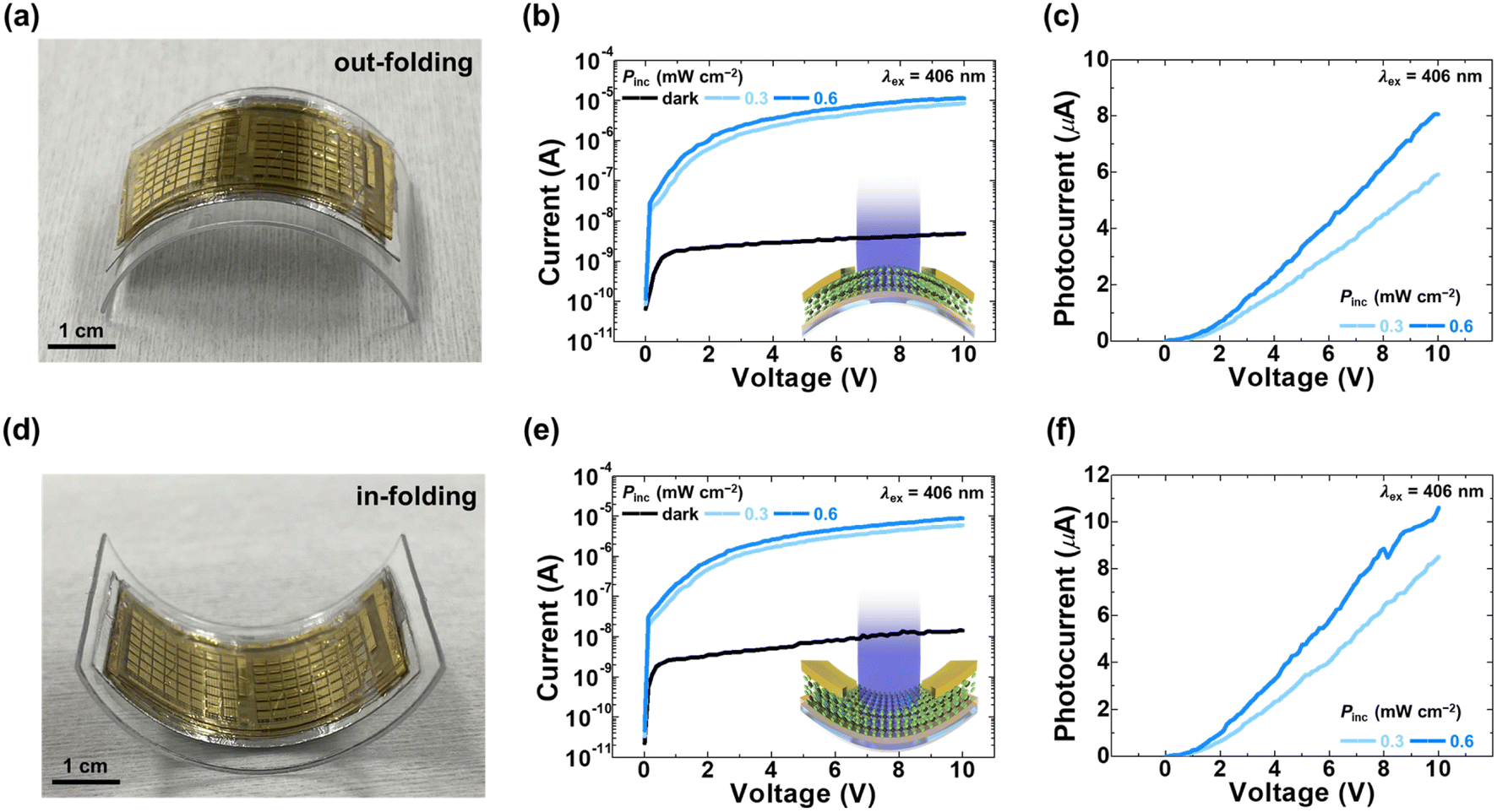 | ||
| Fig. 3 Photoresponse characteristics of the in- and out-folded modes of the backside Al metal mirror-integrated flexible photodetector. Digital pictures of the devices under the (a) in-folded and (d) out-folded states through a plastic support. The folding radius is 1.25 cm. I–V characteristics of the photodetector (b) folded inward and (e) folded outward under dark and illumination conditions (λex of 406 nm and Pinc of 0.3 and 0.6 mW cm−2). Photocurrent–voltage properties of the device in the (c) in-folded and (f) out-folded states. | ||
Fig. 4a shows the comparisons of the maximum photocurrent (Iph,max) of the device under substrate conditions: (1) PI substrate, (2) PI substrate with backside Al metal mirror, (3) folding the device outward, and (4) folding the device inward. As a result, the flexible MoS2 photodetector with a backside Al metal mirror under the in-folded state achieved the highest photocurrent among all the substrate conditions. Table 1 presents the Iph,max of the flexible MoS2 photodetector depending on the substrate state. The photocurrent gradually improves from (1) PI to (4) for the in-folded state. The maximum photocurrent value of the device for the in-folded state represents 8.5 μA and 10 μA (Pinc = 0.3 and 0.6 mW cm−2), respectively. It is ascribed to the Al metal film acting similar to a concave mirror underneath the MoS2 photodetector, as shown in Fig. 4b. Fig. S2† shows the photographs of the in- and out-folded state of the Al metal mirror without a photodetector. Comparison of the photo-switching characteristics of the MoS2 photodetector on the PI substrate and the in-folded substrate after attaching the backside Al metal mirror is shown in Fig. 4c. The current improvement of the MoS2 photodetector is evident on folding the substrate inward after attaching the Al metal mirror. Furthermore, the time-dependent photoresponse of the device under the in-folded state at various wavelengths is displayed in Fig. 4d, indicating the great periodical on/off light detection performance. To test the mechanical stability of the device, two sets of I–V characteristics of the MoS2 photodetector were measured: (1) photoresponsive characteristics with increasing folding diameter and (2) electrical characteristics in the flat state after folding with various folding diameters, as shown in Fig. S3.†
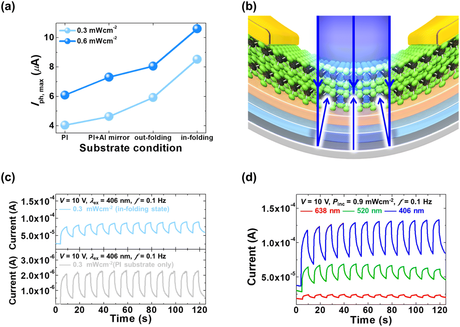 | ||
| Fig. 4 Photo-sensing performance of MoS2 photodetectors with a backside Al metal mirror in the in-folded state. (a) Comparison of the maximum photocurrent of the device under substrate conditions (PI only, PI with a backside Al metal mirror, out-folded, and in-folded state). (b) Schematic of the flexible device in the in-folded state, showing the role of a backside Al film as the concave metal mirror under illumination. (c) Comparison of the photo-switching properties of the flexible device on a PI substrate (bottom) and the in-folded state after attaching a backside Al metal mirror (top) under illumination (λex of 406 nm at Pinc of 0.3 mW cm−2, and f = 0.1 Hz). (d) Photo-switching properties of the flexible device folded inward under illumination by various wavelengths (λex of 638, 520, and 406 nm at Pinc 0.9 mW cm−2, and f = 0.1 Hz). | ||
| Photocurrent | Substrate condition | |||
|---|---|---|---|---|
| PI | PI + Al | Out-folded | In-folded | |
| Iph,max at Pinc = 0.3 μW cm−2 | 4.0 μA | 4.6 μA | 5.9 μA | 8.5 μA |
| Iph,max at Pinc = 0.6 μW cm−2 | 6.0 μA | 7.7 μA | 8.0 μA | 10 μA |
The charge transfer mechanism of the MoS2 flexible photodetector with Al metal mirror can be explained by the energy band diagram along the horizontal axis, as shown in Fig. 5. In Fig. 5a, the flat band state occurs when Vd is zero. The bulk MoS2 has an energy bandgap of 1.2 eV and its work function is 4.0 eV. The work function of Ag is 4.25 eV and that of Au is 5.1 eV. When positive Vd is applied, the energy band diagram is altered from Fig. 5a to b and electrons drift to drain by the electric field. Fig. 5c represents the generation of electron–hole pairs under UV light illumination in the MoS2 channel. As shown in Fig. 5d, since the illuminated light on the MoS2 channel was reflected by the Al metal mirror attached underneath the photodetector in the flat state, an increase in the electron–hole pairs was observed (Fig. 2g). Finally, we compared the charge transfer in two types of folding states: out-folded state (Fig. 5e) and in-folded state (Fig. 5f). Since the out-folded and in-folded state acted as convex and concave mirror, respectively, the light was more reflected than that in the flat state. Although the photocurrent improved for both the folding states, since the in-folded state facilitated the concentration of the reflected light in the MoS2 channel, the photocurrent showed the greatest improvement, as shown in Fig. 4a.
 | ||
| Fig. 5 Operating mechanism of the flexible MoS2 photodetector with a backside Al metal mirror. Energy band diagram of the MoS2 photodetector under (a) equilibrium, (b) on applying positive drain voltage, (c) on applying positive drain voltage with illumination, (d) on applying positive drain voltage with illumination and in the flat state, (e) on applying positive drain voltage with illumination and in the out-folded state, and (f) on applying positive drain voltage with illumination and in the in-folded state. | ||
Conclusions
We propose a simple and effective method for photocurrent improvement of a flexible MoS2 photodetector by attaching a backside Al metal film and folding it outward or inward. The backside Al film acts as a reflective metal mirror underneath the MoS2 channel, allowing us to obtain much higher photocurrent of the device. Furthermore, it can achieve a gradual increase in the photocurrent of the flexible MoS2 photodetector through incremental changes by folding the device outward or inward. Therefore, the flexible MoS2 photodetector with a backside Al metal mirror that can be used by folding outward and inward provides a promising strategy for high-performance flexible photo-sensing applications for future foldable electronics and AR/VR devices.Data availability
The data supporting this article have been included within the manuscript and its ESI.†Conflicts of interest
There are no conflicts to declare.Acknowledgements
This work was supported by the National Research Foundation of Korea (NRF) grant funded by the Korea government (MSIT) (No. RS-2023-0024456 and No. RS-2024-00445819).References
- W. Gao, S. Emaminejad, H. Y. Y. Nyein, S. Challa, K. Chen, A. Peck, H. M. Fahad, H. Ota, H. Shiraki and D. Kiriya, Nature, 2016, 529, 509–514 CrossRef PubMed.
- H. C. Ko, M. P. Stoykovich, J. Song, V. Malyarchuk, W. M. Choi, C.-J. Yu, J. B. Geddes Iii, J. Xiao, S. Wang and Y. Huang, Nature, 2008, 454, 748–753 CrossRef PubMed.
- X. Liu, D. Liu, J.-h. Lee, Q. Zheng, X. Du, X. Zhang, H. Xu, Z. Wang, Y. Wu and X. Shen, ACS Appl. Mater. Interfaces, 2018, 11, 2282–2294 CrossRef PubMed.
- Q. Pang, D. Lou, S. Li, G. Wang, B. Qiao, S. Dong, L. Ma, C. Gao and Z. Wu, Adv. Sci., 2020, 7, 1902673 CrossRef PubMed.
- S. Shi, Z. Li, L. Shen, X. Yin, Y. Liu, G. Chang, J. Wang, S. Xu, J. Zhang and Y. Zhao, Energy Storage Mater., 2020, 29, 78–83 CrossRef.
- J. Y. Yan, J. C. Ho and J. Chen, Inf. Disp., 2015, 31, 12–16 Search PubMed.
- X. Liao, C. Shi, T. Wang, B. Qie, Y. Chen, P. Yang, Q. Cheng, H. Zhai, M. Chen and X. Wang, Adv. Energy Mater., 2019, 9, 1802998 CrossRef.
- H.-J. Kwon, H. Shim, S. Kim, W. Choi, Y. Chun, I. Kee and S. Lee, Appl. Phys. Lett., 2011, 98, 151904 CrossRef.
- C. An, F. Nie, R. Zhang, X. Ma, D. Wu, Y. Sun, X. Hu, D. Sun, L. Pan and J. Liu, Adv. Funct. Mater., 2021, 31, 2100136 CrossRef CAS.
- W. Wu, X. Wang, X. Han, Z. Yang, G. Gao, Y. Zhang, J. Hu, Y. Tan, A. Pan and C. Pan, Adv. Mater., 2019, 31, 1805913 CrossRef PubMed.
- H. Cho, M. Sritharan, Y. Ju, P. Pujar, R. Dutta, W.-S. Jang, Y.-M. Kim, S. Hong, Y. Yoon and S. Kim, ACS Nano, 2023, 11279–11289 CrossRef CAS PubMed.
- A. Daus, S. Vaziri, V. Chen, Ç. Köroğlu, R. W. Grady, C. S. Bailey, H. R. Lee, K. Schauble, K. Brenner and E. Pop, Nat. Electron., 2021, 4, 495–501 CrossRef CAS.
- S. Hong, S. H. Choi, J. Park, H. Yoo, J. Y. Oh, E. Hwang, D. H. Yoon and S. Kim, ACS Nano, 2020, 14, 9796–9806 CrossRef CAS PubMed.
- S. Hong, N. Zagni, S. Choo, N. Liu, S. Baek, A. Bala, H. Yoo, B. H. Kang, H. J. Kim and H. J. Yun, Nat. Commun., 2021, 12, 3559 CrossRef CAS PubMed.
- K. Nassiri Nazif, A. Daus, J. Hong, N. Lee, S. Vaziri, A. Kumar, F. Nitta, M. E. Chen, S. Kananian and R. Islam, Nat. Commun., 2021, 12, 7034 CrossRef CAS PubMed.
- H. Park, D. S. Oh, K. J. Lee, D. Y. Jung, S. Lee, S. Yoo and S.-Y. Choi, ACS Appl. Mater. Interfaces, 2020, 12, 4749–4754 CrossRef CAS PubMed.
- E. Singh, P. Singh, K. S. Kim, G. Y. Yeom and H. S. Nalwa, ACS Appl. Mater. Interfaces, 2019, 11, 11061–11105 CrossRef CAS PubMed.
- R. Wu, Q. Tao, J. Li, W. Li, Y. Chen, Z. Lu, Z. Shu, B. Zhao, H. Ma and Z. Zhang, Nat. Electron., 2022, 5, 497–504 CrossRef CAS.
- S. Hong, J. Park, J. J. Lee, S. Lee, K. Yun, H. Yoo and S. Kim, NPG Asia Mater., 2021, 13, 38 CrossRef CAS.
Footnote |
| † Electronic supplementary information (ESI) available. See DOI: https://doi.org/10.1039/d4ra00459k |
| This journal is © The Royal Society of Chemistry 2024 |