 Open Access Article
Enhanced acetone gas-sensing characteristics of Pd–NiO nanorods/SnO2 nanowires sensors†
Nguyen Phu Hungab,
Nguyen Van Duyab,
Chu Thi Xuanab,
Dang Thi Thanh Le ab,
Chu Manh Hung
 ab,
Han Jinc and
Nguyen Duc Hoa
 *ab
*ab
aInternational Training Institute for Materials Science, Hanoi University of Science and Technology, No 1 Dai Co Viet, Hanoi, Vietnam. E-mail: hoa.nguyenduc@hust.edu.vn; ndhoa@itims.edu.vn
bSchool of Materials Science and Engineering, Hanoi University of Science and Technology, No 1 Dai Co Viet, Hanoi, Vietnam
cInstitute of Micro-Nano Science and Technology, School of Electronic Information and Electrical Engineering, Shanghai Jiao Tong University, Shanghai 200240, China
First published on 17th April 2024
Abstract
Acetone is a well-known volatile organic compound that is widely used in different industrial and domestic areas, but it can cause dangerous effects on human health. Thus, the fabrication of highly sensitive and selective sensors for recognition of acetone is incredibly important. Here, we prepared the SnO2/Pd–NiO (SPN) nanowires-based gas sensor for the detection of acetone, in which, the amount of Pd nanoparticles were varied to enhance the performance of the devices. We demonstrated that the acetone gas sensing performance of the SPN device was significantly enhanced, showing increases of 3.72 and 6.53 folds compared to pristine SnO2 and NiO sensors, respectively. The Pd–NiO 0.01% wt Pd SPN sensor (SPN-1) exhibited an excellent response (Ra/Rg = 14.88) toward 500 ppm acetone gas. The SPN-1 sensor also showed a fast gas response time of 11/150 seconds with 500 ppm Acetone at 450 °C, while the recovery time was 468/526 seconds. Additionally, the sensor showed good selectivity toward acetone over other reducing gases, such as NH3, CH4, and VOCs. With those results, the SPN-1 sensor shows superiority compared to sensors based on pure materials.
1. Introduction
Acetone, a colorless, highly volatile organic compound (VOC), is commonly found in industrial processes, laboratories, and medical facilities. However, this gas can have dangerous effects on human health when inhaled.1,2 Acetone concentrations higher than 173 ppm can severely affect the central nervous system and damage vital organs in the body. Furthermore, acetone can be biomarker in exhaled breath in disease diagnose, thus, its detection is significant due to its varied applications.2,3Concentrations of VOCs can be measured using standardized methods such as gas chromatography mass spectrometry, high-performance liquid chromatography, and proton transfer reaction mass spectrometry.4 These techniques have high sensitivity and precision for detection of various VOCs.1,4 Nevertheless, they are bulky, complex, expensive, time consuming, and need skilled operators for monitoring gases. Therefore, there is a need for small, portable, and fast dynamic devices that can easily detect acetone vapor.2
Devices designed specifically for acetone detection utilize diverse technologies such as chemoresistive sensors, electrochemical sensors, and optical sensors.5 These sensors function by detecting changes in electrical conductivity, chemical reactions, or light absorption when exposed to acetone molecules. The ability to monitor acetone levels is particularly valuable in medical diagnostics, where elevated acetone levels in breath can indicate conditions such as diabetes, making acetone gas sensors an essential tool in non-invasive disease detection.5–7 Furthermore, in industrial processes, these sensors contribute to ensuring workplace safety by monitoring acetone concentrations to prevent potential hazards associated with its exposure.8 So far, gas sensors based on n-type and p-type metal oxide semiconductors have attracted extensive attention owing to their simple operation, low power consumption, low cost, high sensitivity, and wide applicability in the real time monitoring of toxic and/or flammable gases.5,9
For n-type semiconductors, SnO2 nanowires are currently the most widely used material for detecting of various gases thanks to its advanced characteristics and low cost.9 SnO2 can sense to many gases or vapors at moderate temperatures10–19 because it has a high reactivity caused by the natural non-stoichiometry.10,11,14 Surface chemical reactions determine the gas-sensing properties; hence, an increasing number of studies focus on surface decoration to boost sensor sensitivity.18
For p-type semiconductor, nickel oxide (NiO) with a wide energy band gap of about the 3.6–4 eV is widely used in gas sensors.2,11,20 It demonstrates potential for use in gas sensors with good repeatability, high sensitivity, low cost, and environmentally friendly operation.20 It could serve as an important gas sensing material for acetone gas detection.2
Recently, nanostructured materials like nanowires, nanorods, and nanosheets were reported to have a high gas sensor response due to their ultrahigh surface-to-volume ratio.21 In addition, the presence of noble metal or metal oxide on the sensing material surface would improve its sensing properties due to the synergetic effect of catalyst and heterojunction.14,22 Noble metals lower activation energies, enhancing catalytic activity, generating active surface sites for increased oxygen adsorption, and reducing the operating temperature of the sensor.23 The significant improvement in gas sensing performance after noble metal decoration is due to two main mechanisms, namely (i) electronic sensitization, and (ii) chemical sensitization.14,22,24,25 Electronic sensitization is determined by the formation of the Schottky barrier between noble metal and semiconductor metal oxide. The Schottky barrier inhibit the recombination of electron–hole pairs and cause a significant change in resistance upon contact with the target gases.26 The chemical sensitization bases on the catalytic activity of the noble metal, which facilitate the dissociation of oxygen molecules to produce more reactive chemisorbed oxygen ions, which then spill onto the surface of SMO to react with more target gas molecules, known as the spillover effect.22,25 An example of this is the Pt/TiO2 sensor, which demonstrated exceptional detection capability for acetone gas by yielding a response of 13.6 to 50 ppm at 280 °C, thus offering promising practical applicability for devices relying on semiconducting metal oxide materials.27
Recently, the use of heterojunction between two different semiconductors was reported to significantly enhance the gas sensing performance.28 The p–p heterojunction in CuO–Co3O4 composite nanofibers was reported to show high sensitivity to hydrogen sulfide,29 whereas the n–n heterojunction of CeO2–SnO2 nanoparticles enhance the response to hydrogen.30 The p–n heterojunction of p-type Co3O4 and n-type In2O3 was reported to enhance the formaldehyde gas sensing properties.31 The heterojunction between SnO2 nanowires and NiO nanowires was also used for H2S gas sensor,32 but such report did not in details the sensing performance. Furthermore, none of the studies report utilizing the synergic effect of heterojunction between p–n junction of SnO2 and NiO in combination with the catalytic activity of Pd decoration to enhance the gas sensing performance. For instance, Cai et al.33,34 prepared hollow Pd–NiO/SnO2 yolk–shell particles for a hydrogen gas sensor, utilizing the spillover effect.
Here, we prepare the SnO2/Pd–NiO based acetone gas sensor. The use of Pd–NiO nanorods to decorate the SnO2 nanowires for gas sensor utilize the synergic effects of p–n heterojunction between p-type NiO and the n-type SnO2; and the catalytic effect of Pd nanoparticles. Our results point out that the SnO2/Pd–NiO based sensor exhibits 3.72 and 6.53 times higher than pristine SnO2 and NiO under identical experimental conditions, respectively. The sensor also exhibited excellent selectivity over the contamination of ammonia, ethylene, triethylamine, ethanol, and hydrogen.
2. Experimental
2.1 Materials
In the experimental process, the analytical substances consisting of pure tin powder (99.99% Sn), nickel(II) nitrate (NiNO3·6H2O), sodium oxalate (Na2C2O4), palladium nanoparticles (Pd NPs) solution (0.01 M) and ethylene glycol (EG) were used as precursors. The experimental part is divided into the following steps: (i) the growth of SnO2 nanowires using chemical vapor deposition method; (ii) synthesis of NiO nanorods using hydrothermal method; (iii) NiO nanorods decorated Pd nanoparticles before drop-casting to obtain sensors based on SnO2/Pd–NiO materials, as shown in Fig. 1.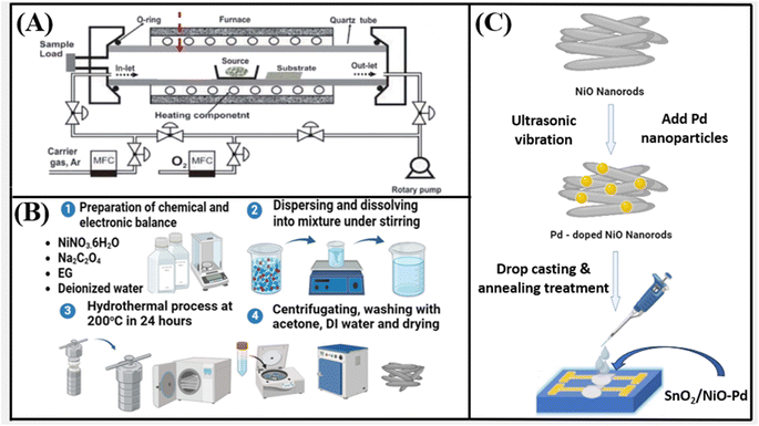 | ||
| Fig. 1 Schematic diagram of (A) the synthesis of SnO2 nanowires, (B) NiO nanorods, (C) and the gas sensor fabricated by the drop-casting process. | ||
2.2 Preparation of SnO2 nanowires
The SnO2 nanowire sensors were directly grown on thermally oxidized silicon substrate using chemical vapor deposition method (CVD).35 In a typical procedure, pure Sn powders were placed on a ceramic boat as an evaporation source. A thermally oxidized silicon substrate with Pt electrodes was also placed in the center of the boat. The next step is placing this quartz tube in the center of the horizontal furnace so that the boat containing the source powder is in the correct position in the center of the furnace as shown in Fig. 1A. The experimental process is divided into the following stages: (1) the quartz tube was evacuated to pressure of 10−2 Torr, and purged several times with high purity N2 gas with a flow rate of 300 sccm, then evacuated return to 10−2 Torr; (2) the furnace temperature was increased from room temperature to 750 °C for 20 min. It should be noted that the N2 gas flow was not introduced during this step; (3) soon after the furnace reached and stabilized at the synthesis temperature, oxygen gas (O2) was introduced into the quartz tube with a flow rate of 0.5 sccm and pressure inside the quartz tube is about 10−1 Torr. The growth process was maintained for 15 min; (4) after finishing the growth process of SnO2 nanowires the furnace was cooled down naturally to room temperature.13,15,18,362.3 Preparation of NiO nanorods
To synthesize NiO nanorods, we use the hydrothermal method in this process as shown in Fig. 1B.11 Briefly, 0.5 (g) NiNO3·6H2O and 0.29 (g) Na2C2O4 were dissolved in a mixed solution of 32 mL ethylene glycol and 18 mL deionized water to obtain a green solution. The solution was then transferred into a 100 mL-volume Teflon autoclave and the hydrothermal process took place at 200 °C for 24 h. After being cooled down naturally to room temperature, the precipitated Ni(OH)2 nanorods were collected and washed several times with deionized water and ethanol solvent to remove contaminated and unexpected ions. Finally, NiO nanorods were obtained by calcination at 500 °C for 2 h in air.11,162.4 Preparation of Pd–NiO nanorods and fabrication of SnO2/Pd–NiO gas sensors
The Pd–NiO nanorod materials were prepared by mixing NiO nanorods with Pd nanoparticles solution under ultrasonic vibration process, as shown in Fig. 1C. In this process, 10 (mg) of the collected NiO nanorods powders and different amount of Pd nanoparticles were dispersed in 3 μL N-vinylpyrrolidone (NVP) solvent for 20 minutes through an ultrasonic bath to form a colloidal solution. The NiO nanorods were mixed with Pd nanoparticles on various ratios (0.01 wt%, 0.02 wt%, and 0.04 wt%), respectively. The mass of Pd nanoparticles used in this process can be calculated through the precursor solutions used in previous reports of our group.37 The Pd–NiO nanorods colloidal solutions were then dropped on the surface of SnO2 nanowire devices to form SnO2/Pd–NiO sensors. The fabricated sensors were then annealed at 500 °C for 2 h to evaporate the solvent and to reduce the defects.The morphology, chemical composition, and structural characteristics of the pristine SnO2 nanowires and SnO2/Pd–NiO were investigated by Scanning Electron Microscopy (SEM; JEOL 7600F), Energy-Dispersive X-ray Spectroscopy (EDS), and X-ray Diffraction (XRD, D2 Phaser, Bruker) with Cu Kα radiation. The gas sensing properties of the fabricated sensors were studied by measuring the change in resistance upon exposure to different gases of various concentrations. Details about the gas sensing measurement system can be found in ref. 38. The response value of the sensor was determined by the ratio of Ra/Rg toward acetone gas, where Ra and Rg were the resistances of the sensor in air and target gas, respectively.
3. Results and discussion
3.1 Characterization of materials
To investigate the influence of the manufacturing process on the morphologies, crystal structures and gas sensing properties of SnO2/Pd–NiO materials, we carried out by using SEM, EDS-mapping, XRD, I–V and gas sensing properties for acetone gas.SEM images of the SnO2, NiO and SPN-1 materials are shown in Fig. 2. As shown in Fig. 2A(1)–(3), the SnO2 material synthesized by CVD method has the nanowire structures deposited on the Pt electrode. The length of the nanowires is a few micrometers. Such nanowires were grown on the surface of the Pt electrodes. In our separated study, the SnO2 nanowire is a single crystal, with an average diameter of about 80 nm (data not shown). The NiO material fabricated by hydrothermal method showed the morphology of nanorods, as shown in Fig. 2B(1)–(3). The length of the NiO nanorods was less than 5 micrometers. The diameters of the SnO2 nanowires and the NiO nanorods are estimated from the high magnification SEM images (Fig. S4, ESI†) to be about 80 nm and 100 nm, respectively. Meanwhile, SPN-1 material was a combination of two structural forms of these two materials, as shown in Fig. 2C(1)–(3). Here, due to the small size of Pd nanoparticles, they could not be visualized by SEM image. Anyhow, the three sensors show the existence of the nanomaterials deposited on the Pt interdigitated electrodes for electrical and gas sensing measurement.
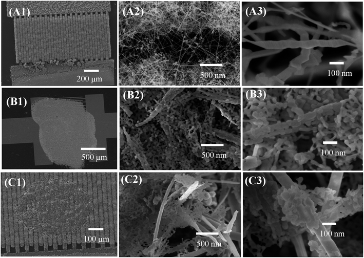 | ||
| Fig. 2 The SEM images of sensors with different magnifications: (A) SnO2 nanowires, (B) NiO nanorods, and (C) SPN-1 sensor. | ||
The SEM image could not show the evidence of the Pd nanoparticles on the sample due to the small size of Pd. However, we presented evidence to show the presence of Pd nanoparticles in the EDS-spectrum analysis section, Fig. 3. To evaluate the chemical composition of the SPN-1 material, EDS-mapping was conducted at 15 keV. Fig. 3A showed the dependence of the intensity of chemical elements on X-ray radiation energy. The EDS results showed that the sample had complete presence of necessary chemical elements such as Sn, Ni, O, and Pd with the mass percentage at 40.3 wt%, 26.18 wt%, 32.23 wt%, and 1.38 wt%, respectively. The obtained results demonstrated similarity with the theoretically predicted values, thereby providing partial affirmation of the successful fabrication of the SPN-1 material. In addition, elemental mappings were carried out to offer ESI† about the surface distribution of chemical elements, as depicted in Fig. 3B–F. The EDS mapping showed a relatively uniform distribution of chemical elements across the surface, with Sn, Ni, and O exhibiting a dense distribution. Notably, Pd nanoparticles showed a much lower density, corresponding to the lowest mass (atomic) percentage among the elements depicted in Fig. 3C–F. This result is completely consistent with the initial theoretical calculation.
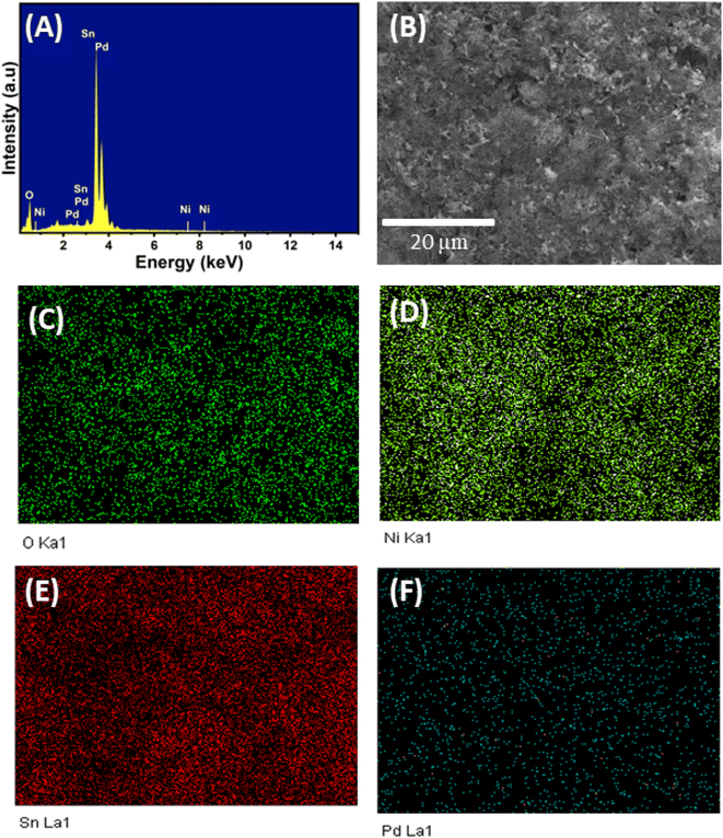 | ||
| Fig. 3 (A) The EDS spectrum of SPN-1 sensor, (B) the SEM image of SPN-1, the elemental mapping of (C) O, (D) Ni, (E) Sn, and (F) Pd, respectively. | ||
X-ray diffraction was used to study the crystal structure of the synthesized materials. Fig. 4 showed the X-ray diffraction patterns of pure SnO2 nanowires, NiO nanorods, and Pd–NiO decorated SnO2 nanowires with various mass ratios Pd/NiO (0.01, 0.02, and 0.04 wt%). The X-ray diffraction (XRD) peaks observed in the pure SnO2 and NiO materials align perfectly with the standard profiles of SnO2 featuring a Rutile structure (ICDD 41-1445) and NiO displaying a Rocksalt crystal structure (ICDD 04-0835). In contrast, the XRD patterns of the SnO2/Pd–NiO composite material samples exhibit an amalgamation of these two distinct structures. The introduction of Pd in the SnO2/Pd–NiO composites did not induce any discernible alterations in the crystal structures of the constituent materials. Notably, the XRD patterns do not reveal the diffraction peaks associated with Pd nanoparticles, probably attributed to their minimal presence in the composites. The attained materials exhibit distinctive diffraction peaks characteristic of both pure SnO2 and NiO, providing partial confirmation of the successful synthesis of SnO2/Pd–NiO composites. The intensity of the diffraction peaks undergoes variations based on the mass percentage relationship between Pd nanoparticles and NiO nanorods during the synthesis process. Specifically, an increase in the mass percentage of Pd-doped NiO leads to a reduction in the intensity of X-ray diffraction peaks in comparison to the pure SnO2 and NiO materials. This indicates the increased involvement of Pd nanoparticles and NiO nanorods in the final materials. Importantly, this outcome aligns perfectly with the initial project goal of combining three materials without altering the crystal structure of any constituent element.
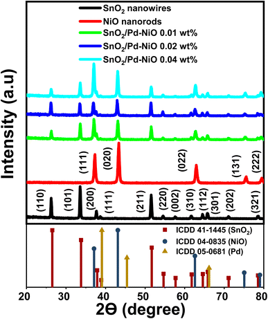 | ||
| Fig. 4 XRD patterns of the SnO2 nanowires, NiO nanorods, and SnO2/Pd–NiO with various contents Pd nanoparticles. | ||
3.2 Electrical and gas sensing properties
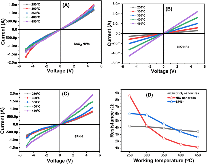
Prior to exploring the gas-sensitive properties, we conducted an analysis of the I–V characteristics of the fabricated sensors. This involved examining the electrical behavior of SnO2 nanowires, NiO nanorods, and SnO2/Pd–NiO nanowires sensors with varying mass ratios of Pd/NiO (0.01, 0.02, and 0.04 wt%) across the working temperature range (250–450 °C). Different bias voltages ranging from −5 V to 5 V were applied between the Pt electrodes during this investigation.The I–V plots of the SnO2 nanowires, NiO nanorods, and SnO2/Pd–NiO nanowires sensors are shown in Fig. 5A, B and C, respectively. The nonlinear dependence of the I–V plots found in the SnO2/Pd–NiO nanowires sensor (Fig. 5C) was possibly caused by the electron transfer of p–n structure between NiO and SnO2.39 This suggests the formation of ohmic contact between the Pt electrode and the sensing materials. In Fig. 5D, the base resistance of the sensors decreases as the temperature rises from 250 °C to 450 °C. This phenomenon can be attributed to the thermal excitation of electrons from valence band to conduction. This means in the working temperature range, the dominant factor influencing the conduction change is thermal excitation energy. The ohmic contact is important in understand the gas sensing mechanism because it ensures the change in sensor resistance upon exposure to analytic gas caused by the surface interaction between gas molecules and the sensing materials.40
In this investigation, three SnO2/Pd–NiO sensors, each featuring distinct ratios of noble metal Pd nanoparticles and NiO nanorods (0.01 wt%, 0.02 wt%, and 0.04 wt%), were examined for their ability to detect acetone gas within the concentration range of 25–500 ppm. Before introducing acetone gas into the measurement chamber, the baseline resistance was stabilized by aging in air for 2 h. Upon reaching a steady state, acetone gas with desired concentration was introduced into the chamber. During each cycle, the sensors were exposed to acetone gas for 100 seconds, followed by recovery to the baseline resistance through the introduction of airflow into the measuring chamber at a rate of 400 sccm. Investigation of different ratios of Pd–NiO nanorods dopant on the surface of SnO2 nanowires is crucial for determining the optimal sensor and investigating their gas sensing characteristics. Three distinct ratios (0.01 wt%, 0.02 wt%, and 0.04 wt%), namely SPN-1, SPN-2, and SPN-4, were studied and we found that the SPN-1 demonstrated a superior response toward acetone as compared with others (Fig. S1, ESI†).
As illustrated in Fig. 6A, the SPN-1 sensor was exposed to increasing concentrations of acetone gas at various working temperatures. Notably, the SPN-1 sensor exhibited an excellent response to 500 ppm acetone gas at high temperatures, demonstrating a fast response time of 11/150 seconds at 450 °C. The response time of the sensor increased with the decrease in introduced gas concentration. On the contrary, the recovery times of the sensor decreased when exposed to lower acetone concentration, with values maintained below 550 seconds. This phenomenon occurred due to the gas adsorption and desorption mechanism. The acetone gas molecules could easily react with the surface of sensing materials at high acetone gas concentration. However, the acetone gas molecules could be easily desorbed from the surface of sensing materials at low concentrations after introducing airflow into the measuring chamber. Additionally, Fig. 6B showed the dependence of sensor response on acetone concentration, in which the SPN-1 sensor exhibited a linear correlation between its response to acetone gas concentrations at various working temperatures. The highest response of the SPN-1 sensor reached 14.88 when exposed to 500 ppm of acetone gas at 450 °C.
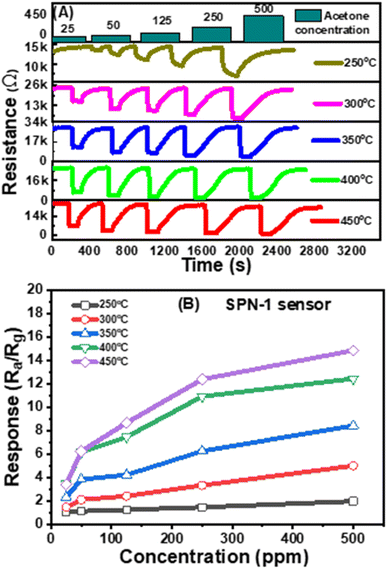 | ||
| Fig. 6 (A) The resistance of SPN-1 sensor at various working temperatures; (B) sensor response as a function of the acetone concentration. | ||
The SPN-1 sensor with lower Pd content exhibited higher sensitivity. Reducing the content of Pd in the sample may increase the sensitivity, but it is a challenge in effective decoration of Pd on the surface of NiO nanorods. Consequently, we proceed to utilize the SPN-1 sensor for the comparison of response with two sensors based on pristine SnO2 nanowires and NiO nanorods materials.
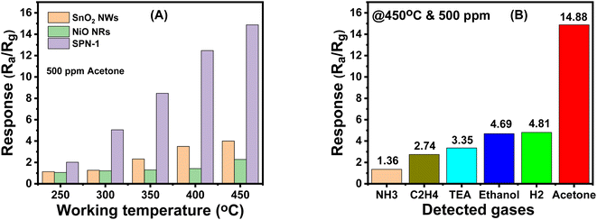
To demonstrate the response enhancement to acetone gas, pristine SnO2 nanowires, NiO nanorods, and SPN-1 sensors were exposed to concentration of 500 ppm acetone across a temperature spectrum ranging from 250 to 450 °C, as shown in Fig. 7. Fig. 7A illustrated a direct correlation between the sensors' responses and the operating temperatures, showing an upward trend with increased temperature. Although all sensors exhibited optimal performance at 450 °C, the SPN-1 sensor notably superior capability in detecting acetone gas. Specifically, the SPN-1 sensor highlighted a gas response 3.72 times higher than SnO2 and 6.53 times higher than NiO under identical experimental conditions.
Investigating the selectivity of the SPN-1 sensor across various gases was conducted at 450 °C. The sensor's performance was assessed while exposed to gases, namely NH3, C2H4, TEA (triethylamine), ethanol, and H2, each at a concentration of 500 ppm and a temperature of 450 °C. As depicted in Fig. 7B, the SPN-1 sensor exhibited detectability towards all gases. Specifically, the NH3 gas sensor exhibited the lowest response of 1.36, whereas the sensor's response to acetone was notably the highest, demonstrating a response of 14.88. As a result, the measured results demonstrated that the SPN-1 sensor showed an excellent selectivity toward acetone detection.
The short-term and long-term stability of the SPN-1 sensor was investigated to assess the stable response to acetone gas. For short-term stability assessment, a continuous sequence of 8 pulses with a concentration of 500 ppm acetone at 450 °C was conducted. The response of the sensor, shown in Fig. 8A, exhibited uniformity in most pulses. The sensor signal returned to the baseline resistance upon exposure to fresh air. Nevertheless, the overall response of the SPN-1 sensor remained stable throughout the duration of the experiment.
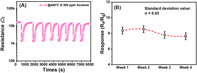 | ||
| Fig. 8 (A) The short-term stability and (B) long-term stability of the SPN-1 sensor after 4 weeks of testing with standard deviation. | ||
Regarding the assessment of long-term stability, the sensor was investigated in 4 continuous weeks. Notably, the sensor's response to acetone gas did not exhibit significant change over the duration of the long-term stability evaluation. The plot of sensor response with the standard deviation was presented in Fig. 8B. The observed standard deviation, which was lower than 1, signifies a diminished level of variability in the response values, indicating their proximity to the mean. Concurrently, the empirical measurements reveal a negligible reduction in response by 0.91 units over a testing period. This result underlines the stability and limited variance in the sensor's response characteristics during the extended testing duration.
We compare our results with others reports on acetone sensors. As summarized in Table 1, our sensor showed higher response as compared with the Co3O4 nanocubes, and the PANI/SnO2, but lower than others, regardless of working temperature. Despite that we demonstrated that the SnO2/Pd–NiO sensor significantly enhanced the response of 3.72 and 6.53 folds as compared to pristine SnO2 and NiO sensors, respectively. Optimization of the sensor structure and nanowire density can enhance the sensor response.
| Material | Method | Concentration | Response (Ra/Rg) | Temperature (°C) | Ref. |
|---|---|---|---|---|---|
| a Response defined as Ra/Rg.b Response defined as (Ra − Rg)/Ra × 100 (%). | |||||
| WO3 decorated with Au and Pd | Thermal evaporation | 1000 ppm | 6a | 300 | 41 |
| GO/BiFeO3 perovskite | Sol–gel | 500 ppm | 89b | 250 | 42 |
| Co3O4 nanocubes | Hydrothermal | 500 ppm | 4.88a | 240 | 43 |
| ZnO nanosheet | Hydrothermal | 50 ppm | 33a | 360 | 44 |
| Co3O4 nanosheet | Hydrothermal | 1000 ppm | 36.5a | 111 | 43 |
| PANI/SnO2 | Hydrothermal | 800 ppm | 1.68a | 60 | 45 |
| Rh doped SnO2 nanofibers | Electrospinning | 50 ppm | 60.6a | 200 | 46 |
| SnO2 nanosheet | Hydrothermal | 100 ppm | 9.8a | 310 | 47 |
| Pd–NiO nanorods/SnO2 nanowires | CVD, hydrothermal | 500 ppm | 14.88a | 450 | This work |
| O2 (gas) → O2 (ads) | (1) |
| O2 (ads) + e− → O2− (ads) | (2) |
| O2− (ads) + e− → 2O− (ads) | (3) |
| O− + e− → O2− (ads) | (4) |
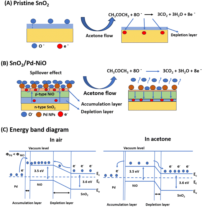
The adsorbed oxygen species captured electrons from SnO2 semiconductor and formed the electron depletion layer, Fig. 9A. Upon exposure to acetone, the reaction between adsorbed oxygen species and acetone molecule occurs following eqn (5)–(8)
| CH3COCH3 (gas) ↔ CH3COCH3 (ads) | (5) |
| 4O2− (ads) + CH3COCH3 (ads) → 3CO2 (gas) + 3H2O (gas) + 4e− | (6) |
| 8O− (ads) + CH3COCH3 (ads) → 3CO2 (gas) + 3H2O (gas) + 8e− | (7) |
| 8O2− (ads) + CH3COCH3 (ads) → 3CO2 (gas) + 3H2O (gas) + 16e− | (8) |
The reactions between adsorbed oxygen species and acetone molecule release electron back to SnO2 semiconductor and reduce the sensor resistance. Similar reactions also happened when NiO was exposed to air and acetone. However, the hole accumulation layer was formed and changed with test gases, thus resulting in increased sensor resistance upon exposure to acetone.51
According to the measured results, the SPN-1 sensor exhibited an improved gas sensing response compared to pure SnO2 and NiO sensors. The enhanced acetone sensing response can be attributed to two aspects (i) electronic sensitization, and (ii) chemical sensitization. The p–n heterojunction can be formed at the interface between p-type NiO and n-type SnO2. Due to the difference in electron and hole concentrations, electron (or hole) diffusion leads to the formation of a depletion region at the contact point between SnO2 and NiO.22,48 The enhancement of gas-sensing properties of SnO2/Pd–NiO was explained as the formation of p–n heterojunction, and expansion of the depletion region (Fig. 9B). Additionally, the catalytic properties of Pd nanoparticles are also crucial factors that enhance the response of the gas sensors due to the spillover effect.52,53 Due to the spillover effect occurred on the surface of Pd nanoparticles lead to the formation of more adsorbed oxygen species on the surface of SnO2/Pd–NiO sensing materials. After being exposed to acetone, the acetone molecules react with adsorbed oxygen species and release electrons back to the conduction bands, resulting in the decrease of depletion layer (Fig. 9B).14,22,49,50 As a result, the SnO2/Pd–NiO sensors exhibited an improved gas sensing property toward acetone. The energy band diagram of the SnO2/Pd–NiO sample is shown in Fig. 9(C).34 So, the contact between Pd and NiO formed the accumulation layer due to the work function of NiO is larger than that of Pd nanoparticles, so the electrons will transfer from the Pd nanoparticle into the conduction band of the NiO nanorods. However, the contact between n-type SnO2 and p-type NiO form the electron depletion layer. The electron depletion layer significantly changed with exposure to acetone, thus enhancing the sensor response.
4. Conclusion
In this study, we successfully synthesized SnO2 nanowires, NiO nanorods, and SnO2/Pd–NiO materials with various ratios content of Pd for Acetone gas sensors. The morphology, crystal structure, electrical and gas sensitive properties of the fabricated sensors were investigated. The SnO2/Pd–NiO materials with Pd content of 0.01 wt% (SPN-1) exhibited the best acetone sensing performance. The highest response of the SPN-1 sensor reached the value of 14.88 for 500 ppm acetone at 450 °C. The enhancement of acetone response was due to the catalytic properties of Pd nanoparticles, and the p–n heterojunction between SnO2 nanowires and NiO nanorods. The sensor also had fast response and recovery time of 11/150 seconds, while the recovery time was 468/526 seconds at 450 °C. The sensor exhibited a low detection limit of 25 ppm level. These results showed the potential of the sensor for applications in detecting harmful gases.Conflicts of interest
There are no conflicts to declare.Acknowledgements
This material is based upon work supported by the Air Force Office of Scientific under award number FA2386-22-1-4043; and the Vietnamese Ministry of Science and Technology in the Vietnam–Korea joint research program under grant number NĐT/KR/21/20.References
- T. Majchrzak, W. Wojnowski, M. Lubinska-Szczygeł, A. Różańska, J. Namieśnik and T. Dymerski, Anal. Chim. Acta, 2018, 1035, 1–13 CrossRef CAS PubMed.
- C. Li, P. G. Choi, K. Kim and Y. Masuda, Sens. Actuators, B, 2022, 367, 132143 CrossRef CAS.
- R. Epping and M. Koch, Molecules, 2023, 28(4), 1598 CrossRef CAS PubMed.
- Y. M. Lim, V. Swamy, N. Ramakrishnan, E. S. Chan and H. P. Kesuma, Microchem. J., 2023, 195, 109537 CrossRef CAS.
- Z. Yunusa, M. N. Hamidon, A. Kaiser and Z. Awang, Sens. Trans., 2014, 168(4), 61–75 Search PubMed.
- T. Kudo, Catal. Today, 1990, 8, 263–274 CrossRef CAS.
- M. I. A. Asri, M. N. Hasan, M. R. A. Fuaad, Y. M. Yunos and M. S. M. Ali, IEEE Sens. J., 2021, 21, 18381–18397 CAS.
- V. Ambardekar, T. Bhowmick, P. P. Bandyopadhyay and S. B. Majumder, J. Phys. Chem. Solids, 2022, 160, 110333 CrossRef CAS.
- L. Mahmood, M. Ghommem and Z. Bahroun, J. Appl. Comput. Mech., 2023, 9, 775–803 Search PubMed.
- Y. Zhu, H. Wang, J. Liu, M. Yin, L. Yu, J. Zhou, Y. Liu and F. Qiao, J. Alloys Compd., 2019, 782, 789–795 CrossRef CAS.
- C. Wei, B. Bo, F. Tao, Y. Lu, S. Peng, W. Song and Q. Zhou, J. Spectrosc., 2015, 2015, 450485 Search PubMed.
- T. T. Ngoc Hoa, N. D. Hoa, N. Van Duy, C. M. Hung, D. T. Thanh Le, N. Van Toan, N. H. Phuong and N. Van Hieu, RSC Adv., 2019, 9, 13887–13895 RSC.
- T. T. Ngoc Hoa, N. Van Duy, C. M. Hung, N. Van Hieu, H. H. Hau and N. D. Hoa, RSC Adv., 2020, 10, 17713–17723 RSC.
- C. Liu, Q. Kuang, Z. Xie and L. Zheng, CrystEngComm, 2015, 17, 6308–6313 RSC.
- Y. Lu, Y. Zhang, J. Liu, H. Li, Z. Hu, X. Luo, N. Gao, B. Zhang, J. Jiang, A. Zhong, J. Luo and H. Liu, Sens. Actuators, B, 2021, 345, 130334 CrossRef.
- D. Thi Thanh Le and C. Manh Hung, Commun. Phys., 2019, 29, 77 CrossRef.
- H. T. Nha, P. Van Tong, N. Van Duy, C. M. Hung and N. D. Hoa, J. Electron. Mater., 2021, 50, 2767–2778 CrossRef CAS.
- L. V. Thong, N. D. Hoa, D. T. T. Le, D. T. Viet, P. D. Tam, A. T. Le and N. Van Hieu, Sens. Actuators, B, 2010, 146, 361–367 CrossRef CAS.
- N. Van Toan, N. Viet Chien, N. Van Duy, H. Si Hong, H. Nguyen, N. Duc Hoa and N. Van Hieu, J. Hazard. Mater., 2016, 301, 433–442 CrossRef PubMed.
- N. D. Hoa and A. E. Sherif, Chem.–Eur. J., 2011, 17, 12896–12901 CrossRef CAS PubMed.
- J. Ding, Z. Zheng, Z. Song, S. Ding, J. Wen, K. Liu, C. Zhang and H. Li, Mater. Des., 2023, 234, 112360 CrossRef CAS.
- L. Y. Zhu, L. X. Ou, L. W. Mao, X. Y. Wu, Y. P. Liu and H. L. Lu, Advances in Noble Metal-Decorated Metal Oxide Nanomaterials for Chemiresistive Gas Sensors: Overview, Springer Nature Singapore, 2023, vol. 15 Search PubMed.
- V. T. Duoc, H. Nguyen, T. M. Ngoc, C. T. Xuan, C. M. Hung, N. V. Duy and N. D. Hoa, Int. J. Hydrogen Energy, 2024, 61, 774–782 CrossRef CAS.
- W. Weihua, T. Xuelin, C. Kai and C. Gengyu, Colloids Surf., A, 2006, 273, 35–42 CrossRef.
- J. Bai, C. C. Wang, K. Liu, H. Wang, Y. Liu, F. Liu, H. Suo, X. Liang, C. Zhang, F. Liu, C. Wang, P. Sun and G. Lu, Sens. Actuators, B, 2021, 330, 129375 CrossRef CAS.
- A. Kolmakov, D. O. Klenov, Y. Lilach, S. Stemmer and M. Moskovitst, Nano Lett., 2005, 5, 667–673 CrossRef CAS PubMed.
- M. Yan, X. Gao, X. Han, D. Zhou, Y. Lin, W. Chen, Z. Xue and Y. Wu, Small Struct., 2023, 4, 2200248 CrossRef CAS.
- L. Liu, Y. Wang, Y. Liu, S. Wang, T. Li, S. Feng, S. Qin and T. Zhang, Microsyst. Nanoeng., 2022, 8, 85 CrossRef CAS PubMed.
- P. H. Phuoc, N. N. Viet, N. V. Chien, N. Van Hoang, C. M. Hung, N. D. Hoa, N. Van Duy, H. S. Hong, D. D. Trung and N. Van Hieu, Sens. Actuators, B, 2023, 384, 133620 CrossRef CAS.
- D. E. Motaung, G. H. Mhlongo, P. R. Makgwane, B. P. Dhonge, F. R. Cummings, H. C. Swart and S. S. Ray, Sens. Actuators, B, 2018, 254, 984–995 CrossRef CAS.
- D. L. Kong, W. J. Wu, B. Hong, J. C. Xu, X. L. Peng, H. L. Ge, J. Li, Y. X. Zeng and X. Q. Wang, Ceram. Int., 2024, 50, 6995–7005 CrossRef CAS.
- D. Thi Thanh Le and C. Manh Hung, Commun. Phys., 2019, 29, 77 CrossRef.
- Y. Jung, J. Ahn, J. Kim, J. Ha, J. Shim, H. Cho, Y. S. Oh, Y. Yoon, Y. Nam, I. Oh, J. Jeong and I. Park, Small Methods, 2022, 32, 31–38 Search PubMed.
- H. Cai, N. Luo, X. Wang, M. Guo, X. Li, B. Lu, Z. Xue and J. Xu, Small, 2023, 19(42), 2302652 CrossRef CAS PubMed.
- T. M. Ngoc, N. Van Duy, N. Duc Hoa, C. Manh Hung, H. Nguyen and N. Van Hieu, Sens. Actuators, B, 2019, 295, 144–152 CrossRef CAS.
- C. M. Hung, D. T. T. Le and N. Van Hieu, J. Sci.: Adv. Mater. Devices, 2017, 2, 263–285 Search PubMed.
- T. T. Nguyet, D. T. Thanh Le, N. Van Duy, C. T. Xuan, S. Ingebrandt, X. T. Vu and N. D. Hoa, RSC Adv., 2023, 13, 13017–13029 RSC.
- N. Van Hieu, L. T. B. Thuy and N. D. Chien, Sens. Actuators, B, 2008, 129, 888–895 CrossRef CAS.
- G. Niu, C. Zhao, H. Gong, Z. Yang, X. Leng and F. Wang, Microsyst. Nanoeng., 2019, 5(21), 1–8 CAS.
- S. H. S. Pai, A. Mondal, R. Barathy T, B. Ajitha, J. J. Samuel E and Y. A. K. Reddy, Int. J. Hydrogen Energy, 2024, 50, 928–941 CrossRef CAS.
- S. Kim, S. Park, S. Park and C. Lee, Sens. Actuators, B, 2015, 209, 180–185 CrossRef CAS.
- P. Ghadage, K. P. Shinde, D. Nadargi, J. Nadargi, H. Shaikh, M. A. Alam, I. Mulla, M. S. Tamboli, J. S. Park and S. Suryavanshi, RSC Adv., 2024, 14, 1367–1376 RSC.
- V. Amiri, H. Roshan, A. Mirzaei, G. Neri and A. I. Ayesh, Sensors, 2020, 20(11), 1–25 CrossRef PubMed.
- H. Fan and X. Jia, Solid State Ionics, 2011, 192, 688–692 CrossRef CAS.
- L. Geng, Y. Zhao, X. Huang, S. Wang, S. Zhang and S. Wu, Sens. Actuators, B, 2014, 207(120), 568–572 Search PubMed.
- X. Kou, N. Xie, F. Chen, T. Wang, L. Guo, C. Wang, Q. Wang, J. Ma, Y. Sun, H. Zhang and G. Lu, Sens. Actuators, B, 2018, 256, 861–869 CrossRef CAS.
- H. Chen, Q. Wang, C. Kou, Y. Sui, Y. Zeng and F. Du, Sens. Actuators, B, 2014, 194, 447–453 CrossRef CAS.
- J. Hu, J. Yang, W. Wang, Y. Xue, Y. Sun, P. Li, K. Lian, W. Zhang, L. Chen, J. Shi and Y. Chen, Mater. Res. Bull., 2018, 102, 294–303 CrossRef CAS.
- D. R. Miller, S. A. Akbar and P. A. Morris, Sens. Actuators, B, 2014, 204, 250–272 CrossRef CAS.
- J. Li, P. Tang, J. Zhang, Y. Feng, R. Luo, A. Chen and D. Li, Ind. Eng. Chem. Res., 2016, 55, 3588–3595 CrossRef CAS.
- L. Xu, M. Ge, F. Zhang, H. Huang, Y. Sun and D. He, J. Mater. Res., 2020, 35, 3079–3090 CrossRef CAS.
- D. D. Trung, N. D. Hoa, P. Van Tong, N. Van Duy, T. D. Dao, H. V. Chung, T. Nagao and N. Van Hieu, J. Hazard. Mater., 2014, 265, 124–132 CrossRef CAS PubMed.
- A. Kolmakov, Y. Zhang, G. Cheng and M. Moskovits, Adv. Mater., 2003, 15, 997–1000 CrossRef CAS.
Footnote |
| † Electronic supplementary information (ESI) available. See DOI: https://doi.org/10.1039/d4ra01265h |
| This journal is © The Royal Society of Chemistry 2024 |

