 Open Access Article
Application of a distinctly bent, trinuclear, end-to-end azide bridged, mixed valence cobalt(III/II/III) complex in the fabrication of photosensitive Schottky barrier diodes†
Sudip Bhunia a,
Mainak Das
 b,
Snehasis Banerjee
 c,
Michael. G. B. Drewd,
Partha Pratim Ray
 *b and
Shouvik Chattopadhyay
 *a
*a
aDepartment of Chemistry, Inorganic Section, Jadavpur University, Kolkata 700032, India. E-mail: shouvik.chattopadhyay@jadavpuruniversity.in; shouvik.chem@gmail.com; Tel: +91 3324572941
bDepartment of Physics, Jadavpur University, Kolkata 700032, India. E-mail: parthap.ray@jadavpuruniversity.in; Fax: +91 3324138917
cDepartment of Higher Education, (University Branch) Government of West Bengal, Bikash Bhavan, Salt Lake, Kolkata-91, India
dSchool of Chemistry, The University of Reading, P. O. Box 224, Whiteknights, Reading RG6 6AD, UK
First published on 8th April 2024
Abstract
A mixed-valence trinuclear cobalt(III)-cobalt(II)-cobalt(III) complex, [(μ-1,3-N3)Co3L(N3)3]·MeOH has been synthesized using a tetradentate N2O2 donor ‘reduced Schiff base’ ligand, H2L {1,3-bis(2-hydroxybenzylamino)2,2-dimethylpropane} and azide as anionic co-ligand. The complex has been characterised by elemental analysis, IR, UV-vis spectroscopy and single-crystal X-ray diffraction studies etc. The cobalt(III)-cobalt(II)-cobalt(III) skeleton in the complex is non-linear and non-centrosymmetric. The redox behavior of the complex was studied by using Cyclic Voltammetry (CV). The complex is found to be a semiconductor material as confirmed by determining the band gap of this complex by experimental as well as theoretical studies. The band gap in the solid state has been determined experimentally. The conductivity of the synthesized complex based device improves considerably in illumination conditions from the non-illuminated conditions. The complex has also been used to fabricate Schottky barrier diodes.
Introduction
Many di- and poly-nuclear complexes of transition and non-transition metals have interesting photochemical and photo-physical properties, with potential applications in light-emitting diodes, luminescent probes, photovoltaic devices, solar cells, memory devices, field effect transistors etc.1–8 If a compound of a transition or a non-transition metal shows good semiconducting properties, along with a rectifying nature in a metal–semiconductor junction, it may be used to fabricate a Schottky diode, which is a well-known opto-electronic device. In the last few years, our group has synthesized and characterized a lot of compounds of transition and non-transition metals showing notable semiconducting properties.9–21 These semiconducting materials have been utilized for the fabrication of different opto-electronic devices.9–21 Different N,O-donor Schiff bases and their reduced analogues have been used as ligands for the synthesis of these compounds.Focusing on cobalt, carboxylate-bridged trinuclear mixed valence complexes are very common.22–38 In these complexes, the central cobalt is in the +2 state and is present in the O6 donor environment, whereas terminal cobalt centers are in the +3 state and are present in N3O3 or N2O4 donor environments. The Co(III)–Co(II)–Co(III) angle is not less than 150° (if not more) in most of the cases and the complexes may be considered as linear trinuclear Co(III)–Co(II)–Co(III) complexes.22–38 The bridging carboxylates are trans to one another in most of the cases,17,28–32,36–38 although cis orientations are also found in some cases.23,24,28,39 Few such complexes were also used to fabricate opto-electronic devices.13,14,40,41 In the present work, we have synthesized a distinctly bent trinuclear mixed valence cobalt complex, where the terminal cobalt centers are bridged by an end-to-end azide group. The structure of the complex has been confirmed by single crystal X-ray diffraction analysis. The band gap of the synthesized material in the solid state has been determined by experimental measurements and compared with the theoretical value obtained from DFT calculations. The band gap indicates that the complex belongs to the semiconductor family. The conductivities of such complexes have not been explored widely. We therefore concentrated on the electric conductivity of the complex and aimed to correlate the difference in the conductivity values of the complex with the other reported complexes. This observation leads us to explore the potential of this Co(III)–Co(II)–Co(III) complex in fabricating a photosensitive Schottky barrier diode.
Herein, we report the synthesis and characterization of a mixed valence cobalt complex, [(μ-1,3-N3)Co3L(N3)3]·MeOH and its application in opto-electronics.
Experimental section
Materials
All starting materials were commercially available, reagent grade and used as purchased from Sigma-Aldrich. The reactions and all manipulations were carried out under aerobic conditions.Caution!!! Even though no troubles were experienced in this work, azide salts and perchlorate salts containing organic ligands are potentially explosive. Only a small quantity of the material should be prepared and they should be handled with care.
Synthesis of the complex
![[thin space (1/6-em)]](https://www.rsc.org/images/entities/char_2009.gif) :
:![[thin space (1/6-em)]](https://www.rsc.org/images/entities/char_2009.gif) 1 ratio) was then added to the dark brown solution, with constant stirring. The stirring was continued for ca.3 h. After 8–9 days of slowly evaporating the solution in an open atmosphere, the complex's black crystals were produced. From the product, single crystals that may be used for X-ray diffraction were recovered.
1 ratio) was then added to the dark brown solution, with constant stirring. The stirring was continued for ca.3 h. After 8–9 days of slowly evaporating the solution in an open atmosphere, the complex's black crystals were produced. From the product, single crystals that may be used for X-ray diffraction were recovered.Yield: 0.601 g (∼61%, based on cobalt), anal. calc. for C38H50Co3N16O5·CH3OH (FW = 1001.75): C, 45.93; H, 5.34; N, 21.98%; found: C, 46.19; H, 5.11; N, 22.21%. FT-IR (KBr, cm−1): 3394 (υO–H), 3236 (υN–H), 2874–2922 (υC–H), 2012 (bridging υN3−)–2081 (terminal υN3−); UV-vis, λmax(nm), [εmax (lit mol−1 cm−1)] (acetonitrile): 640 (5.4 × 10²), 357 (1.4 × 10³), 265 (1.8 × 10³) and 232 (3.0 × 10³). Magnetic moment; μ = 5.1 B.M.; crystal system: orthorhombic.
Instrumentation
The details of different instruments are given in the ESI.† Details of the device fabrication and electrical characterization are also added the ESI.†Results and discussion
Synthesis
In the present work, the Schiff base ligand, H2La {2,2′-[(2,2-dimethyl-1,3-propanediyl)bis(nitrilomethylidyne)]bis[phenol]} has been synthesized by the 1![[thin space (1/6-em)]](https://www.rsc.org/images/entities/char_2009.gif) :
:![[thin space (1/6-em)]](https://www.rsc.org/images/entities/char_2009.gif) 2 condensation of 2,2-dimethylpropane-1,3-diamine with salicylaldehyde following the literature procedure.17 The Schiff base has been reduced with excess sodium borohydride to get corresponding reduced Schiff base ligands, H2L {2,2-dimethyl-1,3-propanediyl)bis-(iminomethylene)bis(phenol)} (Scheme 1). However, the ligand is not separated or purified; rather, this is utilized in the synthesis of the cobalt complex. The reaction of cobalt(II) perchlorate hexahydrate, sodium azide with H2L in 3
2 condensation of 2,2-dimethylpropane-1,3-diamine with salicylaldehyde following the literature procedure.17 The Schiff base has been reduced with excess sodium borohydride to get corresponding reduced Schiff base ligands, H2L {2,2-dimethyl-1,3-propanediyl)bis-(iminomethylene)bis(phenol)} (Scheme 1). However, the ligand is not separated or purified; rather, this is utilized in the synthesis of the cobalt complex. The reaction of cobalt(II) perchlorate hexahydrate, sodium azide with H2L in 3![[thin space (1/6-em)]](https://www.rsc.org/images/entities/char_2009.gif) :
:![[thin space (1/6-em)]](https://www.rsc.org/images/entities/char_2009.gif) 4
4![[thin space (1/6-em)]](https://www.rsc.org/images/entities/char_2009.gif) :
:![[thin space (1/6-em)]](https://www.rsc.org/images/entities/char_2009.gif) 2 molar ratio in methanol solvent produce [(μ-1,3-N3)Co3L(N3)3]·MeOH. One of the important observation is that the reaction of cobalt(II) perchlorate hexahydrate, sodium azide and H2L in 3
2 molar ratio in methanol solvent produce [(μ-1,3-N3)Co3L(N3)3]·MeOH. One of the important observation is that the reaction of cobalt(II) perchlorate hexahydrate, sodium azide and H2L in 3![[thin space (1/6-em)]](https://www.rsc.org/images/entities/char_2009.gif) :
:![[thin space (1/6-em)]](https://www.rsc.org/images/entities/char_2009.gif) 2
2![[thin space (1/6-em)]](https://www.rsc.org/images/entities/char_2009.gif) :
:![[thin space (1/6-em)]](https://www.rsc.org/images/entities/char_2009.gif) 2 molar ratio in methanol solvent gave similar results. The complex is a tri-nuclear mixed valence cobalt(III,II,III) complex. The precursor cobalt(II) is partially oxidized by atmospheric oxygen during the course of the reaction. The cobalt(II) is stabilized in weaker NO4 donor ligand field environment, whereas the cobalt(III) is stabilized in relatively strong field N4O2 donor environment. The synthetic route to the complex is shown in Scheme 2.
2 molar ratio in methanol solvent gave similar results. The complex is a tri-nuclear mixed valence cobalt(III,II,III) complex. The precursor cobalt(II) is partially oxidized by atmospheric oxygen during the course of the reaction. The cobalt(II) is stabilized in weaker NO4 donor ligand field environment, whereas the cobalt(III) is stabilized in relatively strong field N4O2 donor environment. The synthetic route to the complex is shown in Scheme 2.
Description of crystal structure
The complex belongs to the class of mixed valence trinuclear cobalt(III)-cobalt(II)-cobalt(III) complexes, where the cobalt(II) and the two cobalt(III) are present in the central and the terminal positions, respectively. Charge balance considerations, inter-atomic cobalt-nitrogen, and cobalt oxygen distances were used to confirm the oxidation states of cobalt(III) and cobalt(II). For the central and two terminal cobalt ions, respectively, BVS calculations also support +2 and +3 charges (see Table S1 in ESI†). The detailed structural description of the complex is provided below.| Formula | C38H50Co3N16O5·CH3OH |
| Formula weight | 1001.75 |
| Temperature (K) | 273 |
| Crystal system | Orthorhombic |
| Space group | Pca21 |
| a(Å) | 21.066(8) |
| b(Å) | 12.519(7) |
| c(Å) | 17.232(8) |
| Z | 4 |
| dcalc (g cm−3) | 1.464 |
| μ (mm−1) | 1.143 |
| F(000) | 2082 |
| Total reflections | 32![[thin space (1/6-em)]](https://www.rsc.org/images/entities/char_2009.gif) 229 229 |
| Unique reflections | 6971 |
| Observed data [I > 2 σ(I)] | 5047 |
| No. of parameters | 550 |
| R(int) | 0.143 |
| R1,wR2 (all data) | 0.0976, 0.1059 |
| R1,wR2 [I > 2 σ (I)] | 0.0604, 0.0913 |
| Co(1)–O(1) | 2.012(5) |
| Co(1)–O(2) | 2.092(5) |
| Co(1)–O(3) | 2.085(5) |
| Co(1)–O(4) | 2.012(5) |
| Co(1)–N(8) | 1.973(7) |
| Co(2)–O(1) | 1.904(5) |
| Co(2)–O(2) | 1.956(5) |
| Co(2)–N(1) | 1.981(6) |
| Co(2)–N(2) | 1.968(6) |
| Co(2)–N(5) | 2.004(6) |
| Co(2)–N(11) | 1.916(7) |
| Co(3)–O(3) | 1.905(5) |
| Co(3)–O(4) | 1.930(5) |
| Co(3)–N(3) | 1.979(7) |
| Co(3)–N(4) | 1.970(6) |
| Co(3)–N(7) | 1.985(7) |
| Co(3)–N(14) | 1.918(7) |
| O(1)–Co(1)–O(2) | 73.62(19) | N(1)–Co(2)–N(5) | 90.3(2) |
| O(1)–Co(1)–O(3) | 91.88(19) | N(1)–Co(2)–N(11) | 88.4(3) |
| O(1)–Co(1)–O(4) | 117.5(2) | N(2)–Co(2)–N(5) | 88.6(3) |
| O(1)–Co(1)–N(8) | 122.3(3) | N(2)–Co(2)–N(11) | 86.8(3) |
| O(2)–Co(1)–O(3) | 152.0(2) | N(5)–Co(2)–N(11) | 175.1(3) |
| O(2)–Co(1)–O(4) | 92.41(19) | O(3)–Co(3)–O(4) | 78.7(2) |
| O(2)–Co(1)–N(8) | 108.3(2) | O(3)–Co(3)–N(3) | 92.4(2) |
| O(3)–Co(1)–O(4) | 72.79(19) | O(3)–Co(3)–N(4) | 171.6(2) |
| O(3)–Co(1)–N(8) | 99.8(2) | O(3)–Co(3)–N(7) | 91.9(2) |
| O(4)–Co(1)–N(8) | 120.0(3) | O(3)–Co(3)–N(14) | 93.0(2) |
| O(1)–Co(2)–O(2) | 79.2(2) | O(4)–Co(3)–N(3) | 170.7(2) |
| O(1)–Co(2)–N(1) | 93.2(2) | O(4)–Co(3)–N(4) | 93.1(2) |
| O(1)–Co(2)–N(2) | 171.2(2) | O(4)–Co(3)–N(7) | 89.5(2) |
| O(1)–Co(2)–N(5) | 90.5(2) | O(4)–Co(3)–N(14) | 94.9(2) |
| O(1)–Co(2)–N(11) | 94.3(3) | N(3)–Co(3)–N(4) | 95.9(2) |
| O(2)–Co(2)–N(1) | 172.4(2) | N(3)–Co(3)–N(7) | 88.3(3) |
| O(2)–Co(2)–N(2) | 92.1(2) | N(3)–Co(3)–N(14) | 88.0(3) |
| O(2)–Co(2)–N(5) | 90.2(2) | N(4)–Co(3)–N(7) | 90.0(2) |
| O(2)–Co(2)–N(11) | 91.8(2) | N(4)–Co(3)–N(14) | 85.7(2) |
| N(1)–Co(2)–N(2) | 95.6(2) | N(7)–Co(3)–N(14) | 174.0(3) |
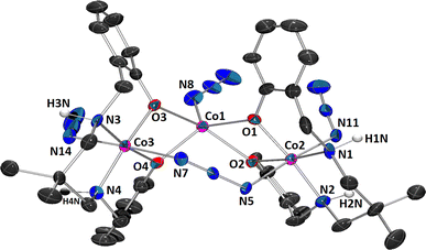
Each of the two terminal cobalt(III) centers Co(2) and Co(3), has a six-coordinate pseudo-octahedral geometry. For Co(2) centre, oxygen atoms, O(1), O(2) and nitrogen atoms, N(1) and N(2) of the deprotonated ligand (L)2− constitute the equatorial plane, and a nitrogen atom, N(5) of the bridging azide and another nitrogen atom, N(11) of a terminal azide, define the axial sites. Similarly, for Co(3) centre, oxygen atoms, O(3), O(4) and nitrogen atoms, N(3) and N(4) of the deprotonated ligand (L)2− constitute the equatorial plane, and a nitrogen atom, N(7) of the end-to-end bridging azide and another nitrogen atom, N(14) of a terminal azide, define the axial positions. On the other hand, the central cobalt(II) center, Co(1), is five coordinated being bonded to four phenoxo oxygen atoms {O(1), O(2), O(3) and O(4)} and one terminal azide nitrogen atom {N(8)}. The geometry of this cobalt(II) center is best described as an intermediate of trigonal bipyramidal and square pyramidal geometry, as confirmed by calculating Addison parameter, τ = 0.49, β = ∠O(2)–Co(1)–O(3) = 151.5° and α = ∠O(1)–Co(1)–N(8) = 122.3°, where α and β are the two largest L–L–L angles in the coordination sphere of the metal.42 The perspective view of CoO5N moiety with the largest L–M–L angles is shown in Fig. 2. Only one similar complex is reported in literature, which has been synthesized using 1,3-diaminopropane instead of 2,2-dimethyl-1,3-diaminopropane.43
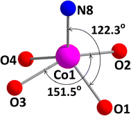 | ||
| Fig. 2 The perspective view of CoO5N moiety showing the largest L–M–L angles in the coordination sphere. | ||
The Co(2)⋯Co(1) distances are not sufficiently short enough {3.093(3) Å} to imply any cobalt–cobalt bonding.23,39 The bridging angles, ∠Co(1)–O(1)–Co(2) = 104.3(4)°, ∠Co(1)–O(2)–Co(2) = 99.8(4)°, ∠Co(1)–O(3)–Co(3) = 100.9(3)° and ∠Co(1)–O(4)–Co(3) = 102.9(4)° indicate that the cobalt(III)–O–cobalt(II) fragments are non-collinear. Cobalt(II)–O distances vary from 2.013(9) to 2.099(8) Å (Table 2), values equivalent to those observed in other high-spin cobalt(II) complexes.22 The cobalt(III)-oxygen and cobalt(III)-nitrogen distances (Table 2) are in the range 1.897(8)–1.943(10) and 1.907(11)–1.989(12)Å, respectively, which are typical for low-spin cobalt(III).22 Both the saturated six membered chelate rings, Co(2)–N(1)–C(8)–C(9)–C(12)–N(2) and Co(3)–N(3)–C(27)–C(28)–C(31)–N(4), represent chair conformations (Fig. 3) with puckering parameters,44 Q = 0.540(15) Å, θ = 18.6(14)°, φ(2) = 182(4)° and Q = 0.551(13) Å, θ = 161.7(12)°, φ(2) = 359(4)°, respectively.
IR and electronic spectra
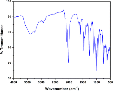
The IR and electronic spectra of the complex are in excellent concurrence with its crystal structure. A distinct band is observed in the IR spectrum of the complex at 3394 cm−1 due to O–H stretching vibrations of lattice methanol molecule.43 A moderately sharp band around 3236 cm−1 corresponding to the presence of N–H stretching vibrations and absence of any peak around ∼1600 cm−1 (corresponding to imine vibration) indicates that the azomethine groups of the Schiff base has been reduced prior to the complex formation.17,36 The band corresponding to the alkyl C–H stretching can be observed in the range of 2874–2922 cm−1 for the complex.17,23,36,39 A very strong double band observed at 2012 and 2081 cm−1 confirms the presence of two types of azide groups (bridging and terminal, respectively) in the complex.45 The IR spectrum of the complex is given in Fig. 4.The electronic spectrum of the complex in acetonitrile medium consists of three most fundamental bands for the complex. The high-energy, intense bands around 265 nm with hump (232 nm) for the complex, may be due to intra-ligand π–π* transition.23,39 Moreover, the intense absorption band at 357 nm in the complex is assigned to charge transfer transitions from the coordinated ligands to the cobalt(II) centers (LMCT).23,39 A weak band around 640 nm for the complex may be assigned as one of the two expected transitions for cobalt(II) complex in octahedral geometry.31 The transitions from cobalt(III) may get obscured by other bands. The electronic spectrum of the complex is given in Fig. 5.
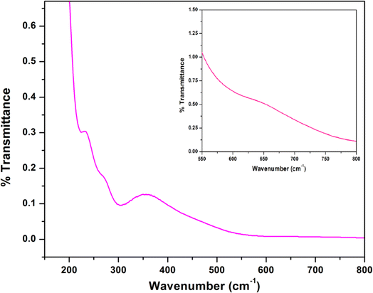 | ||
| Fig. 5 Electronic spectrum of the complex in acetonitrile. Inset shows the absorption band for low spin cobalt(III) center in the complex. | ||
Magnetic properties
The room temperature magnetic moment of the complex is 5.1 BM, which suggests that the complex contains just one high-spin cobalt(II) centre. This data, therefore, agree well with the representation of the complex as Co(III)(S = 0)–Co(II)(S = 3/2)–Co(III)(S = 0) trimer.23,39 The calculation of the spin density on the cobalt centres in each complex also supports this assignment of oxidation states (vide infra).Spin density
Spin density serves as a metric for gauging the spatial distribution of the disparity between the number of alpha (spin-up) and beta (spin-down) electrons within a quantum system. Essentially, it quantifies the degree to which a specific region in a molecule or solid is more inclined to host electrons with one spin orientation over the other. By examining the spin density of the scrutinized complex, we can deduce the localization of unpaired electrons.The findings reveal that within this complex, the unpaired alpha electrons are predominantly situated around the central cobalt center, linked to four oxygen atoms and the N3− ligand, exhibiting a spin population of 2.68. Meanwhile, the remaining cobalt centers exhibit fully paired electrons, resulting in a spin population of approximately zero. To facilitate a clear visualization of spin density, two plots are presented in Fig. 6 to depict the results. Mulliken Spin population and atomic charge of the investigated complex are given in Table S3 in ESI.†
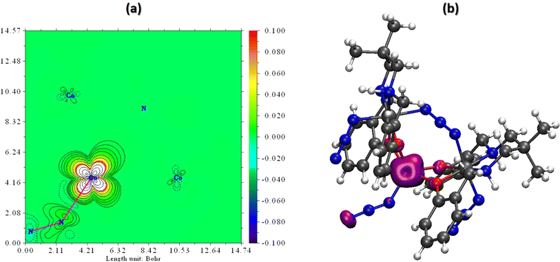 | ||
| Fig. 6 (a) Spin density plot and (b) spin density fill-contour map plot in a plane of the complex. The red zone clearly indicates the presence of unpaired electrons. | ||
Electrochemical studies
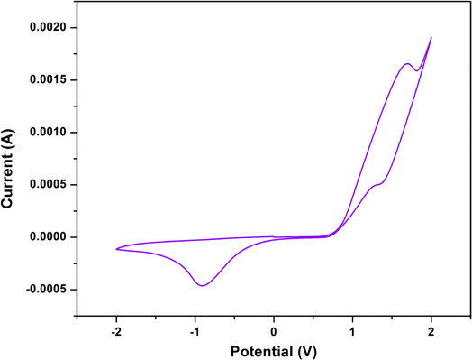
Using cyclic voltammetry (CV) in DMF with 10−3 M of each complex having tetrabutylammonium bromide (TBAB) as supporting electrolyte, the redox behaviour of the synthesized complex was examined.Cyclic voltammetric studies of the complex display two one-electron cyclic voltammetric responses. From them, one is quasi-reversible redox signal and another is irreversible redox signal. The quasi-reversible redox signal consists of an oxidation peak, Epa at +1.69 V and a reduction peak, Epc at +1.34 V, whereas the irreversible signal consists only a reduction peak, Epc at −0.92 V. The quasi-reversible redox signal could be attributed to the CoII → CoIII oxidation and the CoIII → CoII reduction, whereas the irreversible signal could be attributed to the CoIII → CoII reduction only. The cyclic voltammograms of the complex is shown in Fig. 7. The cyclic voltammetric results are consistent with those of other trinuclear mixed valence complexes of cobalt that have been reported in the literature.17,38,46,47 The detailed electrochemical data for the complex is given in Table 4.
| Scan rate (mV s−1) | Epa (V) (CoII → CoIII) | Epc (V) (CoIII → CoII) | E1/2 (V) (CoII ↔ CoIII) | ΔEp (CoII ↔ CoIII) | Epc (V) (CoIII → CoII) |
|---|---|---|---|---|---|
| a E1/2 denotes the half-wave potential. E1/2 = (Epa + Epa)/2 and ΔEp = (Epa − Epc). | |||||
| 200 | +1.69 | +1.34 | +1.51 | +0.35 | −0.92 |
Optical properties
The optical band gap (Eg) of the complex is determined with the help of Tauc's equation, which corresponds to the electronic transition from the valence band to the conduction band.48 From Tauc's equation, we used,| (αhν)n = A(hν − Eg) | (1) |
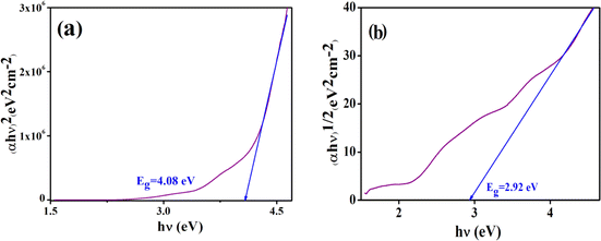 | ||
| Fig. 8 Tauc plot to evaluate the direct (a) and indirect (b) allowed band gap energy of the complex. | ||
Electrical characterization
The calculated optical band gap offers that material is in the family of a semiconducting in nature. It propelled us to study the semiconducting properties of our material. Hence, we have developed our as-synthesized cobalt based metal (Al)–semiconductor (MS) junction thin film device. The device has been developed following the method50 (see ESI†). The current–voltage (I–V) relationship of fabricated devices have been studied in dark as well as illumination (Intensity ∼100 mW cm−2) conditions at room temperature (300 K) at corresponding applied bias voltage sequentially within the limit ±1 V to analyze the charge transport behaviour. All the study was carried out under N2 filled glove box and laboratory temperature of 27 °C.The I–V characteristic of the cobalt based devices has been recorded under dark and illumination condition (Fig. 9). Under dark condition, the electrical conductivity of the cobalt based device has been calculated as 1.05 × 10⁻⁶ S m−1. However, after exposed under illumination, the conductivity of the same device has been calculated as 2.12 × 10⁻⁶ S m−1. It is clear that the conductivity of the synthesized complex based device improves considerably in illumination conditions from the non-illuminated condition.
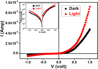 | ||
| Fig. 9 I–V characteristics curve for cobalt based/Al structured thin film devices under dark and photo illumination condition. | ||
Besides, the illustrative I–V characteristics of the Al/cobalt based interface under both dark and a photo illumination condition (Fig. 9) represents a nonlinear rectifying behaviour, like Schottky diode (SD). Under photo illumination condition, our material based device exhibits larger current which is the significance of photosensitivity. Hence, we have measured the photosensitivity of our device which has been found to be 0.93.
Here, we have estimated the thermionic emission theory to analyze the obtained I–V characteristics of cobalt based SDs. In this regard Cheung's method is also been employed to extract important diode parameters51–54 (see ESI† for detail studies).
The ideality factor (η) and the series resistance (RS) of our fabricated device have been calculated from the intercept and the slope of dV/dln![[thin space (1/6-em)]](https://www.rsc.org/images/entities/char_2009.gif) I vs. I plot (Fig. 10) under both conditions. The obtained value of ideality factor of the device both under dark and irradiation conditions has been listed below in Table 5. The value of ideality factor (η) of the fabricated SD has been estimated as 1.17 and 1.11 under dark and illumination condition respectively. The calculated values of ideality factor of the device under both conditions shows a deviation from its ideal value (∼1). The existence of interface states and series resistance at the junction and presence of inhomogeneities of Schottky barrier height may be the main factor for this non-ideal behaviour.54,55
I vs. I plot (Fig. 10) under both conditions. The obtained value of ideality factor of the device both under dark and irradiation conditions has been listed below in Table 5. The value of ideality factor (η) of the fabricated SD has been estimated as 1.17 and 1.11 under dark and illumination condition respectively. The calculated values of ideality factor of the device under both conditions shows a deviation from its ideal value (∼1). The existence of interface states and series resistance at the junction and presence of inhomogeneities of Schottky barrier height may be the main factor for this non-ideal behaviour.54,55
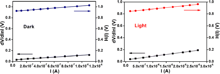 | ||
Fig. 10 dV/dln![[thin space (1/6-em)]](https://www.rsc.org/images/entities/char_2009.gif) I vs. I curve and H(V) vs. I curve for our synthesized cobalt based thin film device under dark, and photo illumination condition. I vs. I curve and H(V) vs. I curve for our synthesized cobalt based thin film device under dark, and photo illumination condition. | ||
| Condition | Conductivity (S m−1) | Photosensitivity | Ideality factor (η) | Barrier height (eV) | Avg. RS from dV/dln![[thin space (1/6-em)]](https://www.rsc.org/images/entities/char_2009.gif) I & H (kΩ) I & H (kΩ) |
|---|---|---|---|---|---|
| Dark | 1.05 × 10⁻⁶ | 0.93 | 1.17 | 0.78 | 90 |
| Light | 2.12 × 10⁻⁶ | 1.11 | 0.75 | 52.5 |
However, under photo illumination condition the ideality factor of the fabricated SD approaches more ideal (near to the value 1), which is a significant observation. This incident represents the less recombination of interfacial charge carriers and generation of better homogeneity at the barrier of Schottky junctions.51 From this analysis, it may be concluded that the synthesized cobalt complex based SD possesses fewer number of carrier recombination at the junction i.e. better barrier homogeneity even under illumination condition.
We have calculated the value of barrier height (ϕB) from the intercept of H(I) vs. I plot (Fig. 10). In this study the barrier potential height of the device represents a reduction under irradiation condition, which has the significance. This reduction may be occurred due to the accumulation of the produced photo induced charge carriers near the conduction band. The slope of H(I) vs. I plot also gives the series resistance (RS). The measured potential height (ϕB), ideality factor (η) and series resistance (RS) under dark and illumination condition for the metal (Al)–semiconductor (cobalt based material) (MS) junctions have been listed in Table 5. The diminution of RS due to expose under the irradiation condition of our device signifies its applicability in the field of optoelectronics.
For an in-depth analysis of the charge transport phenomena at MS junction, we have further studied the I–V curves. The characteristic I–V curves under both conditions in the logarithmic scale reveal that it can be differentiated in two regions (region I and region II) having different slope values (Fig. 11).
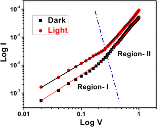 | ||
Fig. 11 log![[thin space (1/6-em)]](https://www.rsc.org/images/entities/char_2009.gif) V vs. log V vs. log![[thin space (1/6-em)]](https://www.rsc.org/images/entities/char_2009.gif) I curves for the as-synthesized cobalt based thin film device under dark and illumination condition. I curves for the as-synthesized cobalt based thin film device under dark and illumination condition. | ||
The first region (Region-I), with the slope value is ∼1, symbolizes to the ohmic regime. Here the generated current follows the relation I ∝ V. In which portion the current is proportional to V2 that is called as second region (Region-II) (Fig. 11). Here the value of slope is about 2, which is the characteristic of a trap free space charge limited current (SCLC) regime.51,56 If the injected carriers are more than the background carriers, the injected carriers spread and generate a space charge field. In this region the currents are controlled by this space charge field and are known as SCLC.51,56 The device performance was estimated by adopting SCLC theory.
Following this model, the effective carrier mobility has been estimated from higher voltage region of I vs. V2 plot (Fig. 12) by Mott–Gurney equation.51,54,56
 | (2) |
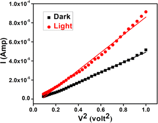 | ||
| Fig. 12 I vs. V2 curves for the synthesized cobalt based thin film device under dark and illumination condition. | ||
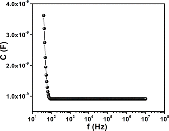
The relative dielectric constant has been estimated as 2.47, measured from the plot of capacitance against frequency (Fig. 13) of synthesized cobalt based film format at constant bias potential.
Further we have calculated the transit time (τ). These are some major parameters to analyze charge transport across the junction. From the slope of SCLC region (region-II) of Fig. 11, using the following equations we have estimated τ.51,57
 | (3) |
All the parameters estimated in the SCLC region demonstrate that the charge transport properties of the material improve under illumination condition (Table 6). The higher mobility implied higher transport rate under illumination, while the number of charge carriers also increased under the same condition. The diode parameters of the synthesized complex based SD demonstrate superior charge transfer kinetics under irradiation condition.
| Condition | εr | μeff (m2 V−1 s−1) | τ (sec) | μeff τ (m2 V−1) |
|---|---|---|---|---|
| Dark | 2.47 | 3.02 × 10⁻⁷ | 2.55 × 10⁻⁶ | 7.701 × 10⁻¹³ |
| Light | 5.33 × 10⁻⁷ | 1.46 × 10⁻⁶ | 7.782 × 10⁻¹³ |
The absence of region having slope higher than 2 in the IV characteristics can be attributed to the limited voltage range considered in our analysis, specifically in the positive voltage region. In the presented data, we focused on the voltage range up to 1 V, in which the slope of the 0–0.25 V range was found to be approximately 1 (ohmic region) and subsequently the slope as 2 (SCLC region).
Here, we would like to mention that extending the positive voltage range might reveal additional regions with higher slopes, more indicative of exponential behavior. Also, it is to be noted that, the I–V characteristic behavior of any diode not only depends on the applied voltage range, but also on the nature of the constituting materials.
It's crucial that the absence of higher slope regions within the explored voltage range doesn't imply a non-exponential nature. The diode exhibits exponential characteristics in the observed range, having the value of the slope as 1, and subsequently 2. Thus, the limited range of the positive voltage axis does not negate the overall exponential nature of the diode's behavior.
The comparison of electrical parameters of our synthesized complex with some other cobalt complexes17,40,58,59 reported in literature is given in Table 7. It demonstrates that our synthesized complex exhibits photosensitivity whereas the other reported complexes do not. The ideality factor value, on the other hand, indicates that our synthesized complex produced a more ideal diode than other reported complexes. So, these kinds of materials can pave the way for a very promising future in optoelectronic device application.
| Cobalt complexes used in Schottky diode | Condition | Photosensitivity | Device conductivity (S m−1) | Ideality factor | Barrier height (eV) | Rectification ratio | Reference |
|---|---|---|---|---|---|---|---|
| a H2L1 = [1,3-bis(2-hydroxybenzylamino)2,2-dimethylpropane] and H2L2 = [2,2'-[1,1'-(propane-2,2-diyldiimino)diethylidene]diphenol], H2L3 = [(2,2-dimethyl-1,3-propanediyl)bis(iminomethylene)bis(6-methoxyphenol)], H2L4 = [(2,2-dimethyl-1,3-propanediyl)bis(iminomethylene)bis(6-ethoxyphenol)], HO2CR1 = 3-methyl-4-nitrobenzoic acid, HO2CR2 = 4-methyl-3-nitrobenzoic acid, H2adc = acetylenedicarboxylic acid, 4-ppy = 4-phenylpyridine and 4-bppy = 4-(4-bromophenyl)-pyridine). | |||||||
| [CoII(N3){CoIII(μ-L)(N3)}2(μ-N3)]·MeOH | Dark | 0.93 | 1.05 × 10⁻⁶ | 1.17 | 0.78 | 90 | This work |
| Light | 2.12 × 10⁻⁶ | 1.11 | 0.75 | 52.5 | |||
| [CoII{(μ-L1)(μ-OAc)CoIII(OAc)}2]·2.67H2O | Dark | — | 5.858 × 10⁻⁴ | 1.826 | 0.596 | 44.326 | 17 |
| [CoII{(μ-L1)(μ-OOCPh)CoIII(DMSO)0.8(OOCPh)0.2}2](ClO4)1.6 | — | 6.804 × 10⁻⁵ | 2.144 | 0.645 | 6.164 | 17 | |
| [CoII{(μ-L2)(μ-OOCPh)CoIII(DMSO)0.75(OOCPh)0.25}2](ClO4)1.5 | — | 9.358 × 10⁻⁵ | 1.911 | 0.644 | 6.381 | 17 | |
| [(N3)CoIIIL3(μ-C6H4(NO2)CO2)CoII(N3)] | Dark | — | 2.04 × 10⁻⁵ | 1.13 | 0.69 | 14 | 56 |
| [(N3)CoIIIL4(μ-C6H4(NO2)CO2)CoII(N3)] | — | 2.58 × 10⁻⁴ | 1.12 | 0.62 | 36 | 56 | |
| [(H2O)CoIIL3(μ-O2CR1)CoII(NCS)] | Dark | — | 2.04 × 10⁻⁵ | 1.82 | 0.72 | — | 57 |
| [(DMSO)CoIIL4(μ-O2CR2)CoII(NCS)] | — | 1.54 × 10⁻³ | 0.76 | 0.58 | — | 57 | |
| [Co(adc)(4-ppy)(H2O)2]n | Dark | — | 2.61 × 10⁻⁵ | 3.08 | 0.75 | 112.47 | 38 |
| [Co(adc)(4-bppy)(H2O)2]n | — | 2.52 × 10⁻⁶ | 2.15 | 0.79 | 18.59 | 38 | |
It may be interesting to compare the electrical parameters of the present complex with some other complexes of different transition and non-transition metals with different Schiff bases and their reduced analogues. Table 8 gathers the electrical properties of these complexes. This demonstrates that our synthesized mixed valence cobalt complex is showing higher conductivity, better rectification ratio and better ideality factor than many of other reported complexes.
| Transition and non-transition metals complexes used in Schottky diode | Condition | Photosensitivity | Device conductivity (S m−1) | Ideality factor | Barrier height (eV) | Rectification ratio | Reference |
|---|---|---|---|---|---|---|---|
| a HL5 = [2-methoxy-6-((E)-(quinolin-3-ylimino)methyl)phenol], HL6 = [2-methoxy-6-((E)-(quinolin-5-ylimino)methyl)phenol], H2L7 = [ N,N′-bis(5-bromosalicylidene)-2,2-dimethyl-1,3-propanediamine], HL8 = (E)-N′-(thiophen-2-ylmethylene)isonicotinohydrazide, H2bdc = 1,4-benzene dicarboxylic acid, ppmh = N-pyridin-2-yl-N′-pyridin-4-ylmethylene-hydrazine, H2L9 = N,N-bis(3-methoxysalicylidene)propane-1,3-diamine, H2L10 = 2-[(2-dimethylamino-ethylamino)-methyl]-4-nitrophenol, H2L11 = 2-[(2-diethylamino-ethylamino)-methyl]-4-nitrophenol. | |||||||
| {[Cd2(HL5)2(N(CN)2)2]·H2O}n | Dark | 2.89 | 1.78 × 10⁻⁷ | 2.75 | 0.42 | 15.48 | 60 |
| Light | 6.15 × 10⁻⁷ | 2.35 | 0.38 | 46.23 | |||
| [Cd(HL6)2(N(CN)2)2]n | Dark | 2.54 | 1.07 × 10⁻⁷ | 2.96 | 0.44 | 14.73 | 60 |
| Light | 2.44 × 10⁻⁷ | 2.62 | 0.41 | 37.69 | |||
| [(N3)CoL7Na(N3)]n | Dark | 1.45 | 0.88 × 10⁻⁸ | 0.27 | 0.90 | 25.57 | 14 |
| Light | 2.38 × 10⁻⁸ | 0.91 | 0.87 | 135.49 | |||
| {[Zn(HL8)2]·DMF}n | Dark | — | 2.53 × 10⁻⁹ | 2.04 | 0.39 | — | 61 |
| Light | 5.97 × 10⁻⁵ | 1.88 | 0.21 | — | |||
| [Zn4(bdc)4(ppmh)2(H2O)]n | Dark | 20.95 | 6.20 × 10⁻⁷ | 3.41 | 0.60 | 93 | 62 |
| Light | 1.37 × 10⁻⁶ | 2.91 | 0.58 | 32 | |||
| [{CuL9Na}2(μ-1,1,3-NCS)HgCl(μ-Cl)(μ-1,3-NCS)]n | Dark | 57 | 1.48 × 10⁻⁶ | 0.35 | 0.71 | 21.66 | 16 |
| Light | 8.40 × 10⁻⁵ | 0.58 | 0.62 | 30.75 | |||
| [Cu(L10)(μ1,3-N3)]∞ | Dark | — | 12.54 × 10⁻⁵ | 2.25 | 1.16 | 3 | 63 |
| Light | 20.94 × 10⁻⁵ | 1.59 | 0.60 | 129 | |||
| [Cu2(L11)2(μ1,1-N3)(μ1,3-N3)]∞ | Dark | — | 13.45 × 10⁻⁵ | 3.21 | 0.63 | 4.31 | 63 |
| Light | 28.14 × 10⁻⁵ | 1.27 | 0.62 | 104 | |||
Band gap and density of states of the investigated complex
The difference in energy between the highest occupied and lowest unoccupied MOs (Δε = ELUMO − EHOMO, eV) is sometimes assumed as the band gap. We calculated Δε by DFT calculations as shown in Fig. 14. The calculated band gaps are 2.54 eV (from α-HOMO–α-LUMO) and 2.49 eV (from β-HOMO–β-LUMO) for the complex. The results show that the band gaps resulting from α-FMOs for the complex agree with the ranges of experimental values as shown in Fig. 8, respectively. Fig. 14 shows the total and partial DOS calculations, which clearly state that the valence band is mainly dominated by the d-orbitals of the cobalt atoms. In this complex, both in the valence band and conduction band, the contribution of the s- and p-orbitals is poor.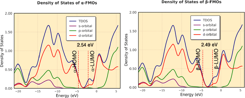 | ||
| Fig. 14 The total and partial DOS calculations of the valence and conduction bands for α- and β-FMOs of the complex. | ||
Summary and conclusion
The synthesis and characterization of a trinuclear cobalt(III/II/III) complex with N2O2 donor reduced Schiff base ligand have been described in the present paper. Single crystal X-ray diffraction has confirmed its structure. More flexibility of the reduced Schiff bases compared to their Schiff base precursor may be the driving force in forming the complex, as the non-reduced analogue of the Schiff bases fails to prepare the complex. Electrochemical measurements were performed in DMF solution to account for the redox behavior of the complex. The band gap of this semiconductor material in the solid state has been determined and it confirms that it is a semiconductor. We have also shown the potential of this complex in fabricating a photosensitive Schottky device. Theoretical studies have been used to rationalize the experimental observations and to provide an explanation to the enhanced conductivity of the complex upon illumination. It is a promising candidate to have applications in semiconducting research and in the fabrication of optoelectronic devices.Conflicts of interest
There are no conflicts to declare.Acknowledgements
S. B. thanks UGC, India for providing Senior Research Fellowship. We are thankful to Prof. Saurabh Das, Jadavpur University to help us in collecting the CV data.References
- K. Lu, C. Zhao, L. Luan, J. Duan, Y. Xie, M. Shao and B. Hu, J. Mater. Chem. C, 2018, 6, 5055–5062 RSC
.
- S.-J. Kim and J.-S. Lee, Nano Lett., 2010, 10, 2884–2890 CrossRef CAS PubMed
.
- K.-J. Baeg, M. Binda, D. Natali, M. Caironiand and Y.-Y. Noh, Adv. Mater., 2013, 25, 4267–4295 CrossRef CAS PubMed
.
- E. Najafi, M. M. Amini, E. Mohajerani, M. Janghouri, H. Razavi and H. Khavasi, Inorg. Chim. Acta, 2013, 399, 119–125 CrossRef CAS
.
- R. C. Evans, P. Douglas and C. J. Winscom, Coord. Chem. Rev., 2006, 250, 2093–2126 CrossRef CAS
.
- G. Wu, J. Huang, Y. Zang, J. He and G. Xu, J. Am. Chem. Soc., 2017, 139, 1360–1363 CrossRef CAS PubMed
.
- W. Chen, H.-M. Yuan, J.-Y. Wang, Z.-Y. Liu, J.-J. Xu, M. Yang and J.-S. Chen, J. Am. Chem. Soc., 2003, 125, 9266–9267 CrossRef CAS PubMed
.
- C. E. Patrick and F. Giustino, Adv. Funct. Mater., 2011, 21, 4663–4667 CrossRef CAS
.
- S. Roy, A. Dey, P. P. Ray, J. Ortega-Castro, A. Frontera and S. Chattopadhyay, Chem. Commun., 2015, 51, 12974–12976 RSC
.
- S. Khan, S. Halder, A. Dey, B. Dutta, P. P. Ray and S. Chattopadhyay, New J. Chem., 2020, 44, 11622–11630 RSC
.
- S. Roy, A. Dey, M. G. B. Drew, P. P. Ray and S. Chattopadhyay, New J. Chem., 2019, 43, 5020–5031 RSC
.
- S. Roy, A. Dey, R. M. Gomila, J. Ortega-Castro, A. Frontera, P. P. Ray and S. Chattopadhyay, Dalton Trans., 2022, 51, 5721–5734 RSC
.
- S. Roy, S. Halder, A. Dey, K. Harms, P. P. Ray and S. Chattopadhyay, New J. Chem., 2020, 44, 1285–1293 RSC
.
- K. Ghosh, S. Sil, P. P. Ray, J. Ortega-Castroc, A. Frontera and S. Chattopadhyay, RSC Adv., 2019, 9, 34710–34719 RSC
.
- S. Khan, S. Halder, P. P. Ray, S. Herrero, R. González-Prieto, M. G. B. Drew and S. Chattopadhyay, Cryst. Growth Des., 2018, 18, 651–659 CrossRef CAS
.
- S. Roy, S. Halder, M. G. B. Drew, P. P. Ray and S. Chattopadhyay, New J. Chem., 2018, 42, 15295–15305 RSC
.
- S. Bhunia, P. Das, S. Banerjee, R. M. Gomila, M. G. B. Drew, A. Frontera, P. P. Ray and S. Chattopadhyay, New J. Chem., 2023, 47, 14202–14216 RSC
.
- T. Basak, D. Das, P. P. Ray, S. Banerjee and S. Chattopadhyay, CrystEngComm, 2020, 22, 5170–5181 RSC
.
- F. Ahmed, B. Dutta and M. H. Mir, Dalton Trans., 2021, 50, 29–38 RSC
.
- S. Halder, Adv. Mater., 2023, 4, 5033–5049 RSC
.
- B. Dutta, F. Ahmed and M. H. Mir, Dalton Trans., 2023, 52, 17084–17098 RSC
.
- T. G. Dastidar and S. Chattopadhyay, Polyhedron, 2022, 211, 115511 CrossRef CAS
.
- S. Chattopadhyay, M. G. B. Drew and A. Ghosh, Eur. J. Inorg. Chem., 2008, 1693–1701 CrossRef CAS
.
- J. Welby, L. N. Rusere, J. M. Tanski and L. A. Tyler, Inorg. Chim. Acta, 2009, 362, 1405–1411 CrossRef CAS
.
- G. E. Assey, R. J. Butcher and Y. Gultneh, Acta Crystallogr., 2011, E67, m303–m304 Search PubMed
.
- E. Baca-Solis, S. Bern`es, H. Vazquez-Lima, M.-E. Boulon, R. E. P. Winpenny and Y. Reyes-Ortega, ChemistrySelect, 2016, 1, 6866–6871 CrossRef CAS
.
- L.-W. Wang, Q.-G. Shang, J.-J. Zhou, H. Zhou, Z.-Q. Pan and Q.-R. Cheng, Chin. J. Inorg. Chem., 2018, 34, 957 CAS
.
- S. Banerjee, J.-T. Chen and C.-Z. Lu, Polyhedron, 2007, 26, 686–694 CrossRef CAS
.
- T. R. J. Achard, W. Clegg, R. W. Harrington and M. North, Tetrahedron, 2012, 68, 133–144 CrossRef CAS
.
- K. Ghosh, K. Harms, A. Bauzá, A. Frontera and S. Chattopadhyay, CrystEngComm, 2018, 20, 7281–7292 RSC
.
- A. Hazari, A. Das, P. Mahapatra and A. Ghosh, Polyhedron, 2017, 134, 99–106 CrossRef CAS
.
- X. He, C.-Z. Lu and C.-D. Wu, J. Coord. Chem., 2006, 59, 977–984 CrossRef CAS
.
- C. Fukuhara, E. Asato, T. Shimoji and K. Katsura, J. Chem. Soc., Dalton Trans., 1987, 1305–1311 RSC
.
- L. Mechi, P. Siega, R. Dreos, E. Zangrando and L. Randaccio, Eur. J. Inorg. Chem., 2009, 2629–2638 CrossRef CAS
.
- J. Tang, F. Huang, Y. Wei, H. Bian, W. Zhang and H. Liang, Dalton Trans., 2016, 45, 8061–8072 RSC
.
- S. Bhunia, R. M. Gomila, A. Frontera and S. Chattopadhyay, Polyhedron, 2022, 223, 115910 CrossRef CAS
.
- S. Bhunia, R. M. Gomila, A. Frontera and S. Chattopadhyay, Inorganica Chim. Acta, 2023, 547, 121324 CrossRef CAS
.
- S. Bhunia and S. Chattopadhyay, Results Chem., 2023, 5, 100701 CrossRef CAS
.
- S. Chattopadhyay, G. Bocelli, A. Musatti and A. Ghosh, Inorg. Chem. Commun., 2006, 9, 1053–1057 CrossRef CAS
.
- F. Ahmed, J. Datta, S. Khan, B. Dutta, S. Islam, S. Naaz, P. P. Ray and M. H. Mir, New J. Chem., 2020, 44, 9004–9009 RSC
.
- M. Reinhardt, S. Dalgleish, Y. Shuku, L. Reissig, M. M. Matsushita, J. Crain, K. Awaga and N. Robertson, Phys. Chem. Chem. Phys., 2017, 19, 6768–6776 RSC
.
- A. G. Blackman, E. B. Schenk, R. E. Jelley, E. H. Krensked and L. R. Gahan, Dalton Trans., 2020, 49, 14798–14806 RSC
.
- P. Bhowmik, H. P. Nayek, M. Corbella, N. Aliaga-Alcalde and S. Chattopadhyay, Dalton Trans., 2011, 40, 7916–7926 RSC
.
- D. Cremer and J. A. Pople, J. Am. Chem. Soc., 1975, 97, 1354–1358 CrossRef CAS
.
- A. Hazari, L. K. Das, R. M. Kadam, A. Bauzá, A. Frontera and A. Ghosh, Dalton Trans., 2015, 44, 3862–3876 RSC
.
- M. Das and S. Chattopadhyay, Polyhedron, 2013, 50, 443–451 CrossRef CAS
.
- S. Chattopadhyay, G. Bocelli, A. Musatti and A. Ghosh, Inorg. Chem. Commun., 2006, 9, 1053–1057 CrossRef CAS
.
- J. Tauc, Amorphous and Liquid Semiconductors, Plenum Press, New York, 1974 Search PubMed
.
- J. Datta, M. Das, S. Sil, S. Kumara, A. Dey, R. Jana, S. Bandyopadhyay and P. P. Ray, Mater. Sci. Semicond. Process., 2019, 91, 133–145 CrossRef CAS
.
- S. Saha, M. Das, K. S. Das, R. Datta, S. Bala, J.-L. Liu, P. P. Ray and R. Mondal, Cryst. Growth Des., 2023, 23, 1104–1118 CrossRef CAS
.
- S. A. J. Boyce, J. Moutet, L. Niederegger, T. Simler, G. Nocton and C. R. Hess, Inorg. Chem., 2021, 60, 403–411 CrossRef CAS PubMed
.
- E. H. Rhoderick, Metal–Semiconductor Contacts, Oxford University, Press, London, 1978 Search PubMed
.
- S. K. Cheung and N. W. Cheung, Appl. Phys. Lett., 1986, 49, 85–87 CrossRef CAS
.
- D. Das, M. Das, S. Sil, P. Sahu and P. P. Ray, ACS Omega, 2022, 7, 26483–26494 CrossRef CAS
.
- X. Miao, S. Tongay, M. K. Petterson, K. Berke, A. G. Rinzler, B. R. Appleton and A. F. Hebard, Nano Lett., 2012, 12, 2745–2750 CrossRef CAS
.
- P. W. M. Blom, M. J. M. de Jong and M. G. V. Munster, Phys. Rev. B: Condens. Matter Mater. Phys., 1997, 55, R657–R659 CrossRef
.
- M. Das, D. Das, S. Sil and P. P. Ray, Nanoscale Adv., 2023, 5, 3655–3663 RSC
.
- A. Banerjee, D. Das, P. P. Ray, S. Banerjee and S. Chattopadhyay, Dalton Trans., 2021, 50, 1721–1732 RSC
.
- R. S. Sarkar, A. Biswas, P. P. Ray, R. M. Gomila, M. G. B. Drew, S. Banerjee, A. Frontera and S. Chattopadhyay, CrystEngComm, 2023, 25, 1006–1017 RSC
.
- P. Ghorai, A. Dey, A. Hazra, B. Dutta, P. Brandão, P. P. Ray, P. Banerjee and A. Saha, Cryst. Growth Des., 2019, 19, 6431–6447 CrossRef CAS
.
- K. Debsharma, S. Dey, D. Das, S. Halder, J. Ortega-Castro, S. Sarkar, B. Dutta, S. Maity, K. Jana, A. Frontera, P. P. Ray and C. Sinha, CrystEngComm, 2023, 25, 162–172 RSC
.
- A. Chandra, M. Das, K. Pal, S. Jana, B. Dutta, P. P. Ray, K. Jana and C. Sinha, ACS Omega, 2019, 4, 17649–17661 CrossRef CAS PubMed
.
- M. Mondal, S. Jana, M. G. B. Drew and A. Ghosh, Polymer, 2020, 204, 122815 CrossRef CAS
.
Footnote |
| † Electronic supplementary information (ESI) available: Physical measurement, X-ray crystallography, Hirshfeld surface analysis, noncovalent interactions, band gap measurement from CV, device fabrication, electrical characterization, BVS calculation, Fig. S1–S7 and Tables S1–S3. CCDC 2305257. For ESI and crystallographic data in CIF or other electronic format see DOI: https://doi.org/10.1039/d4ra01406e |
| This journal is © The Royal Society of Chemistry 2024 |


