DOI:
10.1039/D4RA04602A
(Paper)
RSC Adv., 2024,
14, 25852-25864
Microstructure evolution, dielectric properties, and nonlinear response of Na+-doped CdCu3Ti4O12 ceramics
Received
24th June 2024
, Accepted 2nd August 2024
First published on 16th August 2024
Abstract
In this study, Cd1−xNaxCu3Ti4O12 (x = 0, 0.02, 0.04, 0.06, and 0.08) ceramics were prepared via a solid-state method. The phase composition, microstructure, and defect characteristics as well as optical, dielectric, and nonlinear properties of the ceramics were systematically studied. A CuO second phase was detected in doped samples. Grain boundary precipitates, Na with a low melting point, and oxygen and cation vacancies together caused the grain size to first increase and then decrease with an increase in the Na+ doping amount. The abundant emerging cation vacancies with an increase in Na+ content led to a decrease in the optical energy band. The sample with x = 0.04 exhibited the highest ε′ value (∼35![[thin space (1/6-em)]](https://www.rsc.org/images/entities/char_2009.gif) 800) due to its largest grain size. Moreover, it possessed a lower tan
800) due to its largest grain size. Moreover, it possessed a lower tan![[thin space (1/6-em)]](https://www.rsc.org/images/entities/char_2009.gif) δ (∼0.053) at 10 kHz, which was attributed to the multiplication of insulating grain boundaries. The huge dielectric constant originated from Maxwell–Wagner polarization at low frequencies and followed the internal barrier effect model. The lowest tan
δ (∼0.053) at 10 kHz, which was attributed to the multiplication of insulating grain boundaries. The huge dielectric constant originated from Maxwell–Wagner polarization at low frequencies and followed the internal barrier effect model. The lowest tan![[thin space (1/6-em)]](https://www.rsc.org/images/entities/char_2009.gif) δ (∼0.037) and optimal nonlinear properties (α = 3.66 and Eb = 3.82 kV cm−1) were obtained in the sample with x = 0.08, which were associated with its highest grain boundary resistance and barrier height. Electric modulus data proved that dielectric relaxation at low frequencies was associated with grain boundaries. Dielectric anomalies in the high temperature range were attributed to oxygen vacancies.
δ (∼0.037) and optimal nonlinear properties (α = 3.66 and Eb = 3.82 kV cm−1) were obtained in the sample with x = 0.08, which were associated with its highest grain boundary resistance and barrier height. Electric modulus data proved that dielectric relaxation at low frequencies was associated with grain boundaries. Dielectric anomalies in the high temperature range were attributed to oxygen vacancies.
1. Introduction
CaCu3Ti4O12 (CCTO) has a high dielectric constant (104) at low frequencies, which remains stable in the temperature range from 100 to 600 K.1–3 This peculiarity makes it able to increase the storage capacity per unit volume and reduce the size of the device, which is of great importance in dynamic memory, 5G communication, and energy storage fields.4,5 Unlike other perovskite materials, the high dielectric constant of CCTO is not due to the dipole polarization mechanism but due to the Maxwell–Wagner polarization based on semiconducting grains and insulating grain boundaries.3,6,7 With the continuous progress in research, such materials have formed a large ACu3Ti4O12 family (ACTO, A = Ca, Cd, Bi2/3, Y2/3, La2/3, etc.).1,8–11 However, in this type of material, a higher dielectric constant (ε′) usually means a greater dielectric loss (tan![[thin space (1/6-em)]](https://www.rsc.org/images/entities/char_2009.gif) δ). Therefore, exploring the origin of the large dielectric constant and searching for possibilities to increase dielectric constant while maintaining low dielectric loss is an urgent task. Notably, owing to their electrically heterogeneous structure and high barrier, grain boundaries produce nonlinear current–voltage properties, which are appealing for varistors.12–14
δ). Therefore, exploring the origin of the large dielectric constant and searching for possibilities to increase dielectric constant while maintaining low dielectric loss is an urgent task. Notably, owing to their electrically heterogeneous structure and high barrier, grain boundaries produce nonlinear current–voltage properties, which are appealing for varistors.12–14
CdCu3Ti4O12 (CdCTO) is a member of ACTO-type materials. The first achieved dielectric constant of CdCTO was only 409 at 105 Hz.1 After improving the preparation process, a large dielectric constant (104) could be attained.15,16 Subsequently, Mg2+, Zn2+, Zr4+, and other elements were used as dopants in CdCTO.17–21 Peng et al. reported high ε′ values (>4 × 10⁴) at a relatively low tan![[thin space (1/6-em)]](https://www.rsc.org/images/entities/char_2009.gif) δ (<0.1) at 1 kHz in CdCu2.9Zn0.1Ti4O12 and CdMg0.1Cu2.9Ti4O12 ceramics.17,18 Nonlinear coefficient (α) and breakdown field strength (Eb) are two very important parameters of varistors. Peng et al. observed an improvement in both parameters from α ∼3.15 and Eb ∼0.257 kV cm−1 for CdCTO to α ∼4.98 and Eb ∼1.78 kV cm−1 for 3.0 wt% Al2O3-doped CdCTO ceramics and to Eb ∼2.36 kV cm−1 for 4.0 wt% SiO2-doped CdCTO ceramics, respectively, although the additives led to a decrease in dielectric constant.20,21 In general, the current research on the dielectric properties of CdCTO is still at its initial stage, especially in terms of the nonlinear properties. Therefore, the development of advanced methods to optimize the dielectric and nonlinear properties is essential for large-scale applications of CdCTO materials.
δ (<0.1) at 1 kHz in CdCu2.9Zn0.1Ti4O12 and CdMg0.1Cu2.9Ti4O12 ceramics.17,18 Nonlinear coefficient (α) and breakdown field strength (Eb) are two very important parameters of varistors. Peng et al. observed an improvement in both parameters from α ∼3.15 and Eb ∼0.257 kV cm−1 for CdCTO to α ∼4.98 and Eb ∼1.78 kV cm−1 for 3.0 wt% Al2O3-doped CdCTO ceramics and to Eb ∼2.36 kV cm−1 for 4.0 wt% SiO2-doped CdCTO ceramics, respectively, although the additives led to a decrease in dielectric constant.20,21 In general, the current research on the dielectric properties of CdCTO is still at its initial stage, especially in terms of the nonlinear properties. Therefore, the development of advanced methods to optimize the dielectric and nonlinear properties is essential for large-scale applications of CdCTO materials.
Ion doping or substitution is one of the important means to improve the ACTO properties. Among them, Na+ doping of A-sites in ACTO has been reported. In Na+-doped La2/3Cu3Ti4O12 and Y2/3Cu3Ti4O12 ceramics, the grain size varied in an unpredictable manner, while increasing continuously in Bi2/3Cu3Ti4O12 and CaCu3Ti4O12 ceramics.22–25 The optimal dielectric properties (ε′ ∼97![[thin space (1/6-em)]](https://www.rsc.org/images/entities/char_2009.gif) 647 and tan
647 and tan![[thin space (1/6-em)]](https://www.rsc.org/images/entities/char_2009.gif) δ ∼0.073) were attained in the Ca0.98Na0.02Cu3Ti4O12 ceramic, exceeding those of the Na0.35Bi0.55Cu3Ti4O12 (ε′ ∼7600 and tan
δ ∼0.073) were attained in the Ca0.98Na0.02Cu3Ti4O12 ceramic, exceeding those of the Na0.35Bi0.55Cu3Ti4O12 (ε′ ∼7600 and tan![[thin space (1/6-em)]](https://www.rsc.org/images/entities/char_2009.gif) δ ∼0.015), Na0.05Y0.65Cu3Ti4O12 (ε′ ∼7500 and tan
δ ∼0.015), Na0.05Y0.65Cu3Ti4O12 (ε′ ∼7500 and tan![[thin space (1/6-em)]](https://www.rsc.org/images/entities/char_2009.gif) δ ∼0.022), and Na0.5La0.5Cu3Ti4O12 (ε′ ∼15
δ ∼0.022), and Na0.5La0.5Cu3Ti4O12 (ε′ ∼15![[thin space (1/6-em)]](https://www.rsc.org/images/entities/char_2009.gif) 000 and tan
000 and tan![[thin space (1/6-em)]](https://www.rsc.org/images/entities/char_2009.gif) δ ∼0.047) ceramics, respectively.22–25 Meanwhile, the effects of Na+ on the microstructure and dielectric properties of the above materials were poorly understood, in spite of the fact that doping generally improves the dielectric properties. This meant that the underlying mechanism of doping in relation to performance was unclear. Moreover, the nonlinear electrical properties of these materials were not explored. In addition, very few studies have been focused on CdCTO ceramics with different proportions of Na+ doping. In this work, Cd1−xNaxCu3Ti4O12 (x = 0, 0.02, 0.04, 0.06, and 0.08) ceramics were prepared via solid-state reaction method. The effect of Na+ doping on the microstructure, optical and dielectric characteristics, complex impedance behavior, and nonlinear properties of ceramics was systematically investigated. The optimized dielectric and nonlinear properties were shown to provide more options for the application of ACTO materials. The relevant mechanism affecting the microstructure of Cd1−xNaxCu3Ti4O12 ceramics may be fundamental for further clarification of the origin of the large dielectric response in ACTO ceramics.
δ ∼0.047) ceramics, respectively.22–25 Meanwhile, the effects of Na+ on the microstructure and dielectric properties of the above materials were poorly understood, in spite of the fact that doping generally improves the dielectric properties. This meant that the underlying mechanism of doping in relation to performance was unclear. Moreover, the nonlinear electrical properties of these materials were not explored. In addition, very few studies have been focused on CdCTO ceramics with different proportions of Na+ doping. In this work, Cd1−xNaxCu3Ti4O12 (x = 0, 0.02, 0.04, 0.06, and 0.08) ceramics were prepared via solid-state reaction method. The effect of Na+ doping on the microstructure, optical and dielectric characteristics, complex impedance behavior, and nonlinear properties of ceramics was systematically investigated. The optimized dielectric and nonlinear properties were shown to provide more options for the application of ACTO materials. The relevant mechanism affecting the microstructure of Cd1−xNaxCu3Ti4O12 ceramics may be fundamental for further clarification of the origin of the large dielectric response in ACTO ceramics.
2. Materials and methods
2.1. Powders and ceramics preparation
Cd1−xNaxCu3Ti4O12 (x = 0, 0.02, 0.04, 0.06, and 0.08) ceramics were prepared via solid-state method. The starting materials were CdO (99%), NaCO3 (99.99%), CuO (99%), and TiO2 (99%) (all purchased from Shanghai Aladdin Biochemical Technology Co., Ltd). Precursors were mixed proportionally, and ground with an agate mortar for 3 h. The obtained powders were afterward calcined at 800 °C for 10 h, ground for 3 h with the addition of 2 wt% PVA, and pressed into disk-shaped pellets with 10 mm diameter and 1 mm thickness at 8 MPa. Pellets were first sintered at 550 °C for 2 h to remove PVA, and then at 1000 °C for 15 h in air at the heating rate of 3 °C min−1. Prior to electric measurements, both sides of specimens were coated with silver paste and heated at 300 °C for 20 min.
2.2. Structural and electrical property characterization
The crystal structure and phase composition of specimens were analyzed via X-ray diffraction (XRD, SmartLab, Rigaku, Japan; Cu-Kα radiation (λ = 1.5418 Å)) and Raman spectroscopy (Renishaw InVia, UK; 532 nm laser excitation wavelength). The Rietveld refinement of XRD profiles was performed in the GSAS software. The densities of specimens were assessed via Archimedes' method. The microstructure and elemental compositions of ceramics were characterized via field emission scanning electron microscopy (FE-SEM, JSM-7000F, Japan). The average grain size was determined from the FE-SEM images using the Nano Measurer software. The overall chemical composition was determined from inductively coupled plasma mass spectroscopy (ICPMS, Agilent 7700, USA). Dried Cd1−xNaxCu3Ti4O12 starting powders and sintered ceramic powders of 30–50 mg were dissolved in 25 ml of an aqua regia and hydrofluoric acid mixture, and diluted with deionized water by 1 and 100 times, respectively, for Na and other elements prior to analysis. The positron annihilation lifetime spectra were recorded to establish the defect characteristics by means of a fast–fast coincidence lifetime spectrometer (ORTEC, USA); prior to the experiment, a 22Na positron source was sandwiched between two specimens of the same composition. During the measurements, more than 106 counts were collected. The PALS fit software was used for data processing. Ultraviolet-visible (UV-vis) spectroscopy (UH4150, China) was employed to obtain the absorption characteristics of the specimens. The dielectric and complex impedance spectra of ceramics were measured with a precision impedance analyzer (Agilent 4294A, USA). The current density–electric field (J–E) characteristics were acquired with the Keithley 2400 test system. The nonlinearity coefficients α were calculated according to the following formula: α = log(J2/J1)/log(E2/E1), where E1 and E2 are the voltages at currents J1 = 0.1 mA and J2 = 1 mA, respectively. The Eb values were obtained at J1 = 1 mA cm−2.
2.3. First-principles calculation details
The first-principles calculations were carried out to evaluate the stability of Cd1−xNaxCu3Ti4O12 crystal structures by using the Cambridge Serial Total Energy Package code.26 The interactions between electrons and ionic nuclei were modeled by means of Vanderbilt-type ultrasoft pseudopotentials so as to establish the electronic structure of the specimen.27 The generalized gradient approximation based on the Perdew–Burke–Ernzerhof functional was performed to evaluate the exchange correlation energy.28 The energy of the first Brillouin zone was calculated using a 4 × 4 × 4 K-point grid in Monkhorst–Pack format, whereby the cutoff energy of the plane wave base set of the electron wave function was 340 eV.
3. Results and discussion
Fig. 1(a) depicts the XRD patterns of the Cd1−xNaxCu3Ti4O12 ceramics. The major diffraction peaks were ascribed to the body-centered cubic perovskite (JCPDS card no. 75-2188), corresponding to the CCTO phase. A CuO second phase appeared in the samples with x = 0.02 and 0.04. The lattice distortion was caused by the substitution of Na+ ions (r6 = 1.02 Å) for Cd2+ (r6 = 0.95 Å),29 which promoted the formation of a Cu-rich grain boundary layer.23,30 According to the CaO–CuO–TiO2 ternary system, the compound CCTO appeared to be a “point compound” with very narrow solubility limits.31 When the composition deviated slightly from perfect stoichiometry, the material ended up along a binary tie-line or inside a ternary field, resulting in the second phases in the microstructure of CCTO.31 This resulted in the precipitation of the CuO phase in the ACTO material.31,32 Similar results were also reported in the CdO–CuO–TiO2 ternary system.33 The CuO second phase observed in the samples with x = 0.02 and 0.04 should be closely related to the Cd site component deviation caused by Na doping. The Rietveld refinement of the XRD spectra was further carried out to obtain detailed information about the lattice parameters of the Cd1−xNa2xCu3Ti4O12 ceramics (the results are displayed in Table 1 and Fig. 1(b)). It was evident that the simulated curves effectively matched the experimental data, indicating decent reliability of the refinement. The unit cell parameter of CdCTO was found to be 7.3839 Å, and coincided with the value reported in ref. 15. This parameter increased in specimens with x = 0.02 and 0.04, owing to the larger ionic radius of the dopant.29 This meant that Na+ was successfully incorporated in the Cd sites of the CdCTO ceramics, forming a crystal structure of Cd1−xNa2xCu3Ti4O12, which is presented in Fig. 1(d). However, the unit cell parameter value decreased at x = 0.06 and 0.08. This is likely due to the limit of the Na solubility in Cd sites, and will be discussed later.
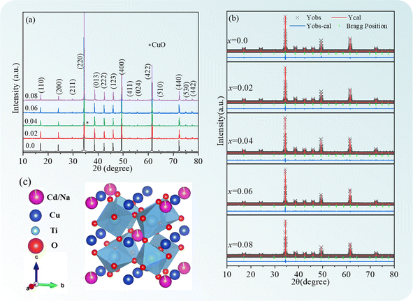 |
| | Fig. 1 (a) XRD patterns of Cd1−xNaxCu3Ti4O12 ceramics; Rietveld refinement plots in the case of (b) CdCTO and (c) BCTO; (d) crystal structure of Cd1−xNaxCu3Ti4O12. | |
Table 1 Structural data and relative densities of Cd1−xNaxCu3Ti4O12 ceramics
| Samples |
0.0 |
0.02 |
0.04 |
0.06 |
0.08 |
| Space group |
Im![[3 with combining macron]](https://www.rsc.org/images/entities/char_0033_0304.gif) |
Im![[3 with combining macron]](https://www.rsc.org/images/entities/char_0033_0304.gif) |
Im![[3 with combining macron]](https://www.rsc.org/images/entities/char_0033_0304.gif) |
Im![[3 with combining macron]](https://www.rsc.org/images/entities/char_0033_0304.gif) |
Im![[3 with combining macron]](https://www.rsc.org/images/entities/char_0033_0304.gif) |
| Unit cell parameters (Å) |
a = b = c 7.3823(6) |
a = b = c 7.3918(2) |
a = b = c 7.3921(2) |
a = b = c 7.3915(5) |
a = b = c 7.3815(3) |
| Volume (Å3) |
402.323 |
403.878 |
403.928 |
403.829 |
402.192 |
| R-Factors (%) |
Rp = 6.19 |
Rp = 5.69 |
Rp = 5.33 |
Rp = 4.89 |
Rp = 5.44 |
| Rwp = 8.04 |
Rwp = 7.34 |
Rwp = 6.49 |
Rwp = 6.16 |
Rwp = 6.97 |
| Relative density (%) |
χ2 = 2.015 |
χ2 = 1.649 |
χ2 = 1.465 |
χ2 = 1.235 |
χ2 = 1.575 |
| 93.9 |
94.5 |
95.8 |
95.2 |
95.1 |
The Raman spectra were collected to reveal the effect of Na+ doping on the Cd1−xNa2xCu3Ti4O12 ceramics. Because of the weak scattering of ACTO, only a few of the eight modes (2Ag + 2Eg + 4Fg) allowed by the selection rules appeared in the spectra.34 Fig. 2(a) displays the Raman spectra of the Cd1−xNaxCu3Ti4O12 ceramics in the wavenumber range of 100–900 cm−1, revealing the bands at 265, 330, 438, 506 and 571 cm−1. Among them, the peaks at 265, 330, 438 and 506 cm−1 correspond to Fg(1), Eg(1), Ag(1) and Ag(2) vibration modes originating from the TiO6 rotation, while the feature at 571 cm−1 was attributed to the Fg(3) vibration mode related to the O–Ti–O anti-stretching atomic motion in the TiO6 octahedron.34 The results are similar to those reported in ref. 8–20. The positions of three main peaks (Eg(1), Ag(1), and Ag(2)) remained unchanged with Na+ doping, which meant that Na+ had no effect on either the charge distribution or the Ti–O vibration in the TiO6 octahedron. Remarkably, the mode at 292 cm−1 at x = 0.04 was ascribed to the CuO phase,35 which was consistent with the XRD results. To further clarify the mode of the CuO phase in the specimens, Raman spectra were deconvoluted in the wavenumber range of 200–400 cm−1, as shown in Fig. 2(b). The results confirmed the existence of the CuO phase in other doped samples.
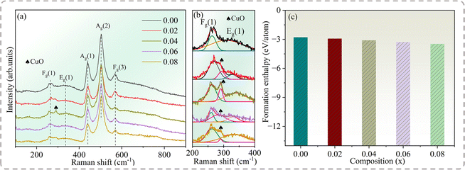 |
| | Fig. 2 (a) Raman spectra, (b) the deconvoluted Raman spectra and (c) formation enthalpy of the Cd1−xNaxCu3Ti4O12 ceramics determined via first-principles calculations. | |
The formation enthalpy can reflect the thermodynamic stability of the crystal structure. Based on the first-principles calculation, the formation enthalpy of the Cd1−xNaxCu3Ti4O12 ceramics can be obtained as follows:36
| |
 | (1) |
where Δ
Hf,
Etot,
Ni, and
Esolidi are the formation enthalpy, the total energy of the unit cell, the number of
i-th atoms in the unit cell, and the total energy of each atom of the pure element in its ground state, respectively.
Fig. 2(c) depicts the formation enthalpy of the Cd
1−xNa
xCu
3Ti
4O
12 ceramics. The negative value of CdCTO indicates its stable structure. With the increase of Na
+ doping, the Δ
Hf value tended to be more negative. As is known, the stability of a crystal structure increases with the increase of the negativity of the formation enthalpy.
36 Thus, this increased negative Δ
Hf value indicated the increase in structural stability of the doped samples.
Fig. 3 shows the cross-sectional SEM images of the Cd1−xNaxCu3Ti4O12 ceramics. The abnormally large grains and scattered small grains with scarce pores were clearly observed in CdCTO (Fig. 3(a)). The grain size increased with the increase of the Na+ doping content, achieving a maximum in the sample with x = 0.04. Notably, the increase in Na+ doping content caused a dramatic decrease in grain size. The average grain sizes at x = 0, 0.02, 0.04, 0.06, and 0.08 were 16.06 ± 3.12, 16.35 ± 3.03, 21.78 ± 4.22, 8.19 ± 1.14, and 6.37 ± 0.58 μm, respectively. The relative densities of the specimens are listed in Table 1, all exceeding 93% and indicating a dense structure.
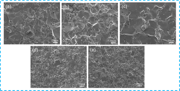 |
| | Fig. 3 Cross-sectional SEM images of Cd1−xNaxCu3Ti4O12 ceramics: (a) x = 0; (b) x = 0.02; (c) x = 0.04; (d) x = 0.06; (e) x = 0.08. | |
EDS was used to reveal the element distribution in the samples. Fig. 4(a) depicts the EDS spectrum of the polished and thermally etched surface of the sample with x = 0.04 (see the inset), in which all elements were observed. Fig. 4(b–f) display the corresponding elemental maps, showing that Ti and Cd elements were prevalent in the grain region, but were scarce at the GBs. In turn, the Na elements were uniformly distributed, and the CuO phase was abundant at the GBs. This is similar to the data acquired on the Na+-doped CCTO ceramics in study.22 In the ACTO-like materials, the abnormal grain growth is usually associated with the presence of the CuO phase at the grain boundaries as a sintering aid during the high temperature treatment.7,9,37–39 Similarly, Na2CO3 with a low melting point (∼850 °C) also acted as the source of the liquid phase and promoted the grain growth.22,23 In addition, due to the unbalanced charge between Cd2+ and Na+, oxygen vacancies were created, conforming to the reaction below:
| |
 | (2) |
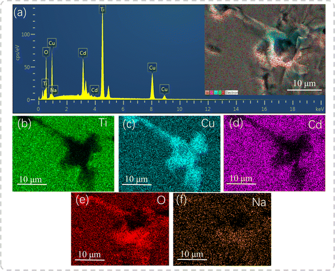 |
| | Fig. 4 (a) EDS spectrum at x = 0.04; the inset shows the polished and thermally etched surface of the sample; (b–f) elemental maps. | |
The oxygen vacancies promoted the grain boundary migration during the sintering process and increased the grain size. However, the grain size clearly decreased in the specimens with x = 0.06 and 0.08. This grain refinement might be due to excessive Na+ doping by analogy with that observed in the NaxLa(2−x)/3Cu3Ti4O12 and NaxY(2−x)/3Cu3Ti4O12 ceramics,23,25 which was not further interpreted. It was assumed that the intensive volatilization of Na with the low melting point in the sintering process might have produced the cation vacancies and inhibited the grain growth. To clarify the percentage for the chemical composition in the precursors and the sintered powders, ICPMS measurements were performed. The results are displayed in Table 2. The proportions of individual elements in the precursors (shown in parentheses) were consistent with those of Cd1−xNaxCu3Ti4O12. However, the proportions of Na were lower in the sintered powders, corresponding to the volatilization during the sintering process. Nevertheless, the Na content in the sintered samples increased with the increase of doping amount. Combined with the above reduced cell parameters in the samples with x = 0.06 and 0.08, it indicated that the solubility limit of Na in the Cd sites was exceeded. According to the phase diagram of the CdO–CuO–TiO2 system, the Cu-rich and Ti-rich phase existed at the grain boundary in CdxCu3Ti4O12 (x < 1) ceramics.33 Thus, a binary Na2O–TiO2 compound might incorporate all of the Na preferentially in the specimens with x = 0.06 and 0.08, which are located at the grain boundary and had a higher melting point to inhibit the grain growth.40 These second phases were not detected in the above XRD patterns and Raman spectra due to their small amount.
Table 2 Percentage for the chemical composition of the sintered powders (the precursors) determined via ICPMS
| Samples |
Element content (at mol%) |
| Na |
Cd |
Cu |
Ti |
| x = 0.0 |
0(0) |
4.96(5.01) |
14.94(15.02) |
21.12(20.04) |
| x = 0.02 |
0.06(0.09) |
4.83(4.88) |
14.96(15.05) |
21.10(20.06) |
| x = 0.04 |
0.12(0.18) |
4.71(4.75) |
14.97(15.02) |
21.14(20.11) |
| x = 0.06 |
0.18(0.28) |
4.61(4.64) |
14.95(15.02) |
21.16(20.09) |
| x = 0.08 |
0.23(0.37) |
4.48(4.52) |
14.96(15.04) |
21.18(20.05) |
The positron annihilation technique was employed to describe the cation vacancy characteristics of the specimens. In previous studies, the annihilation process within the ACTO ceramics has been interpreted in the context of the standard two-state trapping model.6,9,41 In this model, a short lifetime component τ1 is related to the positron annihilation in the bulk. Meanwhile, a long lifetime component τ2 represents the positron annihilation at the cation vacancy, where the electron density declines because of missing ions.42 The intensity I2 indicates the concentration of defects. In addition, the average lifetime (τave = τ1I1 + τ2I2) is a more reliable parameter reflecting the defect content. The τ1, τ2, I1, I2, and τave values of the Cd1−xNaxCu3Ti4O12 ceramics, obtained from the lifetime spectra, are listed in Table 3. Fig. 5 depicts the dependences of τ1, τ2, τave, and I2 on the Na+ content in the Cd1−xNaxCu3Ti4O12 ceramics. According to Fig. 5(a), the τ1 value of all of the samples remained almost constant. The τ2 and I2 values, as well as τave, continuously increased with the increase of Na+ doping content. This indicated that the size and number of cation vacancies in the doped samples increased. According to formula (2), Na+ did not increase the cation vacancy number. Thus, the increase in the amount of cation vacancies could be mainly associated with the volatilization of Na in the sintering process. Jumpatam et al. also reported the increase of vacancies caused by Na volatilization, which inhibited grain growth in Na1/3Ca1/3Y1/3Cu3Ti4O12 ceramics.43 With the increase of Na+ doping, the vacancy concentration continued to increase. This caused the cell shrinkage, which gradually counteracted the lattice expansion due to the presence of the Na+ dopant with the larger ion radius, eventually resulting in a smaller cell parameter for the sample with x = 0.08. This agreed with the XRD results depicted in Table 1. These cation vacancies inhibited the grain boundary migration and slowed down the grain growth.6,41 Thus, it can be concluded that the introduction of Na with the low melting point, along with the formation of the CuO phase and oxygen vacancies, was the main reason for the rapid grain growth at the Na+ doping amount less than 0.04. Meanwhile, the cation vacancies and the second phase containing Na inhibited grain growth at the doping amount above 0.04. Thus, the sample with x = 0.04 exhibited the largest grain size.
Table 3 Positron lifetime spectroscopy parameters for Cd1−xNaxCu3Ti4O12 ceramics
| Samples |
τ1 (ps) |
τ2 (ps) |
τave (ps) |
I1 (%) |
I2 (%) |
| x = 0.0 |
178.5 |
251.7 |
188.4 |
86.53 |
13.47 |
| x = 0.02 |
177.3 |
254.0 |
189.4 |
84.21 |
15.79 |
| x = 0.04 |
179.2 |
259.3 |
193.0 |
79.54 |
19.46 |
| x = 0.06 |
178.5 |
266.4 |
200.4 |
75.02 |
24.98 |
| x = 0.08 |
178.9 |
278.7 |
209.3 |
69.46 |
30.54 |
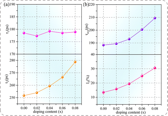 |
| | Fig. 5 (a) Positron lifetime components, τ1 and τ2; (b) τave and I2 as functions of the Na+ doping content in Cd1−xNaxCu3Ti4O12 ceramics. | |
UV-visible absorption spectroscopy was used to assess the optical properties and energy structure of the Cd1−xNaxCu3Ti4O12 ceramics. Fig. 6(a) depicts the UV-vis absorption spectra of all of the specimens in the wavelength range of 200–900 nm. The optical energy band (Eg) values were obtained using the Tauc method, as follows:44
where
hν,
α, and
k are the photon energy, the absorption coefficient, and a constant denoting the band edge parameter, respectively. The
Eg values determined by the
X-intercept of the tangent to the curve in
Fig. 6(b–f) were 4.18, 4.13, 4.11, 4.08, and 4.06 eV for
x = 0, 0.02, 0.05, 0.08, and 0.10, respectively, which were comparable with those of other ACTO-type ceramics.
8,45,46 Na
+ doping leads to an increase in the concentration of vacancies, thereby modulating the band structure and reducing the optical energy gap.
22,23 Therefore, these wide band-gap materials have great application potential in high-performance optoelectronic and electronic devices.
47,48
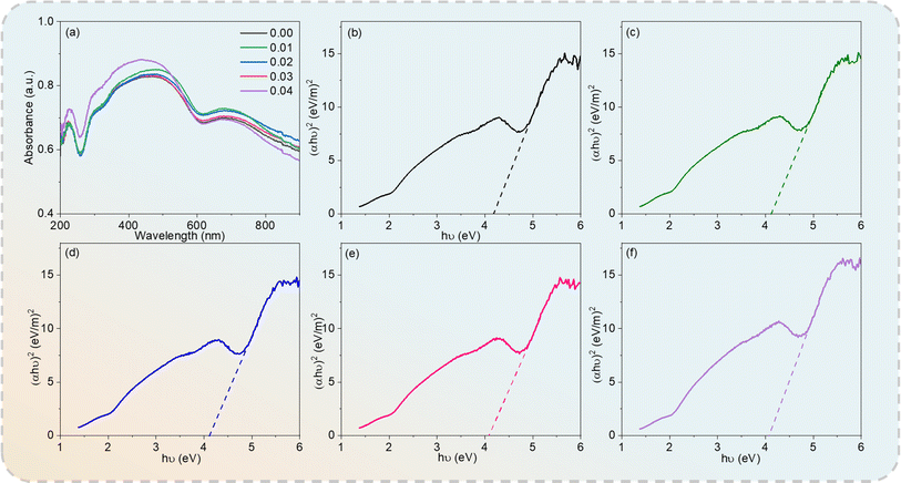 |
| | Fig. 6 (a) UV-vis absorption spectra of Cd1−xNaxCu3Ti4O12 ceramics and (αhν)2 versus hν plots at (b) x = 0.0; (c) x = 0.02; (d) x = 0.04; (e) x = 0.06; (f) x = 0.08. | |
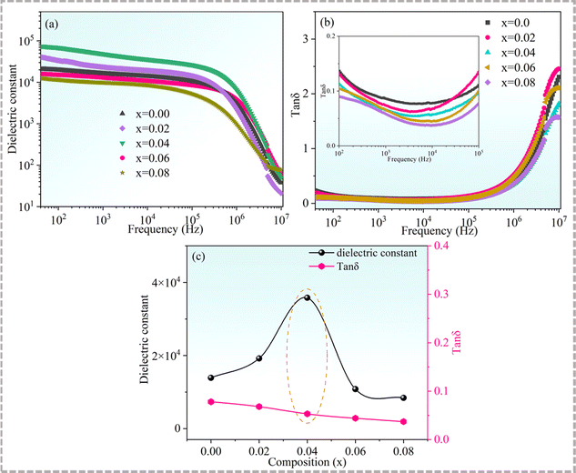
Fig. 7 displays the dependences of the dielectric constants and dielectric losses of Cd1−xNaxCu3Ti4O12 on the frequency. In general, the dielectric constants of all of the samples exhibited a plateau below 106 Hz, indicating good frequency stability. It then decreased sharply above 106 Hz, whereas a rapid increase of the dielectric loss occurred, which indicated a typical Maxwell–Wagner relaxation behavior.49 With the increase of Na+ doping content, the dielectric constant increased first and then decreased. According to the IBLC model, the dielectric constant is directly proportional to the grain size.50 The findings of the present study showed that the grain size and dielectric constant of the doped samples followed this relationship. The dielectric constants for Cd1−xNaxCu3Ti4O12 ceramics with x = 0, 0.02, 0.04, 0.06, and 0.08 at 10 kHz were 13![[thin space (1/6-em)]](https://www.rsc.org/images/entities/char_2009.gif) 900, 19
900, 19![[thin space (1/6-em)]](https://www.rsc.org/images/entities/char_2009.gif) 200, 35
200, 35![[thin space (1/6-em)]](https://www.rsc.org/images/entities/char_2009.gif) 800, 10
800, 10![[thin space (1/6-em)]](https://www.rsc.org/images/entities/char_2009.gif) 800, and 8400, respectively. Na+ doping also affected the dielectric loss of the samples. As seen from Fig. 7(b), the dielectric loss decreased with the increase of Na+ doping content. The corresponding values at 10 kHz for the Cd1−xNaxCu3Ti4O12 ceramics with x = 0, 0.02, 0.04, 0.06, and 0.08 were 0.078, 0.068, 0.053, 0.044, and 0.037, respectively. The dielectric constant of the sample with x = 0.04 increased by two and a half times (from 13
800, and 8400, respectively. Na+ doping also affected the dielectric loss of the samples. As seen from Fig. 7(b), the dielectric loss decreased with the increase of Na+ doping content. The corresponding values at 10 kHz for the Cd1−xNaxCu3Ti4O12 ceramics with x = 0, 0.02, 0.04, 0.06, and 0.08 were 0.078, 0.068, 0.053, 0.044, and 0.037, respectively. The dielectric constant of the sample with x = 0.04 increased by two and a half times (from 13![[thin space (1/6-em)]](https://www.rsc.org/images/entities/char_2009.gif) 900 to 35
900 to 35![[thin space (1/6-em)]](https://www.rsc.org/images/entities/char_2009.gif) 800) relative to that of the pure CdCTO, while the dielectric loss decreased to a small extent (from 0.078 to 0.053). Fig. 7(c) depicts the variation of the dielectric constant and dielectric loss at 10 kHz with the Na+ content. It was found that the sample with x = 0.04 had an optimal dielectric property. That is, sodium doping can not only reduce the dielectric loss but also increase the dielectric constant, which is consistent with the results achieved in the Na+-doped CCTO ceramics.39
800) relative to that of the pure CdCTO, while the dielectric loss decreased to a small extent (from 0.078 to 0.053). Fig. 7(c) depicts the variation of the dielectric constant and dielectric loss at 10 kHz with the Na+ content. It was found that the sample with x = 0.04 had an optimal dielectric property. That is, sodium doping can not only reduce the dielectric loss but also increase the dielectric constant, which is consistent with the results achieved in the Na+-doped CCTO ceramics.39
 |
| | Fig. 7 (a) Dielectric constant and (b) dielectric loss of Cd1−xNaxCu3Ti4O12 ceramics as functions of frequency; the inset presents the magnified view in the frequency range from 100 to 105 Hz; (c) dielectric constant and dielectric loss as a function of Na+ contents at 10 kHz. | |
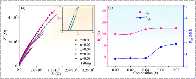
The complex impedance characteristics at room temperature were determined to elucidate the reasons for the variation of the dielectric properties of the Cd1−xNaxCu3Ti4O12 ceramics. Single semicircles with nonzero high-frequency intercepts were obtained (see Fig. 8 and the inset), where the low-frequency arc corresponded to the grain response and the high-frequency arc stood for the grain boundary response, respectively. An equivalent circuit model consisting of two parallel RC elements is usually used to simulate the impedance parameters. The grain resistance (Rg) and grain boundary resistance (Rgb) values of all samples, obtained using the ZsimpWin Version software, are presented in Fig. 8(b). The Rg value increased slightly in the range of 20 to 25 Ω, while the Rgb value dramatically increased with the increase of Na+ doping content. Semiconducting grains and insulating grain boundaries confirmed the electrical heterogeneity of all the samples. It is known that the lattice distortion resulting from the substitution ions with larger radii may promote the formation of a Cu-rich grain boundary layer, which can enhance the resistance of grain boundaries.23,30 Therefore, compared with the pure CdCTO, the specimens with x = 0.02 and 0.04 had higher Rgb values. The increase of Rgb caused by Na+ doping has also been reported in CCTO ceramics.39 In turn, the grain refinement increasing the number of grain boundaries has also caused the increase in Rgb at x = 0.06 and 0.08. Generally, the higher the grain boundary resistance is, the smaller the dielectric loss.3,6–10 The highest Rgb value obtained at x = 0.08 corresponded to the lowest tan![[thin space (1/6-em)]](https://www.rsc.org/images/entities/char_2009.gif) δ (∼0.037), while the lowest Rgb value of the CdCTO sample yielded the highest tan
δ (∼0.037), while the lowest Rgb value of the CdCTO sample yielded the highest tan![[thin space (1/6-em)]](https://www.rsc.org/images/entities/char_2009.gif) δ value (∼0.078) at 10 kHz.
δ value (∼0.078) at 10 kHz.
 |
| | Fig. 8 (a) Complex impedance plots of Cd1−xNaxCu3Ti4O12 ceramics at room temperature; the inset shows an expanded view of the high-frequency data close to the origin; (b) Rg and Rgb parameters as functions of x. | |
The dielectric function of the electric modulus was used to establish the mechanism of the dielectric response of the samples. The complex modulus M* can be expressed as follows:51
| |
 | (4) |
where
ε* is a complex dielectric constant; and
M′ and
M′′ are the real and imaginary parts of the complex modulus, respectively.
Fig. 9 depicts the frequency dependence of the electric modulus of the Cd
1−xNa
xCu
3Ti
4O
12 ceramics in the temperature range of 343−383 K. As seen from
Fig. 9, only a set of modulus peaks emerged in the frequency range of 40–10
5 Hz. For the samples with
x = 0.04 and 0.06, the modulus peaks moved out of the measuring frequency window at 343 K. Moreover, the electric modulus peaks shifted to higher frequencies with the increase of temperature, indicating a thermally activated mechanism in all of the specimens. The frequencies and temperatures of the modulus peaks follow the Arrhenius law:
52| |
 | (5) |
where
fmax,
f0,
Ea,
kb, and
T are the peak frequency, the pre-exponential factor, the activation energy, the Boltzmann constant, and the temperature, respectively. The electric modulus peaks of all of the samples are clearly identified in
Fig. 9. The inset of
Fig. 9 shows the ln
![[thin space (1/6-em)]](https://www.rsc.org/images/entities/char_2009.gif) fmax versus
fmax versus 1000/
T and the plots obtained by fitting using
eqn (5). The
Ea values for the Cd
1−xNa
xCu
3Ti
4O
12 ceramics were 0.609, 0.638, 0.657, 0.751, and 0.779 eV, respectively. These values were consistent with the grain boundary conductivity activation energy of the CdCTO ceramics obtained in ref.
17–19, confirming that the dielectric relaxation originated from grain boundaries. Therefore, it was concluded that the dielectric constant of the Cd
1−xNa
xCu
3Ti
4O
12 ceramics at low frequency was due to the Maxwell–Wagner relaxation in relation to grain boundaries.
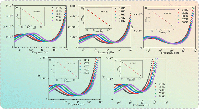 |
| | Fig. 9 Electric modulus (M′′) as a function of the frequency of Cd1−xNaxCu3Ti4O12 ceramics: (a) x = 0, (b) x = 0.02, (c) x = 0.04, (d) x = 0.06, and (e) x = 0.08. | |
To further study the thermally activated mechanism in the specimens, the temperature dependence of the dielectric constant for the Cd1−xNaxCu3Ti4O12 ceramics at 4, 6, 8, and 10 kHz is shown in Fig. 10. A set of the dielectric peaks emerged in the temperature range from 70 °C to 200 °C. The position of the peak shifted to higher temperature with the increase of frequency, while the peak intensity decreased in the specimens. The inset of Fig. 10 depicts the ln![[thin space (1/6-em)]](https://www.rsc.org/images/entities/char_2009.gif) fmax versus 1000/T plots fitted using eqn (5). The activation energy Ea values for the Cd1−xNaxCu3Ti4O12 ceramics with x = 0, 0.02, 0.04, 0.06, and 0.08 were 0.653, 0.682, 0.702, 0.733, and 0.754 eV, respectively, which were related to the oxygen vacancies and similar to the values reported in ref. 17, 19, 23 and 24. In addition, the relaxation activation energy was depressed by Na doping.
fmax versus 1000/T plots fitted using eqn (5). The activation energy Ea values for the Cd1−xNaxCu3Ti4O12 ceramics with x = 0, 0.02, 0.04, 0.06, and 0.08 were 0.653, 0.682, 0.702, 0.733, and 0.754 eV, respectively, which were related to the oxygen vacancies and similar to the values reported in ref. 17, 19, 23 and 24. In addition, the relaxation activation energy was depressed by Na doping.
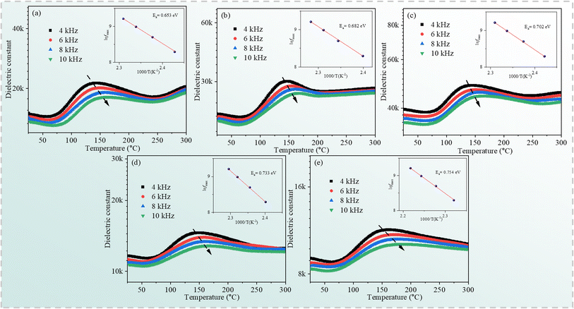 |
| | Fig. 10 Temperature dependence of the dielectric constant for the Cd1−xNaxCu3Ti4O12 ceramics (a) x = 0.0; (b) x = 0.02; (c) x = 0.04; (d) x = 0.06; (e) x = 0.08. | |
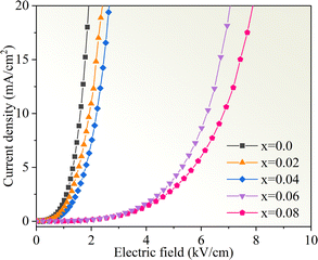
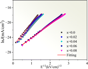
Fig. 11 displays the nonlinear current density–electric field (J–E) plots of the Cd1−xNaxCu3Ti4O12 ceramics. All samples exhibited good nonlinear characteristics. The corresponding α and Eb values were found to be 2.53, 2.99, 2.85, 3.04, 3.66, and 0.82, 0.93, 1.1, 3.47, and 3.82 kV cm−1 at x = 0, 0.02, 0.04, 0.06, and 0.08, respectively, surpassing those reported in ref. 20 and 21. For electrically heterogeneous ACTO materials, the nonlinear electrical properties usually originate from the Schottky barriers between the semiconducting grains and insulating grain boundaries.7,9,12,13 According to the Schottky model, the grain boundary barrier (Φb) can be obtained from the relationship between J and E as follows:53
| |
 | (7) |
where
A,
β,
kb, and
T are the Richardson's constant, the constant related to the potential barrier width, the Boltzmann constant, and the temperature, respectively.
Fig. 12 depicts the ln
![[thin space (1/6-em)]](https://www.rsc.org/images/entities/char_2009.gif) J versus E1/2
J versus E1/2 plots for the Cd
1−xNa
xCu
3Ti
4O
12 ceramics, which exhibited a good linear relationship and confirmed the existence of the Schottky barriers in all of the samples. According to the fitting results in
Fig. 12, the barrier heights (
Φb) were 0.679, 0.688, 0.708, 0.719, and 0.722 eV, respectively, at
x = 0, 0.02, 0.04, 0.06, and 0.08. These results were close to the
Egb values of the CCTO ceramics.
6,41 The variation of the barrier height was consistent with the grain boundary resistance and the activation energy
Ea. It is worth noting that the sample with
x = 0.08 possessed the optimal nonlinear properties due to its highest grain boundary resistance and barrier height. In addition, these
Φb values were comparable with the above activation energies
Ea, which confirmed that the dielectric relaxation in the low-frequency range originated from grain boundaries. To analyze the Na
+ doping effect on the dielectric properties and nonlinear response of the CdCTO specimens, a comparison of the
ε′, tan
![[thin space (1/6-em)]](https://www.rsc.org/images/entities/char_2009.gif) δ
δ,
α, and
Eb values of the Cd
1−xNa
xCu
3Ti
4O
12 ceramics with previously reported values in the literature is summarized in
Table 4. It is obvious that our Cd
1−xNa
xCu
3Ti
4O
12 ceramics exhibited greater dielectric and nonlinear properties than the ACTO-based ceramics.
 |
| | Fig. 11 Nonlinear J–E plots of the Cd1−xNaxCu3Ti4O12 ceramics. | |
 |
| | Fig. 12 The ln![[thin space (1/6-em)]](https://www.rsc.org/images/entities/char_2009.gif) J versus E1/2 plots for the Cd1−xNaxCu3Ti4O12 ceramics. J versus E1/2 plots for the Cd1−xNaxCu3Ti4O12 ceramics. | |
Table 4 Comparison of dielectric constant (ε′) and dielectric loss (tan![[thin space (1/6-em)]](https://www.rsc.org/images/entities/char_2009.gif) δ) at 1 or 10 kHz, the nonlinear coefficient (α) and breakdown field strength (Eb) of the Cd1−xNaxCu3Ti4O12 ceramics with previously reported values in the literature
δ) at 1 or 10 kHz, the nonlinear coefficient (α) and breakdown field strength (Eb) of the Cd1−xNaxCu3Ti4O12 ceramics with previously reported values in the literature
| Samples |
ε′ |
tan![[thin space (1/6-em)]](https://www.rsc.org/images/entities/char_2009.gif) δ δ |
α |
Eb |
Ref. |
| CdCTO |
2.4 × 10⁴ |
0.072 |
— |
— |
54 |
| Ca0.98Na0.02Cu3Ti4O12 |
9.8 × 10⁴ |
0.073 |
— |
— |
22 |
| CdMg0.1Cu2.9Ti4O12 |
5.0 × 10⁴ |
0.1 |
— |
— |
17 |
| Na0.35Bi0.55Cu3Ti4O12 |
0.76 × 10⁴ |
0.015 |
— |
— |
24 |
| CdCu2.9Zn0.1Ti4O12 |
4.0 × 10⁴ |
0.058 |
— |
— |
18 |
| Na0.5La0.5Cu3Ti4O12 |
1.5 × 10⁴ |
0.047 |
— |
— |
25 |
| Na0.05Y0.65Cu3Ti4O12 |
0.75 × 10⁴ |
0.022 |
— |
— |
23 |
| CdCTO-2.0wt%SiO2 |
0.52 × 10⁴ |
0.06 |
— |
1.90 |
21 |
| CdCTO-3wt%Al2O3 |
1.0 × 10⁴ |
0.1 |
4.89 |
1.78 |
20 |
| Cd0.96Na0.04Cu3Ti4O12 |
3.4 × 10⁴ |
0.053 |
2.85 |
1.10 |
This work |
| Cd0.94Na0.06Cu3Ti4O12 |
1.1 × 10⁴ |
0.044 |
3.04 |
3.47 |
This work |
| Cd0.92Na0.08Cu3Ti4O12 |
0.84 × 10⁴ |
0.037 |
3.66 |
3.82 |
This work |
4. Conclusions
In this study, Cd1−xNaxCu3Ti4O12 ceramics were prepared via the solid-state reaction method. Their phase composition, microstructure, and defect characteristics, as well as the optical, dielectric, and nonlinear properties were systematically investigated. In addition to the main Cd1−xNaxCu3Ti4O12 phase, the CuO second phase was found in the doped samples. The number of cation vacancies increased with the increase in Na+ doping content. Na with the low melting point, along with the formation of CuO phase and oxygen vacancies, was the main reason for the rapid grain growth at the Na+ doping amount of less than 0.04. Meanwhile, the cation vacancies and the second phase containing Na inhibited grain growth at the doping amount above 0.04. The optical energy band decreased with the multiplication of cation vacancies. The dielectric constant increased with the increase of grain size and followed the IBLC effect. The sample with x = 0.04 exhibited the highest ε′ value of ∼35![[thin space (1/6-em)]](https://www.rsc.org/images/entities/char_2009.gif) 800 and a lower tan
800 and a lower tan![[thin space (1/6-em)]](https://www.rsc.org/images/entities/char_2009.gif) δ of ∼0.053 at 10 kHz. The lowest tan
δ of ∼0.053 at 10 kHz. The lowest tan![[thin space (1/6-em)]](https://www.rsc.org/images/entities/char_2009.gif) δ of ∼0.037, along with the optimal nonlinear α and Eb values of ∼3.21 and ∼2.47 kV cm−1, respectively, was achieved in the sample with x = 0.08, which was associated with its highest grain boundary resistance and barrier height. Therefore, the electric modulus data proved that the large dielectric constant of the Cd1−xNaxCu3Ti4O1 ceramics was ascribed to the Maxwell–Wagner effect at the grain boundaries.
δ of ∼0.037, along with the optimal nonlinear α and Eb values of ∼3.21 and ∼2.47 kV cm−1, respectively, was achieved in the sample with x = 0.08, which was associated with its highest grain boundary resistance and barrier height. Therefore, the electric modulus data proved that the large dielectric constant of the Cd1−xNaxCu3Ti4O1 ceramics was ascribed to the Maxwell–Wagner effect at the grain boundaries.
Data availability
The data that support the findings of this study are available from the corresponding author upon reasonable request.
Conflicts of interest
No conflict of interest exists.
Acknowledgements
This work is supported by Key Research & Development and promotion projects in Henan Province (Project No. 242102241040) and Postgraduate Education Reform and Quality Improvement Project of Henan Province (No. YJS2023AL023), and by the University-Industry Collaborative Education Program of the Chinese Ministry of Education (No. 230702557130802).
References
- M. A. Subramanian, D. Li, N. Duan, B. A. Reisner and A. W. Sleight, High dielectric constant in ACu3Ti4O12 and ACu3Ti3FeO12 phases, J. Solid State Chem., 2000, 151, 323–325 CrossRef CAS.
- C. C. Homes, T. Vogt, S. M. Shapiro, S. Wakimoto and A. P. Ramirez, Optical response of high-dielectric-constant perovskite-related oxide, Science, 2001, 293, 673–676 CrossRef CAS PubMed.
- D. C. Sinclair, T. B. Adams, F. D. Morrison and A. R. West, CaCu3Ti4O12: One-step internal barrier layer capacitor, Appl. Phys. Lett., 2002, 80, 2153–2155 CrossRef CAS.
- Y. Wang, W. Jie, C. Yang, X. Wei and J. Hao, Colossal permittivity materials as superior dielectrics for diverse applications, Adv. Funct. Mater., 2019, 29, 323 Search PubMed.
- A. Chhetry, S. Sharma, H. Yoon, S. Ko and J. Y. Park, Enhanced sensitivity of capacitive pressure and strain sensor based on CaCu3Ti4O12 wrapped hybrid sponge for wearable applications, Adv. Funct. Mater., 2020, 30, 1910020 CrossRef CAS.
- R. Z. Xue, G. Y. Zhao, J. Chen, Z. P. Chen and D. W. Liu, Effect of doping ions on the structural defect and the electrical behavior of CaCu3Ti4O12 ceramics, Mater. Res. Bull., 2016, 76, 124–132 CrossRef CAS.
- R. Xue, L. Zhao, S. Chen, H. Chen, M. Cui, X. Bai, T. Li, D. Liu and H. Dai, Microstructural, dielectric, and nonlinear properties of Ca1–xCdxCu3Ti4O12 thin films, Ceram. Int., 2023, 49, 134–144 CrossRef CAS.
- Z. Peng, P. Liang, X. Wang, H. Peng, X. Chen, Z. Yang and X. Chao, Fabrication and characterization of CdCu3Ti4O12 ceramics with colossal permittivity and low dielectric loss, Mater. Lett., 2018, 210, 301–304 CrossRef CAS.
- R. Xue, L. Zhao, X. Liu, H. Wang, X. Zhu, Y. Xiao, C. Yuan, B. Cao, Z. Chen, T. Li and H. Dai, Enhanced optical, dielectric, and non-Ohmic properties in Ta-doped Bi2/3Cu3Ti4O12 ceramics, Solid State Sci., 2024, 150, 107495 CrossRef CAS.
- P. Liang, Z. Yang, X. Chao and Z. Liu, Giant dielectric constant and good temperature stability in Y2/3Cu3Ti4O12 ceramics, J. Am. Ceram. Soc., 2012, 95, 2218–2225 CrossRef CAS.
- M. M. Ahmad, H. M. Kotb, C. Joseph, S. Kumar and A. Alshoaibi, Transport and dielectric properties of mechanosynthesized La2/3Cu3Ti4O12 ceramics, Crystals, 2021, 11, 313 CrossRef CAS.
- S. Y. Chung, I. D. Kim and S. J. L. Kang, Strong nonlinear current-voltage behaviour in perovskite-derivative calcium copper titanate, Nat. Mater., 2004, 3, 774–778 CrossRef CAS PubMed.
- P. Leret, J. F. Fernandez, J. de Frutos and D. Fernández-Hevia, Nonlinear I–V electrical behaviour of doped CaCu3Ti4O12 ceramics, J. Eur. Ceram. Soc., 2007, 27, 3901–3905 CrossRef CAS.
- R. Xue, L. Zhao, X. Liu, H. Wang, X. Zhu, Y. Ren, Y. Xiao, C. Yuan and B. Cao, Modification of the dual-function varistor-capacitor properties of Bi2/3Cu3Ti4O12 ceramic by doping with Sr0.99La0.01TiO3, Mater. Today Commun, 2024, 39, 108823 CrossRef CAS.
- R. Zuo, L. Feng, Y. Yan, B. Chen and G. Cao, Observation of giant dielectric constant in CdCu3Ti4O12 ceramics, Solid State Commun., 2006, 138, 91–94 CrossRef CAS.
- Z. Peng, P. Liang, X. Wang, H. Peng, Y. Xiang, X. Chao and Z. Yang, Copper cadmium titanate prepared by different methods: Phase formation, dielectric properties and relaxor behaviors, Ceram. Int., 2018, 44, 7814–7823 CrossRef CAS.
- Z. Peng, P. Liang, J. Wang, X. Zhou, J. Zhu, X. Chao and Z. Yang, Interfacial effect inducing thermal stability and dielectric response in CdCu3Ti4O12 ceramics, Solid State Ionics, 2020, 348, 115290 CrossRef CAS.
- Z. Peng, D. Wu, P. Liang, X. Zhou, J. Wang, J. Zhu, X. Chao and Z. Yang, Grain boundary engineering that induces ultrahigh permittivity and decreased dielectric loss in CdCu3Ti4O12 ceramics, J. Am. Ceram. Soc., 2020, 103, 1230–1240 CrossRef CAS.
- Z. Peng, P. Liang, Y. Xiang, H. Peng, X. Chao and Z. Yang, Effect of Zr doping on dielectric properties and grain boundary response of CdCu3Ti4O12 ceramics, Ceram. Int., 2018, 44, 20311–20321 CrossRef CAS.
- Z. Peng, J. Wang, X. Zhou, J. Zhu, X. Lei, P. Liang, X. Chao and Z. Yang, Grain engineering inducing high energy storage in CdCu3Ti4O12 ceramics, Ceram. Int., 2020, 46, 14425–14430 CrossRef CAS.
- Z. Peng, J. Wang, F. Zhang, S. Xu, X. Lei, P. Liang, L. Wei, D. Wu, X. Chao and Z. Yang, High energy storage and colossal permittivity CdCu3Ti4O12 oxide ceramics, Ceram. Int., 2022, 48, 4255–4260 CrossRef CAS.
- P. Thongbai, K. Meeporn, T. Yamwong and S. Maensiri, Extreme effects of Na doping on microstructure, giant dielectric response and dielectric relaxation behavior in CaCu3Ti4O12 ceramics, Mater. Lett., 2013, 106, 129–132 CrossRef CAS.
- P. Liang, X. Chao and Z. Yang, Low dielectric loss, dielectric response, and conduction behavior in Na-doped Y2/3Cu3Ti4O12 ceramics, J. Appl. Phys., 2014, 116, 044101 CrossRef.
- L. Yang, X. Chao, P. Liang, L. Wei and Z. Yang, Electrical properties and high-temperature dielectric relaxation behaviors of NaxBi(2-x)/3Cu3Ti4O12 ceramics, Mater. Res. Bull., 2015, 64, 216–222 CrossRef CAS.
- Z. Liu and Z. Yang, Structure and electric properties of NaxLa(2-x)/3Cu3Ti4O12 ceramics prepared by sol–gel method, J. Mater. Sci.: Mater. Electron., 2018, 29, 9326–9338 CrossRef CAS.
- M. D. Segall, L. J. D. Philip, M. J. Probert, C. J. Pickard, P. J. Hasnip, S. J. Clark and M. C. Payne, First-principles simulation: ideas, illustrations and the CASTEP code, J. Phys. Condens. Matter, 2002, 14, 2717–2744 CrossRef CAS.
- J. S. Lin, A. Qteish, M. C. Payne and V. V. Heine, Optimized and transferable nonlocal separable ab initio pseudopotentials, Phys. Rev. B: Condens. Matter Mater. Phys., 1993, 47, 4174–4180 CrossRef PubMed.
- J. P. Perdew, K. Burke and M. Ernzerhof, Generalized gradient approximation made simple, Phys. Rev. Lett., 1996, 77, 3865–3868 CrossRef CAS PubMed.
- R. D. Shannon, Revised effective ionic radii and systematic studies of interatomie distances in halides and chaleogenides, Acta Crystallogr., Sect. A: Found. Crystallogr., 1976, 32, 751 CrossRef.
- Z. Yang, Y. Zhang, Z. H. Lu, K. Zhang, R. Xiong and J. Shi, Electrical Conduction and Dielectric Properties of the Rb-doped CaCu3Ti4O12, J. Am. Ceram. Soc., 2013, 96, 806 CrossRef CAS.
- N. Kolev, R. P. Bontchev, A. J. Jacobson, V. N. Popov, V. G. Hadjiev, A. P. Litvinchuk and M. N. Iliev, Raman spectroscopy of CaCu3Ti4O12, Phys. Rev. B: Condens. Matter Mater. Phys., 2002, 66, 132102 CrossRef.
- S. Y. Lee, H. E. Kim and S. I. Yoo, Subsolidus phase relationship in the CaO–CuO–TiO2 ternary system at 950°C in air, J. Am. Ceram. Soc., 2014, 97, 2416–2419 CrossRef CAS.
- S. Y. Lee, H. E. Kim and S. I. Yoo, Subsolidus Phase Relations in the SrO–CuO–TiO2 ternary system at 950°C in Air, J. Alloys Compd., 2013, 556, 210–213 CrossRef CAS.
- L. Yuan, W. Hu, S. Fang, G. Li, X. Wang, X. Wu, W. Han and L. Li, CdO-CuO-TiO2 ternary dielectric systems: subsolidus phase diagram and the effects of Cu segregation, J. Eur. Ceram. Soc., 2018, 38, 4978–4985 CrossRef CAS.
- J. F. Xu, W. Ji, Z. X. Shen, W. S. Li, S. H. Tang, X. R. Ye, D. Z. Jia and X. Q. Xin, Raman Spectra of CuO Nanocrystals, J. Raman Spectrosc., 1999, 30, 413–415 CrossRef CAS.
- P. Mao, J. Wang, P. Xiao, L. Zhang, F. Kang and H. Gong, Colossal dielectric response and relaxation behavior in novel system of Zr4+ and Nb5+ co-substituted CaCu3Ti4O12 ceramics, Ceram. Int., 2021, 47, 111–120 CrossRef CAS.
- T.-T. Fang, L. T. Mei and H. F. Ho, Effects of Cu stoichiometry on the microstructure, barrier-layer structures, electrical conduction, dielectric responses, and stability of CaCu3Ti4O12, Acta Mater., 2006, 54, 2867–2875 CrossRef CAS.
- D. Capsoni, M. Bini, V. Massarotti, G. Chiodelli, M. C. Mozzati and C. B. Azzoni, Role of doping and CuO segregation in improving the giant permittivity of CaCu3Ti4O12, J. Solid State Chem., 2004, 177, 4494–4500 CrossRef CAS.
- Y. Lv, J. Zhang, P. Li, T. Deng, Y. Nan, Z. Lei, Y. Li and L. Li, Microstructure and dielectric properties of Na and Ni co-substituted CaCu3Ti4O12 ceramics with high dielectric constant and low loss, Mater. Chem. Phys., 2024, 315, 128973 CrossRef CAS.
- Y. Jiang, S. S. Mofarah, P. Koshy, W.-F. Chen, X. Fang, X. Zheng, D. Wang and C. C. Sorrell, Na0.5Bi0.5TiO3 phase relations: Thermodynamics and phase equilibria in the systems Bi2O3–TiO2, Na2O–TiO2, and Na2O–Bi2O3–TiO2, J. Eur. Ceram. Soc., 2021, 41, 7005–7013 CrossRef CAS.
- R. Xue, Y. Chen, T. Li, D. Liu, S. Chen, H. Chen and M. Cui, Effects of Lu3+ doping on microstructures and electrical properties of CaCu3Ti4O12 ceramics, J. Supercond. Novel Magn., 2021, 34, 3297–3309 CrossRef CAS.
- B. Bergersen and M. J. Stott, The effect of vacancy formation on the temperature dependence of the positron lifetime, Solid State Commun., 1969, 7, 1203–1205 CrossRef CAS.
- J. Jumpatam, W. Somphan, B. Putasaeng, N. Chanlek, P. Kidkhunthod, P. Thongbai and S. Maensiri, Nonlinear electrical properties and giant dielectric response in Na1/3Ca1/3Y1/3Cu3Ti4O12 ceramic, Mater. Res. Bull., 2017, 90, 8–14 CrossRef CAS.
- S. K. Godara, A. K. Srivastava, J. Singh, S. A. Khan, J. Shah, R. K. Kotnala and S. Mohapatra, Nanostructured TiO2 thin films prepared by RF magnetron sputtering for photocatalytic applications, Appl. Surf. Sci., 2017, 422, 953–961 CrossRef.
- J. Mohammed, T. T. T. Carol, H. Y. Hafeez, B. I. Adamu, Y. S. Wudil and Z. I. Takai, Tuning the dielectric and optical properties of Pr-Co-substituted calcium copper titanate for electronics applications, J. Phys. Chem. Solids, 2019, 126, 85–92 CrossRef CAS.
- S. Saîd, S. Didry, M. E. Amrani, C. Autret-lambert and A. Megriche, Brilliant effect of Ni substitution in the appearance of high dielectric constant in CaCu2.9Ni0.1Ti3.9Ni0.1O12 ceramics, J. Alloys Compd., 2018, 765, 927–935 CrossRef.
- M. Kim, J.-H. Seo, U. Singisetti and Z. Ma, Recent advances in free-standing single crystalline wide band-gap semiconductors and their applications: GaN, SiC, ZnO, β-Ga2O3, and diamond, J. Mater. Chem. C, 2017, 5, 8338 RSC.
- A. Kumar, M. Moradpour, M. Losito, W.-T. Franke, S. Ramasamy, R. Baccoli and G. Gatto, Wide band gap devices and their application in power electronics, Energies, 2022, 15, 9172 CrossRef CAS.
- J. J. Liu, C. Duan, W. Yin, W. N. Mei, R. W. Smith and J. R. Hardy, Large dielectric constant and Maxwell–Wagner relaxation in Bi2/3Cu3Ti4O12, Phys. Rev. B: Condens. Matter Mater. Phys., 2004, 70, 144106 CrossRef.
- Y. H. Lin, J. N. Cai, M. Li, C. W. Nan and J. L. He, Grain boundary behavior in varistor-capacitor TiO2-rich CaCu3Ti4O12 ceramics, J. Appl. Phys., 2008, 103, 074111 CrossRef.
- R. Tripathi, A. Kumar, C. Bharti and T. P. Sinha, Dielectric relaxation of ZnO nanostructure synthesized by soft chemical method, Curr. Appl. Phys., 2010, 10, 676 CrossRef.
- L. Zhang and Z.-J. Tang, Polaron relaxation and variable-range-hopping conductivity in the giant-dielectric-constant material CaCu3Ti4O12, Phys. Rev. B: Condens. Matter Mater. Phys., 2004, 70, 174306 CrossRef.
- T. K. Gupta and W. G. Carlson, A grain-boundary defect model for instability/stability of a ZnO varistor, J. Mater. Sci., 1985, 20, 3487–3500 CrossRef CAS.
- N. Zhao, P. Liang, L. Wei, L. Yang and Z. Yang, Synthesis and dielectric anomalies of CdCu3Ti4O12 ceramics, Ceram. Int., 2015, 41, 8501–8510 CrossRef CAS.
|
| This journal is © The Royal Society of Chemistry 2024 |
Click here to see how this site uses Cookies. View our privacy policy here.  Open Access Article
 *ab,
Xiaosong Liua,
Kun Yanga and
Xiang Zhua
![[thin space (1/6-em)]](https://www.rsc.org/images/entities/char_2009.gif) 800) due to its largest grain size. Moreover, it possessed a lower tan
800) due to its largest grain size. Moreover, it possessed a lower tan![[thin space (1/6-em)]](https://www.rsc.org/images/entities/char_2009.gif) δ (∼0.053) at 10 kHz, which was attributed to the multiplication of insulating grain boundaries. The huge dielectric constant originated from Maxwell–Wagner polarization at low frequencies and followed the internal barrier effect model. The lowest tan
δ (∼0.053) at 10 kHz, which was attributed to the multiplication of insulating grain boundaries. The huge dielectric constant originated from Maxwell–Wagner polarization at low frequencies and followed the internal barrier effect model. The lowest tan![[thin space (1/6-em)]](https://www.rsc.org/images/entities/char_2009.gif) δ (∼0.037) and optimal nonlinear properties (α = 3.66 and Eb = 3.82 kV cm−1) were obtained in the sample with x = 0.08, which were associated with its highest grain boundary resistance and barrier height. Electric modulus data proved that dielectric relaxation at low frequencies was associated with grain boundaries. Dielectric anomalies in the high temperature range were attributed to oxygen vacancies.
δ (∼0.037) and optimal nonlinear properties (α = 3.66 and Eb = 3.82 kV cm−1) were obtained in the sample with x = 0.08, which were associated with its highest grain boundary resistance and barrier height. Electric modulus data proved that dielectric relaxation at low frequencies was associated with grain boundaries. Dielectric anomalies in the high temperature range were attributed to oxygen vacancies.![[thin space (1/6-em)]](https://www.rsc.org/images/entities/char_2009.gif) δ). Therefore, exploring the origin of the large dielectric constant and searching for possibilities to increase dielectric constant while maintaining low dielectric loss is an urgent task. Notably, owing to their electrically heterogeneous structure and high barrier, grain boundaries produce nonlinear current–voltage properties, which are appealing for varistors.12–14
δ). Therefore, exploring the origin of the large dielectric constant and searching for possibilities to increase dielectric constant while maintaining low dielectric loss is an urgent task. Notably, owing to their electrically heterogeneous structure and high barrier, grain boundaries produce nonlinear current–voltage properties, which are appealing for varistors.12–14
![[thin space (1/6-em)]](https://www.rsc.org/images/entities/char_2009.gif) δ (<0.1) at 1 kHz in CdCu2.9Zn0.1Ti4O12 and CdMg0.1Cu2.9Ti4O12 ceramics.17,18 Nonlinear coefficient (α) and breakdown field strength (Eb) are two very important parameters of varistors. Peng et al. observed an improvement in both parameters from α ∼3.15 and Eb ∼0.257 kV cm−1 for CdCTO to α ∼4.98 and Eb ∼1.78 kV cm−1 for 3.0 wt% Al2O3-doped CdCTO ceramics and to Eb ∼2.36 kV cm−1 for 4.0 wt% SiO2-doped CdCTO ceramics, respectively, although the additives led to a decrease in dielectric constant.20,21 In general, the current research on the dielectric properties of CdCTO is still at its initial stage, especially in terms of the nonlinear properties. Therefore, the development of advanced methods to optimize the dielectric and nonlinear properties is essential for large-scale applications of CdCTO materials.
δ (<0.1) at 1 kHz in CdCu2.9Zn0.1Ti4O12 and CdMg0.1Cu2.9Ti4O12 ceramics.17,18 Nonlinear coefficient (α) and breakdown field strength (Eb) are two very important parameters of varistors. Peng et al. observed an improvement in both parameters from α ∼3.15 and Eb ∼0.257 kV cm−1 for CdCTO to α ∼4.98 and Eb ∼1.78 kV cm−1 for 3.0 wt% Al2O3-doped CdCTO ceramics and to Eb ∼2.36 kV cm−1 for 4.0 wt% SiO2-doped CdCTO ceramics, respectively, although the additives led to a decrease in dielectric constant.20,21 In general, the current research on the dielectric properties of CdCTO is still at its initial stage, especially in terms of the nonlinear properties. Therefore, the development of advanced methods to optimize the dielectric and nonlinear properties is essential for large-scale applications of CdCTO materials.![[thin space (1/6-em)]](https://www.rsc.org/images/entities/char_2009.gif) 647 and tan
647 and tan![[thin space (1/6-em)]](https://www.rsc.org/images/entities/char_2009.gif) δ ∼0.073) were attained in the Ca0.98Na0.02Cu3Ti4O12 ceramic, exceeding those of the Na0.35Bi0.55Cu3Ti4O12 (ε′ ∼7600 and tan
δ ∼0.073) were attained in the Ca0.98Na0.02Cu3Ti4O12 ceramic, exceeding those of the Na0.35Bi0.55Cu3Ti4O12 (ε′ ∼7600 and tan![[thin space (1/6-em)]](https://www.rsc.org/images/entities/char_2009.gif) δ ∼0.015), Na0.05Y0.65Cu3Ti4O12 (ε′ ∼7500 and tan
δ ∼0.015), Na0.05Y0.65Cu3Ti4O12 (ε′ ∼7500 and tan![[thin space (1/6-em)]](https://www.rsc.org/images/entities/char_2009.gif) δ ∼0.022), and Na0.5La0.5Cu3Ti4O12 (ε′ ∼15
δ ∼0.022), and Na0.5La0.5Cu3Ti4O12 (ε′ ∼15![[thin space (1/6-em)]](https://www.rsc.org/images/entities/char_2009.gif) 000 and tan
000 and tan![[thin space (1/6-em)]](https://www.rsc.org/images/entities/char_2009.gif) δ ∼0.047) ceramics, respectively.22–25 Meanwhile, the effects of Na+ on the microstructure and dielectric properties of the above materials were poorly understood, in spite of the fact that doping generally improves the dielectric properties. This meant that the underlying mechanism of doping in relation to performance was unclear. Moreover, the nonlinear electrical properties of these materials were not explored. In addition, very few studies have been focused on CdCTO ceramics with different proportions of Na+ doping. In this work, Cd1−xNaxCu3Ti4O12 (x = 0, 0.02, 0.04, 0.06, and 0.08) ceramics were prepared via solid-state reaction method. The effect of Na+ doping on the microstructure, optical and dielectric characteristics, complex impedance behavior, and nonlinear properties of ceramics was systematically investigated. The optimized dielectric and nonlinear properties were shown to provide more options for the application of ACTO materials. The relevant mechanism affecting the microstructure of Cd1−xNaxCu3Ti4O12 ceramics may be fundamental for further clarification of the origin of the large dielectric response in ACTO ceramics.
δ ∼0.047) ceramics, respectively.22–25 Meanwhile, the effects of Na+ on the microstructure and dielectric properties of the above materials were poorly understood, in spite of the fact that doping generally improves the dielectric properties. This meant that the underlying mechanism of doping in relation to performance was unclear. Moreover, the nonlinear electrical properties of these materials were not explored. In addition, very few studies have been focused on CdCTO ceramics with different proportions of Na+ doping. In this work, Cd1−xNaxCu3Ti4O12 (x = 0, 0.02, 0.04, 0.06, and 0.08) ceramics were prepared via solid-state reaction method. The effect of Na+ doping on the microstructure, optical and dielectric characteristics, complex impedance behavior, and nonlinear properties of ceramics was systematically investigated. The optimized dielectric and nonlinear properties were shown to provide more options for the application of ACTO materials. The relevant mechanism affecting the microstructure of Cd1−xNaxCu3Ti4O12 ceramics may be fundamental for further clarification of the origin of the large dielectric response in ACTO ceramics.
![[3 with combining macron]](https://www.rsc.org/images/entities/char_0033_0304.gif)
![[3 with combining macron]](https://www.rsc.org/images/entities/char_0033_0304.gif)
![[3 with combining macron]](https://www.rsc.org/images/entities/char_0033_0304.gif)
![[3 with combining macron]](https://www.rsc.org/images/entities/char_0033_0304.gif)
![[3 with combining macron]](https://www.rsc.org/images/entities/char_0033_0304.gif)


![[thin space (1/6-em)]](https://www.rsc.org/images/entities/char_2009.gif) 900, 19
900, 19![[thin space (1/6-em)]](https://www.rsc.org/images/entities/char_2009.gif) 200, 35
200, 35![[thin space (1/6-em)]](https://www.rsc.org/images/entities/char_2009.gif) 800, 10
800, 10![[thin space (1/6-em)]](https://www.rsc.org/images/entities/char_2009.gif) 800, and 8400, respectively. Na+ doping also affected the dielectric loss of the samples. As seen from Fig. 7(b), the dielectric loss decreased with the increase of Na+ doping content. The corresponding values at 10 kHz for the Cd1−xNaxCu3Ti4O12 ceramics with x = 0, 0.02, 0.04, 0.06, and 0.08 were 0.078, 0.068, 0.053, 0.044, and 0.037, respectively. The dielectric constant of the sample with x = 0.04 increased by two and a half times (from 13
800, and 8400, respectively. Na+ doping also affected the dielectric loss of the samples. As seen from Fig. 7(b), the dielectric loss decreased with the increase of Na+ doping content. The corresponding values at 10 kHz for the Cd1−xNaxCu3Ti4O12 ceramics with x = 0, 0.02, 0.04, 0.06, and 0.08 were 0.078, 0.068, 0.053, 0.044, and 0.037, respectively. The dielectric constant of the sample with x = 0.04 increased by two and a half times (from 13![[thin space (1/6-em)]](https://www.rsc.org/images/entities/char_2009.gif) 900 to 35
900 to 35![[thin space (1/6-em)]](https://www.rsc.org/images/entities/char_2009.gif) 800) relative to that of the pure CdCTO, while the dielectric loss decreased to a small extent (from 0.078 to 0.053). Fig. 7(c) depicts the variation of the dielectric constant and dielectric loss at 10 kHz with the Na+ content. It was found that the sample with x = 0.04 had an optimal dielectric property. That is, sodium doping can not only reduce the dielectric loss but also increase the dielectric constant, which is consistent with the results achieved in the Na+-doped CCTO ceramics.39
800) relative to that of the pure CdCTO, while the dielectric loss decreased to a small extent (from 0.078 to 0.053). Fig. 7(c) depicts the variation of the dielectric constant and dielectric loss at 10 kHz with the Na+ content. It was found that the sample with x = 0.04 had an optimal dielectric property. That is, sodium doping can not only reduce the dielectric loss but also increase the dielectric constant, which is consistent with the results achieved in the Na+-doped CCTO ceramics.39![[thin space (1/6-em)]](https://www.rsc.org/images/entities/char_2009.gif) δ (∼0.037), while the lowest Rgb value of the CdCTO sample yielded the highest tan
δ (∼0.037), while the lowest Rgb value of the CdCTO sample yielded the highest tan![[thin space (1/6-em)]](https://www.rsc.org/images/entities/char_2009.gif) δ value (∼0.078) at 10 kHz.
δ value (∼0.078) at 10 kHz.

![[thin space (1/6-em)]](https://www.rsc.org/images/entities/char_2009.gif) fmax versus 1000/T and the plots obtained by fitting using eqn (5). The Ea values for the Cd1−xNaxCu3Ti4O12 ceramics were 0.609, 0.638, 0.657, 0.751, and 0.779 eV, respectively. These values were consistent with the grain boundary conductivity activation energy of the CdCTO ceramics obtained in ref. 17–19, confirming that the dielectric relaxation originated from grain boundaries. Therefore, it was concluded that the dielectric constant of the Cd1−xNaxCu3Ti4O12 ceramics at low frequency was due to the Maxwell–Wagner relaxation in relation to grain boundaries.
fmax versus 1000/T and the plots obtained by fitting using eqn (5). The Ea values for the Cd1−xNaxCu3Ti4O12 ceramics were 0.609, 0.638, 0.657, 0.751, and 0.779 eV, respectively. These values were consistent with the grain boundary conductivity activation energy of the CdCTO ceramics obtained in ref. 17–19, confirming that the dielectric relaxation originated from grain boundaries. Therefore, it was concluded that the dielectric constant of the Cd1−xNaxCu3Ti4O12 ceramics at low frequency was due to the Maxwell–Wagner relaxation in relation to grain boundaries.

![[thin space (1/6-em)]](https://www.rsc.org/images/entities/char_2009.gif) fmax versus 1000/T plots fitted using eqn (5). The activation energy Ea values for the Cd1−xNaxCu3Ti4O12 ceramics with x = 0, 0.02, 0.04, 0.06, and 0.08 were 0.653, 0.682, 0.702, 0.733, and 0.754 eV, respectively, which were related to the oxygen vacancies and similar to the values reported in ref. 17, 19, 23 and 24. In addition, the relaxation activation energy was depressed by Na doping.
fmax versus 1000/T plots fitted using eqn (5). The activation energy Ea values for the Cd1−xNaxCu3Ti4O12 ceramics with x = 0, 0.02, 0.04, 0.06, and 0.08 were 0.653, 0.682, 0.702, 0.733, and 0.754 eV, respectively, which were related to the oxygen vacancies and similar to the values reported in ref. 17, 19, 23 and 24. In addition, the relaxation activation energy was depressed by Na doping.

![[thin space (1/6-em)]](https://www.rsc.org/images/entities/char_2009.gif) J versus E1/2 plots for the Cd1−xNaxCu3Ti4O12 ceramics, which exhibited a good linear relationship and confirmed the existence of the Schottky barriers in all of the samples. According to the fitting results in Fig. 12, the barrier heights (Φb) were 0.679, 0.688, 0.708, 0.719, and 0.722 eV, respectively, at x = 0, 0.02, 0.04, 0.06, and 0.08. These results were close to the Egb values of the CCTO ceramics.6,41 The variation of the barrier height was consistent with the grain boundary resistance and the activation energy Ea. It is worth noting that the sample with x = 0.08 possessed the optimal nonlinear properties due to its highest grain boundary resistance and barrier height. In addition, these Φb values were comparable with the above activation energies Ea, which confirmed that the dielectric relaxation in the low-frequency range originated from grain boundaries. To analyze the Na+ doping effect on the dielectric properties and nonlinear response of the CdCTO specimens, a comparison of the ε′, tan
J versus E1/2 plots for the Cd1−xNaxCu3Ti4O12 ceramics, which exhibited a good linear relationship and confirmed the existence of the Schottky barriers in all of the samples. According to the fitting results in Fig. 12, the barrier heights (Φb) were 0.679, 0.688, 0.708, 0.719, and 0.722 eV, respectively, at x = 0, 0.02, 0.04, 0.06, and 0.08. These results were close to the Egb values of the CCTO ceramics.6,41 The variation of the barrier height was consistent with the grain boundary resistance and the activation energy Ea. It is worth noting that the sample with x = 0.08 possessed the optimal nonlinear properties due to its highest grain boundary resistance and barrier height. In addition, these Φb values were comparable with the above activation energies Ea, which confirmed that the dielectric relaxation in the low-frequency range originated from grain boundaries. To analyze the Na+ doping effect on the dielectric properties and nonlinear response of the CdCTO specimens, a comparison of the ε′, tan![[thin space (1/6-em)]](https://www.rsc.org/images/entities/char_2009.gif) δ, α, and Eb values of the Cd1−xNaxCu3Ti4O12 ceramics with previously reported values in the literature is summarized in Table 4. It is obvious that our Cd1−xNaxCu3Ti4O12 ceramics exhibited greater dielectric and nonlinear properties than the ACTO-based ceramics.
δ, α, and Eb values of the Cd1−xNaxCu3Ti4O12 ceramics with previously reported values in the literature is summarized in Table 4. It is obvious that our Cd1−xNaxCu3Ti4O12 ceramics exhibited greater dielectric and nonlinear properties than the ACTO-based ceramics.
![[thin space (1/6-em)]](https://www.rsc.org/images/entities/char_2009.gif) δ) at 1 or 10 kHz, the nonlinear coefficient (α) and breakdown field strength (Eb) of the Cd1−xNaxCu3Ti4O12 ceramics with previously reported values in the literature
δ) at 1 or 10 kHz, the nonlinear coefficient (α) and breakdown field strength (Eb) of the Cd1−xNaxCu3Ti4O12 ceramics with previously reported values in the literature
![[thin space (1/6-em)]](https://www.rsc.org/images/entities/char_2009.gif) δ
δ![[thin space (1/6-em)]](https://www.rsc.org/images/entities/char_2009.gif) 800 and a lower tan
800 and a lower tan![[thin space (1/6-em)]](https://www.rsc.org/images/entities/char_2009.gif) δ of ∼0.053 at 10 kHz. The lowest tan
δ of ∼0.053 at 10 kHz. The lowest tan![[thin space (1/6-em)]](https://www.rsc.org/images/entities/char_2009.gif) δ of ∼0.037, along with the optimal nonlinear α and Eb values of ∼3.21 and ∼2.47 kV cm−1, respectively, was achieved in the sample with x = 0.08, which was associated with its highest grain boundary resistance and barrier height. Therefore, the electric modulus data proved that the large dielectric constant of the Cd1−xNaxCu3Ti4O1 ceramics was ascribed to the Maxwell–Wagner effect at the grain boundaries.
δ of ∼0.037, along with the optimal nonlinear α and Eb values of ∼3.21 and ∼2.47 kV cm−1, respectively, was achieved in the sample with x = 0.08, which was associated with its highest grain boundary resistance and barrier height. Therefore, the electric modulus data proved that the large dielectric constant of the Cd1−xNaxCu3Ti4O1 ceramics was ascribed to the Maxwell–Wagner effect at the grain boundaries.

