DOI:
10.1039/D4RA05553E
(Paper)
RSC Adv., 2024,
14, 27162-27173
Emergence of symmetric and asymmetric Dirac points under periodic electric and vector potentials in ABA-trilayer graphene superlattice
Received
31st July 2024
, Accepted 13th August 2024
First published on 27th August 2024
Abstract
We have theoretically investigated the impact of both periodic electric and vector potentials on the low energy spectrum of ABA-trilayer graphene superlattice. Finite energy Dirac points appear in the energy spectrum due to the application of the vector potential. These extra Dirac points are symmetric about ky = 0 plane for equal barrier and well widths. For different barriers and well widths, one Dirac point shifts away and the second Dirac point shifts towards the ky = 0 plane. The extra Dirac points are not only generated from the original Dirac point but also emerge from the valleys developed in the energy spectrum. The application of both electric and vector potentials with identical barrier and well widths breaks the symmetry of the spectrum about the Fermi level. When the electric and vector potentials are asymmetric with all three layers having the same electric potentials, the energy spectrum becomes asymmetric about the Fermi level, and this asymmetric behavior of both potentials annihilates the original Dirac point from the spectrum. When all the layers have different electric potentials and both electric and vector potentials are asymmetric, the spectrum becomes asymmetric again, but this time the asymmetry of the spectrum occurs across the ky = 0 plane.
1. Introduction
Two-dimensional (2D) semiconductor materials have a special layered structure. The layers in the bulk semiconductor material are vertically stacked by van der Waals force and can be reduced to an atomic layer scale, which causes significant changes in the electronic properties. The high mobility of charge carriers and the tunable band gap in some 2D materials make them potential candidate materials for the development of optical and electronic devices. During the last two decades, graphene (2D material) has developed a keen interest among scientists and thereby emerged as a major field of research in physics. Graphene (2D material) nowadays is becoming a base material for optical and electronic devices because the electronic properties of graphene are completely different from those of conventional semiconductors.1,2 The low energy electronic structure of graphene is explained using the Dirac Hamiltonian. Charge carriers in single-layer graphene can be described by the Dirac equation, and they behave like massless relativistic chiral quasi-particles having a speed equal to the Fermi velocity. The natural clean system has a conical gapless linear dispersion close to K and K′ points.3,4 Due to Klein tunneling, charge carriers in graphene can tunnel through a high enough electrostatic barrier when they are incident at normal angle,5,6 which limits the use of graphene in electronic devices. Graphene also displays the quantum Hall effect.7–9 The exceptionally good carrier mobility and high stability of graphene make it a future building block for spintronic devices, high memory density devices and nanoelectronics devices.10 Due to the underlying reasons stated earlier for graphene, intense research has been carried out to address the problems of how to manipulate and exploit its electronic properties.
Recently, many studies have been conducted to understand the behavior of charge carriers in multilayer graphene and to explore the electronic transport properties.11–17 In multilayer graphene, the layers are bonded with each other by van der Waal force and the energy spectrum is completely different from single-layer graphene.18,19 One example of multilayer graphene is bilayer graphene having a quadratic energy spectrum and shows no Klein tunneling.5 The energy spectrum of multilayer graphene has no energy gap between the valence band and conduction band under normal circumstances; however, when a gate potential is applied to bilayer graphene, an energy gap is induced in the energy spectrum. This is due to the fact that the gate potential induces a difference in potential between the two layers. The second example of multilayer graphene is trilayer graphene with two allotropes having different stacking orders: the Bernal or ABA-trilayer graphene and Rhombohedral or ABC-trilayer graphene as shown in Fig. 1. These two allotropes of trilayer graphene have different physical properties,20–22 the band structure of ABC-trilayer graphene is cubic where the electron behaves like a massive fermion close to the Dirac point.23 The band structure of the ABA-trilayer graphene is a combination of linear and quadratic dispersion where the electron behaves as both massless and massive fermion close to the Dirac point.24–27
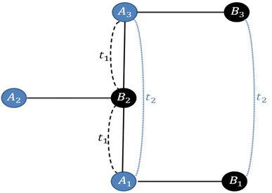 |
| | Fig. 1 Schematic diagram of ABA-trilayer graphene representing the relative position of sublattices Ai and Bi. t1 and t2 are the nearest and next nearest hopping parameters. | |
The tunable bandgap and high electronic properties of graphene such as the way the charge carriers respond to both external electric and magnetic fields offer great opportunities for scientists to design and develop highly efficient optical and electronic devices. To develop these interesting applications, which totally depend on their optical and electronic properties; a scheme of superlattice in graphene-based nanostructures has attracted a great deal of research interest in the last decade. Since, the work published by Esaki and Tsu in 1970 on semiconductor superlattices,28 nowadays, a great deal of attention has been devoted to graphene superlattices to study the electronic properties under periodic electric and magnetic potentials.29–41 In these studies, researchers have demonstrated effective band gap engineering and optical modulation by using external periodic potentials. Theoretically, it was predicted that the superlattice potential modifies the transport properties of graphene, which are completely different from superconductor superlattices.42 Periodic Kronig–Penny (KP) type of potential in single-layer graphene leads to the generation of extra Dirac points in the energy spectrum,30–32,43 a renormalization of charge carrier group velocity29 and the phenomena of super-collimation.29,44 In single-layer graphene, the application of periodic superlattice potential opens an energy gap in the energy spectrum but under certain conditions, this superlattice periodic potential creates extra Dirac points in the energy spectrum and also closes the energy gap.45 The same periodic superlattices potential when applied to bilayer graphene induces an energy gap and also generates both zero energy and finite energy Dirac points in the energy spectrum.41,46 The KP-type periodic superlattice potential in ABC- and ABA-trilayer graphene superlattice generate extra Dirac points in the energy spectrum, which depends on the barrier height of the periodic potential.35 The impact of KP-type magnetic potential on trilayer graphene superlattices has also been incorporated in different studies.39,47–49
In this paper, we have investigated the effect of both electric and magnetic vector potential on the low energy spectrum of ABA-trilayer graphene superlattice. We first applied the electric and vector potentials separately and observed the changes that occur in the energy spectrum. The application of vector potential is unique, which generates finite energy Dirac points due to the intersection of second and third mini-bands. These Dirac points are symmetric about ky = 0 line when the barrier and well widths of the vector potential are identical. However, for different barriers and well widths, the symmetry of the finite energy Dirac points about Fermi level get destroyed. The application of electric potential causes the generation of zero energy Dirac points in the energy spectrum. These Dirac points emerge both from the original Dirac point as well as from the valleys developed in the energy spectrum by increasing the barrier height of the electric potential. The application of both electric and vector potentials together changes the symmetry of the spectrum with respect to zero energy level and with respect to ky = 0 planes depending on layer potentials.
The paper is organized as follows: in Section 2 we have discussed the theoretical model of ABA-trilayer graphene superlattice Hamiltonian. We have also elaborated the periodic electric and magnetic superlattice potentials in Subsections 2.1 and 2.2, respectively. The problem has been further solved numerically and the numerical results have been discussed in Section 3 of the result and discussion section. Finally, we have concluded the paper in Section 4.
2. Formulism
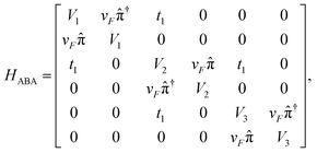
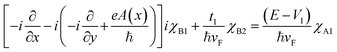
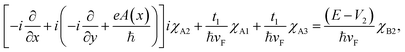
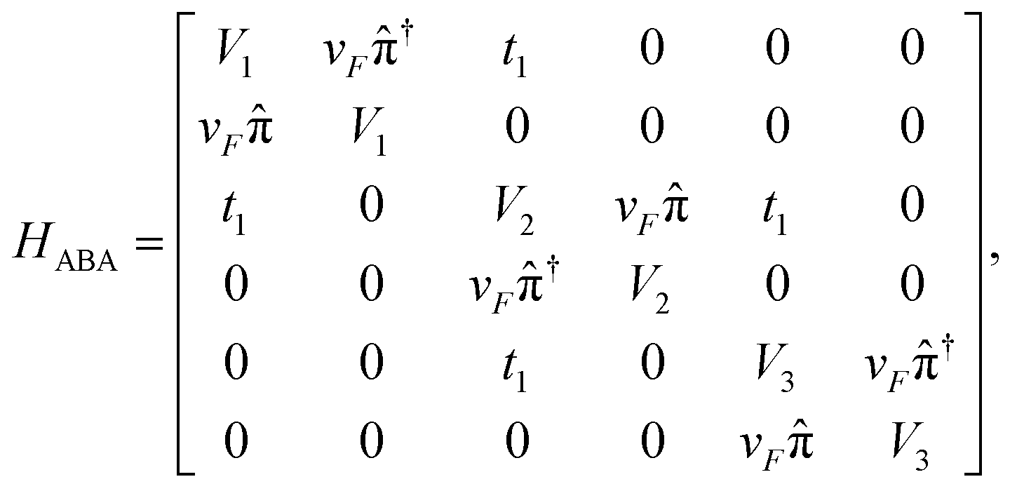
In order to study the band structure and electronic properties of ABA-trilayer graphene superlattice with Kronig-Penny type of electric and vector potentials, we have considered three coupled layers of graphene with ABA stacking order. In ABA-trilayer graphene, atoms of the top layer lie exactly on top of the bottom layer as shown in Fig. 1. The hopping strength between neighboring and next neighboring layers is represented by the coupling parameters t1 and t2, respectively, and the hopping strength between sites within each layer is represented by t. The low energy Hamiltonian of ABA-trilayer graphene with both electric and magnetic potentials is given by23| |
 | (1) |
where V1, V2, and V3 are the electric potentials in each layer respectively. ![[small pi, Greek, circumflex]](https://www.rsc.org/images/entities/char_e1de.gif) =
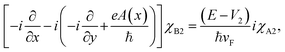
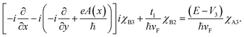
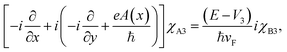
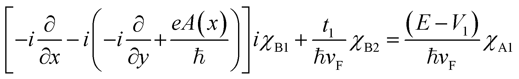
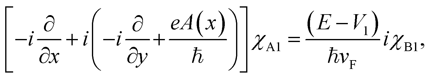
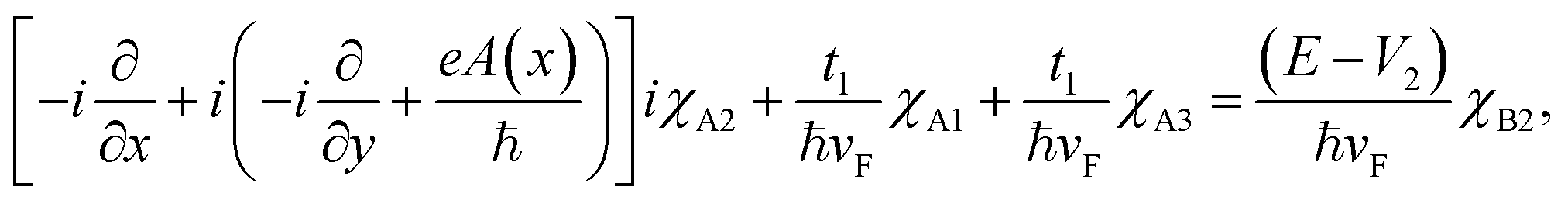
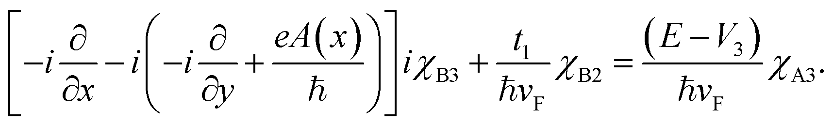
= ![[p with combining circumflex]](https://www.rsc.org/images/entities/i_char_0070_0302.gif) x + i(y + eA), where x and y are the components of the in-plane momentum operator, A is the vector potential, which is defined by the Landau gauge i.e., A(x) = (0, B0x, 0) with B0 a uniform magnetic field that is perpendicular to the superlattice plane. Next, we are going to diagonalize the above Hamiltonian, for which we define the eigenstate as χ = [χA1, iχB1, χB2, iχA2, χA3, iχB3]T with T denoting the transpose and the subscript representing the corresponding sublattices. Expanding the eigenvalue equation Hχ = Eχ, we get the following set of six equations.
x + i(y + eA), where x and y are the components of the in-plane momentum operator, A is the vector potential, which is defined by the Landau gauge i.e., A(x) = (0, B0x, 0) with B0 a uniform magnetic field that is perpendicular to the superlattice plane. Next, we are going to diagonalize the above Hamiltonian, for which we define the eigenstate as χ = [χA1, iχB1, χB2, iχA2, χA3, iχB3]T with T denoting the transpose and the subscript representing the corresponding sublattices. Expanding the eigenvalue equation Hχ = Eχ, we get the following set of six equations.| |
 | (2.1) |
| |
 | (2.2) |
| |
 | (2.3) |
| |
 | (2.4) |
| |
 | (2.5) |
| |
 | (2.6) |
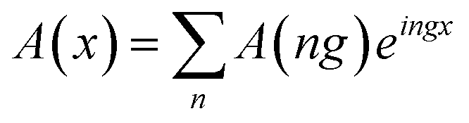
These equations are all written in the position space. To write these equations in momentum space, we use the Fourier transformation of the wavefunction and periodic electric and vector potential as
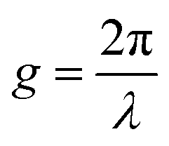
where = 0, ±1, ±2,… and

is the reciprocal lattice vector with
λ being the period of the periodic electric or vector potential. Using these transformations in the above equations and after a straightforward calculation we obtain the following modified equation in the momentum space.
| |
 | (3.1) |
| |
 | (3.2) |
| |
 | (3.3) |
| |
 | (3.5) |
| |
 | (3.4) |
| |
 | (3.6) |
The above six equations are written in dimensionless units. Here, we define the length unit as  , which is the magnetic length of the magnetic field. Using this length unit, the vector potential is expressed in the unit of B0lB, the electric potential V(x), the coupling parameter t1 and the energy E are written in units of
  and kx, ky, respectively, and the corresponding reciprocal lattice vector is expressed in units of 1/lB. The above sets of equations are six simultaneous equations that link
  with
with  for all possible values of m. Expanding all these equations and writing them in a matrix form, we finally obtain the following general form of superlattice Hamiltonian as
| |
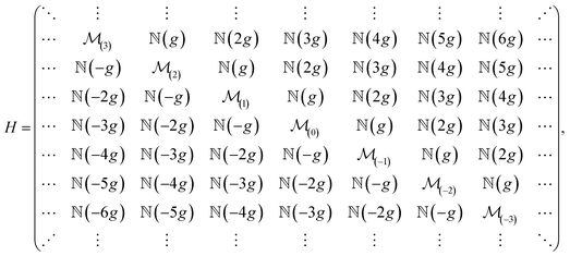 | (4) |
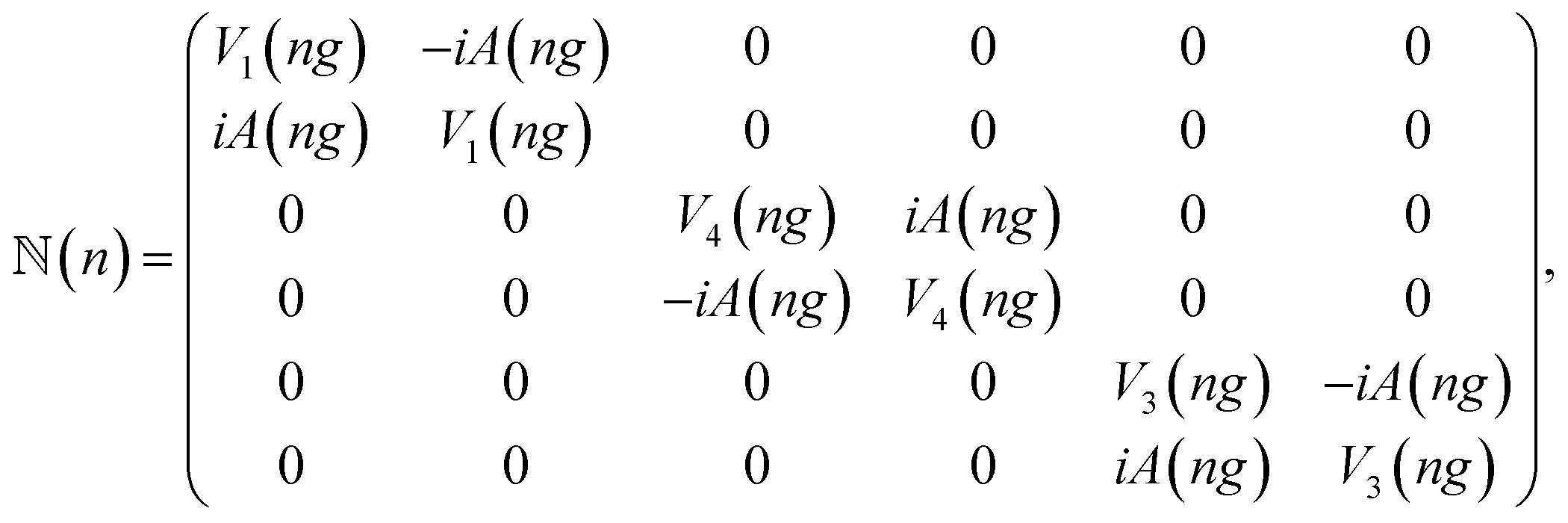
here the diagonal and off-diagonal matrices are defined as
| |
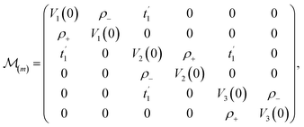 | (5) |
and
| |
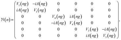 | (6) |
where
ρ± =
kx +
mg ±
i(
ky +
A(0)),
m = 0, ±1, ±2, … and
n = ±1, ±2, … We will solve
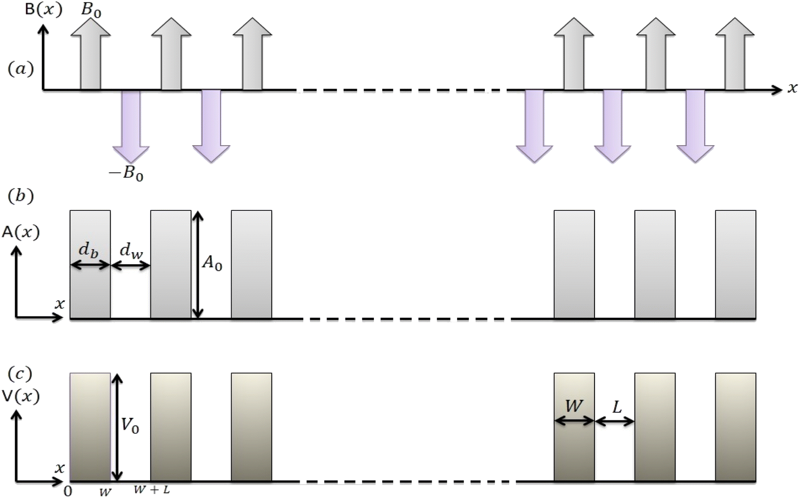
eqn (4) numerically and obtain the energy eigenvalues and corresponding energy spectra for different values of barrier heights of the electric and vector potentials, which we will discuss in detail in Section 3. We apply both periodic electric and vector potentials as shown in
Fig. 2.
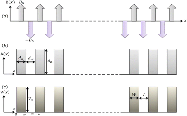 |
| | Fig. 2 Schematic diagram of superlattice potentials; (a) alternating magnetic strip with signs B0 and −B0 representing by up and down arrows respectively and (b) the corresponding Kronig-Penney type of vector potential A(x) with barrier width db, well width dw and strength (barrier height) A0. (c) Periodic Kronig–Penney type of electric potential V(x) with barrier width W, well width L and barrier height V0. Both potentials are zero inside the wells and non-zero inside the barriers. | |
2.1. Periodic Kronig–Penney type of superlattice vector potential
The applied magnetic field and the corresponding vector potential are shown in Fig. 2(a) and (b), respectively. The field is considered uniform along y-direction and staggered along the x-direction on a length scale that is greater than the lattice constant. The vector potential in the Landau gauge with barrier width db (Bz = B0) and well width dw (Bz = −B0) is characterized by the function| |
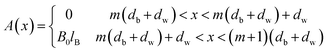 | (7) |
where m = 0, ±1, ±2, …, and λ = db + dw is the superlattice period. Since the vector potential is periodic with superlattice period d, it can be expanded using Fourier series as 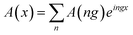 , where A(ng) is the Fourier coefficient and is given by
| |
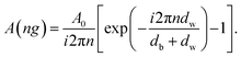 | (8) |
2.2. Periodic Kronig–Penney type of superlattice electric potential
The one-dimensional periodic electric potential V(x) is shown in Fig. 2(c), which is periodic along x-direction with period d = L + W, where W is the barrier width, L is the barrier separation and the height of the barrier is V0. This potential for convenience is modeled by the function| |
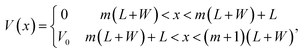 | (9) |
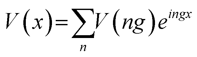
where m = 0, ±1, ±2, …, and λ = L + W is the superlattice period. Thus electric potential can be expanded in a Fourier series as 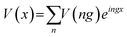 , where V(ng) is the Fourier coefficient given by
| |
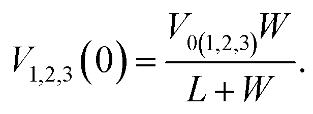
 | (10) |
where the subscripts 1, 2, 3 in V1,2,3(ng) represent the potential in each layer, respectively. Similarly| |
 | (11) |
3. Results and discussion
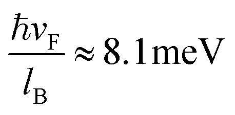
Before discussing the results, we define some of the parameters. The value of the magnetic field produced by the periodic magnetic strip in the barrier of width db can range up to 1T, having typical values of the order of a tenth of tesla. Thus, for B0 = 0.1T, the energy scales and magnetic length are  and lB = 80 nm, respectively, also t1 = 0.35 eV corresponds to
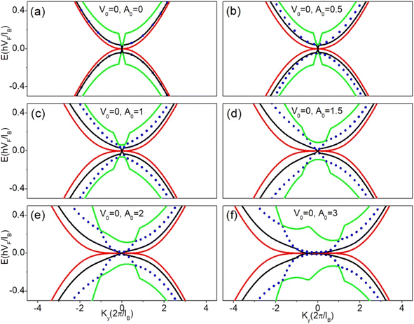
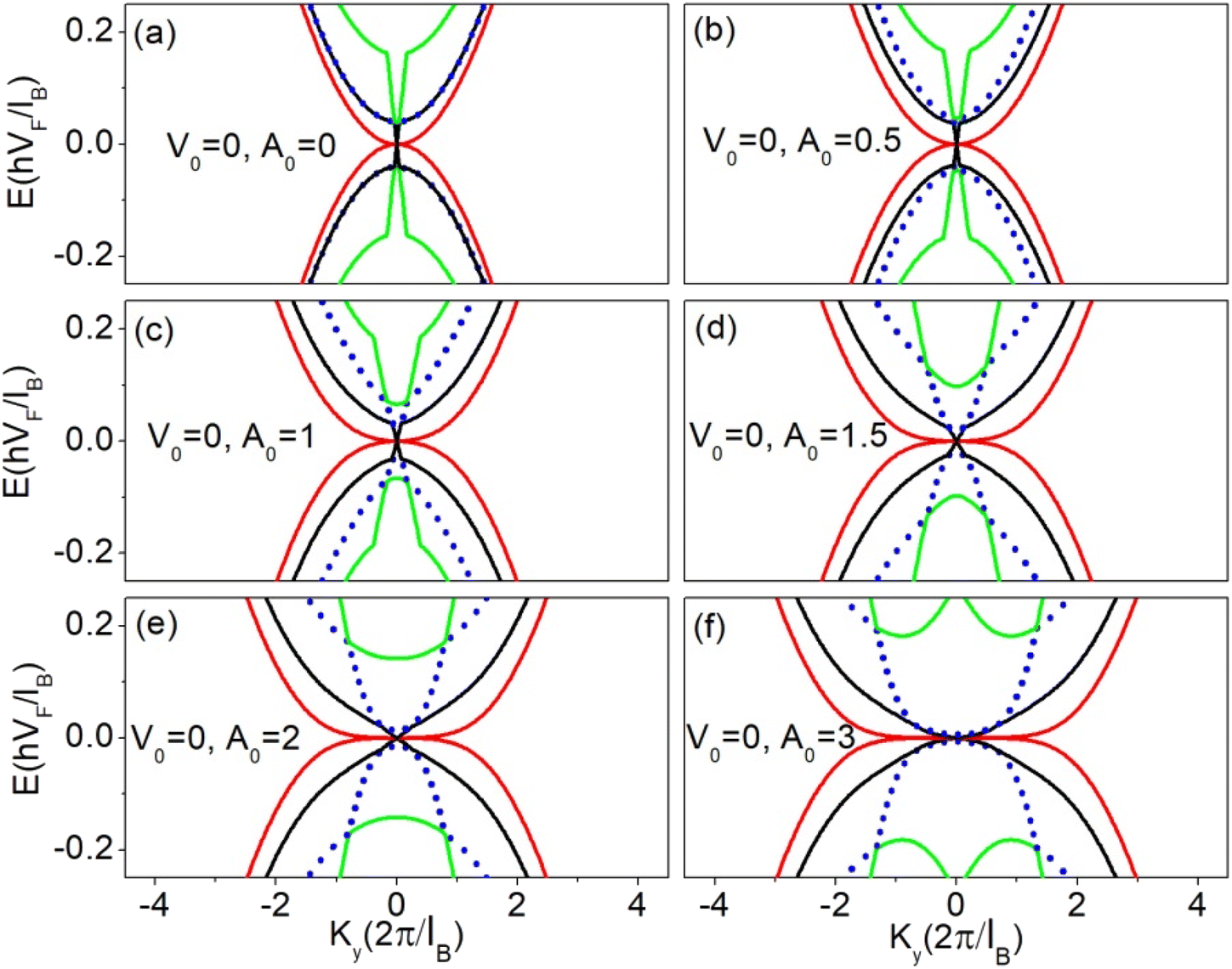
First, we will examine the full band structure of the ABA-trilayer graphene superlattice by applying the vector potential only and keeping the electric potential zero. The effect of different values of barrier height A0 of the vector potential on the low energy spectrum with identical barrier and well widths (db = dw = 5, d = 10) is shown in Fig. 3. To check the symmetry of the low energy spectrum with respect to the zero energy level, both positive and negative energy results are drawn here. When the barrier height of the vector potential A0 = 0, the dispersion relation is a combination of linear and quadratic dispersion close to ky = 0, shown in Fig. 3(a) by black and red curves, where the electron behaves in both massless and massive fermions, respectively.24,27 By increasing the barrier height A0 of the vector potential to 0.5, the linear and quadratic bands get more flatten while there is an emergence of second mini-band shown by blue dotted line in Fig. 3(b). This newly emerging mini-band touches the third mini-band (green curve) and generates two finite energy Dirac points on either side of ky = 0 when the barrier height is increased to 1.5, as shown in Fig. 3(d). Further, increase in barrier height of the vector potential does not generate any other extra Dirac points in the energy spectrum but only flattens the linear and quadratic bands and shifts the two Dirac points to higher energies as shown in Fig. 3(e) and (f). Both these Dirac points are symmetric about ky = 0 plane. Similarly, other mini-bands also intersect at higher energies and produce extra Dirac points on either side of ky = 0 with an increase in barrier height of the vector potential which is not shown in Fig. 3. The inclusion of the hopping term t2 in the low energy Hamiltonian of the ABA-trilayer graphene superlattice does not change the results significantly. The only difference observed due to the inclusion of t2 is that the emergence of extra Dirac points appears in the energy spectrum at slightly different potentials.
 |
| | Fig. 3 Energy dispersion along ky direction (kx = 0) for different values of barrier height A0 with identical barrier and well widths (db = dw = 5 and d = 10). The barrier heights A0 = 0, 0.5, 1, 1.5, 2, 3 in (a)–(f) respectively. | |
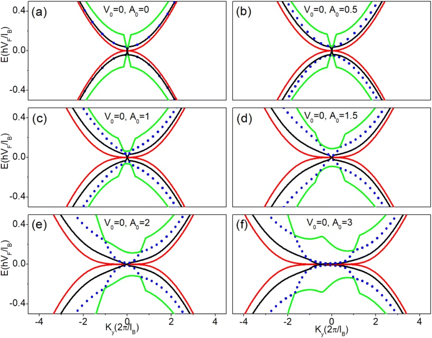
The dispersion relation for different values of barrier height A0 with unequal barriers and will widths, i.e., db = 4 and dw = 6 is depicted in Fig. 4. The energy dispersion of this asymmetric case (db ≠ dw) has different behavior as compared to the symmetric case (db = dw). At A0 = 1 (Fig. 4(c)) extra Dirac points emerge from the intersection of second and third mini-bands, these extra Dirac points are not symmetric about the ky = 0 plane. The distance of the left Dirac point from ky = 0 is comparatively large as compared to that on the right Dirac point. The left Dirac point is situated at higher energy as compared to the left Dirac point as shown in Fig. 4(d–f). The behavior of the quadratic dispersion remains the same while there is a slight shift in the linear dispersion. Thus, extra Dirac points show asymmetric behavior with respect to the ky = 0 plane and are located at different energies. Further, an increase in the barrier height does not create any other extra Dirac point but only causes a change in the curvature of the existing Dirac points and also increases the asymmetry in the energy dispersion.
 |
| | Fig. 4 Energy dispersion along ky direction (kx = 0) for different values of barrier height A0 with unequal barrier and well widths (db = 4, dw = 6 and d = 10). The barrier heights A0 = 0, 0.5, 1, 1.5, 2, 3 in (a)–(f) respectively. | |
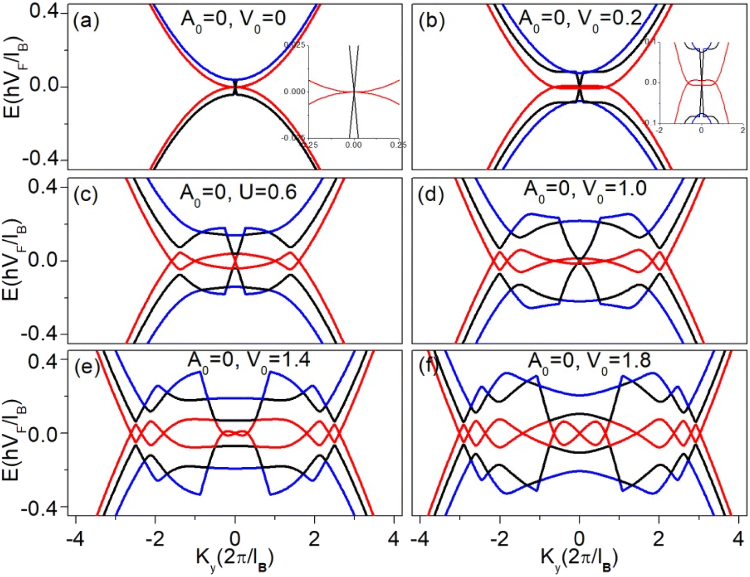
Next, we will consider the effect of periodic electric potential only and then we will explore the impact of both electric and vector potentials together on the low energy spectrum of the ABA-trilayer graphene superlattice. For the periodic electric potential, we consider two different cases; first by assuming that all the three layers of the ABA-trilayer graphene superlattice have the same potential i.e., V1(ng) = V2(ng) = V3(ng) = V(g) where  . Fig. 5 shows the dispersion relation along the ky direction for different values of the barrier height V0 of the electric potential while keeping the vector potential zero. When the barrier height of the electric potential is increased from 0, the quadratic dispersion becomes linear close to ky = 0, as a result, a Dirac cone appears in the middle and valleys also emerge in the spectrum. The valleys get closer with an increase in barrier height and finally touch each other when the barrier height reaches 0.2 as shown in Fig. 5(b). Two extra Dirac points appear in the energy spectrum due to the touching of the valleys, and at the same time, the central Dirac point is converted into a parabolic curve. Further, an increase in the barrier height causes the emergence of two extra Dirac points from the central Dirac point as shown in Fig. 5(c). The newly generated Dirac points move away from the original Dirac point along ky direction and at the same time the central Dirac point becomes parabolic, this parabolic dispersion close to ky = 0 generated two other extra Dirac points as we increased the barrier height, which is shown in Fig. 5(e and d).
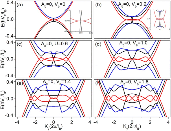 |
| | Fig. 5 Energy dispersion along ky direction for kx = 0 for the first three mini-bands, with equal barrier and well widths (L = W = 5) and different barrier heights V0 = 0, 0.2, 0.6, 1, 1.4, 1.8 in (a)–(f) respectively. | |
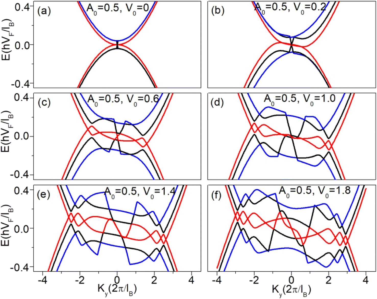
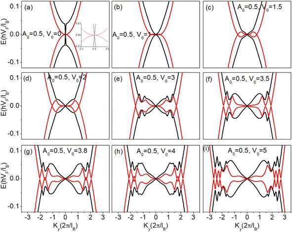
Now we discuss the combined effect of both electric and vector potential on the low energy spectrum of the ABA-trilayer graphene superlattice. We consider the case with all three layers having the same electric potential. Fig. 6 shows the E versus ky dispersion having identical barriers and well widths of both electric and vector potentials. The barrier height of the vector potential is kept constant (A0 = 0.5) while the barrier height of the electric potential varies, as shown in Fig. 6(a–f). Owing to the impact of periodic electric potential, extra Dirac points emerge in the energy spectrum by increasing the barrier height of the electric potential, which is discussed in detail in Fig. 5. The application of constant vector potential (A0 = 0.5) cannot produce any extra Dirac points but only breaks the symmetry of the spectrum about the Fermi level as shown in Fig. 6(a–f).
 |
| | Fig. 6 Energy dispersion along the ky direction (kx = 0) with equal barrier and well widths (db = dw = 5, L = W = 5, d = L + W = db + dw = 10). The barrier height of the vector potential is 0.5 which is constant while the barrier height of the electric potential is different. The barrier heights V0 = 0, 0.2, 0.6, 1.0, 1.4, 1.8 in (a)–(f) respectively. | |
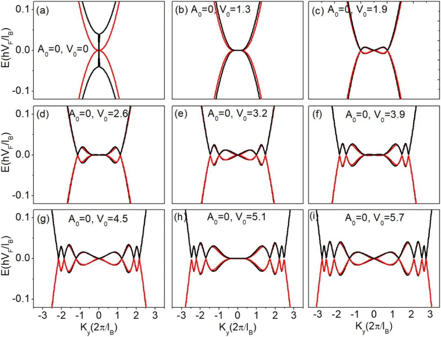
The effect of the electric potential while keeping the vector potential zero on the low energy dispersion of ABA-trilayer graphene superlattice is analyzed in Fig. 7, but this time all three layers are considered to be at different potentials. Such type of arrangement can be achieved by using two gate potentials with opposite polarities one at the top and the second at the bottom of the superlattice structure. The top gate has potential +V and the bottom gate has potential −V and if we ignore the screening, the three potentials would be V1(ng) = V(ng), V2(ng) = 0 and V3(ng) = −V(ng). When the barrier height of the electric potential is increased, the linear band gradually shifted to the nonlinear band (parabolic band). At barrier height V0 = 1.3, the two bands overlap each other close to ky = 0, as shown in Fig. 7(b) and become more flatten along the ky direction. A slight increase in the barrier height above V0 = 1.3 emerge two extra Dirac points in the energy spectrum having the same electron–hole crossing energy as that of the original Dirac point as shown in Fig. 7(c) for V0 = 1.9. These extra Dirac points, which are initially close to the ky = 0 line are now shifted away along the ky direction with increasing V0 as shown in Fig. 7(d) for V0 = 2.6. Further, increase in the barrier height above V0 = 2.6 generates two additional extra Dirac points in the energy spectrum as shown in Fig. 7(e) for V0 = 3.2. This process of emerging of extra Dirac points continues with the barrier height in a periodic manner, which can be seen in Fig. 7(f–i). From these observations, we reached the conclusion that the emergence of extra Dirac points is periodic; two extra Dirac points appear in the spectrum by increasing the barrier height of the electric potential by 1.3. Such type of behavior of emergence of extra Dirac points in a periodic manner was also observed earlier for single-layer graphene superlattice.30 Fig. 8 shows the E versus ky dispersion having identical barrier and well width of both electric and vector potentials but the three layers have different electric potentials. A constant vector potential (of barrier height A0 = 0.5) is applied to the system, while the electric potential has different values. The application of constant vector potential along with electric potential does not destroy the symmetry of the spectrum, unlike in the case when all three layers have the same electric potential. The addition of vector potential along with electric potential modifies the generation of extra Dirac points. The extra Dirac points are generated both from the original Dirac point as well as from the valleys developed in the dispersion as can be seen in Fig. 8(a–i).
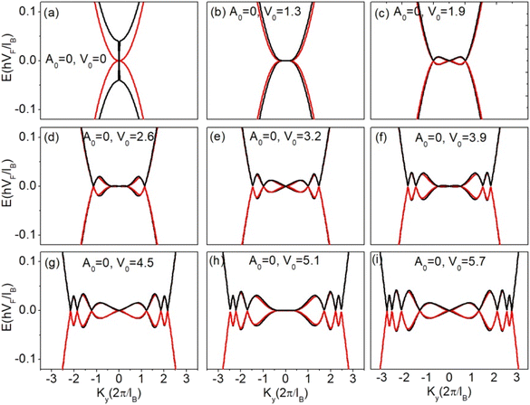 |
| | Fig. 7 Energy dispersion along ky direction for kx = 0, With different potentials for three layers. The barrier heights V0 = 0, 1.3, 1.9, 2.6, 3.2, 3.9, 4.5, 5.1, 5.7 in (a)–(i) respectively and the values of L and W are 5. | |
 |
| | Fig. 8 Energy dispersion along the ky direction (kx = 0) with same potential for each layer. The barrier and well widths are equal (db = dw = 5, L = W = 5, d = L + W = db + dw = 10), the barrier height of the vector potential is 0.5 which is constant while the barrier height of the electric potential V0 = 0, 1, 1.5, 2, 3, 3.5, 3.8, 4, 5 in (a)–(i) respectively. | |
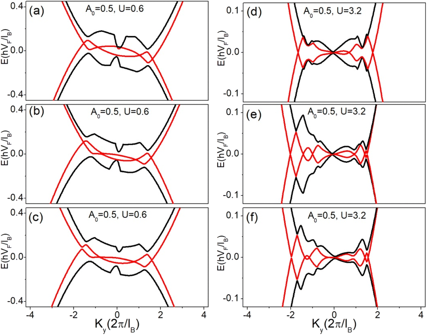
Finally, we discuss the asymmetric case for which the effect of both electric and vector potential is different as compared to the symmetric case. In Fig. 9(a–c) (left panel), the electric and vector potentials are the same (V0 = 0.6, A0 = 0.5), also all three layers have the same potential but have asymmetric barriers and well width. As shown in Fig. 9(a), the electric potential is symmetric (L = W = 5) while the vector potential is asymmetric (db = 6, dw = 4). This asymmetry of the vector potential not only destroys the symmetry of the spectrum but also annihilates the original Dirac points, the spectrum now twisted about the zero energy level. As shown in Fig. 9(b), the electric potential is asymmetric (L = 6, W = 4) and the vector potential is symmetric (db = dw = 5), again the asymmetry of the electric potential destroys both the symmetry of the spectrum as well as the initial Dirac points from the spectrum. For both electric and vector potentials to be asymmetric i.e., L = 6, W = 4, db = 6, dw = 4, the symmetry of the spectrum again destroys about the zero energy level, as shown in Fig. 9(c). Fig. 9(d–f) (right panel) shows the dispersion relation for the case where all three layers have different potentials with a constant barrier height of the electric and vector potentials i.e., A0 = 0.5 and V0 = 3.2 but different barriers and well widths. In Fig. 9(d), the electric potential is symmetric (L + W = 5) while the vector potential is asymmetric (db = 6, dw = 4), the energy spectrum now becomes asymmetric about ky = 0 line while the spectrum remains symmetric about the Fermi level. This asymmetry in the vector potential also destroys one of the Dirac points from the energy spectrum. Now, by making the electric potential asymmetric (L = 6, W = 4) and vector potential symmetric again the energy spectrum becomes asymmetric about the ky = 0 line and also generates extra Dirac points in the energy spectrum as shown in Fig. 9(e). By making both electric and vector potentials asymmetric i.e., L = 6, W = 4, db = 6, dw = 4, the symmetry of the spectrum again destroyed across the ky = 0 line and more and more extra Dirac points are generated in the energy spectrum.
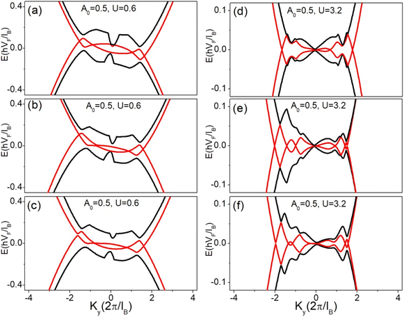 |
| | Fig. 9 Energy dispersion along the ky direction (kx = 0). The left panel is for the case when all the layers have the same potential and the right panel is for the case when all the three layers have different potentials. (a) L = W = 5, db = 6, dw = 4 with A0 = 0.5, V0 = 0.6 (b) L = 6, W = 4, db = dw = 5 with A0 = 0.5, V0 = 0.6 (c) L = 6, W = 4, db = 6, dw = 4 with A0 = 0.5, V0 = 0.6 (d) L = W = 5, db = 6, dw = 4 with A0 = 0.5, V0 = 3.2 (e) L = 6, W = 4, db = dw = 5 with A0 = 0.5, V0 = 3.2 and (f) L = 6, W = 4, db = 6, dw = 4 with A0 = 0.5, V0 = 3.6. | |
There has been a growing interest in the study of graphene superlattices in recent years because the study of superlattices provides a route to band structure engineering in semiconductor devices. The model and formulism provided in this work will be helpful in studying the electronic properties of a few (four and five) layers of graphene superlattices. These fascinating results will also be useful in analyzing the electronic properties while designing electric and magnetic field-effected trilayer graphene devices.
4. Conclusion
The effect of both electric and magnetic potential on the low energy spectrum of the ABA-trilayer graphene superlattice was investigated. We found that the application of vector potential causes the emergence of two extra Dirac points from the intersection of two min-bands other than the linear and quadratic bands of ABA-trilayer graphene. These extra Dirac points are symmetric about the ky = 0 line for equal barrier and well widths. However, for unequal barriers and well widths the symmetry of the extra Dirac points is broken both in terms of energy and in terms of their position with respect to the ky = 0 plane. The application of an electric potential to the ABA-trilayer graphene superlattice, when all three layers have the same potential, generates extra Dirac points with the same electron–hole crossing energy as that of the original Dirac point. These extra Dirac points are not only generated from the original Dirac point but also emerge from the valleys developed in the energy spectrum of the ABA-trilayer graphene superlattice. When both electric and vector potential are applied with the same barrier and well widths, the symmetry of the spectrum breaks about the Fermi level. Thus, a constant vector potential cannot generate any extra Dirac points but only breaks the symmetry of the spectrum about the zero energy level. Next, we analyzed the effect of the electric potential on the low energy spectrum of ABA-trilayer graphene by assuming that all three layers have different potentials and observing the emergence of extra Dirac points from the original Dirac point in a periodic manner. Each time two Dirac points emerge by increasing the barrier height of the vector potential V0 by a factor of 1.3. The application of both electric and vector potential when all three layers have different electric potential does not change the symmetry of the spectrum about zero energy level but only helps in generating additional Dirac points both from the original Dirac point as well as from the valleys that appeared in the spectrum. Next, we study the effect of asymmetric electric and vector potential on the low energy spectrum of the ABA-trilayer graphene superlattice. When all the layers have the same potential and either electric or vector potentials are asymmetric or both become asymmetric, the energy spectrum becomes asymmetric about the zero energy level and also these asymmetries destroy the original Dirac point from the energy spectrum. Similarly, when all the layers have different potentials, then the asymmetry in one of the potentials or in both potentials also destroys the spectrum but this time about the ky = 0 plane. The asymmetries in these potentials for the above-mentioned case also generate extra Dirac points other than the initial Dirac points that appear in the spectrum. In conclusion, our results show that the superlattice electric and vector potentials are an effective means to produce interesting features in the energy spectrum of the ABA-trilayer graphene superlattice
Data availability
The datasets used and/or analysed during the current study are available from the corresponding author on reasonable request.
Conflicts of interest
The authors declare that they have no known competing financial interests or personal relationships that could have appeared to influence the work reported in this paper.
References
- K. S. Novoselov, et al., Two-dimensional gas of massless Dirac fermions in graphene, nature, 2005, 438(7065), 197–200 CrossRef CAS.
- Y. Zhang, et al., Experimental observation of the quantum Hall effect and Berry's phase in graphene, nature, 2005, 438(7065), 201–204 CrossRef CAS PubMed.
- K. S. Novoselov, et al., Electric field effect in atomically thin carbon films, science, 2004, 306(5696), 666–669 CrossRef CAS.
- Y. Zhang, et al., Landau-level splitting in graphene in high magnetic fields, Phys. Rev. Lett., 2006, 96(13), 136806 CrossRef CAS PubMed.
- M. I. Katsnelson, K. S. Novoselov and A. K. Geim, Chiral tunnelling and the Klein paradox in graphene, Nat. Phys., 2006, 2(9), 620–625 Search PubMed.
- J. M. Pereira Jr, et al., Confined states and direction-dependent transmission in graphene quantum wells, Phys. Rev. B, 2006, 74(4), 045424 CrossRef.
- V. Gusynin and S. Sharapov, Unconventional integer quantum Hall effect in graphene, Phys. Rev. Lett., 2005, 95(14), 146801 CrossRef CAS PubMed.
- K. S. Novoselov, et al., Unconventional quantum Hall effect and Berry's phase of 2π in bilayer graphene, Nat. Phys., 2006, 2(3), 177–180 Search PubMed.
- E. McCann and V. I. Fal’ko, Landau-level degeneracy and quantum Hall effect in a graphite bilayer, Phys. Rev. Lett., 2006, 96(8), 086805 CrossRef PubMed.
- C. Berger, et al., Electronic confinement and coherence in patterned epitaxial graphene, Science, 2006, 312(5777), 1191–1196 CrossRef CAS PubMed.
- F. Zhang, et al., Band structure of A B C-stacked graphene trilayers, Phys. Rev. B, 2010, 82(3), 035409 CrossRef.
- M. Craciun, et al., Trilayer graphene is a semimetal with a gate-tunable band overlap, Nat. Nanotechnol., 2009, 4(6), 383–388 CrossRef CAS.
- T. Taychatanapat, et al., Quantum Hall effect and Landau-level crossing of Dirac fermions in trilayer graphene, Nat. Phys., 2011, 7(8), 621–625 Search PubMed.
- M. Koshino, Interlayer screening effect in graphene multilayers with A B A and A B C stacking, Phys. Rev. B, 2010, 81(12), 125304 CrossRef.
- S. B. Kumar and J. Guo, Multilayer graphene under vertical electric field, Appl. Phys. Lett., 2011, 98(22), 222101 CrossRef.
- W. Bao, et al., Stacking-dependent band gap and quantum transport in trilayer graphene, Nat. Phys., 2011, 7(12), 948–952 Search PubMed.
- C. H. Lui, et al., Observation of an electrically tunable band gap in trilayer graphene, Nat. Phys., 2011, 7(12), 944–947 Search PubMed.
- H. Min and A. H. MacDonald, Chiral decomposition in the electronic structure of graphene multilayers, Phys. Rev. B, 2008, 77(15), 155416 CrossRef.
- B. Partoens and F. Peeters, Normal and Dirac fermions in graphene multilayers: Tight-binding description of the electronic structure, Phys. Rev. B, 2007, 75(19), 193402 CrossRef.
- M. Aoki and H. Amawashi, Dependence of band structures on stacking and field in layered graphene, Solid State Commun., 2007, 142(3), 123–127 CrossRef CAS.
- F. Guinea, A. C. Neto and N. Peres, Electronic states and Landau levels in graphene stacks, Phys. Rev. B, 2006, 73(24), 245426 CrossRef.
- S. Latil and L. Henrard, Charge carriers in few-layer graphene films, Phys. Rev. Lett., 2006, 97(3), 036803 CrossRef PubMed.
- S. Sena, et al., Landau levels in asymmetric graphene trilayers, Phys. Rev. B, 2011, 84(20), 205448 CrossRef.
- C. Lu, et al., Influence of an electric field on the optical properties of few-layer graphene with AB stacking, Phys. Rev. B, 2006, 73(14), 144427 CrossRef.
- B. Partoens and F. Peeters, From graphene to graphite: Electronic structure around the K point, Phys. Rev. B, 2006, 74(7), 075404 CrossRef.
- F. Guinea, Charge distribution and screening in layered graphene systems, Phys. Rev. B, 2007, 75(23), 235433 CrossRef.
- M. Koshino and E. McCann, Trigonal warping and Berry's phase
N π in ABC-stacked multilayer graphene, Phys. Rev. B, 2009, 80(16), 165409 CrossRef.
- L. Esaki and R. Tsu, Superlattice and negative differential conductivity in semiconductors, IBM J. Res. Dev., 1970, 14(1), 61–65 CAS.
- C.-H. Park, et al., Anisotropic behaviours of massless Dirac fermions in graphene under periodic potentials, Nat. Phys., 2008, 4(3), 213–217 Search PubMed.
- C.-H. Park, et al., Landau levels and quantum Hall effect in graphene superlattices, Phys. Rev. Lett., 2009, 103(4), 046808 CrossRef.
- L. Brey and H. Fertig, Emerging zero modes for graphene in a periodic potential, Phys. Rev. Lett., 2009, 103(4), 046809 CrossRef CAS PubMed.
- M. Barbier, P. Vasilopoulos and F. Peeters, Extra Dirac points in the energy spectrum for superlattices on single-layer graphene, Phys. Rev. B, 2010, 81(7), 075438 CrossRef.
- G. Maksimova, et al., Graphene superlattice with periodically modulated Dirac gap, Phys. Rev. B: Condens. Matter Mater. Phys., 2012, 86(20), 205422 CrossRef.
- Z. Wu, J. Li and K. S. Chan, Charge pumping in monolayer graphene driven by a series of time-periodic potentials, Phys. Lett. A, 2012, 376(12–13), 1159–1165 CrossRef CAS.
- S. Uddin and K. Chan, Band structure of ABC-trilayer graphene superlattice, J. Appl. Phys., 2014, 116(20), 203704 CrossRef.
- L. Dell'Anna and A. De Martino, Magnetic superlattice and finite-energy Dirac points in graphene, Phys. Rev. B, 2011, 83(15), 155449 CrossRef.
- V. Q. Le, C. H. Pham and V. L. Nguyen, Magnetic Kronig–Penney-type graphene superlattices: finite energy Dirac points with anisotropic velocity renormalization, J. Phys.: Condens. Matter, 2012, 24(34), 345502 CrossRef.
- L. Dell'Anna, et al., Using magnetic stripes to stabilize superfluidity in electron-hole double monolayer graphene, Phys. Rev. B, 2015, 92(22), 220502 CrossRef.
- S. Uddin and K. Chan, Electric and magnetic superlattices in trilayer graphene, Phys. E, 2016, 75, 56–65 CrossRef CAS.
- X. Li, Z. Wu and J. Liu, Rashba spin-orbit coupling in graphene monolayer coated by periodic magnetic stripes, Sci. Rep., 2017, 7(1), 6526 CrossRef.
- T. Ahmad, et al., Band structure and extra Dirac points in the energy spectrum of ABA-Trilayer graphene superlattice, Phys. E, 2023, 149, 115669 CrossRef CAS.
- P. Burset, et al., Transport in superlattices on single-layer graphene, Phys. Rev. B, 2011, 83(19), 195434 CrossRef.
- C. H. Pham, H. C. Nguyen and V. L. Nguyen, Massless Dirac fermions in a graphene superlattice: a T-matrix approach, J. Phys.: Condens. Matter, 2010, 22(42), 425501 CrossRef PubMed.
- C.-H. Park, et al., Electron beam supercollimation in graphene superlattices, Nano Lett., 2008, 8(9), 2920–2924 CrossRef CAS PubMed.
- J. R. Lima, Electronic structure of a graphene superlattice with massive Dirac fermions, J. Appl. Phys., 2015, 117(8), 084303 CrossRef.
- M. Killi, S. Wu and A. Paramekanti, Band structures of bilayer graphene superlattices, Phys. Rev. Lett., 2011, 107(8), 086801 CrossRef.
- S. Ghosh and S.-J. Manish, Phys. Cond. Matt., 2009, 21, 292204 CrossRef.
- M. R. Masir, P. Vasilopoulos and F. Peeters, Magnetic Kronig–Penney model for Dirac electrons in single-layer graphene, New J. Phys., 2009, 11(9), 095009 CrossRef.
- M. R. Masir, P. Vasilopoulos and F. Peeters, Kronig–Penney model of scalar and vector potentials in graphene, J. Phys.: Condens. Matter, 2010, 22(46), 465302 CrossRef.
|
| This journal is © The Royal Society of Chemistry 2024 |
Click here to see how this site uses Cookies. View our privacy policy here. 
 Open Access Article
 This Open Access Article is licensed under a Creative Commons Attribution-Non Commercial 3.0 Unported Licence
 a and
Won-Chun Oh
a and
Won-Chun Oh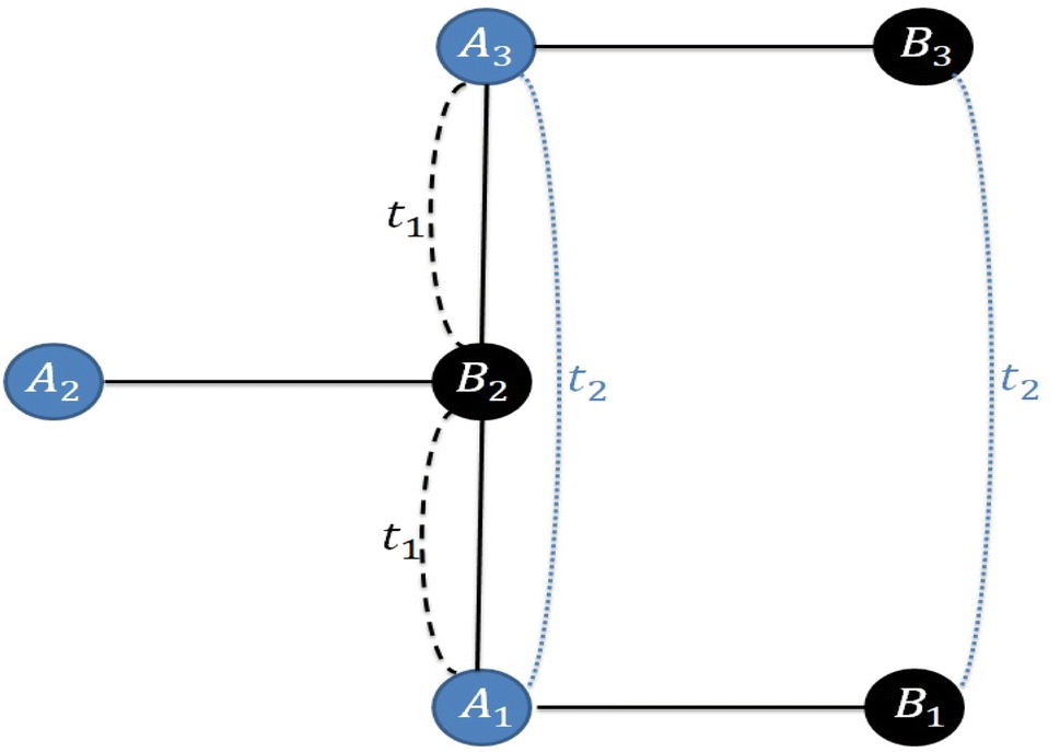


 is the reciprocal lattice vector with λ being the period of the periodic electric or vector potential. Using these transformations in the above equations and after a straightforward calculation we obtain the following modified equation in the momentum space.


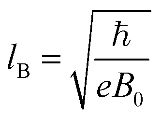 , which is the magnetic length of the magnetic field. Using this length unit, the vector potential is expressed in the unit of B0lB, the electric potential V(x), the coupling parameter t1 and the energy E are written in units of
 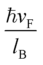 and kx, ky, respectively, and the corresponding reciprocal lattice vector is expressed in units of 1/lB. The above sets of equations are six simultaneous equations that link
  with
with 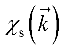 for all possible values of m. Expanding all these equations and writing them in a matrix form, we finally obtain the following general form of superlattice Hamiltonian as
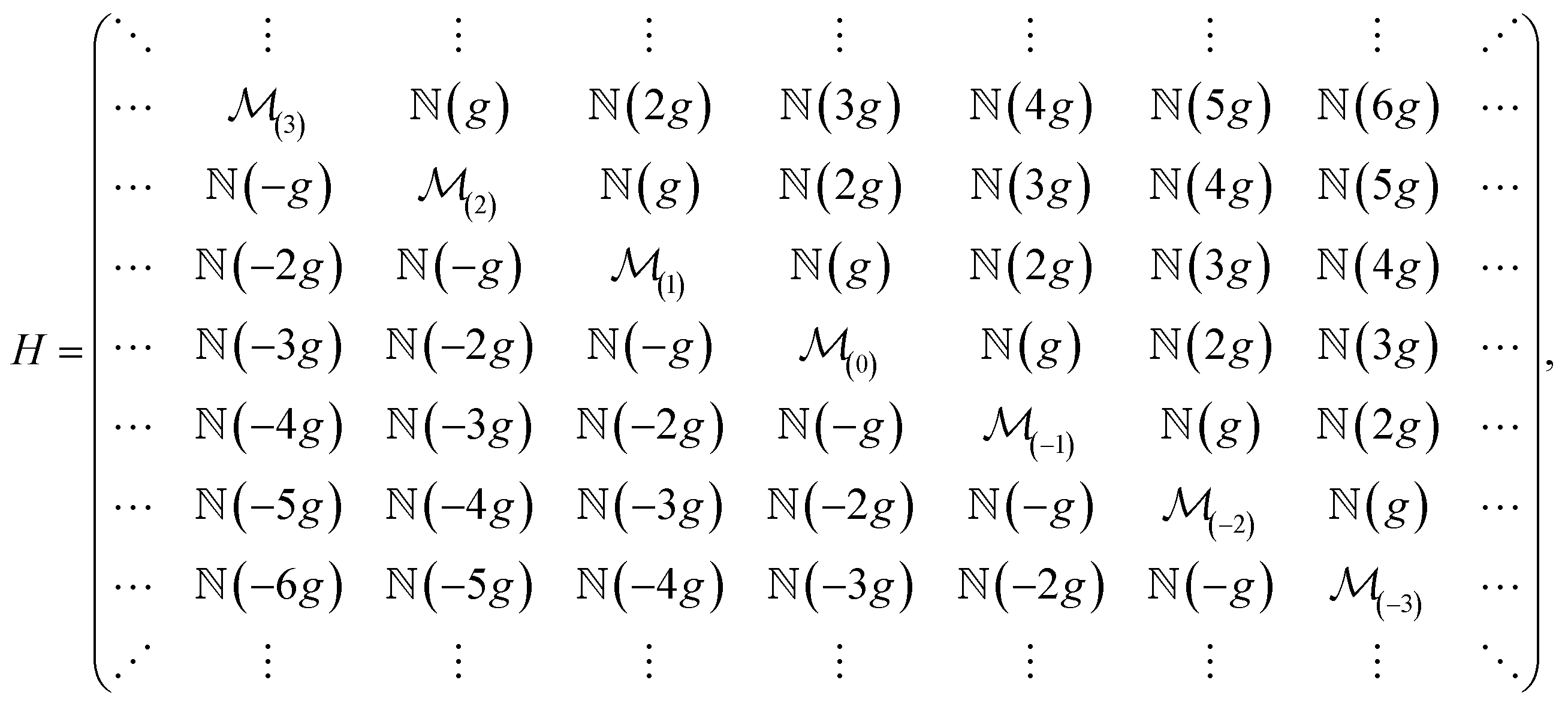

 , where A(ng) is the Fourier coefficient and is given by
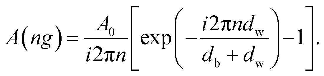

 , where V(ng) is the Fourier coefficient given by
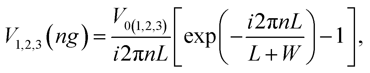
 and lB = 80 nm, respectively, also t1 = 0.35 eV corresponds to
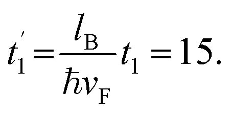
 . Fig. 5 shows the dispersion relation along the ky direction for different values of the barrier height V0 of the electric potential while keeping the vector potential zero. When the barrier height of the electric potential is increased from 0, the quadratic dispersion becomes linear close to ky = 0, as a result, a Dirac cone appears in the middle and valleys also emerge in the spectrum. The valleys get closer with an increase in barrier height and finally touch each other when the barrier height reaches 0.2 as shown in Fig. 5(b). Two extra Dirac points appear in the energy spectrum due to the touching of the valleys, and at the same time, the central Dirac point is converted into a parabolic curve. Further, an increase in the barrier height causes the emergence of two extra Dirac points from the central Dirac point as shown in Fig. 5(c). The newly generated Dirac points move away from the original Dirac point along ky direction and at the same time the central Dirac point becomes parabolic, this parabolic dispersion close to ky = 0 generated two other extra Dirac points as we increased the barrier height, which is shown in Fig. 5(e and d).