 Open Access Article
Creative Commons Attribution 3.0 Unported Licence
An insight in to microwave induced defects and its impact on nonlinear process in NiO nanostructures under femtosecond and continuous wave laser excitation
Ramseena Thundiyil a,
P. Poornesh
 *a,
K. Ozgab and
J. Jedrykab
aDepartment of Physics, Manipal Institute of Technology, Manipal Academy of Higher Education, Manipal, Karnataka 576104, India. E-mail: poornesh.p@manipal.edu; poorneshp@gmail.com
bFaculty of Electrical Engineering, Czestochowa University of Technology, Armii Krajowej 17, PL-42-201 Czestochowa, Poland
First published on 20th September 2024
Abstract
This work demonstrates the impact of microwave (MW) irradiation on third-order nonlinear optical (NLO) processes in chemically deposited NiO nanostructure films. The optical nonlinearity of the NiO nanostructure films was studied using third-harmonic generation (THG) measurements in the pulsed femtosecond laser regime and the Z-scan technique in the continuous wave laser regime. In the ultrafast pulsed regime, THG measurements revealed a significant increase in the THG signal of MW-irradiated NiO nanostructures due to photoexcitation and relaxation processes, resulting from an enhancement in defect concentration. This increase in defect density upon MW irradiation was quantified by PL and XPS studies. Under continuous wave laser irradiation, the Z-scan technique showed an enhanced absorption coefficient of ∼10−1 m W−1 and a nonlinear refractive index of ∼10−7 m2 W−1. The high NLO values in both pulsed and continuous laser regimes indicate that MW-irradiated NiO nanostructure films hold promise for optoelectronic device applications.
1. Introduction
Nanostructure films are pivotal in the realm of photonics due to their extensive range of optical applications. The nanoscale dimensions of these films significantly enhance their optoelectronic properties due to unique physical and optical characteristics at this scale. Nanomaterials exhibit size-dependent properties, including increased surface-to-volume ratios, quantum confinement effects, and enhanced light–matter interactions, thereby improving electron–photon interactions.1,2 These characteristics lead to improved performance in various promising fields, such as photonics, optoelectronics, telecommunications, biomedical optics, and nonlinear optics (NLO).In the field of NLO, researchers have extensively studied the effects of high-intensity light on nanomaterials.3–5 These studies have revealed the exceptional capabilities of nanomaterials for multiphoton absorption and high nonlinear absorption coefficients. These properties contribute to strong and swift responses in NLO materials, making them ideal for advanced applications. The nonlinear optical properties of metal oxides and doped metal oxide thin film nanoparticles have been rigorously investigated using various spectroscopic techniques.6–8 The unique NLO properties observed in these materials are being harnessed for applications in optical limiting, optoelectronics, telecommunications, and optical switching devices.9–11 NiO semiconductor stands out among various transparent metal oxides due to its wide bandgap and electronic, optical, and magnetic properties, making it valuable for interdisciplinary applications. Known for its high stability, both chemically and physically, as well as its low toxicity, and durability, NiO has a significant impact in various fields. In optoelectronics, NiO is recognized for its role in solar cells,12 photodetectors,13 and light-emitting diodes.14 When subjected to intense, coherent laser beams, NiO nanostructure films exhibit remarkable nonlinear optical properties.9,15
Post-deposition treatment techniques such as annealing and irradiation have been extensively studied for their ability to enhance the properties of NiO materials. High-energy beams with high-frequency irradiation, such as electron beams, gamma rays, and ultraviolet rays, are powerful tools for modifying the microstructural properties of materials. These beams have been extensively explored in various applications, particularly in the fields of electronics, sensing, and optoelectronics.16,17 They offer several advantages, such as the capacity to conveniently adjust the optical and structural properties of materials. Electron beams, gamma rays, and ultraviolet rays can induce significant changes in the properties of materials, making them highly desirable for a diverse array of applications. In addition to their utility in modifying the properties of materials, high-energy beams also offer several practical advantages. For instance, they can be precisely controlled to achieve the desired level of modification, allowing for fine-tuning of the material's properties. Numerous studies have reported that irradiation modifies the physical, chemical, and optical properties of NiO nanostructure films, leading to enhanced optical responses. In view of the mentioned distinctiveness of NiO films, many researchers have been attempting to explore their structural, optical, and NLO properties. M. Rashad et al.17 synthesized NiO nanoparticles via microwave irradiation and observed that UV exposure significantly reduces the optical bandgap by creating defects and disorders. They also noted that the nanoparticles exhibited enhanced optical nonlinearities associated with quantum size effects. P. Mallick et al.18 prepared NiO thin films on Si substrates using the electron vaporization method and subjected them to swift ion irradiation. The authors observed that swift ion irradiation improved the crystallization and texturing of the films at intermediate fluences, with changes in the crystallinity and texturing of NiO grains depending on the initial microstructure of the film. A. Qasem et al.19 investigated nanostructured NiO thin films treated with laser pulses ranging from 0 to 150, with intervals of 50 pulses. The energy band gaps were found to be lowered and the band tail energies to be extended upon exposure of laser light. SEM micrographs showed holes and cracks due to the laser breaking bonds between Ni2+ and O2− ions. The calculations confirmed the optical bandgap contraction and tail energy expansion with increasing pulses, attributed to increased defects. K. Jouini et al.20 prepared NiO thin films using spray pyrolysis and subjected them to gamma irradiation ranging from 180 Gy to 10 kGy. Structural studies revealed a phase transition from NiO to Ni2O3 beyond 5 kGy. At a 10 kGy dose, the films exhibited a combination of NiO and Ni2O3 phases, with optical studies showing activity in both the UV and visible ranges. This combination enhanced the photocatalytic performance under gamma ray treatment. Recent research has demonstrated that various irradiation methods can significantly modify the structural, optical, morphological, and nonlinear optical properties of NiO thin films. The findings from these studies confirm that irradiation enhances the material's properties.
Furthermore, these beams can be utilized across a diverse array of materials, establishing them as versatile tools in materials science and engineering. But sometimes, these high energy beams are found to destroy the materials also. This is where microwave (MW) irradiation, a low-frequency irradiation, offers a less destructive and more cost-effective approach to material modification. MW irradiation has emerged as a powerful tool in various fields due to its unique advantages over conventional heating methods.21 It offers several advantages over other forms of irradiation, such as rapid and uniform heating, higher yields, and reduced energy consumption.22 These benefits have led to its widespread adoption in research and industrial applications. Here, in this study, we are going to explore the new novelty field of the influence of MW irradiation on NiO nanostructure films. In this study, we need to emphasize the method that we employed to prepare for nanostructure NiO films. We utilized the air-assisted chemical spray pyrolysis method to prepare NiO nanostructured films. This method is renowned for its ability to produce uniform films and is favored for its simplicity and cost-effectiveness. Several deposition parameters include the flow rate of the spray, the amount of solution sprayed onto the substrate, the substrate temperature, and the distance between the nozzle and the substrate significantly influence the quality and uniformity of the nanostructure films. Optimizing these parameters is crucial for producing films, which attributes distinguish it from other deposition methods, making it a highly attractive option for the deposition of NiO nanostructure films.
The literature on third-order nonlinear optical effects in NiO nanostructures is limited. Additionally, comparative studies on the influence of NiO nanostructure films under continuous wave and pulsed laser regimes are not well-established. To address this gap, our recent study focused on synthesizing NiO nanostructure films using spray pyrolysis, followed by an extensive examination of their NLO response in NiO nanostructures using both CW and femtosecond pulsed lasers. Importantly, we aim to understand the NLO processes in systems treated with microwave irradiation and examine the impact of MW irradiation on both CW and pulsed laser regimes. Therefore, this research investigates the impact of microwave irradiation on the nonlinearity and thermo-optic properties of NiO nanostructure films, utilizing both pulsed and continuous wave laser regimes.
2. Experimental details
2.1. Materials used
Microscopic glass slides were acquired from Labtech. Acetone, 2-propanol (EMPLURA grade), and nickel acetate tetrahydrate (98% purity) were sourced from MERCK. Deionized water (18.3 MΩ) was used throughout all procedures. All chemical compounds were utilized to prepare the precursor solution for spray pyrolysis technique.2.2. Nanostructure thin film deposition
Microscopic glass slide substrates were cleaned sequentially with soapy water, deionized water, acetone, and isopropanol (IPA) for 10 minutes each using an ultrasonicate. Subsequently, the substrates were dried under a nitrogen flow. To ensure the removal of organic contaminants and reduce surface roughness, the substrates were then subjected to ozone treatment for 10 minutes, resulting in a cleaner and more uniform surface.The aqueous precursor solution was prepared by dissolving 1.2442 g of nickel acetate tetrahydrate (Ni(CH3COO)2·4H2O) in 100 mL of deionized water, followed by stirring for one hour to ensure a homogeneous and clear solution. This solution was then loaded into the spray pyrolysis syringe for direct use in NiO deposition. The substrate temperature was maintained at a constant 450 °C during the deposition process. The spray pyrolysis software controlled the spray head's motion along both the x and y axes. The solution was sprayed onto the glass substrate placed on the substrate holder, where it underwent pyrolysis, forming a thin film. The spraying nozzle and the substrate were spaced 19 cm apart with a solution being sprayed flow rate of 2 mL min−1. Air served as the carrier gas at 1 mbar. With 2 mm intervals, the ultrasonic nozzle moved in an S-shaped pattern in the x and y axes, maintaining a steady speed of 30 mm s−1. During deposition, the temperature varied by ±10 °C around 450 °C.
The nickel acetate tetrahydrate precursor solution decomposed and pyrolyzed at 450 °C, resulting in solid nickel oxide, while carbon dioxide and water were released as gases.
| Ni(CH3COO)2·4H2O → NiO + CO2↑ + H2O↑ | (1) |
The resulting film is light brown in color. The thickness of the film was ascertained through the utilization of a stylus profilometer, the film thickness was determined to be ∼250 nm.
2.3. Microwave irradiation
The NiO nanostructure films were subjected to microwave irradiation using a commercially available microwave oven (LG, model number: MC2146BRT) operating at a frequency of 2.45 GHz. The samples were positioned at the center of the microwave chamber on a rotating table. The microwave power was fixed at 800 W for irradiation. The irradiation time varied between 2, 3, 4, 5, and 10 minutes respectively. After each irradiation, the sample was allowed to cool, and it was observed that the sample became darker grey as the irradiation increased. Fig. 1 illustrates the changes observed in NiO nanostructure films upon MW irradiation. The schematic representation of process flow for preparation of microwave irradiated NiO nanostructure films, depicted in Fig. 2.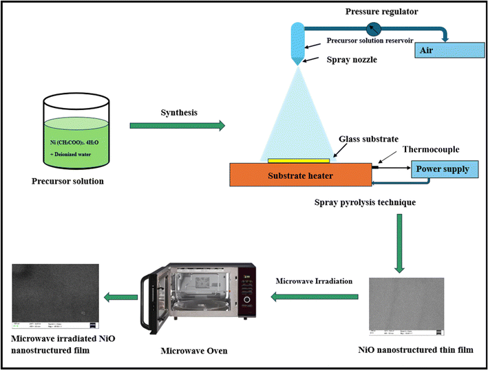 | ||
| Fig. 2 Schematic representation of process flow for preparation of microwave irradiated NiO nanostructure films. | ||
2.4. Characterization of nanostructure films
X-ray photoelectron spectroscopy (XPS) was utilized for the assessment of the oxidation state of the elements in the deposited films. The analysis was performed using an AXIS ULTRA system with a monochromatic Al Kα X-ray excitation source operating at 14 kV. The C 1s signal at 284.8 eV was used as the reference binding energy.
The nanostructure deposited films were analyzed for UV-visible light transmission using a 1900i UV-vis spectrophotometer, ranging from 190 to 1100 nm, with glass substrates providing the background. Photoluminescence studies were conducted to detect defects in the films, using a JASCO FP-8300 spectrofluorometer. Measurements were taken from 320 nm to 750 nm at ambient temperature, with an excitation wavelength of 300 nm, acquiring an emission spectrum for the thin films.
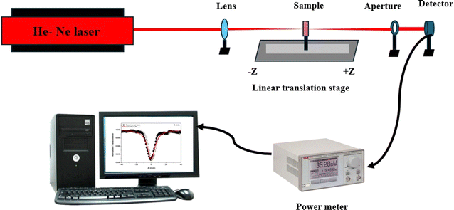
In this report, the NiO nanostructure film sample is irradiated by an intense continuous wave He–Ne laser with an input intensity of 20 mW. During the experiment, the beam is passed through a 5 cm convex lens, which focuses the beam on the sample. The obtained beam waist at the focal point and Rayleigh length were 35.11 μm and 6.11 mm, respectively. The thin film thickness meets the sample requirement L ≪ ZR, in which the Rayleigh range (ZR). The sample thickness is less than the Rayleigh length ZR, hence the thin film approximation is valid. Then, Z-scan experiments were conducted on the plane glass substrate, revealing no significant nonlinear contribution at the applied input power levels. Consequently, the glass substrate's impact on the observed nonlinearity was deemed negligible. A linear translation stage was employed to scan the NiO thin film in both positive and negative z-directions surrounding the convex lens's focal point. The scan range was ±5 cm. The laser power transmitted through the NiO film is utilized to measure both the nonlinear refractive index n2 and the nonlinear absorption coefficient β, with and without aperture, in front of the detector, accordingly. The detector is connected to power meters, utilized for measuring the laser power that passes through.
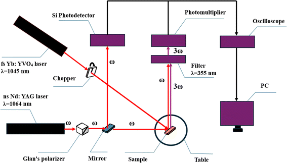
In this experiment, to determine the third harmonic signal of the material, we employed a femtosecond (fs) laser as the pumping laser. The fs laser used was a Yb:YVO4 laser with a wavelength of 1045 nm, a repetition frequency of 63 MHz, and a maximum energy of 40 nJ. This fs laser induces changes in the dipole moment of the sample, thereby altering the electronic states of the material. The high intensity and ultrashort pulses of the fs laser generate high peak powers necessary for strong nonlinear interactions. To prevent thermal damage to the samples due to prolonged exposure to the fs laser, a chopper was placed in the path of the laser beam. The chopper, with a single slit 2 mm wide, rotates at a speed of 1 revolution per second, effectively modulating the pulsed laser beam that falls on the sample. A nanosecond (ns) laser was also utilized, with its spot size corrected to approximately 1 mm to match that of the femtosecond laser, ensuring that both beams interact with the same area of the sample. This uniformity is crucial for consistent and reliable third harmonic generation (THG) measurements. The ns laser served as the probing laser beam, detecting changes induced by the pumping beam. The probing beam used was an Nd:YAG laser with a wavelength of 1064 nm, an 8 ns pulse duration, and a repetition frequency of 10 Hz. The laser beam had a diameter of 8 mm and a maximum energy of 150 J m−2.
The laser beam then passed through a Glan's polarizer placed in front of the beam path. The Glan polarizer ensured that the probing beam (from the ns laser) was highly polarized and allowed modulation of the light beam's intensity reaching the sample, leading to the tuning of the output fundamental energy density. The polarizer was capable of withstanding laser damage at 4 GW cm−2. We adjusted the polarizer angle in 5 degree increments to control the 1064 nm laser's energy reaching the NiO nanostructure film. This adjustment allowed us to detect the THG signal at the lowest possible energy density of the ns laser.
Following, the light passed through a transmissive mirror that reflected a portion of the incident light while transmitting the rest. This mirror directed part of the ns laser beam to a silicon photodetector (Si PD) and allowed another part to pass through to the sample surface. The reflective portion of the mirror directed a segment of the probing beam to the Si PD, used to synchronize the measurement system. The transmissive portion of the mirror allowed the probing beam to reach the sample surface, where it interacted with the changes in optical dipole moments induced by the fs pumping laser. The resulting THG signal then passed through an interference filter with a wavelength of 355 nm, which exclusively allowed the THG signal to pass through.
The THG signal was then recorded by a photomultiplier tube followed by an oscilloscope. The Tektronix MSO 3054 oscilloscope, with a high sampling rate of 2.5 GS s−1, provided high-resolution measurements of the fast-changing signals from the laser interactions, capturing both the fundamental signal (1064 nm) and the THG signal. The oscilloscope was connected to a PC for data acquisition and analysis. The whole experimental system was bounded in a box to eliminate the impact of external unwanted light dispersion, ensuring that the THG measurements reflected the true interactions within the sample, providing reliable and high-quality data.
3. Results and discussions
3.1. XRD analysis of MW irradiated NiO nanostructure films
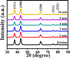
To investigate the crystal structure and phase of the prepared nanostructured films, structural studies were conducted using X-ray diffraction (XRD) analysis. The XRD patterns were obtained for both pristine and microwave irradiated NiO nanostructure films, as depicted in Fig. 5. The diffractograms reveal the presence of multiple peaks, indicating the polycrystalline nature of the films. All observed peaks correspond to the face-centered cubic structure of NiO, as indexed with the standard JCPDS file number 01-073-1519. The diffraction spectrum features three prominent peaks corresponding to the (111), (200), and (220) planes, along with two smaller peaks at the (311) and (222) planes. The polycrystallinity is evident in all samples. The preferential peak is towards the (200) plane, which is the most intense peak. Increasing the MW irradiation led to noticeable alterations in both peak intensity and full width at half-maximum (FWHM). Specifically, the intensity decreased with 5 minutes of MW irradiation but increased again for the 10 minute irradiated sample. These variations are attributed to the MW heating effect, which influences the orientation and arrangement of the lattice planes. Furthermore, the smaller plane peaks diminished with increased MW irradiation. The broadening of FWHM suggests an increase in strain within the film due to the MW heating effect. The observations, such as changes in intensity and FWHM, validate the structural alterations occurring in NiO thin films during MW exposure. These variations in intensity and FWHM may be attributed to the increased defect concentration resulting from dislocation or distortion within the film induced by irradiation.24A minimal peak shift (∼0.13°) towards lower angles was observed in samples irradiated for 2 to 10 minutes compared to the pristine samples, implying thermal expansion in the lattice parameters caused by MW heating. Furthermore, this alteration in the diffraction peak position is associated with changes in the local atomic environment of the Ni2+ ions within the crystal lattice. Such changes can be attributed to structural modifications, such as lattice distortion, strain,25 or the introduction of defects induced by MW irradiation. No additional peaks, which could indicate secondary phases or impurities, were detected after MW irradiation, confirming the purity of the samples. These findings demonstrate that MW irradiation affects the lattice atoms orientations and strain within the NiO thin films without introducing impurity phases.
The structural properties of the prepared nanostructured films, specifically the crystallite size and microstrain, were determined using two prominent analytical methods: the Scherrer method and the size–strain plot (SSP) method.
 | (2) |
 | (3) |
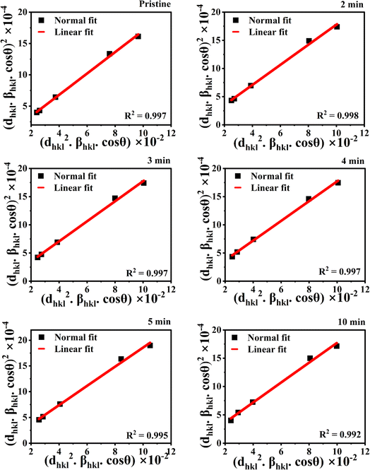
In the size–strain plot, (dhklβhkl![[thin space (1/6-em)]](https://www.rsc.org/images/entities/char_2009.gif) cos
cos![[thin space (1/6-em)]](https://www.rsc.org/images/entities/char_2009.gif) θ)2 is plotted on the Y-axis and (dhkl2βhkl
θ)2 is plotted on the Y-axis and (dhkl2βhkl![[thin space (1/6-em)]](https://www.rsc.org/images/entities/char_2009.gif) cos
cos![[thin space (1/6-em)]](https://www.rsc.org/images/entities/char_2009.gif) θ) on the X-axis, is depicted in Fig. 6. The slope of the plot provides the crystallite size, while the intercept gives the strain within the films. The SSP method focuses more on reflections at lower angles, where the accuracy and precision of XRD data are typically higher.
θ) on the X-axis, is depicted in Fig. 6. The slope of the plot provides the crystallite size, while the intercept gives the strain within the films. The SSP method focuses more on reflections at lower angles, where the accuracy and precision of XRD data are typically higher.
The crystallite sizes calculated using both the Scherrer method and the size–strain plot method are nearly equal, and both methods show consistent trends. The SSP method is more reliable and appropriate for analyzing the NiO nanostructure films because it minimizes the influence of less precise data and shows a good linear fit, indicating isotropic variations accurate in the crystallite size and strain of the NiO nanostructures upon MW irradiation. The crystallite size decreases with increasing microwave irradiation, from 8.24 nm to 7.47 nm according to the Scherrer method, and from 8.48 nm to 7.76 nm according to the SSP method. This reduction in crystallite size is attributed to the breaking up of crystallite size due to the MW heating effect. Irradiation can lead to the generation of heat in the material and influence the mobility of atoms in the crystal lattice, affecting the growth and stability of crystallites.26,27 Consequently, the irradiation period induces alterations in the film's microstructure by disrupting its original orderly arrangement.17
The dislocation density, which is a measure of point defects in the material, represents the number of dislocations per unit length and is calculated using the formula:
 | (4) |
After MW irradiation, the dislocation density of the film was found to increase, indicating that the levels of dislocation, distortion, and defects within the films have been enhanced. This increase is attributed to the MW heating effect, which induces more dislocations in the lattice.
The lattice parameter for the cubic structure is given by:
 | (5) |
Strain within the films was calculated using the equation:
 | (6) |
The films exhibit an increase in strain, which is associated with the elevated presence of defects induced by MW irradiation. However, a considerable difference in strain values was observed between the Scherrer and SSP methods. This indicates that the SSP method offers a more comprehensive analysis by considering strain. The number of crystallites per unit volume was determined using:
 | (7) |
The structural parameters values are depicted in Table 1 and it reveals that MW irradiation has been shown to increase dislocation density, induce strain, and enhance the number of crystallites in the films. These changes reflect significant modifications to the films' microstructure, which can influence their overall physical and chemical behavior.
| MW irradiation | Crystallite size (nm) | Dislocation density (×1016 lines per m2) | Strain (×10−2) | Number of crystallites per unit volume N (×1017 m−2) | Lattice constant a (Å) | ||||
|---|---|---|---|---|---|---|---|---|---|
| Scherrer | SSP | Scherrer | SSP | Scherrer | SSP | Scherrer | SSP | ||
| Pristine | 8.24 ± 0.02 | 8.48 ± 0.02 | 1.47 | 1.39 | 1.19 | 0.35 | 4.47 | 4.09 | 4.16 |
| 2 min | 7.82 ± 0.02 | 8.12 ± 0.02 | 1.64 | 1.52 | 1.25 | 0.46 | 5.24 | 4.67 | 4.17 |
| 3 min | 7.86 ± 0.02 | 8.14 ± 0.02 | 1.62 | 1.51 | 1.25 | 0.45 | 5.14 | 4.63 | 4.17 |
| 4 min | 7.90 ± 0.02 | 8.27 ± 0.02 | 1.60 | 1.46 | 1.24 | 0.88 | 5.07 | 4.43 | 4.17 |
| 5 min | 7.47 ± 0.02 | 7.76 ± 0.02 | 1.79 | 1.66 | 1.31 | 0.57 | 6.00 | 5.34 | 4.17 |
| 10 min | 7.79 ± 0.02 | 8.24 ± 0.02 | 1.65 | 1.47 | 1.26 | 0.77 | 5.29 | 4.47 | 4.17 |
3.2. Raman analysis of MW irradiated NiO nanostructure films
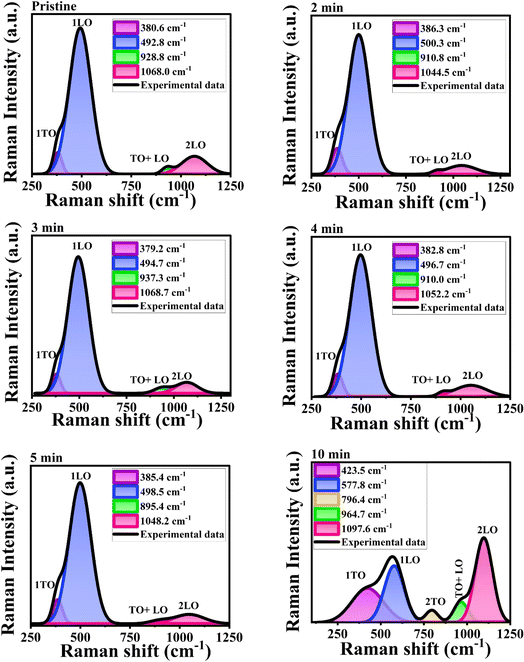
Raman spectroscopy was employed to investigate the vibrational modes and structural properties and to identify impurities in the films. This technique provides detailed information about the material's crystal structure and different vibrational modes. Fig. 7 illustrates the Gaussian deconvolution of Raman spectra of pristine and MW irradiated NiO nanostructure films, obtained using a 532 nm laser at room temperature over a scanning range from 200 to 1300 cm−1. The spectra, plotted as Raman intensity versus Raman shift, revealed the presence of five phonon modes characteristic of NiO films. These phonon modes include both first-order phonon modes (1TO and 1LO) and second-order phonon modes (2TO, LO + TO, and 2LO).The TO phonon modes exhibit a redshift from 380.6 to 423.5 cm−1 upon MW irradiation, with the FWHM increasing from 47 to 216 cm−1. The area of the TO mode is highest for the 2 minute irradiated sample, suggesting significant lattice distortion or the presence of nickel defect levels, corroborated by XRD spectra. The LO phonon modes shift from 492.8 to 577.8 cm−1, with an increased FWHM, attributed to the interaction of MW irradiation with NiO material. Similar observations have been reported by A. Sunny et al.31 The shifts observed in the TO and LO modes indicate the presence of vacancies and structural defects induced by MW irradiation.32 The movement of Raman peaks towards higher wavenumbers suggests an increase in defect concentration within the film after MW irradiation, possibly due to lattice defects introduced by the MW heating effect on the NiO structure.33
| MW irradiation | 1TO | 1LO | LO + TO | 2LO | ||||
|---|---|---|---|---|---|---|---|---|
| FWHM | Area | FWHM | Area | FWHM | Area | FWHM | Area | |
| Pristine | 47 ± 1 | 2038.9 ± 56 | 130.0 ± 0.4 | 37![[thin space (1/6-em)]](https://www.rsc.org/images/entities/char_2009.gif) 280 ± 92 280 ± 92 |
59 ± 5 | 687 ± 57 | 151 ± 61 | 5328 ± 95 |
| 2 min | 63.4 ± 0.7 | 10![[thin space (1/6-em)]](https://www.rsc.org/images/entities/char_2009.gif) 772 ± 148 772 ± 148 |
131.6 ± 0.2 | 120![[thin space (1/6-em)]](https://www.rsc.org/images/entities/char_2009.gif) 942 ± 1198 942 ± 1198 |
53 ± 6 | 802 ± 122 | 182 ± 1 4 | 10![[thin space (1/6-em)]](https://www.rsc.org/images/entities/char_2009.gif) 571 ± 228 571 ± 228 |
| 3 min | 51.2 ± 1 | 3207 ± 80 | 130.6 ± 0.3 | 58![[thin space (1/6-em)]](https://www.rsc.org/images/entities/char_2009.gif) 114 ± 112 114 ± 112 |
97 ± 7 | 1763 ± 169 | 134 ± 5 | 4815 ± 187 |
| 4 min | 57.8 ± 0.8 | 7341 ± 128 | 131.1 ± 0.2 | 104![[thin space (1/6-em)]](https://www.rsc.org/images/entities/char_2009.gif) 020 ± 192 020 ± 192 |
56 ± 5 | 1011 ± 123 | 191 ± 4 | 12![[thin space (1/6-em)]](https://www.rsc.org/images/entities/char_2009.gif) 285 ± 244 285 ± 244 |
| 5 min | 55.6 ± 0.7 | 7124 ± 102 | 130.0 ± 0.2 | 97![[thin space (1/6-em)]](https://www.rsc.org/images/entities/char_2009.gif) 519 ± 159 519 ± 159 |
115 ± 10 | 1790 ± 257 | 176 ± 5 | 8810 ± 293 |
| 10 min | 216 ± 6 | 7429 ± 27 | 134 ± 1 | 7639 ± 25 | 97 ± 3 | 2018 ± 73 | 118.9 ± 0.9 | 10![[thin space (1/6-em)]](https://www.rsc.org/images/entities/char_2009.gif) 052 ± 78 052 ± 78 |
In the pristine sample to the 5 minute MW-irradiated sample, the one-phonon 1LO mode exhibits higher intensity due to the presence of defects or surface defects. However, as the irradiation is extended to the 10 minute sample, the two-phonon LO band becomes more broadened compared to the 1P mode band. This increased broadening indicates higher disorder and defect levels within the nanostructure film. Additionally, the broad Raman signal supports the presence of oxygen vacancies and nickel-related defects.37 A similar behavior of the phonon-related Raman bands in nanosized material was observed in the study by Mironova et al.38 The shift of all Raman bands to higher wavenumbers indicates increased compressive strain in the films.39 Notably, the 10 minute sample shows significant peak shifts due to MW heating, with all phonon modes shifting to higher wavenumbers which is associated with the size-induced phonon confinement, defects, and surface relaxation.36 The shift in the 2LO peak from 1068 to 1097.6 cm−1 suggests the presence of crystal defects, such as oxygen and nickel vacancies, which can lead to a redshift of the Raman peak. Additionally, the modes broaden with increased MW irradiation due to higher nickel or interstitial oxygen vacancy concentrations, resulting in smaller particle sizes. Raman studies verifies that the prepared nanostructure films have a cubic NiO structure without any impurity or secondary phases, consistent with XRD results. In conclusion, these results imply that MW irradiation induces changes in the defect in the lattice of the material. This highlights the significant impact of MW irradiation on the material's crystallinity and defects.
3.3. XPS analysis of MW irradiated NiO nanostructure films
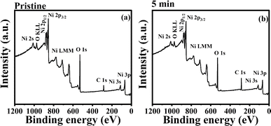
The chemical analysis of the sample was further carried out to determine the chemical state of the prepared NiO nanostructured NiO films. The XPS studies were conducted to analyze the chemical states and to identify the chemical compositions present in the prepared pristine and MW irradiated NiO nanostructure films. The Fig. 8 represents the XPS survey scan of the pristine and 5 min MW irradiated NiO nanostructure films.No foreign elements were detected in the wide spectrum, indicating the grown film has the desired NiO composition, consistent with XRD and Raman analyses. To account for the charging effect in the film on XPS, the binding energies were calibrated using the C 1s peak at 284.8 eV. The core spectra were plotted after correcting for the charging effect using this reference.
![[thin space (1/6-em)]](https://www.rsc.org/images/entities/char_2009.gif) :
:![[thin space (1/6-em)]](https://www.rsc.org/images/entities/char_2009.gif) 1 ratio, which is clearly visible in the survey spectra. This intensity ratio is determined by the number of electrons in each state, reflecting the degeneracy of the elements.
1 ratio, which is clearly visible in the survey spectra. This intensity ratio is determined by the number of electrons in each state, reflecting the degeneracy of the elements.
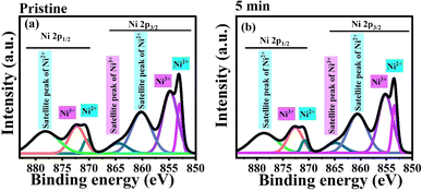
The binding energy of the Ni 2p3/2 component ranges from 850 to 868 eV, while the Ni 2p1/2 component ranges from 868 to 883 eV. In the Ni 2p3/2 region, four peaks are observed at 853.0, 854.8, 860.2, and 864.6 eV, corresponding to Ni2+, Ni3+, and the shake-up satellite peaks of Ni2+ and Ni3+, respectively, in the pristine NiO nanostructure film. The major peak at 853.0 eV and its satellite at 860.2 eV indicate Ni–O bonding in the Ni2+ state. The peaks at 854.8 eV and its satellite at 864.5 eV are associated with the Ni3+ state, indicating nickel vacancy defects in the film. For the Ni 2p1/2 region, binding energies from 868 to 883 eV are observed. Peaks at 870.4, 872.2, and 878.2 eV correspond to Ni2+, Ni3+, and the satellite peak of Ni2+, respectively. The occurrence of Ni2+ and Ni3+ states signify stoichiometric and non-stoichiometric NiO. Increased Ni 3d–O 2p hybridization and d–d transition mixing are the causes of the satellite peaks in the spectrum.40
In the 5 min MW irradiated sample, the Ni 2p3/2 binding energy peaks are observed at 854.4, 855.2, 860.6, and 864.9 eV. The Ni 2p1/2 binding energy peaks are observed at 870.8, 872.6, and 878.65 eV. After MW irradiation, the core spectra show a shift toward higher binding energies, which is attributed to the formation of defects in the NiO lattice. These defects alter the ionic charge distribution, leading to cation vacancies and changes in the chemical composition, particularly oxygen concentration.41 The peak broadening and shifts are also linked to the charging effect, which is induced by microwave irradiation.
The detailed analysis of the decomposed XPS spectrum indicates that the peak intensity for the core levels of Ni3+ (2p3/2 and 2p1/2) is higher than that for Ni2+ (2p3/2 and 2p1/2) in both pristine and 5 minute irradiated samples. The intensity ratio of Ni3+ to Ni2+ peaks (Ni3+/Ni2+) increases from 1.924 in the pristine sample to 2.029 in the irradiated sample, indicating a higher concentration of the Ni3+ state present in the film. The decrease in the intensity of the core levels for Ni2+ and Ni3+ is more noticeable in the 5 minute sample, suggesting the could be due to ionization effects caused by microwave irradiation, which leads to the ejection of electrons from the Ni2+ and Ni3+ states. Additionally, defects induced by irradiation can alter the local environment around the nickel ions, reducing the observable intensity of these peaks. Furthermore, the binding energy difference (ΔE) between the Ni 2p3/2 and Ni 2p1/2 peaks is 17.4 eV for both the pristine and 5 minute samples. This confirms that nickel is present in its oxidized forms (Ni2+ and Ni3+).
Overall, the XPS investigation confirms that non-stoichiometric NiO has a higher proportion of Ni3+ in both the pristine and 5 minute samples. This analysis supports PL analysis, which also showed an increase in the Ni3+ state after irradiation. Therefore, it can be concluded that the film contains different states of nickel, with a higher concentration of the Ni3+ state in the nickel oxide film.
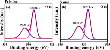
The deconvolution process revealed two predominant photoelectric emission bands of O 1s spectra. The pristine NiO thin films exhibit two distinct peaks located at 528.84 eV and 530.76 eV in the XPS spectra. The peak at the lower binding energy (528.84 eV) is attributed to lattice oxygen (OL) within the NiO matrix. This specific peak signifies the presence of oxygen atoms bonded with Ni2+ ions, forming the Ni–O octahedral coordination characteristic of the cubic rock salt structure.42 The presence of this peak indicates the stoichiometry of the NiO lattice,43 consistent with the XRD results.
The peak at the higher binding energy (530.76 eV) is associated with oxygen vacancies (OV) within the film.44,45 According to U. Kwon et al.,46 the presence of a peak around 531 eV can be attributed to a deficiency of Ni3+ ions and an excess of oxygen from NiO–OH. Similarly, research by Kotta et al.47 and R. S. Kate et al.48 supports this interpretation. M. Adak et al. also suggest that this peak corresponds to Ni3+ states in Ni2O3. The presence of oxygen vacancies has been confirmed by XPS analysis and is corroborated by results from PL spectra.
For the 5 min MW irradiated NiO film, the O 1s spectra exhibit peaks at 529.12 eV and 531.08 eV, respectively. These peaks indicate a shift towards higher binding energies compared to the pristine film. This shift, known as a chemical shift, reflects the alterations in the chemical states of the film induced by MW irradiation. The higher binding energy peaks suggest changes in the oxidation state and bonding environment of the oxygen atoms within the NiO lattice, highlighting the significant effect of MW irradiation on the film's chemical composition.
The area ratio of the oxygen 1s spectra for each peak was calculated, and it indicates that the percentage area of the lattice oxygen peak (OL) decreased from 61.7% to 54.1% upon MW irradiation. Conversely, the peak associated with oxygen vacancies increased from 38.3% to 45.9%. This change endorses the fact that MW irradiation enhanced the oxygen vacancy defects in the nanostructures, which is consistent with the PL analysis results.
3.4. FESEM and EDS analysis of MW irradiated NiO nanostructure films
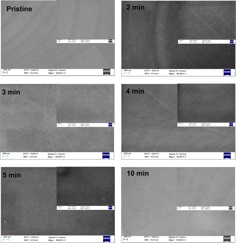
The morphology of the nanostructure films was analyzed using FESEM, which examined the surface morphology of both pristine and MW-irradiated NiO nanostructure films, as shown in Fig. 11. All prepared films exhibited smooth, uniform, crack-free surfaces with nanosized grains and distinct boundaries. MW irradiation resulted in relatively smaller and smoother nanograins compared to the pristine films, indicating that MW irradiation affects the grain size. The reduction in grain size upon irradiation may be associated with increased lattice strain, which restricts lattice growth. This irradiation induces changes in the film's microstructure, leading to a more dispersed system.EDS analysis was used to ascertain the elemental composition of NiO nanostructure films. In Table 3, EDS results for both pristine and MW-irradiated films indicate the exclusive occurrence of nickel (Ni) and oxygen (O) elements. With increased MW irradiation, the intensity of the O peak rises, indicating an increase in oxygen content in the films. Specifically, samples irradiated for 2 and 4 minutes show the highest oxygen peak intensity, likely due to a higher concentration of defect centers. This excess oxygen may result from the formation of Ni3+, which requires additional oxygen for charge compensation.49 Notably, XRD analysis did not detect any Ni2O3 phase in these films.50
| MW irradiation | Ni wt% | O wt% | Ni at% | O at% |
|---|---|---|---|---|
| Pristine | 67.76 | 32.24 | 36.42 | 63.58 |
| 2 min | 52.88 | 47.12 | 23.42 | 76.58 |
| 3 min | 67.07 | 32.93 | 35.69 | 64.31 |
| 4 min | 56.97 | 43.03 | 26.51 | 73.49 |
| 5 min | 60.19 | 39.81 | 29.18 | 70.82 |
| 10 min | 68.92 | 31.08 | 37.67 | 62.33 |
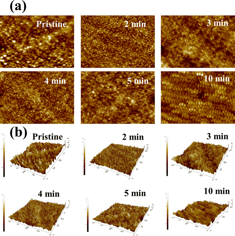
3.5 . AFM analysis of MW irradiated NiO nanostructure films
The morphology of MW irradiated NiO thin films was examined using AFM techniques with tapping mode, and 2D and 3D images are presented in Fig. 12. The scan area of the film is 1 by 1 μm. The AFM analysis of NiO provides clear evidence of morphological changes in the film, including alterations in grain sizes, ordered arrangement, and film roughness after irradiation. The observable change in grain size is evident from pristine to 2 min of MW irradiation. In the AFM image of the 2 min sample, grain is more fragmented into smaller entities and found to be a more ordered way of arrangement than the pristine film. The morphology of the 3 min samples exhibits a cluster of grains, while the 4 min irradiation results in a distinct formation of well-defined grains. In the case of 5 minutes, a reduction in grain size is observed along with the formation of clustered grains. The 10 min irradiation sample showed an increase in the grain size, attributed to the attributed to the impact of irradiation. This implies that MW irradiation induces modifications in the grain distribution within the NiO film.Variations in surface roughness were observed with increased MW irradiation. The surface roughness of the films is influenced by their crystallinity and texture; larger crystallite sizes generally result in smoother surfaces due to tighter packing of well-shaped grains. Table 4 shows the surface roughness values of the MW irradiated films. Values of roughness increased for the 2 minute irradiated sample, likely due to the presence of more dislocations and defects introduced by MW heating. However, with further irradiation, the roughness decreased, resulting in smoother surfaces due to reduced grain size and surface diffusion processes.51
| MW irradiation | Rq (nm) |
|---|---|
| Pure NiO | 1.091 |
| 2 min | 1.645 |
| 3 min | 1.176 |
| 4 min | 1.058 |
| 5 min | 1.083 |
| 10 min | 1.076 |
3.6. UV-visible analysis of MW irradiated NiO nanostructure films
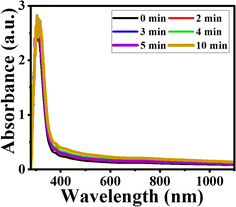
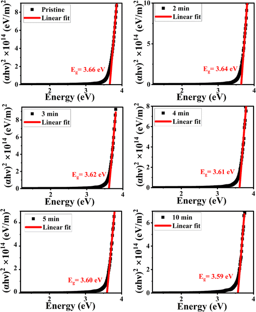
The optical properties of the materials, including absorbance and energy bandgap, were assessed using a UV-visible spectrophotometer at ambient temperature. Fig. 13 shows the absorption spectra of both pristine and MW-irradiated NiO nanostructure films, with an inset providing a detailed view of the irradiation effects on NiO. High absorbance is noted in the UV range of 300–320 nm, whereas the visible and IR regions exhibit low absorbance. The high absorbance in the UV region is attributed to the bandgap absorption of NiO.52 V. Usha et al.4 suggest that a UV region broad peak is associated with π–π* inter-band transitions. S. Ghazal53 suggests that the occurrence of this high band is due to transition of the O 2p band to the Ni 3d state of the CB. The absorbance edge for NiO is around 348 nm, shifting to 356 nm after 10 minutes of irradiation, indicating a redshift associated with bandgap shrinkage. This redshift is associated with the increased presence of defect centers and heightened scattering losses from grain boundaries, ultimately leading to an enhancement in absorption. Additionally, absorbance increases upon irradiation, with the 10 minute sample showing high absorbance at 318 nm. This enhancement is likely due to the increased optical scattering loss of light from the grain boundaries. The increased absorption can also be seen in Fig. 1, likely caused by the enhancement of defects such as oxygen vacancies and increased Ni3+ ion concentration.1,2 These defect states act as centers, contributing to greater light absorption within the material, resulting in increased absorbance as MW irradiation increases. Similar results have been reported in the literature.3According to structural investigations, irradiation enhances the defect densities in the lattice of the NiO nanostructure films. To confirm this change, we calculated the energy band gap of the pristine and MW-irradiated NiO nanostructure films, depicted in Fig. 14. The direct bandgap of the NiO films was determined utilizing Tauc's relation, given as:
| (αhν)2 = A(hν − Eg) | (8) |
| MW irradiation | Eg (eV) |
|---|---|
| Pristine | 3.66 |
| 2 min | 3.64 |
| 3 min | 3.62 |
| 4 min | 3.61 |
| 5 min | 3.60 |
| 10 min | 3.59 |
3.7. Photoluminescence analysis of MW irradiated NiO nanostructure films
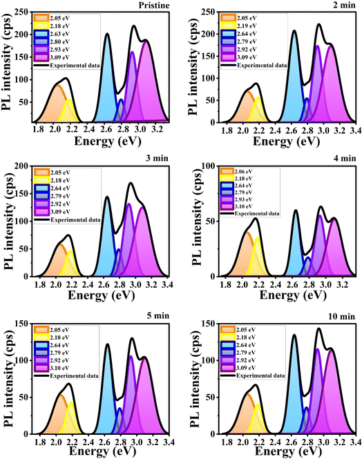
Photoluminescence (PL) spectroscopy provides critical insights into the crystal structure and defect densities within thin films. This technique is highly sensitive to defects, allowing for the detailed characterization of charge excitation and the electronic structure of the material. In our study, we investigated the PL spectra of pristine and microwave-irradiated NiO nanostructure films at room temperature, using an excitation wavelength of 300 nm.The PL spectra exhibited a wide range of emissions extending from ultraviolet (UV) to visible regions, indicating the presence of various defects in the NiO nanostructure films. UV emissions were associated with band-to-band transitions, while the broad and intense visible emissions were attributed to deep-level intrinsic emissions, including nickel and oxygen interstitials and vacancies.
To precisely determine the luminescent emission centers corresponding to these defects, we performed a deconvolution of the PL spectra using a Gaussian distribution function. The results of this deconvolution are illustrated by the solid black line in Fig. 15. The fitted parameters obtained from this analysis are summarized in Table 6, providing detailed information on the specific defect states contributing to the observed PL emissions.
| MW irradiation | UV | Violet | Blue I | Blue II | Yellow | Orange | |
|---|---|---|---|---|---|---|---|
| Pristine | Intensity | 189 | 161 | 56 | 201 | 56 | 88 |
| Area | 47 | 22.6 | 5.7 | 31.5 | 7.7 | 23 | |
| FWHM | 0.24 | 0.13 | 0.10 | 0.15 | 0.13 | 0.25 | |
| 2 min | Intensity | 174 | 170 | 57 | 208 | 59 | 70 |
| Area | 43.8 | 25.4 | 5.46 | 35.2 | 8.11 | 16.1 | |
| FWHM | 0.24 | 0.14 | 0.09 | 0.16 | 0.13 | 0.22 | |
| 3 min | Intensity | 125 | 132 | 49 | 143 | 46 | 57 |
| Area | 33 | 22.4 | 5.26 | 23.8 | 6.56 | 14.5 | |
| FWHM | 0.244 | 0.16 | 0.10 | 0.15 | 0.13 | 0.13 | |
| 4 min | Intensity | 52 | 55 | 17 | 60 | 35 | 40 |
| Area | 11.4 | 8.19 | 2.00 | 7.78 | 4.84 | 9.2 | |
| FWHM | 0.20 | 0.14 | 0.11 | 0.122 | 0.13 | 0.22 | |
| 5 min | Intensity | 103 | 106 | 35 | 122 | 43 | 53 |
| Area | 25.7 | 15.7 | 3.75 | 18.8 | 6.2 | 13.02 | |
| FWHM | 0.23 | 0.014 | 0.10 | 0.014 | 0.013 | 0.22 | |
| 10 min | Intensity | 115 | 115 | 36 | 135 | 40 | 55 |
| Area | 28.3 | 17.6 | 3.78 | 21.1 | 5.59 | 13.3 | |
| FWHM | 0.23 | 0.14 | 0.09 | 0.15 | 0.13 | 0.23 |
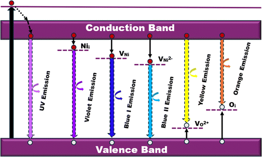
The PL spectra of pristine and MW-irradiated NiO nanostructures exhibit two prominent emission bands: one in the ultraviolet (UV) emission and another due to deep-level intrinsic emissions. The UV emission, corresponding to an energy of 3.09 eV, is accredited to near-band edge (NBE) excitonic recombination. The visible emission band, spanning from 2.93 to 2.05 eV, is associated with intrinsic defect levels caused by diverse structural defects, including oxygen vacancies and interstitial defects in the NiO films. Strong UV emissions arise from direct excitonic recombination near the band edge. F. Chandoul et al.55 suggest that the origin of this UV emission may be from oxygen vacancies in the NiO samples. The visible deep-level emissions are attributed to point defects, such as vacancies and interstitials within the nanostructured films.56,57 All visible transitions fall within the energy bandgap of the films, as determined from the Tauc plot, confirming that these defects are trapped within the material's bandgap. The deep-level emissions include violet emissions, broad blue emissions (blue I and blue II), as well as yellow and orange emissions across all prepared thin films. Fig. 16 illustrates the PL emissions resulting from various defect levels and the band edge transitions in NiO, providing a detailed band diagram representation.
The broad visible deep-level emission centers in MW irradiated NiO nanostructure films can be classified into two major categories. The first category includes emissions ranging from violet to wide blue, which are attributed to nickel-related defects within the films. The second category encompasses broad yellow to orange emissions, associated with oxygen-related defects.58 The energy emissions from 2.93 eV to 2.63 eV are linked to nickel defects, such as interstitials and vacancies in NiO materials. Mochizuki et al. suggest that the emission bands below 3 eV are attributed to nickel-related vacancy defects and occur due to charge transfer between Ni2+ and Ni3+.59,60 The emission at 2.93 eV corresponds to interstitial defects, attributed to the transition of electrons from nickel interstitial sites to holes in the valence band.58 Violet emissions arise due to the presence of nickel interstitial sites and surface defects, correlating with defect density. Blue I (2.80 eV) and blue II (2.63 eV) emission centers correspond to vacancy defects of nickel ions. The 2.80 eV emission is indicative of singly ionized nickel vacancies,60,61 while the 2.63 eV emission is attributed to doubly ionized nickel vacancies.62 Both transitions occur from nickel vacancy defect states to the valence band. The broad yellow to orange emissions detected in all nanostructured films, occurring at 2.18 to 2.06 eV, respectively, are attributed to defect-related emissions arising from oxygen vacancies.63 The 2.18 eV emission, appearing yellow, is attributed to the transition of electrons from the electron donor level to the acceptor level of oxygen vacancies. On the other hand, the orange emission at 2.06 eV is caused by oxygen interstitials.64 Also, the visible emissions occurred in the film due to the presence of defects at the grain boundaries, caused by the presence of nickel vacancies or the oxygen interstitials at grain boundaries.60
The effect of microwave irradiation on the position and intensity of defect peaks is illustrated in Fig. 15. While the peak positions remain stable with increasing MW irradiation, the intensity decreases in irradiated samples. A noticeable decrease in the variation of defect peak intensities was observed in the irradiated samples. The increase in irradiation creates defects such as vacancies, interstitials, and other surface imperfections, disrupting the regular lattice structure. These defects serve as non-radiative centers, leading to a decrease in PL intensity by dissipating energy as heat rather than light. Excessive defects further quench PL by forming non-radiative recombination centers.65 Moreover, the PL intensity indicates the dependency of defect density in the film, resulting in the weak recombination of photogenerated charge carriers.
There are no substantial deviations in the FWHM of the PL emission bands, but the area of the bands decreases with irradiation. The smallest band area was observed in samples irradiated for 4 and 5 minutes, indicating a higher number of defects and a reduction in luminescent centers. Additionally, the relative intensity between NBE emission and deep-level emission bands remains largely unchanged with irradiation.
After irradiation, a significant decrease in intensity was observed. Samples irradiated for 4 minutes exhibited a 75.76% reduction in UV emission intensity. This reduction is attributed to the microwave irradiation enhancing non-radiative defect levels in the lattice. XRD and Raman spectroscopy studies also support the incorporation of non-radiative defect centers upon irradiation. Ni interstitials were found to increase with irradiation, particularly in the 4 minute samples, while doubly ionized Ni vacancies decreased. The area ratio of nickel defects indicated an enhancement in nickel interstitials, with the highest levels observed in the 4 minute irradiated samples. Changes in the yellow-orange emission were also noted, with a decrease in oxygen interstitials and an increase in oxygen vacancies upon irradiation, consistent with XPS results. The calculated area ratios showed that the 5 minute film had the highest area ratio of 32% for oxygen vacancies, indicating a significant increase in oxygen vacancy defects. The area ratio quantity of the Ni and O defects were tabulated in Table 7. MW irradiation results in the decrease of PL intensity for NiO nanostructures, indicating that irradiation can effectively influence luminescence behavior. The quenching of PL emission with increasing irradiation dosage is due to the enhanced incorporation of non-radiative defect centers.
3.8. Third-order nonlinear optical processes of MW irradiated NiO nanostructure films
The theoretical understanding of NLO phenomena involves the interaction of high-intensity light, such as a laser, with an NLO material. The intensity of the light depends nonlinearly on the electric field. Consequently, the linear refraction and absorption become nonlinear and rely on the light's intensity as it passes through the material. This relationship is given by:
| α(I) = α0 + βeffI | (9) |
| n(I) = n0 + n2I | (10) |
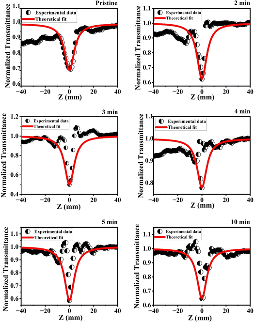
The NLA coefficient βeff of the material was determined using the OA Z-scan method, with an input intensity of 20 mW. The obtained results for the open-aperture Z-scan of the film, which correspond to the far-field normalized transmittance T(Z) as a function of the sample distance position from the beam focus, are shown in Fig. 17, represent the OA experimental data traces obtained with the Z-scan system. To obtain this graph, we used the general normalized transmittance equation for multiphoton absorption (MPA) in the OA Z-scan fit equation.
 | (11) |
 | (12) |
The open-aperture graph exhibits a dip at the focus, indicating positive nonlinear absorption characteristic of reverse saturable absorption (RSA).23 Microwave irradiation enhances the RSA nature, with the valley significantly deepening MW irradiation compared to the pristine sample, indicating an increased nonlinear absorption mechanism.
The occurrence of RSA can be attributed to several mechanisms, including two-photon absorption (TPA), multiphoton absorption (MPA), free-carrier absorption (FCA), excited state absorption (ESA), transient absorption, or a combination of these nonlinear absorption processes.66 These behaviors are closely related to the bandgap, defect densities, and free carriers present in the films. The continuous laser irradiation energy of 1.96 eV on the nanostructured films excites electrons from the valence band to the conduction band through defect levels in the films, leading to thermal induced excited state absorption. The enhanced and induced defect levels in the films observed due to MW irradiation are associated with increased nonlinear absorption. In these nanostructures, electrons excited from the ground state to defect levels through photon absorption emit non-radiatively. These trapped electrons can further absorb additional photons, causing excitation to the conduction band, facilitated by ESA. Additionally, the laser irradiation energy of 1.96 eV is insufficient to excite electrons from the valence band to the conduction band through single-photon absorption. The bandgap of the material is ∼3.6 eV, and since the laser photon energy is greater than half but less than the bandgap energy, TPA is possible. The laser energy of 1.96 eV fulfills the TPA condition. FCA also plays a crucial role in the nonlinear absorption mechanisms. Microwave irradiation enhances the generation of free carriers within the material, thereby promoting FCA. Despite being a relatively weak nonlinear absorption process, FCA contributes significantly alongside TPA.67 Although TPA and the FCA-induced TPA are allowed, the high observed absorptive nonlinearity indicates that the RSA is primarily due to thermally induced ESA. Therefore, the RSA process primarily stems from ESA and FCA induced by TPA.
The nonlinear absorption results from the combined contributions of multiple processes, denoted by βeff. The presence and enhancement of defect levels in the films observed with MW irradiation, identified through structural and spectroscopic studies, provide additional levels in the bandgap, which enhance the ESA mechanism, leading to RSA in the film.
After MW irradiation of the NiO nanostructured film, the RSA behavior was found to be enhanced. Using the NLA data, we determined the nonlinear absorption coefficient, which is presented in Table 8. The increase in the NLA coefficient after irradiation underscores the significant impact of MW irradiation on the material. This enhancement is attributed to the increased defect levels, including structural imperfections, oxygen, and Ni3+ defects, which promote excited state absorption along with single, two, three, or multiphoton absorption, leading to NLA processes.68 Additionally, FCA further amplifies these mechanisms.69 The enhanced NLA after irradiation suggests that MW treatment effectively improves the material's nonlinearity.
| MW irradiation | βeff × 10−1 (m W−1) | γ × 10−7 (m2 W−1) | n2 (esu) ×10−1 | Real χ3 × 10⁻² (esu) | Im χ3 × 10⁻³ (esu) | χ3 × 10⁻² (esu) |
|---|---|---|---|---|---|---|
| Pristine | 3.57 | 0.83 | 4.94 | 1.64 | 3.56 | 1.68 |
| 2 min | 4.85 | 1.31 | 8.44 | 3.24 | 6.04 | 3.30 |
| 3 min | 6.47 | 1.33 | 8.71 | 3.45 | 8.42 | 3.55 |
| 4 min | 2.93 | 0.94 | 6.71 | 3.20 | 5.05 | 3.24 |
| 5 min | 5.39 | 1.76 | 11.8 | 4.95 | 7.65 | 5.01 |
| 10 min | 4.76 | 1.11 | 8.22 | 4.22 | 9.15 | 4.32 |
These results indicate that the enhanced MW irradiation in NiO nanostructures leads to a greater NLA coefficient. It implies that the nonlinear absorption depends on the defect states induced by the irradiation, contributing to NLA and causing stronger NLA behavior in the MW-irradiated NiO nanostructured films. The results suggest that MW irradiation is suitable for enhancing the nonlinear optical absorption of NiO nanostructure films.
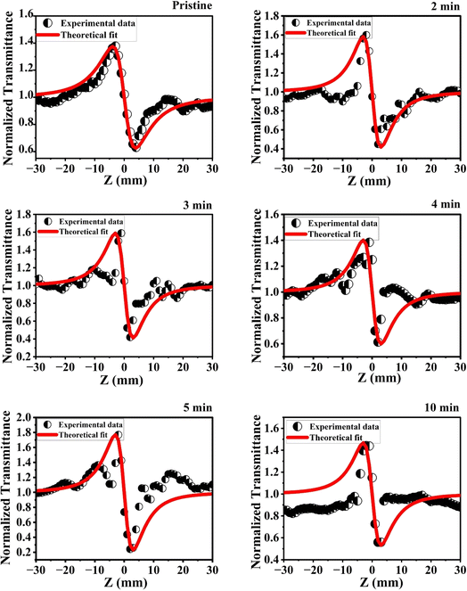
The samples showed a pre-focal peak and a post-focal valley signature, indicating negative nonlinear refractive behavior, demonstrating a self-defocusing effect indicative of induced thermal lensing effects. The transmittance for the closed-aperture (CA) Z-scan is given below:
 | (13) |
 Z is the sample position and ZR is the Rayleigh range. Δϕ is the on-axis nonlinear phase shift at focus. Normalized transmittance data is presented, with symbols representing the experimental data and solid lines depicting the theoretical transmittance fit to (5). Using the nonlinear refraction (NLR) plot of the material, we found the sign of the NLR indices to be negative. The nonlinear refractive index was calculated in both SI units and esu units, represented as γ (m2 W−1) and n2 (esu) respectively, and is given as follows:
 | (14) |
 | (15) |
The negative nonlinear refractive index in the samples is mainly caused by the thermal effects of the continuous wave laser. The CW laser irradiation on materials induces nonlocal thermal heating, which causes spatial variations in the refractive index of the material. These changes in the refractive index in the materials, which leads to materials to behave as a thermal lens due to the thermo-optic effect.71 The defect state levels in the MW irradiated NiO nanostructure films act as local thermal centers after absorbing incident photons and serve as centers for trapping excited electrons, enhancing non-radiative recombination. The non-uniform temperature distribution due to the irradiation causes variations in the refractive index of the MW irradiated material, which behaves like a defocusing lens, further leading to the enhancement in the negative nonlinear refractive index.
In the MW-irradiated NiO nanostructure film, peak-to-valley separation is greater than 1.7 times the ZR, strongly suggests that the nonlinearity predominantly arises from thermal effects.72 The nanomaterials exhibit absorption at the 633 nm wavelength, as seen in the absorption spectra. This absorption, combined with laser wavelength, leads to resonant nonlinearity, which further supports the presence of thermal nonlinearity in the material. Additionally, the CW laser typically enhances thermal nonlinearity through thermal lensing. Together, these factors confirm the dominance of thermal nonlinearity in this material.
Also, we employed the Z-scan technique to explore the effect of the glass substrate impacts the observed nonlinearity. Our results showed that the substrate did not exhibit any nonlinear optical effects, allowing us to eliminate the substrate's influence on our measurements.
In Fig. 17 and 18, we observe that the experimental Rayleigh length for MW-irradiated samples is narrower than the theoretical Rayleigh length. This is likely due to increased photon absorption processes, such as excited-state absorption (ESA), free-carrier absorption (FCA), and two-photon absorption (TPA). In this case, the nonlinearity is resonant, further amplifying these absorption processes. Additionally, the use of a CW laser contributes to thermo-optic nonlinearity, including thermal lensing, which plays a significant role in the increase in photon absorption.
The third-order susceptibility is a complex parameter that can be calculated using nonlinear optical parameters such as nonlinear absorption coefficient and nonlinear refractive index. The real part of the third-order susceptibility can be obtained from the nonlinear refractive indices, and it is given by:
| Real χ3 (m2 V−2) = 2n02ε0cγ (m2 W−1) | (16) |
With the nonlinear absorption coefficient, the imaginary component of the third-order susceptibility can be computed and expressed as follows:
 | (17) |
Then, the complex parameter third-order susceptibility can represent as,
 | (18) |
The below conversion relation helps in interchanging different units,
 | (19) |
The nonlinear optical parameters, including the nonlinear absorption coefficient (βeff), nonlinear refractive index (n2), and third-order susceptibilities (χ3), were calculated and summarized in Table 8. Microwave irradiation led to an increase in these parameters, such as NLA, which was attributed to induced electronic transitions and the creation of intermediate states in the films. The variations in the nonlinear refractive index observed are associated with local heating effects induced by the laser light.
An increase in the βeff observed with MW irradiation suggests that MW heating enhances the absorption nonlinearity of the NiO nanostructures. This enhancement is associated with the appearance of structural defects such as oxygen vacancies and Ni interstitials, which further lead to the enhancement of ESA, FCA, and TPA in the nanostructure. These enhancements result in the RSA mechanism being more pronounced, thereby increasing the NLA coefficient.
The higher values of the nonlinear refractive index and third-order susceptibility (χ(3)) observed with irradiation suggest the nanomaterial's potential for applications like optical limiting and optical storage. The third-order susceptibility (χ(3)) increased from 1.68 to 5.01 × 10⁻² esu, with the highest value observed for the 5 minute irradiated sample. This improvement is attributed to the reduced surface roughness, which minimizes light scattering and enhances the optical properties. Additionally, the increased number of defect center formations in the 5 minute samples enhances the NLO mechanisms. These enhanced defect densities in nanostructures findings align with previous analyses such as XRD, Raman, XPS, PL, and UV analysis. A comprehensive Table 9 that summarizes the recently reported NLO parameters for various doped and undoped NiO at CW laser. As far as we know, the current data demonstrates the highest nonlinear parameters for NiO films under continuous wave prepared using physical and chemical deposition methods to date. This indicates that MW irradiation is an efficient method to enhance the NLO properties of NiO, rendering it a highly suitable material for numerous NLO applications.
| Material | βeff (m W−1) | n2 (m2/W) | χ3 (esu) |
|---|---|---|---|
| Zn:NiO73 | 20.8 × 10⁻² to 25.3 × 10⁻² | 4.79 × 10⁻⁸ to 6.24 × 10⁻⁸ | 5.37 × 10⁻³ to 13.24 × 10⁻³ |
| NiO:Cr74 | 3.19 × 10⁻⁶ to 3.98 × 10⁻⁶ | 2.24 × 10⁻¹³ to 2.85 × 10⁻¹³ | 3.74 × 10⁻⁶ to 4.32 × 10⁻⁶ |
| NiO–Cu75 | 9.01 × 10⁻² to 9.81 × 10⁻² | 8.36 × 10⁻⁹ to 1.18 × 10⁻⁹ | 8.0 × 10⁻⁸ to 0.5 × 10⁻⁸ |
| NiO:Al76 | — | −8.67 × 10⁻⁹ to 11.67 × 10⁻⁹ | — |
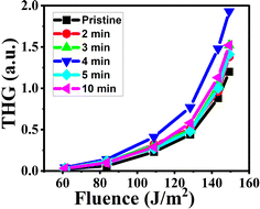 | ||
| Fig. 19 The illustration of THG signal with respect to the probing laser beam energy density of MW irradiated NiO nanostructure films. | ||
The THG signal varied with different probing laser beam energy densities from 60 to 150 J m−2. The plot reveals that there is no significant THG response for energy densities of the probing laser up to 60 J m−2. This suggests that below a certain threshold energy density, insufficient energy reaches the sample to generate a visible THG signal. However, as the energy density increases from 60 to 150 J m−2, there is a gradual enhancement in the THG signal. This enhancement is attributed to the interplay between photoexcitation and relaxation processes at localized trapping levels, a phenomenon also observed by other researchers77 with increasing power density.
For MW-irradiated NiO nanostructure films, the THG signal exhibits a non-monotonous trend. Initially, from pristine to 3 minute MW irradiation, the THG signal steadily increases. A significant enhancement is observed for the 4 minute irradiated films, followed by a decrease in THG for longer irradiation times. This behavior is explained by multiphoton excitation processes and optimized dipole moments, crystalline growth orientation, nanograin morphology, and optical properties.78 The enhanced THG signal for MW-irradiated films is attributed to increased optical absorption and excitonic effects. Enhanced optical absorption facilitates greater photon participation in the THG process, while excitonic effects contribute to photoexcitation and relaxation mechanisms. Overall, the interplay of these factors leads to the observed variations in the THG signal. The 4 minute MW-irradiated NiO sample shows a higher THG response than other samples, likely due to conditions favoring THG occurrence, increased photoexcitation and relaxation processes, and multiphoton absorption.79 This sample favors multiphoton excitation over third-harmonic processes, with interface trapping levels playing a significant role. Additionally, the 4 minute sample exhibits a low surface roughness value, contributing to the higher THG response.80 Furthermore, the laser-induced birefringence process substantially improves the THG signals through laser stimulation.79 These factors collectively contribute to the observed THG enhancement, attributed to improved photoexcitation and relaxation induced by the photo-induced pulsed laser. Non-regular increases in THG were observed by Upadhya et al.81 spray pyrolyzed Mg-doped ZnO films, where the enhancement in THG was attributed to the dipole moment of the excited states in the material. Albin et al.82 studied electron beam-irradiated GaZnO films under nanosecond and femtosecond laser regimes. They found significant results for both laser treatments, with enhancement in the femtosecond regime attributed to localized defects and laser-induced refractive index changes. In contrast, the enhancement in the nanosecond regime was primarily due to intra-energy gap states contributing to the NLO mechanisms. Essalah et al.79 reported a THG experiment with Nb2O5 and observed an increase in THG with rising Nb2O5 content. This enhancement was due to variations in atomic dipole moments, driven by mechanisms such as defect states, multiphoton processes, and additional photo polarization effects that alter the dipole moment of the atoms. Chattopadhyay et al.83 prepared Ce-doped ZnO via the coprecipitation method and found that the THG signal was enhanced when the dopant was in the interstitial position, while the THG signal decreased when the dopant substituted the ZnO nanoparticles. These findings align with the role of defect states in the observed variations in THG across different materials. Over 400 spots on the sample's surface were averaged in the results. After a few milliseconds, the photoinduced THG signal disappeared, demonstrating complete reversibility.84 Only when the photoinduced beam and the fundamental beam overlapped in both space and time was the THG signal recognized.
Results from THG and Z-scan measurements reveal variations in nonlinearity origins due to the distinct influences of femtosecond pulsed and CW laser excitations. The femtosecond pulsed regime enhances the nonlinear optical response through ultrafast electronic excitations, making MW-irradiated NiO films suitable for frequency conversion in high-power laser sources. The CW laser regime's nonlinearity, driven by thermal effects, can be applied in optical limiting materials. These studies show that MW irradiation substantially enhances the nonlinear optical parameters of NiO nanostructure films, compared to recent data in the thermal nonlinear domain. This confirms MW irradiation as a direct strategy to control and manipulate the nonlinear optical properties of NiO films. The interplay of ultrafast electronic contributions from the pulsed regime and thermal effects from the CW regime suggests that MW-irradiated NiO nanostructures are promising materials for current nonlinear optical applications.
4. Conclusion
The pristine and MW-irradiated NiO nanostructure films with a face-centered cubic structure were synthesized using the chemical spray pyrolysis method. The XRD analysis reveals that crystallite size decreased upon MW irradiation, from 8.26 nm to 7.74 nm, due to the MW heating phenomenon. Raman spectra confirmed the characteristic NiO phonon modes for MW-irradiated NiO films, with a red shift towards higher wavenumbers and increasing intensity for the MW-irradiated samples, indicating increased strain and defect density within the nanostructures. The oxidation states of the NiO were quantified using XPS studies. FE-SEM images confirmed that the nanostructures have a smooth surface with nanograin-like structures. AFM studies showed that variations in surface roughness upon irradiation are due to changes in grain size and the ordered distribution of atoms within the lattice. The direct allowed band gap energies decreased from 3.66 eV to 3.59 eV for pristine and MW-irradiated NiO nanostructure films, respectively, confirming the narrowing of the band gap. PL quenching is observed in nanostructures with increased MW irradiation, associated with an enhanced quantity of nickel and oxygen defects within the lattice. The THG experiment showed an enhancement in the THG signal upon MW irradiation due to photoexcitation and relaxation processes occurring in the films, caused by increased defect densities in the lattice. All samples exhibit nonlinear reverse saturable absorption, as revealed by the open aperture Z-scan. Additionally, closed aperture measurements indicate the presence of negative nonlinear refraction, attributed to thermal lensing. The third-order nonlinear optical susceptibility showed an enhancement from 5.4 × 10⁻³ esu (pristine) to 4.76 × 10⁻² esu (5 min) upon MW irradiation. The magnitude increased by two orders upon irradiation, implying that MW irradiation is a unique and novel method for enhancing the NLO mechanisms in these materials. Based on the experimental findings, it is evident that MW-irradiated NiO nanostructures demonstrate exceptional nonlinear optical characteristics, which highlights their potential for applications in optical detectors, offering superior protection against harmful laser radiation.Data availability
The data cannot be made publicly available upon publication as they are not available in a standard format that is sufficiently accessible by other researchers. The data that support the outcomes of this study will be shared upon reasonable request from the authors.Conflicts of interest
There are no conflicts to declare.Acknowledgements
The results displayed are part of a project at IISc Bangalore supported by INUP-i2i. CeNSE, Indian Institute of Science, Bangalore, provided resources for the project, which was funded by MeitY, MoE, and DST, Govt. of India.References
- M. Liebtrau, M. Sivis, A. Feist, H. Lourenço-Martins, N. Pazos-Pérez and R. A. Alvarez-Puebla, et al., Spontaneous and stimulated electron–photon interactions in nanoscale plasmonic near fields, Light: Sci. Appl., 2021, 10, 82 CrossRef CAS PubMed.
- Y. Koo, T. Moon, M. Kang, H. Joo, C. Lee and H. Lee, et al., Dynamical control of nanoscale light-matter interactions in low-dimensional quantum materials, Light: Sci. Appl., 2024, 13, 30 CrossRef CAS PubMed.
- A. L. Stepanov, Nonlinear Optical Properties of Metal Nanoparticles in Silicate Glass, in Glass Nanocomposites, 2016, pp. 165–79 Search PubMed.
- V. Usha, R. Vettumperumal, S. Kalyanaraman and R. Thangavel, Analysis of linear and nonlinear optical properties of NiO nanoparticles by sol-gel method, Int. J. Nanosci., 2018, 17, 1–9 CrossRef.
- C. C. Zhang, J. Y. Zhang, J. R. Feng, S. T. Liu, S. J. Ding and L. Ma, et al., Plasmon-enhanced second harmonic generation of metal nanostructures, Nanoscale, 2024, 16, 5960–5975 RSC.
- Z. M. Htwe, Y. D. Zhang, C. B. Yao, H. Li, H. Y. Li and P. Yuan, Investigation of third order nonlinear optical properties of undoped and indium doped zinc oxide (InZnO) thin films by nanosecond Z-scan technique, Opt. Mater., 2016, 52, 6–13 CrossRef CAS.
- Y. Pepe, S. Akkoyun, N. Asci, O. Cakır, Y. Tutel and U. H. Emrah, et al., Tungsten oxide filled nanofibers for optical limiting in near infrared region, Opt. Laser Technol., 2024, 176, 110970 CrossRef CAS.
- P. S. Menon, J. Kunjumon, A. K. Jose, P. A. Aleena, M. Bansal and G. Vinitha, et al., Structural, third order nonlinear and magnetic properties of pristine and Ni-doped CuO nanoparticles: diluted magnetic semiconductors, Colloids Surf., A, 2022, 650, 129582 CrossRef CAS.
- T. A. Alrebdi, H. A. Ahmed, F. H. Alkallas, E. A. Mwafy, A. B. G. Trabelsi and A. M. Mostafa, Structural, linear and nonlinear optical properties of NiO nanoparticles–multi-walled carbon nanotubes nanocomposite for optoelectronic applications, Radiat. Phys. Chem., 2022, 195, 110088 CrossRef CAS.
- H. Q. Liu and C. B. Yao, Composition engineering of AZO films for controlled photon-electron conversion and ultrafast nonlinear optical behavior, Nanoscale, 2022, 14, 9169–9191 RSC.
- H. S. Sindhu, S. R. Maidur, P. S. Patil, R. J. Choudhary and B. V. Rajendra, Nonlinear optical and optical power limiting studies of Zn1−xMnxO thin films prepared by spray pyrolysis, Optik, 2019, 182, 671–681 CrossRef CAS.
- L. Zhang, L. Favereau, Y. Farre, A. Maufroy, Y. Pellegrin and E. Blart, et al., Molecular-structure control of electron transfer dynamics of push-pull porphyrins as sensitizers for NiO based dye sensitized solar cells, RSC Adv., 2016, 6, 77184–77194 RSC.
- X. Chang, Y. F. Wang, X. Zhang, Z. Liu, J. Fu and S. Fan, et al., UV-photodetector based on NiO/diamond film, Appl. Phys. Lett., 2018, 112, 1–6 Search PubMed.
- V. H. López-Lugo, M. García-Hipólito, A. Rodríguez-Gómez and J. C. Alonso-Huitrón, Fabrication of Li-Doped NiO Thin Films by Ultrasonic Spray Pyrolysis and Its Application in Light-Emitting Diodes, Nanomaterials, 2023, 13, 197 CrossRef PubMed.
- B. Sun, Y. Zhang, R. Zhang, H. Yu, G. Zhou and H. Zhang, et al., High-Order Nonlinear Optical Properties Generated by Different Electron Transition Processes of NiO Nanosheets and Applications to Ultrafast Lasers, Adv. Opt. Mater., 2017, 5, 1600937 CrossRef.
- A. M. Soleimanpour, S. V. Khare and A. H. Jayatissa, Enhancement of Hydrogen Gas Sensing of Nanocrystalline Nickel Oxide by Pulsed-Laser Irradiation, ACS Appl. Mater. Interfaces, 2012, 4, 4651–4657 CrossRef CAS PubMed.
- M. Rashad, A. A. A. Darwish, S. I. Qashou and K. F. A. El-Rahman, Influence of ultraviolet irradiation on physical properties of nano-NiO films for optical applications, Appl. Phys. A: Mater. Sci. Process., 2020, 126, 1–9 CrossRef.
- P. Mallick, D. C. Agarwal, C. Rath, R. Biswal, D. Behera and D. K. Avasthi, Swift heavy ion irradiation induced texturing in NiO thin films, Nucl. Instrum. Methods Phys. Res., Sect. B, 2008, 266, 3332–3335 CrossRef CAS.
- A. Qasem, S. Alraddadi, E. Al-Amery, H. A. Alrafai and E. R. Shaaban, Remarkable effects of laser irradiation in adjusting the structural, morphological, and optical properties of spray pyrolysis-synthesized NiO nanostructured films for optoelectronic applications, Opt. Laser Technol., 2023, 164, 109488 CrossRef CAS.
- K. Jouini, A. Raouafi, W. Dridi, M. Daoudi, B. Mustapha and R. Chtourou, et al., Investigation of gamma-ray irradiation induced phase change from NiO to Ni2O3 for enhancing photocatalytic performance, Optik, 2019, 195, 163109 CrossRef CAS.
- J. W. Shin and W. J. Cho, Microwave Annealing Effects of Indium-Tin-Oxide Thin Films: Comparison with Conventional Annealing Methods, Phys. Status Solidi A, 2018, 215, 1–6 Search PubMed.
- A. Mishra, T. Vats and J. H. Clark, Microwave-Assisted Polymerization, The Royal Society of Chemistry, 2015 Search PubMed.
- M. Sheik-Bahae, A. A. Said, T. H. Wei, D. J. Hagan and E. W. Van Stryland, Sensitive Measurement of Optical Nonlinearities Using a Single Beam, IEEE J. Quantum Electron., 1990, 26, 760–769 CrossRef CAS.
- K. Jouini, A. Raouafi, W. Dridi, M. Daoudi, B. Mustapha and R. Chtourou, et al., Investigation of gamma-ray irradiation induced phase change from NiO to Ni2O3 for enhancing photocatalytic performance, Optik, 2019, 195, 163109 CrossRef CAS.
- A. K. Anbalagan, S. Gupta, A. Kumar, S. C. Haw, S. S. Kulkarni and N. H. Tai, et al., Gamma Ray Irradiation Enhances the Linkage of Cotton Fabrics Coated with ZnO Nanoparticles, ACS Omega, 2020, 5, 15129–15135 CrossRef CAS PubMed.
- R. E. Newnham, S. J. Jang, M. Xu and F. Jones, Fundamental interaction mechanisms between microwaves and matter, Ceram. Trans., 1991, 21, 51–67 CAS.
- Y. J. Zhu and F. Chen, Microwave-assisted preparation of inorganic nanostructures in liquid phase, Chem. Rev., 2014, 114, 6462–6555 CrossRef CAS PubMed.
- D. Y. Jiang, J. M. Qin, X. Wang, S. Gao, Q. C. Liang and J. X. Zhao, Optical properties of NiO thin films fabricated by electron beam evaporation, Vaccum, 2012, 86, 1083–1086 CrossRef CAS.
- B. Sahu, U. K. Panigrahi, S. Chakravarty, S. Hussain and P. Mallick, Structural, optical, and magnetic properties of NiO/NiFe2O4 nanocomposites, Appl. Phys. A: Mater. Sci. Process., 2023, 129, 1–13 CrossRef.
- K. N. Patel, M. P. Deshpande, K. Chauhan, P. Rajput, V. P. Gujarati and S. Pandya, et al., Effect of Mn doping concentration on structural, vibrational and magnetic properties of NiO nanoparticles, Adv. Powder Technol., 2018, 29, 2394–2403 CrossRef CAS.
- A. Sunny and K. Balasubramanian, Raman Spectral Probe on Size-Dependent Surface Optical Phonon Modes and Magnon Properties of NiO Nanoparticles, J. Phys. Chem. C, 2020, 124, 12636–12644 CrossRef CAS.
- K. Rajesh, N. Pothukanuri and M. V. R. Reddy, Studies on pure and Zn doped NiO nanostructured thin films for enhanced ammonia gas sensing applications, Chemical Physics Impact, 2024, 8, 100397 CrossRef.
- B. Brioual, H. Ghannam, Z. Rossi, A. Aouni, A. El-Habib and M. Diani, et al., Effect of In-doping on electrochromic behavior of NiO thin films, Materialia, 2023, 30, 101832 CrossRef CAS.
- A. C. Gandhi, H. Y. Cheng, Y. M. Chang and J. G. Lin, Size confined magnetic phase in NiO nanoparticles, Mater. Res. Express, 2016, 3, 035017 CrossRef.
- Ş. B. Ivan, I. Popescu, I. Fechete, F. Garin, V. I. Pârvulescu and I. C. Marcu, The effect of phosphorus on the catalytic performance of nickel oxide in ethane oxidative dehydrogenation, Catal. Sci. Technol., 2016, 6, 6953–6964 RSC.
- K. N. Patel, M. P. Deshpande, K. Chauhan, P. Rajput, V. Sathe and S. Pandya, et al., Synthesis, structural and photoluminescence properties of nano-crystalline Cu doped NiO, Mater. Res. Express, 2017, 4, 1–7 Search PubMed.
- M. Ubaidullah, S. F. Shaikh and B. Pandit, Highly sensitive ultraviolet photodetectors fabricated from rare earth metal ions doped NiO thin films via nebulizer spray pyrolysis method, Sens. Actuators, A, 2022, 333, 113242 CrossRef.
- N. Mironova-Ulmane, A. Kuzmin, I. Sildos, L. Puust and J. Grabis, Magnon and Phonon Excitations in Nanosized NiO, Latv. J. Phys. Tech. Sci., 2019, 56, 61–72 CAS.
- T. N. Karishma, A. Tripathi, R. K. Pandey, V. Bhushan and V. Sharma, Engineering NiO Thin Film Properties using Ag 9+ Ion Irradiation at Various Fluences, ECS J. Solid State Sci. Technol., 2024, 13, 013009 CrossRef.
- A. Masood, N. Afzal, A. A. Ahmed, T. F. Qahtan, M. Rafique and R. Ahmad, et al., Structural, surface and optical investigations of Cu+ implanted NiO film prepared by reactive sputtering, Ceram. Int., 2023, 49, 4435–4448 CrossRef CAS.
- P. Salunkhe, M. A. Muhammed and D. Kekuda, Structural, spectroscopic and electrical properties of dc magnetron sputtered NiO thin films and an insight into different defect states, Appl. Phys. A: Mater. Sci. Process., 2021, 127, 1–12 CrossRef.
- K. Haunsbhavi, D. Alagarasan, N. J. Shivaramu, H. M. Mahesh, P. Murahari and B. Angadi, Nanostructured NiO Thin Film for Ammonia Sensing at Elevated Temperatures, J. Electron. Mater., 2022, 51, 6356–6368 CrossRef CAS.
- X. Geng, D. Lahem, C. Zhang, C. J. Li, M. G. Olivier and M. Debliquy, Visible light enhanced black NiO sensors for ppb-level NO2 detection at room temperature, Ceram. Int., 2019, 45, 4253–4261 CrossRef CAS.
- K. GangaReddy and M. V. R. Reddy, Physical vapour deposition of Zn2+ doped NiO nanostructured thin films for enhanced selective and sensitive ammonia sensing, Mater. Sci. Semicond. Process., 2023, 154, 107198 CrossRef CAS.
- R. R. Ambi, A. A. Mane, R. D. Tasgaonkar and R. D. Mane, Highly porous NiO microstructure for NO2 detection, Phys. B, 2024, 674, 415567 CrossRef CAS.
- U. Kwon, B. G. Kim, D. C. Nguyen, J. H. Park, N. Y. Ha and S. J. Kim, et al., Solution-Processible Crystalline NiO Nanoparticles for High-Performance Planar Perovskite Photovoltaic Cells, Sci. Rep., 2016, 6, 1–10 CrossRef PubMed.
- A. Kotta, E. B. Kim, S. Ameen, H. S. Shin and H. K. Seo, Communication—Ultra-Small NiO Nanoparticles Grown by Low-Temperature Process for Electrochemical Application, J. Electrochem. Soc., 2020, 167, 167517 CrossRef CAS.
- R. S. Kate, S. A. Khalate and R. J. Deokate, Electrochemical properties of spray deposited nickel oxide (NiO) thin films for energy storage systems, J. Anal. Appl. Pyrolysis, 2017, 125, 289–295 CrossRef CAS.
- D. Dastan, K. shan, A. Jafari, T. Marszalek, M. K. A. Mohammed and L. Tao, et al., Influence of heat treatment on H2S gas sensing features of NiO thin films deposited via thermal evaporation technique, Mater. Sci. Semicond. Process., 2023, 154, 107232 CrossRef CAS.
- M. Marciuš, M. Ristić, M. Ivanda and S. Musić, Formation and microstructure of nickel oxide films, J. Alloys Compd., 2012, 541, 238–243 CrossRef.
- P. Mallick, C. Rath, J. Prakash, D. K. Mishra, R. J. Choudhary and D. M. Phase, et al., Swift heavy ion irradiation induced modification of the microstructure of NiO thin films, Nucl. Instrum. Methods Phys. Res., Sect. B, 2010, 268, 1613–1617 CrossRef CAS.
- M. Aftab, M. Z. Butt, D. Ali, F. Bashir and T. Muhammad, Optical and electrical properties of NiO and Cu-doped NiO thin films synthesized by spray pyrolysis, Opt. Mater., 2021, 119, 111369 CrossRef CAS.
- S. Ghazal, N. Khandannasab, H. A. Hosseini, Z. Sabouri, A. Rangrazi and M. Darroudi, Green synthesis of copper-doped nickel oxide nanoparticles using okra plant extract for the evaluation of their cytotoxicity and photocatalytic properties, Ceram. Int., 2021, 47, 27165–27176 CrossRef CAS.
- D. Ali, M. Z. Butt, B. Arif, A. A. Al-Ghamdi and F. Yakuphanoglu, The role of Al, Ba, and Cd dopant elements in tailoring the properties of c-axis oriented ZnO thin films, Phys. B, 2017, 506, 83–93 CrossRef CAS.
- F. Chandoul, H. Moussa, K. Jouini, A. Boukhachem, F. Hosni and M. S. Fayache, et al., Investigation of the properties of nanostructured nickel oxide NiO thin films irradiated at different γ-doses, J. Mater. Sci.: Mater. Electron., 2019, 30, 348–358 CrossRef CAS.
- D. Y. Jiang, J. M. Qin, X. Wang, S. Gao, Q. C. Liang and J. X. Zhao, Optical properties of NiO thin films fabricated by electron beam evaporation, Vacuum, 2012, 86, 1083–1086 CrossRef CAS.
- L. Kumari, W. Z. Li, C. H. Vannoy, R. M. Leblanc and D. Z. Wang, Vertically aligned and interconnected nickel oxide nanowalls fabricated by hydrothermal route, Cryst. Res. Technol., 2009, 44, 495–499 CrossRef CAS.
- A. Gandhi and S. Wu, Strong Deep-Level-Emission Photoluminescence in NiO Nanoparticles, Nanomaterials, 2017, 7, 231 CrossRef PubMed.
- S. Mochizuki and T. Saito, Intrinsic and defect-related luminescence of NiO, Phys. B, 2009, 404, 4850–4853 CrossRef CAS.
- S. Zargouni, S. El Whibi, E. Tessarolo, M. Rigon, A. Martucci and H. Ezzaouia, Structural properties and defect related luminescence of Yb-doped NiO sol-gel thin films, Superlattices Microstruct., 2020, 138, 106361 CrossRef CAS.
- R. Karsthof, Y. K. Frodason, A. Galeckas, P. M. Weiser, V. Zviagin and M. Grundmann, Light Absorption and Emission by Defects in Doped Nickel Oxide, Adv. Photonics Res., 2022, 3, 1–10 Search PubMed.
- R. Balakarthikeyan, A. Santhanam, R. Anandhi, S. Vinoth and A. M. Al-baradi, Fabrication of nanostructured NiO and NiO:Cu thin films for high-performance ultraviolet photodetector, Opt. Mater., 2021, 120, 111387 CrossRef CAS.
- G. Madhu and V. Biju, Effect of Ni2+ and O2− vacancies on the electrical and optical properties of nanostructured nickel oxide synthesized through a facile chemical route, Phys. E, 2014, 60, 200–205 CrossRef CAS.
- F. M. Chang, S. Brahma, J. H. Huang, Z. Z. Wu and K. Y. Lo, Strong correlation between optical properties and mechanism in deficiency of normalized self-assembly ZnO nanorods, Sci. Rep., 2019, 9, 1–9 CrossRef CAS PubMed.
- L. B. Said, K. Juini, F. Hosni and M. Amlouk, Structural and optical investigations on Mn3O4 hausmannite thin films gamma irradiated along with an enhancement of photoluminescence sensing proprety, Sens. Actuators, A, 2018, 271, 168–173 CrossRef.
- J. Wang, F. Jin, X. Cao, S. Cheng, C. Liu and Y. Yuan, et al., In2Te3 thin films: a promising nonlinear optical material with tunable nonlinear absorption response, RSC Adv., 2016, 6, 103357–103363 RSC.
- L. Irimpan, B. Krishnan, V. P. N. Nampoori and P. Radhakrishnan, Luminescence tuning and enhanced nonlinear optical properties of nanocomposites of ZnO-TiO2, J. Colloid Interface Sci., 2008, 324, 99–104 CrossRef CAS PubMed.
- M. S. Ahmed, L. Sireesha, S. K. Nayak, R. Bakthavatsalam, D. Banerjee and V. R. Soma, et al., Tunable near-infrared emission and three-photon absorption in lanthanide-doped double perovskite nanocrystals, Nanoscale, 2023, 15, 9372–9389 RSC.
- K. K. Nagaraja, S. Pramodini, A. Santhosh Kumar, H. S. Nagaraja, P. Poornesh and D. Kekuda, Third-order nonlinear optical properties of Mn doped ZnO thin films under cw laser illumination, Opt. Mater., 2013, 35, 431–439 CrossRef CAS.
- M. Sheik-bahae, A. A. Said and E. W. Van Stryland, High-sensitivity, single-beam n_2 measurements, Opt. Lett., 1989, 14, 955 CrossRef CAS PubMed.
- M. Saravanan, S. G. Sabari and G. Vinitha, Facile hydrothermal synthesis of CdFe2O4-reduced graphene oxide nanocomposites and their third-order nonlinear optical properties under CW excitation, J. Mol. Liq., 2018, 256, 519–526 CrossRef CAS.
- K. K. Nagaraja, S. Pramodini, P. Poornesh, A. Rao and H. S. Nagaraja, Influence of annealing on the linear and nonlinear optical properties of Mn doped ZnO thin films examined by z-scan technique in CW regime, Opt. Mater., 2016, 58, 373–381 CrossRef CAS.
- R. Thundiyil, P. P. Anusha, K. Ozga and P. Rakus, Third-harmonic optical process in Zn:NiO thin films under the influence of femtosecond and continuous wave laser excitation, Mater. Res. Express, 2024, 11, 056202 CrossRef.
- P. S. Menon, J. Kunjumon, M. Bansal, S. S. Nair, C. Beryl and G. Vinitha, et al., Role of surface defects in the third order nonlinear optical properties of pristine NiO and Cr doped NiO nanostructures, Ceram. Int., 2023, 49, 5815–5827 CrossRef CAS.
- V. Ganesh, M. Shkir, M. Anis and S. AlFaify, Structural, morphological and opto-nonlinear studies of Cu:NiO: glass thin films facilely designed by spin coater for electro-optics, Mater. Res. Express, 2019, 6, 086439 CrossRef CAS.
- P. Baraskar, R. J. Choudhary, P. K. Sen and P. Sen, Dispersive optical nonlinearities and optical path length compensation in NiO/Al doped NiO bilayer thin film, Opt. Mater., 2019, 96, 109278 CrossRef CAS.
- M. Abd-Lefdil, A. Douayar, A. Belayachi, A. H. Reshak, A. O. Fedorchuk and S. Pramodini, et al., Third harmonic generation process in Al doped ZnO thin films, J. Alloys Compd., 2014, 584, 7–12 CrossRef CAS.
- I. Jellal, K. Nouneh, J. Jedryka, D. Chaumont and J. Naja, Non-linear optical study of hierarchical 3D Al doped ZnO nanosheet arrays deposited by successive ionic adsorption and reaction method, Opt. Laser Technol., 2020, 130, 106348 CrossRef CAS.
- G. Essalah, H. Guermazi, S. Guermazi, J. Jedryka, K. Ozga and A. Antony, et al., Enhanced sunlight photo-catalytic performances of ZnO/ZnNb2O6/Nb2O5 composites for organic pollutant degradation, Opt. Mater., 2023, 138, 113637 CrossRef CAS.
- K. Bahedi, M. Addou, M. El Jouad, Z. Sofiani, M. A. Lamrani and T. El Habbani, Diagnostic study of the roughness surface effect of zirconium on the third-order nonlinear-optical properties of thin films based on zinc oxide nanomaterials, Appl. Surf. Sci., 2009, 255, 4693–4695 CrossRef CAS.
- K. Upadhya, U. G. Deekshitha, A. Antony, A. Ani, I. V. Kityk and J. Jedryka, et al., Second and third harmonic nonlinear optical process in spray pyrolysed Mg:ZnO thin films, Opt. Mater., 2020, 102, 109814 CrossRef CAS.
- A. Antony, P. Poornesh, I. V. Kityk, K. Ozga, J. Jedryka and G. Myronchuk, et al., Defect engineering, microstructural examination and improvement of ultrafast third harmonic generation in GaZnO nanostructures: a study of e-beam irradiation, Phys. Chem. Chem. Phys., 2020, 22, 4252–4265 RSC.
- S. Chattopadhyay, A. Kumawat, K. P. Misra, N. Halder, A. Bandyopadhyay and A. Antony, et al., Micro-strain administered SHG intensity enhancement by heavy Ce doping in co-precipitated ZnO nanoparticles, Mater. Sci. Eng., B, 2021, 266, 115041 CrossRef CAS.
- S. A. Venkata, A. Siva Sesha Reddy, A. V. Kityk, J. Jedryka, P. Rakus and A. Wojciechowski, et al., Third harmonic generation studies of 1.06 μm Nd:YAG laser beam in Li2SO4–MgO–P2O5 glass system-influence of CuO, Opt. Mater., 2021, 118, 111277 CrossRef.
| This journal is © The Royal Society of Chemistry 2024 |


