 Open Access Article
Piezoelectric GaGeX2 (X = N, P, and As) semiconductors with Raman activity and high carrier mobility for multifunctional applications: a first-principles simulation
Tuan V. Vu ab,
Nguyen T. Hiep
 cd,
Vo T. Hoae,
Chuong V. Nguyen
 f,
Huynh V. Phuc
 *g,
Bui D. Hoi
 h,
A. I. Kartamyshev
 ab and
Nguyen N. Hieu
 *cd
*cd
aLaboratory for Computational Physics, Institute for Computational Science and Artificial Intelligence, Van Lang University, Ho Chi Minh City, Vietnam. E-mail: tuan.vu@vlu.edu.vn
bFaculty of Mechanical – Electrical and Computer Engineering, School of Technology, Van Lang University, Ho Chi Minh City, Vietnam
cInstitute of Research and Development, Duy Tan University, Da Nang 550000, Vietnam. E-mail: hieunn@duytan.edu.vn
dFaculty of Natural Sciences, Duy Tan University, Da Nang 550000, Vietnam
eDepartment of Scientific Management and International Cooperation, Quang Nam University, Quang Nam, Vietnam
fDepartment of Materials Science and Engineering, Le Quy Don Technical University, Hanoi 100000, Vietnam
gDivision of Physics, School of Education, Dong Thap University, Cao Lanh 870000, Vietnam. E-mail: hvphuc@dthu.edu.vn
hDepartment of Physics, University of Education, Hue Unversity, Hue, Vietnam
First published on 10th October 2024
Abstract
In the present work, we propose GaGeX2 (X = N, P, As) monolayers and explore their structural, vibrational, piezoelectric, electronic, and transport characteristics for multifunctional applications based on first-principles simulations. Our analyses of cohesive energy, phonon dispersion spectra, and ab initio molecular dynamics simulations indicate that the three proposed structures have good energetic, dynamic, and thermodynamic stabilities. The GaGeX2 are found as piezoelectric materials with high piezoelectric coefficient d11 of −1.23 pm V−1 for the GaGeAs2 monolayer. Furthermore, the results from electronic band structures show that the GaGeX2 have semiconductor behaviours with moderate bandgap energies. At the Heyd–Scuseria–Ernzerhof level, the GaGeP2 and GaGeAs2 exhibit optimal bandgaps for photovoltaic applications of 1.75 and 1.15 eV, respectively. Moreover, to examine the transport features of the GaGeX2 monolayers, we calculate their carrier mobility. All three investigated GaGeX2 systems have anisotropic carrier mobility in the two in-plane directions for both electrons and holes. Among them, the GaGeAs2 monolayer shows the highest electron mobilities of 2270.17 and 1788.59 cm2 V−1 s−1 in the x and y directions, respectively. With high electron mobility, large piezoelectric coefficient, and moderate bandgap energy, the GaGeAs2 material holds potential applicability for electronic, optoelectronic, piezoelectric, and photovoltaic applications. Thus, our findings not only predict stable GaGeX2 structures but also provide promising materials to apply for multifunctional devices.
1 Introduction
The growing demand for clean and renewable energy has stimulated the requirement for new materials and technologies that can generate clean energy to solve the energy crisis and environmental pollution problems. Exploring Janus two-dimensional (2D) materials has opened more opportunities for developing high-efficiency energy conversion techniques. Due to the asymmetric structures, the Janus 2D materials own unique photovoltaic,1,2 electronic3,4 catalytic,5,6 optical,7 and piezoelectric properties.8,9 Consequently, some 2D materials of black phosphorus,10 bismuthene11 MXenes,12 metal sulfides,13,14 and group III chalcogenides15–17 have shown various application prospects in energy conversion and storage devices. Among them, photovoltaic and piezoelectric technologies are potential approaches for clean and renewable energy sources.Based on the above reasons, some research groups have explored and demonstrated the Janus materials for high-performance photovoltaic devices. Bouziani et al. proposed Janus Sn2SSe and SnGeS2 monolayers for ultra-thin solar cells. These tin monochalcogenides showed indirect semiconductor behaviours with optimal bandgap energies of about 1.60 eV. The monolayers also possessed the highest optical conductivity and absorption coefficient of 4513 Ω−1 cm−1 and 63.5 μm−1, respectively. The solar cells based on the Sn2SSe and SnGeS2 nano-sheet absorbers reached a high conversion efficiency of 28.12% and 27.47%, respectively. These results revealed that the tin monochalcogenides were promising candidates for next-generation photovoltaic technology.18 Janus MoA2Z4 monolayers with A = Si/Ge, Z = N/P/As were found to have outstanding catalytic and photovoltaic performances by using the first principles computations. The MoA2Z4 monolayers were stable semiconductors with good mechanical properties and favorable bandgap energies of 0.69 to 2.44 eV for absorption in the visible region. From the small effective mass or large elastic modulus, the MoA2Z4 exhibited high carrier mobility up to 103 to 104 cm2 V−1 s−1. Moreover, their electronic band structures were tunable by applying strain.19 Wang and co-workers studied optical and electronic characteristics of Janus Ga2SeTe based on first principles investigations. They found that the Ga2SeTe had direct bandgap and high optical absorption with ultrafast charge separation. The solar cell devices based on Ga2SeTe absorber exhibited high conversion efficiency up to 19.0%. This indicated the potential feasibility of the Janus Ga2SeTe materials for thin film solar cell applications.20 In addition, some Janus materials also possessed excellent piezoelectric effects to apply in piezoelectric technology which used mechanical energy to produce electricity and vice versa. For instance, Janus transition metal dichacolgenides of MXY with X/Y = S, Se, Te and M = Mo, W showed strong piezoelectric effects based on ab initio calculations. By applying a uniaxial strain, both in-plane as well as additional out-of-plane polarizations were induced. The MoSTe exhibited a large out-of-plane piezoelectric coefficient d33 up to 13.5 pm V−1 which was higher than the commonly used AIN piezoelectric material (d33 = 5.6 pm V−1).21 Janus Ga2XY with X/Y = O, S, Se, and Te monolayers were found as piezoelectric semiconductors. From the first-principles simulations, the monolayers showed mechanical, dynamic, and thermodynamic stabilities with bandgap values of 1.00 to 3.24 eV. These monolayers exhibited high in-plane coefficients ranging from 3.09 to 5.67 pm V−1 as well as extra out-of-plane piezoelectric coefficients of 0.11 to 0.34 pm V−1. Notably, distinctive properties were observed for O-participated monolayers with more stable structures, lower bandgaps, and reversed dipole direction from O to S/Se. The results revealed that the Ga2XY could be promising candidates for piezoelectric and optoelectronic devices.22
For applications in multifunctional devices, the efficient transport properties with high carrier mobility of the materials are an important factor. Therefore, besides the moderate bandgaps and large piezoelectric coefficients, the Janus materials with high carrier mobility are also attracting more interest for applications in the electronic field. Thus, in this work, we construct the GaGeX2 monolayers with X = N/P/As and investigate their fundamental characteristics for multifunctional applications based on the first-principles investigations. The crystal stabilities are examined by the phonon dispersions and simulations of ab initio molecular dynamics. We also perform Raman spectra for the Raman activities and vibrational properties of the GaGeX2 systems. The piezoelectric coefficients of all three monolayers are calculated to evaluate the piezoelectric effects. The electronic band structures are studied by using the Perdew–Burke–Ernzerhof (PBE) as well as Heyd–Scuseria–Ernzerhof (HSE06) investigations. To elucidate the transport properties of the GaGeX2 monolayers, we estimate the mobility of carriers from their effective masses, elastic modulus, and deformation potential constants.
2 Computational details
The density functional theory (DFT) investigations in this work were carried out within the Vienna ab initio simulation program.23,24 The projector-augmented wave method was used to treat the interaction between ions and valence electrons.25,26 The exchange–correlation functional was solved within the generalized gradient approximation of PBE.27 The unit cell of the monolayers was relaxed with a k-point grid of 12 × 12 × 1 in the first Brillouin zone (BZ). The PHONOPY package was used in a unit cell of 4 × 4 × 1 with the finite displacement technique for phonon spectra.28 To calculate the electronic band structures, we employed the hybrid functional of HSE06 with the spin-orbital coupling (SOC).29 The ab initio molecular dynamics (AIMD) calculation was performed at 10 ps at room temperature for the thermal stability of the systems. The semi-empirical DFT-D3 method was conducted to examine the van der Waals forces.30 The total energy convergence criteria of 10−6 eV was employed for electronic relaxation. We set the Hellmann–Feynman forces of 10−3 eV Å−1 to optimize the structures. A vacuum space of 30 Å and a cut-off energy of 600 eV were used. The Bader technique was conducted for the distribution of charge. We calculated the macroscopic dielectric tensors for Raman responses and piezoelectric/elastic coefficients by using the finite displacement technique and density functional perturbation theory (DFPT), respectively.31 The effective mass and mobility of carriers were estimated by the deformation potential (DP) method for the transport properties.323 Results and discussion
3.1 Crystal structure and stability
Firstly, we design and optimize the crystal structures of the GaGeX2 monolayers. Fig. 1(a) depicts the top and side views of the GaGeX2 structures with the black rhombus unit-cell. The monolayers have hexagonal geometry with a symmetry group of D3h as seen from the top view. The side view of the GaGeX2 monolayers shows that their crystal structures are composed by stacking in order eight atomic layers of X–Ge–X–Ga–Ga–X–Ge–X, forming a symmetric structure to the horizontal plane between the two Ga atoms. The optimized lattice constants are determined to be 3.12 Å for GaGeN2, 3.75 Å for GaGeP2, and 3.92 Å for GaGeAs2 monolayer. The calculated bond lengths (d) and thicknesses (h) of the configurations are also listed in Table 1. Due to the increases in bond lengths between atoms, the h values increase from 9.02 Å for GaGeN2 to 11.40 Å for GaGeAs2. When the X element increases atomic radius from N to P and As, both the lattice constants and thicknesses of the GaGeX2 monolayers gradually increase. This increasing trend has also observed in other reported ZrGeN3H, ZrGeP3H, and ZrGeAs3H Janus structures.33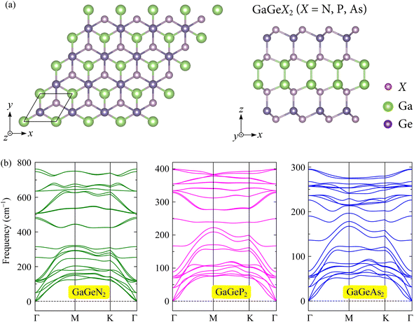 | ||
| Fig. 1 (a) Crystal structure (top and side views) and (b) phonon dispersions of GaGeX2 (X = N/P/As) monolayers. | ||
| a | dGa–Ga | dGa–X | dX–Ge | dGe–X | h | Ecoh | EPBEg | EHSE06g | EHSE+SOCg | Φ | |
|---|---|---|---|---|---|---|---|---|---|---|---|
| GaGeN2 | 3.12 | 2.46 | 1.98 | 1.88 | 1.89 | 9.02 | 7.69 | 1.75 | 2.90 | 2.89 | 6.31 |
| GaGeP2 | 3.75 | 2.47 | 2.35 | 2.33 | 2.39 | 10.96 | 5.72 | 1.08 | 1.75 | 1.70 | 5.31 |
| GaGeAs2 | 3.92 | 2.47 | 2.45 | 2.44 | 2.52 | 11.40 | 5.24 | 0.47 | 1.15 | 1.04 | 4.79 |
We then calculate the cohesive energy (Ecoh) which represents the bonding strength of atoms within the solid by using the following formula:
 | (1) |
The calculated Ecoh values are presented Table 1. The positive and high Ecoh values of the GaGeX2 monolayers suggest the high energetic stability of these systems. Among them, the GaGeN2 monolayer shows the highest cohesive energy of 7.69 eV per atom, while the GaGeP2 and GaGeAs2 have lower Ecoh of 5.72 and 5.24 eV per atom, respectively. The high Ecoh of GaGeN2 is due to its short bond lengths, leading to stronger chemical bonds of atoms in the GaGeN2 structure.
Moreover, we conduct the phonon dispersions to check the dynamic stability of the GaGeX2 systems. The phonon dispersion results of the monolayers are presented in Fig. 1(b). All three structures have twenty-four phonon branches in the phonon spectra because of the presence of eight atoms in their unit cells. It can be seen that the highest frequency of the phonon dispersions is gradually decreased as the X atom transfers from N to P/As, leading to the compression of the frequency range in the phonon bands. Besides, the intersection of acoustic and optical vibrational modes in the low-frequency ranges causes optical-acoustic scattering with low thermal conductivity. In general, the phonon dispersions of the GaGeX2 monolayers exhibit positive frequencies without the existence of imaginary frequencies over the BZ. This indicates that the GaGeX2 structures are dynamically stable.
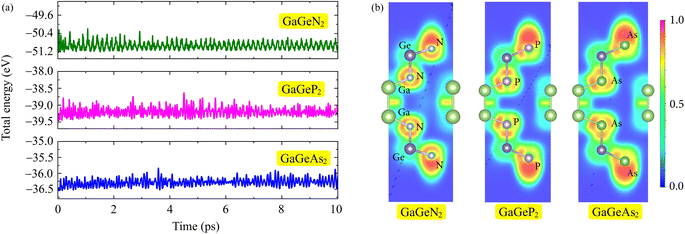
Additionally, we perform the AIMD simulations to examine the thermal stability of the GaGeX2 monolayers by heating the structures to 300 K in the duration of 10 ps. The total energy fluctuations during the simulations are depicted in Fig. 2(a). We can observe only small energies change throughout the heating, suggesting that the GaGeX2 structures are thermodynamically stable at room temperature. The electron localization functions (ELF) are also analyzed for the chemical bonding behaviours of the GaGeX2 monolayers. As presented in Fig. 2(b), the red regions for the high probability of electron localization are observed around N, P, and As atoms. Meanwhile, the electron localization is quite low around the Ga and Ge atoms, implying the charges might transfer from Ga and Ge to X atoms.
3.2 Raman active modes and vibrational properties
In this section, we examine the Raman spectra and vibrational properties of the GaGeX2 monolayers. Raman spectroscopy is considered a reliable technique for analyzing physical characteristics such as chemical composition, structural phase, and electronic structure of the materials. For Raman measurement by experiments, a light beam is focused onto the sample, and then we collect the scattered photons to evaluate the shift of light intensity dispersion for Raman responses. Similar to Raman theory, from the interaction of incident photons with molecules in the material, we can obtain Raman scattering. The energy difference of the incident and scattered photons which correlated to the vibrational mode energies can give information about the Raman shift in the Raman spectrum. In this study, we use the finite displacement approach to calculate the Raman activity tensors of phonon modes at Γ-point in the BZ. As mentioned, the GaGeX2 monolayers have the symmetry of D3h point group. The optical modes in the phonon spectra at Γ-point are either doubly degenerate or non-degenerate. The corresponding irreducible representation of the optical modes can be written as with
with  are non-degenerate out-of-plane vibrations and E′/E′′ relate to doubly degenerate in-plane vibrations. Among these vibration modes,
  E′, and E′′ are Raman active modes.
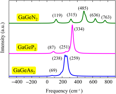
Fig. 3 illustrates the calculated Raman spectra of the GaGeX2 monolayers. We can observe that the Raman spectrum of the GaGeN2 shows five high-intensity peaks at 119, 315, 485, 636, and 763 cm−1, in which the peaks at 315, 485, and 763 cm−1 are the  phonon mode. Meanwhile, the main peaks in the Raman spectra of the GaGeP2 GaGeAs2 monolayers are located at 334 cm−1 and 238 cm−1, respectively. We can observe the change of the highest intensity peak to the lower frequency when the X element transfers from N to P/As. This correlates to the increase of the atomic mass of X in the GaGeX2 structures.
3.3 Mechanical properties and piezoelectricity
The mechanical and piezoelectric characteristics of the GaGeX2 structures are also analyzed by calculating the mechanical tensors and piezoelectric coefficients. Four different elastic constants require to find are C11, C12, C22, and C66. We have C11 = C22 due to the hexagonal structures of the GaGeX2. Thus, three elastic constants of C11, C12, and C66 are calculated by adding a strain ranging from −1.5 to 1.5% along two in-plane directions and polynomial fitting the energy changing with the applied strain.34 The attained elastic constants are presented in Table 2. The C11, C12, and C66 values vary from 161.89, 42.96, and 59.46 N m−1 for GaGeAs2 to 390.78, 118.05, and 136.36 N m−1 for GaGeN2, respectively. It can be seen that these positive elastic constants of the three monolayers satisfy the condition of C11 − C12 > 0 according to the criterion of Born–Huang for mechanical stability.35,36 This demonstrates the mechanically stable GaGeX2 structures for experimental fabrication.| C11 (N m−1) | C12 (N m−1) | C66 (N m−1) | Y2D (N m−1) | ν | e11 (10−10 C m−1) | e31 (10−10 C m−1) | d11 (pm V−1) | d31 (pm V−1) | |
|---|---|---|---|---|---|---|---|---|---|
| GaGeN2 | 390.78 | 118.05 | 136.36 | 355.11 | 0.30 | −2.37 | 0.00 | −0.87 | 0.00 |
| GaGeP2 | 197.35 | 49.78 | 73.78 | 184.79 | 0.25 | −1.60 | 0.00 | −1.09 | 0.00 |
| GaGeAs2 | 161.89 | 42.96 | 59.46 | 150.49 | 0.27 | −1.46 | 0.00 | −1.23 | 0.00 |
Next, from the obtained elastic constants, we calculate the elastic modulus for the compressive and tensile stiffness of the materials, Young's modulus (Y2D), by using the following formula:
 | (2) |
As listed in Table 2, the attained Y2D values of the GaGeX2 structures vary from 150.49 to 184.79 and 355.11 N m−1 for the GaGeAs2, GaGeP2 and GaGeN2, respectively. The decrease of Y2D when X changes from N to P and As is associated with the increase of bond lengths. Since the bond lengths of GaGeN2 are shorter than that of the GaGeP2 and GaGeAs2 monolayers, the GaGeN2 exhibits higher Y2D value. Thus the GaGeN2 is quite stiff, while the GaGeP2 and GaGeAs2 are more flexible and mechanically stable. The Y2D values of the GaGeP2 and GaGeAs2 monolayers are comparable with the reported values of SMoSiP2 (Y2D = 163.48 N m−1),37 MoSi2P4 (Y2D = 204.80 N m−1),38 and WSiP3H (Y2D = 152.47 N m−1).39
In addition, we measure the deformation of materials by calculating the Poisson's ratio ν2D of the GaGeX2 structures. The ν2D is expressed as:
 | (3) |
The obtained ν2D values are shown in Table 2. The GaGeX2 monolayers show isotropic Poisson's ratios of 0.30 for GaGeN2, 0.25 for GaGeP2, and 0.27 for GaGeAs2. These values are lower than the Poisson's ratios of ZrSiGeN4 (ν2D = 0.34)40 and Ga2STe2 (ν2D = 0.36) monolayers.16
For piezoelectric applications, we also investigate the piezoelectric effects of the GaGeX2 monolayers. When we apply a mechanical stress to a piezoelectric material, it will cause a deformation of crystal structure and generate electricity due to the imbalanced electric charge distribution. To have this interesting property, the piezoelectric material must have a noncentrosymmetric lattice structure for the electric dipole generation. The 2D Janus monolayers with anisotropic structures are expected to exhibit not only in-plane piezoelectricity but also extra out-of-plane piezoelectricity. In this work, we use the DFT calculation method reported by Duerloo and co-workers to study the piezoelectric effects of the GaGeX2.34 By analyzing the polarization changes from the applied mechanical strains, we can estimate the piezoelectric coefficients (eijk and dijk) as follows:
 | (4) |
 | (5) |
According to the calculated e11 and e31 values, the d11 and d31 are attained by using following formulas:41
 | (6) |
 | (7) |
Table 2 summarizes the resulting piezoelectric coefficient values. As depicted in Fig. 1(a), the GaGeX2 monolayers have the D3h symmetry, then they exhibit only the in-plane piezoelectric effect. Therefore, the e31 and d31 values for the out-of-plane coefficients are zero. To determine the piezoelectric coefficient, we calculate the dependence of polarization change on the small uniaxial strains.34,42 The obtained values are linearly fitted. The relaxed-ion piezoelectric coefficient determined by the slope of the line43 and the positive or negative value depends on the increasing or decreasing trend of polarization change with uniaxial strain.34,42 The obtained in-plane piezoelectric coefficients e11 and d11 for the GaGeN2, GaGeP2, and GaGeAs2 are −2.37 × 10⁻¹⁰ C m−1 and −0.87 pm V−1, −1.60 × 10⁻¹⁰ C m−1 and −1.09 pm V−1, −1.46 × 10⁻¹⁰ C m−1 and −1.23 pm V−1, respectively. Notably, when the X element changes from N to P and As, the absolute values of d11 increase. The high absolute d11 value of the GaGeAs2 monolayer are comparable with other Janus materials of WSiN3H (d11 = 0.99 pm V−1),39 MoSi2N4 (d11 = 1.144 pm V−1), and WSiGeN4 (d11 = 1.050 pm V−1),44 making this material suitable for piezoelectric applications.
3.4 Electronic properties
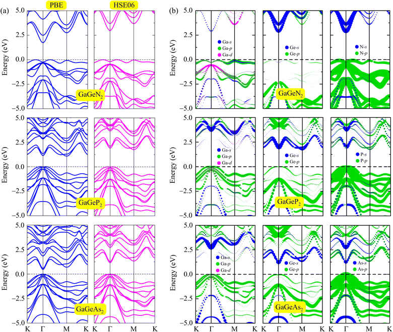
In the following, we examine the electronic properties of the GaGeX2 monolayers by calculating their band structures. As depicted in Fig. 4(a), the electronic structures calculated at the PBE level exhibit semiconductor characteristics for all three GaGeX2 systems. The obtained bandgap values (Eg) are listed in Table 1. The GaGeN2 has the highest Eg of 1.75 eV, while the Eg of GaGeP2 and GaGeAs2 are 1.08 and 0.47 eV, respectively. The GaGeN2 and GaGeP2 are found as indirect semiconductors, while the GaGeAs2 is a direct semiconductor with both conduction and valence band edges located at Γ-point in the BZ. Besides, due to the underestimated bandgap problem, the HSE06 approach is also used for estimating more accurate bandgap values. The electronic bands from the HSE06 method of the GaGeX2 monolayers show similar structures with the electronic bands from the PBE method. However, the calculated bandgap values at the HSE06 level are higher with 2.90 eV for GaGeN2, 1.75 eV for GaGeP2 and 1.15 eV for GaGeAs2 monolayer. The bandgap values of the GaGeP2 and GaGeAs2 are optimal for absorption in the visible spectrum, suggesting the potential application of these monolayers in photovoltaic devices. Additionally, we calculate the bandgap energy with the presence of spin–orbit coupling (SOC), since this SOC interaction has significant influences on the electronic band structure of the materials. The HSE06+SOC band structures and corresponding partial density of states (PDOS) of GaGeX2 monolayers are depicted in Fig. 5. It is found that the influence of SOC on the electronic bands of GaGeX2 monolayers is quite weak. When SOC is taken into account, the spin degeneracy is eliminated, however, as depicted in Fig. 5, the spin-splitting energy is insignificant. At the HSE06+SOC band gaps of GaGeN2, GaGeP2, and GaGeAs2 are found to be 2.89, 1.70, and 1.04 eV, respectively, as presented in Table 1. Thus, the bandgap of the studied materials is only reduced very slightly when SOC is included.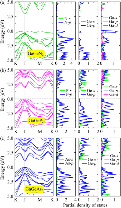 | ||
| Fig. 5 Calculated HSE06 + SOC band structures and corresponding partial density of states of GaGeN2 (a), GaGeP2 (b), and GaGeAs2 (c) monolayers. | ||
The weighted band structures of the GaGeX2 systems are also performed to elucidate the contribution of elements to the formation of electronic bands. As shown in Fig. 4(b), the GaGeP2 and GaGeAs2 monolayers have quite similar weighted band structures. In general, the p orbitals of Ga, Ge, and X atoms have strong contributions to the valence band. Especially, the valence band maximum (VBM) near the Fermi level is mainly contributed by the X-p orbitals. The Ga-s, Ge-s, and X-s orbitals also give small contributions to the valence band at low-energy regions. Meanwhile, these s orbitals of Ga, Ge, and X atoms significantly contribute to the formation of conduction band minimum (CBM). The Ge-p and X-p orbitals have weaker contributions to the conduction band of the GaGeP2 and GaGeAs2 monolayers at high energy regions. The contribution of Ga-d orbitals to both the formation of valence and conduction bands is quite small compared with other orbitals.
Next, we determine another important characteristic of the electrons, the work function Φ, which can evaluate the potential for electrons to leave the surface of materials. Based on the calculation of electrostatic potentials, Φ is estimated from the vacuum level (Evac) and Fermi level (EF) by following equation:
| Φ = Evac − EF. | (8) |
Fig. 6 illustrates the planar electrostatic potentials of the GaGeX2 monolayers. It can be observed the decrease of work function when the X atom transfers from N to P/As. The GaGeN2 has a higher work function than that of the GaGeP2 and GaGeAs2 structures. This indicates that the electrons can escape from the surface of GaGeP2 and GaGeAs2 more easily than the GaGeN2 surface. The obtained work function values vary from 4.79 eV for GaGeAs2 to 6.31 eV for GaGeN2 as summarized in Table 1.
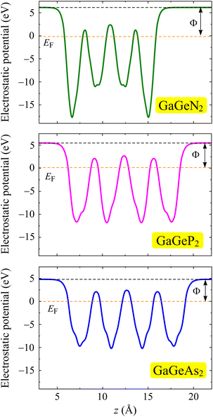 | ||
| Fig. 6 Electrostatic potential of GaGeX2 monolayers with the dipole correction. The dashed orange lines indicate the Fermi level. | ||
3.5 Transport properties
To evaluate the applicability for electronic applications of the materials, we examine the transport properties of the GaGeX2 monolayers. An important factor directly related to the charge transport is the carrier mobilities μ2D, which can be determined by using the DP approximation as the following:32,45
 | (9) |
 refer to the carrier effective mass and average effective mass, respectively. Ed relates to the DP constant and C2D is the elastic modulus.
Thus to estimate the carrier mobilities μ2D, we have to find the carrier effective mass m*, the elastic modulus C2D, and the DP constant Ed. Among these parameters, the C2D can be expressed as:
 | (10) |
 | (11) |
The uniaxial strain (εunix/y) is added along the x and y axes, with a range of −1 to 1%, for the calculations. The values of C2D and Ed can be achieved by fitting the dependence of applied strain with energy and band edges.44,45 Fig. 7 depicts the changing energy and positions of band edges of the GaGeX2 monolayers. We can observe that the C2D of all three structures is directional isotropic. The calculated C2D values are almost the same between the two different x and y directions as listed in Table 3. Besides, the band edge positions of the GaGeN2, GaGeP2, and GaGeAs2 monolayers along the two in-plane directions are almost the same. The GaGeX2 monolayers show anisotropic DP constants along the transport directions with the Ed values ranging from −15.59 to −4.77 eV. Some other Janus materials are also found to have the anisotropic DP constant such as Ga2Te3,46 STiSiAs2,47 and Ga2SX2.16 This anisotropic Ed can lead to the anisotropy of carrier mobility of the GaGeX2 monolayers.
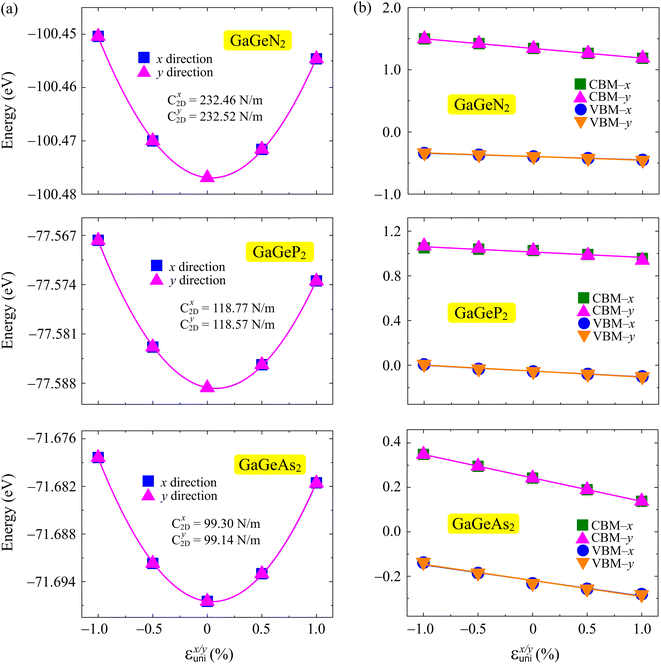 | ||
| Fig. 7 The total energy (a) and band edges (b) dependence on applied strains in the x/y directions of GaGeX2 systems. The fitted curves are indicated by the solid lines. | ||
| C2Dx | C2Dy | Edx | Edy | μx | μy | ||||
|---|---|---|---|---|---|---|---|---|---|
| Electron | GaGeN2 | 0.21 | 0.23 | 232.46 | 232.52 | −15.59 | −15.59 | 447.33 | 415.23 |
| GaGeP2 | 0.41 | 0.30 | 118.77 | 118.57 | −4.77 | −6.39 | 776.95 | 578.63 | |
| GaGeAs2 | 0.09 | 0.11 | 99.30 | 99.14 | −10.55 | −10.54 | 2270.17 | 1788.59 | |
| Hole | GaGeN2 | 4.70 | 1.73 | 232.46 | 232.52 | −5.51 | −5.85 | 12.19 | 29.41 |
| GaGeP2 | 7.74 | 1.38 | 118.77 | 118.57 | −5.23 | −5.40 | 3.65 | 19.24 | |
| GaGeAs2 | 0.77 | 0.68 | 99.30 | 99.14 | −7.10 | −7.27 | 75.06 | 80.38 |
The carrier effective mass m*, which has a significant impact on the mobility of carriers, can be derived as follows:
 | (12) |
 in the x direction of 7.74m0. In general, the effective masses of holes for the three monolayers are higher than the effective masses of electrons. This is in good agreement with the flatter band diagram around the valence band edge compared with the conduction band edge as presented in Fig. 4(a). The high hole effective masses may lead to low hole mobilities due to their slow response to the external electric field.
According to the obtained parameters of Ed, C2D, and m*, we can find the values of carrier mobilities μ2D by using eqn (9). The calculated carrier mobilities of all three monolayers are listed in Table 3. The μ2D values of the GaGeX2 are anisotropic in the two in-plane directions for both electrons and holes. As expected from the effective mass results, the electron mobilities of all three GaGeX2 monolayers are higher than the hole mobilities. In particular, the GaGeN2 and GaGeP2 structures have quite low hole mobilities of 3.65 to 29.41 cm2 V−1 s−1 for both the two in-plane directions, while the GaGeAs2 monolayer exhibits the highest electron mobilities of 2270.17 and 1788.59 cm2 V−1 s−1 for the x and y directions, respectively. The GaGeN2 and GaGeP2 show lower electron mobilities of 447.33 and 776.95 cm2 V−1 s−1 in the x direction, respectively. The obtained electron mobility of the GaGeAs2 monolayer is higher than that of the other reported Janus materials of Ga2SSe2,16 In2SeO,17 MoSiAs3H,19 and WSiAs3H.39 The anisotropic and high electron mobility of the GaGeAs2 monolayer shows potential applications of this material in the electronic fields.
4 Conclusion
In summary, we have conducted first-principles calculations to examine the crystal structures and physical characteristics of the GaGeX2 monolayers. Our analyses of the cohesive energy, phonon dispersion spectra, and AIMD simulations demonstrate that the three proposed structures have good energetic, dynamic, and thermodynamic stabilities. The Raman spectra are performed for the Raman activities and vibrational properties of the GaGeX2 systems. From the calculated piezoelectric coefficients, the GaGeX2 are found as piezoelectric materials with the high d11 of −1.23 pm V−1 for the GaGeAs2 monolayer. Our PBE and HSE06 investigations reveal that the GaGeX2 are semiconductors with moderate bandgap energies. At the HSE06 level, the GaGeP2 and GaGeAs2 structures exhibit optimal bandgaps for photovoltaic applications of 1.75 and 1.15 eV, respectively. Moreover, all three investigated GaGeX2 systems have anisotropic carrier mobility in the two in-plane directions for both electrons and holes. Among them, the GaGeAs2 monolayer shows the highest electron mobilities of 2270.17 and 1788.59 cm2 V−1 s−1 for the x and y directions, respectively. With high electron mobility, large piezoelectric coefficient, and optimal bandgap energy, the GaGeAs2 material holds potential applicability for applications in multifunctional devices.Data availability
All data that support the findings of this study are included within the article.Conflicts of interest
There are no conflicts of interest to declare.References
- H. Zhao, Y. Gu, N. Lu, Y. Liu, Y. Ding, B. Ye, X. Huo, B. Bian, C. Wei, X. Zhang and G. Yang, Chem. Phys., 2022, 553, 111384 CrossRef CAS.
- V. D. Dat and T. V. Vu, New J. Chem., 2022, 46, 1557–1568 RSC.
- M. Dragoman, A. Dinescu and D. Dragoman, Phys. Status Solidi A, 2019, 216, 1800724 CrossRef.
- Z. Liu, H. Wang, J. Sun, R. Sun, Z. F. Wang and J. Yang, Nanoscale, 2018, 10, 16169–16177 RSC.
- F. R. Fan, R. Wang, H. Zhang and W. Wu, Chem. Soc. Rev., 2021, 50, 10983–11031 RSC.
- Y. Zhu, L. Peng, Z. Fang, C. Yan, X. Zhang and G. Yu, Adv. Mater., 2018, 30, 1706347 CrossRef PubMed.
- T. Tan, X. Jiang, C. Wang, B. Yao and H. Zhang, Adv. Sci., 2020, 7, 2000058 CrossRef CAS PubMed.
- H. Zhu, Y. Wang, J. Xiao, M. Liu, S. Xiong, Z. J. Wong, Z. Ye, Y. Ye, X. Yin and X. Zhang, Nat. Nanotechnol., 2014, 10, 151–155 CrossRef PubMed.
- C. Zhang, Y. Nie, S. Sanvito and A. Du, Nano Lett., 2019, 19, 1366–1370 CrossRef CAS PubMed.
- M. Tahir, N. Fatima, U. Fatima and M. Sagir, Inorg. Chem. Commun., 2021, 124, 108242 CrossRef CAS.
- X. Liu, S. Zhang, S. Guo, B. Cai, S. A. Yang, F. Shan, M. Pumera and H. Zeng, Chem. Soc. Rev., 2020, 49, 263–285 RSC.
- N. K. Chaudhari, H. Jin, B. Kim, D. San Baek, S. H. Joo and K. Lee, J. Mater. Chem. A, 2017, 5, 24564–24579 RSC.
- C.-H. Lai, M.-Y. Lu and L.-J. Chen, J. Mater. Chem., 2012, 22, 19–30 RSC.
- T. Kajana, A. Pirashanthan, D. Velauthapillai, A. Yuvapragasam, S. Yohi, P. Ravirajan and M. Senthilnanthanan, RSC Adv., 2022, 12, 18041–18062 RSC.
- M. Bikerouin, O. Chdil and M. Balli, Nanoscale, 2023, 15, 7126–7138 RSC.
- N. N. Hieu, H. V. Phuc, A. I. Kartamyshev and T. V. Vu, Phys. Rev. B, 2022, 105, 075402 CrossRef CAS.
- T. V. Vu, C. V. Nguyen, H. V. Phuc, A. A. Lavrentyev, O. Y. Khyzhun, N. V. Hieu, M. M. Obeid, D. P. Rai, H. D. Tong and N. N. Hieu, Phys. Rev. B, 2021, 103, 085422 CrossRef CAS.
- I. Bouziani, M. Kibbou, Z. Haman, N. Khossossi, I. Essaoudi, A. Ainane and R. Ahuja, Phys. E, 2021, 134, 114900 Search PubMed.
- X. Cai, G. Chen, R. Li, W. Yu, X. Yang and Y. Jia, Phys. Chem. Chem. Phys., 2023, 25, 29594–29602 RSC.
- J. Wang, H. Guo, J. Xue, D. Chen, G. Yang, B. Liu, H. Lu, R. Zhang and Y. Zheng, Sol. RRL, 2019, 3, 1900321 Search PubMed.
- L. Dong, J. Lou and V. B. Shenoy, ACS Nano, 2017, 11, 8242–8248 CrossRef CAS PubMed.
- Y. Cui, L. Peng, L. Sun, M. Li, X. Zhang and Y. Huang, J. Phys.: Condens.Matter, 2019, 32, 08LT01 CrossRef PubMed.
- G. Kresse and J. Furthmüller, Phys. Rev. B: Condens. Matter Mater. Phys., 1996, 54, 11169–11186 CrossRef CAS PubMed.
- G. Kresse and J. Furthmüller, Comput. Mater. Sci., 1996, 6, 15–50 CrossRef CAS.
- P. E. Blöchl, Phys. Rev. B: Condens. Matter Mater. Phys., 1994, 50, 17953 CrossRef PubMed.
- G. Kresse and D. Joubert, Phys. Rev. B: Condens. Matter Mater. Phys., 1999, 59, 1758–1775 CrossRef CAS.
- J. P. Perdew, K. Burke and M. Ernzerhof, Phys. Rev. Lett., 1996, 77, 3865 CrossRef CAS PubMed.
- A. Togo, L. Chaput and I. Tanaka, Phys. Rev. B: Condens. Matter Mater. Phys., 2015, 91, 094306 CrossRef.
- J. Heyd, G. E. Scuseria and M. Ernzerhof, J. Chem. Phys., 2003, 118, 8207 CrossRef CAS.
- S. Grimme, J. Antony, S. Ehrlich and H. Krieg, J. Chem. Phys., 2010, 132, 154104 CrossRef PubMed.
- M. Yagmurcukardes, F. M. Peeters and H. Sahin, Phys. Rev. B, 2018, 98, 085431 CrossRef CAS.
- J. Bardeen and W. Shockley, Phys. Rev., 1950, 80, 72 CrossRef CAS.
- T. V. Vu, V. T. T. Vi, N. T. Hiep, K. V. Hoang, A. I. Kartamyshev, H. V. Phuc and N. N. Hieu, RSC Adv., 2024, 14, 21982–21990 RSC.
- K.-A. N. Duerloo, M. T. Ong and E. J. Reed, J. Phys. Chem. Lett., 2012, 3, 2871–2876 CrossRef CAS.
- R. C. Andrew, R. E. Mapasha, A. M. Ukpong and N. Chetty, Phys. Rev. B: Condens. Matter Mater. Phys., 2012, 85, 125428 CrossRef.
- N. T. Hung, A. R. T. Nugraha and R. Saito, J. Phys. D: Appl. Phys., 2018, 51, 075306 CrossRef.
- N. T. Hiep, C. Q. Nguyen, N. A. Poklonski, C. A. Duque, H. V. Phuc, D. V. Lu and N. N. Hieu, J. Phys. D: Appl. Phys., 2023, 56, 385306 CrossRef CAS.
- Y. Liu, C. Shao, W. Yu, Q. Gui, J. Robertson and Y. Guo, Appl. Phys. Lett., 2022, 121, 244105 CrossRef CAS.
- T. V. Vu, B. D. Hoi, A. I. Kartamyshev and N. N. Hieu, J. Appl. Phys., 2024, 135, 074301 CrossRef CAS.
- V. T. T. Vi, T. P. T. Linh, C. Q. Nguyen and N. N. Hieu, Adv. Theory Simul., 2022, 5, 2200499 CrossRef CAS.
- Y. Guo, S. Zhou, Y. Bai and J. Zhao, Appl. Phys. Lett., 2017, 110, 163102 CrossRef.
- M. T. Ong and E. J. Reed, ACS Nano, 2012, 6, 1387–1394 CrossRef CAS PubMed.
- H.-N. Zhang, Y. Wu, C. Yang, L.-H. Zhu and X.-C. Wang, Phys. Rev. B, 2021, 104, 235437 CrossRef CAS.
- S.-D. Guo, W.-Q. Mu, Y.-T. Zhu, R.-Y. Han and W.-C. Ren, J. Mater. Chem. C, 2021, 9, 2464–2473 RSC.
- W. Wan, S. Zhao, Y. Ge and Y. Liu, J. Phys.: Condens.Matter, 2019, 31, 435501 CrossRef CAS PubMed.
- C.-F. Fu, J. Sun, Q. Luo, X. Li, W. Hu and J. Yang, Nano Lett., 2018, 18, 6312–6317 CrossRef CAS PubMed.
- Z. Gao, X. He, W. Li, Y. He and K. Xiong, Dalton Trans., 2023, 52, 8322–8331 RSC.
| This journal is © The Royal Society of Chemistry 2024 |

