 Open Access Article
Rapid activation of a solution-processed aluminum oxide gate dielectric through intense pulsed light irradiation
Yeon-Wha Oh ab,
Hoon Kimc,
Lee-Mi Doc,
Kyu-Ha Baekc,
Il-Suk Kanga,
Ga-Won Lee*b and
Chan-mo Kang
 *c
*c
aDivision of Nano Convergence Technology Development, Nantional NanoFAB Center, Daejeon, 34141, South Korea
bDept. of Electronics Engineering, Chungnam National University, Daejeon, 34134, South Korea. E-mail: gawon@cnu.ac.kr
cElectronics and Telecommunications Research Institute, 218 Gajeong-ro, Yuseong-gu, Daejeon, 34129, South Korea. E-mail: nkcm@etri.re.kr; Fax: +82-42-860-5202; Tel: +82-42-860-5229
First published on 22nd November 2024
Abstract
In this study, we report rapid activation of a solution-processed aluminum oxide gate dielectric film to reduce its processing time under ambient atmosphere. Aluminum precursor films were exposed to a high energy light-pulse and completely converted into dielectric films within 30 seconds (450 pulses). The aluminum oxide gate dielectric film irradiated using intense pulsed light with 450 pulses exhibits a smooth surface and a leakage current density of less than 10−8 A cm−2 at 2 MV cm−1. Moreover, dielectric constants of the aluminum oxide layer were calculated to be approximately 7. Finally, we fabricated a solution-processed indium gallium zinc oxide thin-film transistor with AlOx using intense pulsed light irradiation, exhibiting a field-effect mobility of 2.99 cm2 V−1 s−1, threshold voltage of 0.73 V, subthreshold swing of 180 mV per decade and Ion/Ioff ratio of 3.9 × 10⁶.
Introduction
Metal oxide thin-film transistors (TFTs) represent a new era of display applications because of their high transparency, large-area uniformity, and high mobility.1–3 In particular, metal oxide materials can be applied in TFTs as semiconductors, transparent electrodes, and insulators.4–9 Among these, insulators play an important role in TFTs because they determine the breakdown voltage, leakage current, and charge accumulation at the dielectric/semiconductor interface.10 Silicon dioxide (SiO2) has mainly been adopted as a gate insulator in oxide TFTs, but various high dielectric constant (high-κ) materials such as yttrium trioxide, zirconium oxide (ZrO2), hafnium dioxide, and aluminum oxide (AlOx) have recently been researched to reduce leakage currents and achieve high capacitance.11–17High-κ gate dielectric films must have smooth surfaces and dense structures to achieve low leakage current, stable operation, and high breakdown voltage. Among these, aluminum oxide is the most attractive material because of its low interface trap density with oxide semiconductors, high breakdown field, and smooth surface. Generally, AlOx is deposited using vacuum-based processes such as atomic layer deposition, chemical vapor deposition, and sputtering; however, these methods have been limited by the lack of low-cost devices. A simple solution process, which converts a metal precursor film into a metal oxide one via annealing, can be a cost-effective alternative because it can easily form AlOx at an affordable cost.18,19 To realize high-performance solution-processed oxide gate dielectrics, several annealing processes have been proposed such as thermal,20,21 deep ultra-violet (DUV),22,23 and microwave-assisted annealing,24 which effectively remove metal ligands and other chemical impurities during metal-oxide framework formation. However, these methods require more than an hour, which is an obstacle to mass production. Therefore, the development of a novel rapid annealing method for metal oxide insulators is indispensable.
The intense pulsed light (IPL) process uses a xenon flash lamp to deliver high energy pulsed light, so that thin films can be rapidly sintered from a precursor film to a metal oxide film. IPL annealing has been applied for metal oxide semiconductor annealing,25,26 metal ink sintering,27,28 nanoparticle sintering,29 and sterilization.30 However, most studies that apply IPL methods for the formation of metal oxide films have concentrated on semiconductor or electrode variants, with insufficient research on metal oxide gate dielectrics. Recently, several studies have explored the IPL processing method for gate insulators, including notable research studies by Yarali et al.31 and Carlos et al.32 Yarali et al. reported solution-processed Al2O3/ZrO2 bilayer dielectric films sintered using IPL, but the dielectric films exhibited low breakdown voltage and high leakage current and are therefore unsuitable for use as a gate insulator. Carlos et al. reported the ultrafast combustion synthesis of solution-based AlOx films using excimer laser annealing. The AlOx film showed suitable breakdown voltage and leakage current with a short processing time. However, this method has the drawback of low large-area uniformity and productivity due to the small laser spot size. Herein, we fabricated a solution-processed AlOx film by employing IPL annealing. We investigated the effects of IPL on the solution-processed AlOx film by increasing the number of IPL pulses (PIPL) and analyzed its physical, chemical, and electrical characteristics as a function of PIPL. We demonstrated a rapid manufacturing method using IPL within 30 seconds, which resulted in a dense AlOx thin film with good electrical characteristics such as high breakdown voltage and low leakage current. Finally, we confirmed that the AlOx film was suitable to be used as a gate insulator by fabricating indium-gallium-zinc oxide (IGZO) TFTs through the IPL process.
Experimental
Precursor solution synthesis
A 0.6 M aluminum oxide gate dielectric precursor solution was prepared by dissolving aluminum nitrate nonahydrate (AlN3O9·9H2O, Sigma-Aldrich) in 2-methoxyethanol. The aluminum oxide solution was stirred vigorously at 75 °C for 6 hours under ambient conditions. An IGZO precursor solution was prepared by dissolving indium nitrate nonahydrate (InN6O9·9H2O, Alfa-Aesar), gallium nitrate hydrate (GaN3O9·xH2O, Sigma-Aldrich), and zinc nitrate hexahydrate (ZnN2O6·6H2O, Sigma-Aldrich) in 2-methoxyethanol at concentrations of 0.1 M in a molar ratio of 7![[thin space (1/6-em)]](https://www.rsc.org/images/entities/char_2009.gif) :
:![[thin space (1/6-em)]](https://www.rsc.org/images/entities/char_2009.gif) 1.5
1.5![[thin space (1/6-em)]](https://www.rsc.org/images/entities/char_2009.gif) :
:![[thin space (1/6-em)]](https://www.rsc.org/images/entities/char_2009.gif) 1.5. The IGZO solution was stirred at 1500 rpm for 6 hours at room temperature. All the precursor solutions were kept under ambient conditions for a day before use.
1.5. The IGZO solution was stirred at 1500 rpm for 6 hours at room temperature. All the precursor solutions were kept under ambient conditions for a day before use.
Thin film fabrication and characterization
Both metal oxide thin films were fabricated on 2 × 2 cm2 heavily p-doped silicon wafers, which were ultrasonically cleaned in acetone, isopropyl alcohol, and deionized water. To remove the remaining water, the substrates were annealed at 120 °C on a hotplate for 10 min. Next, the substrates were treated with ultraviolet ozone (UVO) for 10 min. The aluminum oxide solution was filtered through a 0.2 μm syringe filter (HP020, Advantec) and then spun on the UVO-treated substrates at 3000 rpm for 60 s. Before IPL irradiation, aluminum oxide precursor thin films were annealed at 100 °C for 10 min under ambient atmosphere to remove the solvents. Thereafter, the AlOx thin films were irradiated with IPL for 0–450 pulses in the air using xenon flash lamp equipment manufactured by PRO WIN Co., Ltd. The xenon lamp emitted a broad spectrum of light ranging from ultraviolet to infrared region similar to sunlight, covering wavelengths from 200 nm to 2000 nm. The distance between the lamp and the sample was set to 0.5 cm during the IPL process. The frequency and energy of the pulsed light were 15 Hz and 207 J per pulse, respectively. The pulse duration and period were 0.5 ms and 66.7 ms, respectively. The thicknesses of the sol–gel-derived AlOx films with PIPL were measured using field emission–scanning electron spectroscopy (FESEM, HITACHI SU8230). The average thickness and standard deviation of the AlOx films were calculated based on three measurement points. The morphologies of the films were characterized through atomic force microscopy (AFM, HORIBA INNOVA-LABRAM HR800) in the tapping mode. X-ray photoelectron spectroscopy (XPS, Thermo VG Scientific Sigma Probe) was employed to obtain the metal–oxygen binding state of the AlOx dielectric films.Device fabrication and characterization
To measure insulator properties, an Al electrode (60 nm) was deposited on AlOx/p+-Si substrates via thermal evaporation. The area of the Al electrode was 500 μm × 500 μm. The capacitance of the dielectric films was measured with a precision LCR meter (HP4284A). The leakage current of the dielectrics and electrical properties of metal–insulator–metal (MIM) devices were measured with a precision semiconductor analyzer (Keithley 4200) in the dark at room temperature. To fabricate IGZO TFTs on AlOx dielectrics, the 0.1 M IGZO precursor solution was spin-coated on AlOx at 3000 rpm for 60 s and irradiated with PIPL = 150 × 3. The Al source and drain electrodes were evaporated on the IGZO channel layer. Here, the channel width-to-channel length ratio (W/L) was 7.5 (channel length = 200 μm). The electrical properties of the TFT devices were measured with a semiconductor parameter analyzer (Keithley 4200) in a dark box. Saturation mobility (μsat) was calculated using the following equation.
 | (1) |
Results and discussion
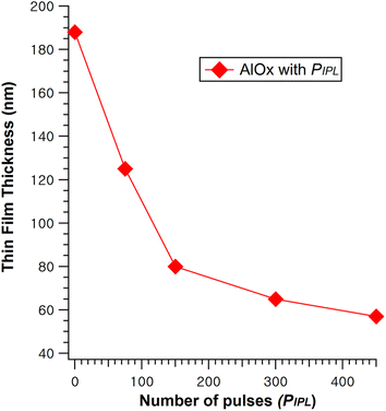
Fig. 1 shows the variation in the of the AlOx films investigated using FESEM measurements. The thicknesses of AlOx films irradiated with IPL at 0, 75, 150, 300, and 450 pulses were 188, 125, 80, 65, and 57 nm, respectively. It is clearly observed that the thickness of the film gradually decreases as the PIPL increases, which is due to the reduced residual ligand and solvent as well as the densified metal oxide framework during the IPL-driven decomposition process.33 The thickness of the controlled film with thermal annealing at 350 °C for 1 hour was 64 nm. Therefore, the AlOx dielectric film with a PIPL of more than 300 pulses, where the thickness is thinner than 64 nm, is as dense as the thermally annealed film.Generally, the surface roughness of a dielectric thin film is critical for charge accumulation at the dielectric/oxide semiconductor interface. The roughness of a dielectric film strongly affects device uniformity and stability. Surface morphologies of the IPL-irradiated AlOx films were investigated using AFM, as shown in Fig. 2. The root-mean-square roughnesses (RRMS) of the AlOx film with PIPL values of 0, 75, 150, 300, 450 were 0.21, 0.17, 0.18, 0.11, and 0.11 nm, respectively, which is comparable to that of the thermally annealed film (0.12 nm). The RRMS of the AlOx thin films tend to decrease as the PIPL increases from 0 to 450 pulses, and this tendency is consistent with that of the film thicknesses mentioned above. Therefore, the high energy of the light makes the exposed films denser and smoother, thus improving device uniformity and stability.
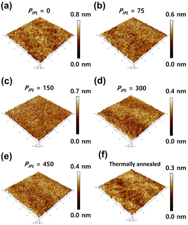 | ||
| Fig. 2 AFM images of the AlOx thin film: (a) PIPL = 0, (b) PIPL = 75, (c) PIPL = 150, (d) PIPL = 300 (e) PIPL = 450, and (f) thermally annealed. | ||
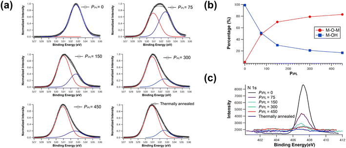
To verify the chemical composition of AlOx thin films, XPS analysis was carried out. Fig. 3 shows the XPS O 1s spectra of the AlOx films at different PIPL values, which can be deconvoluted into two peaks: (i) oxygen in metal–oxide–metal (M–O–M) bonds at 531 eV and (ii) oxygen in hydroxide-related (M–OH) bonds at 532.7 eV.10 The M–O–M and M–OH peaks of the thermally activated AlOx film are 79% and 21%, respectively. XPS O 1s peaks associated with the M–O–M lattice increase from 1% to 83% and that with the M–OH lattice decreases from 99% to 17% as the PIPL increases from 0 to 450. Before IPL annealing, the remaining metal ligand and solvent in the precursor film contain a number of M–OH bonds, resulting in high M–OH in O 1s XPS spectra. During the annealing process, the M–OH bonds in the film were converted into M–O–M bonds via decomposition and densification reactions, thus increasing the M–O–M composition ratio.34 At PIPL >300, a high composition ratio of the M–O–M bond in the AlOx films can be achieved, which is comparable to that in thermally annealed AlOx. Thus, the high concentration of M–O–M bonds indicates that the AlOx film is properly formed by IPL. Additionally, the residual quantities of nitrogen element within the dielectric layer were also scrutinized to verify metal oxide formation. The disappearance of nitrogen element within the film indicates that IPL irradiation effectively decomposes the aluminum nitrate precursor by eliminating nitrate ligands. As shown in Fig. 3c, the N 1s peak decreases as the irradiation pulse increases. Hence, the XPS data indicate that AlOx films are properly formed using IPL with a PIPL >300. Note that the frequency of IPL is 15 Hz, which means that the precursor is fully converted into AlOx within 20 s via IPL process, which is much faster than thermal annealing (more than 1 hour).
To characterize the dielectric properties of the AlOx films irradiated with IPL, a MIM device with a structure of Al/AlOx/p+-Si was employed. Fig. 4a shows the capacitance–frequency (C–F) curves of the AlOx insulators ranging from 100 Hz to 100 kHz. The capacitances for PIPL = 0 and 75 at low frequencies could not be measured, likely owing to the resistive characteristics of undecomposed films. The areal capacitance of AlOx films with a PIPL of 150, 300, and 450 was determined to be 67, 96, and 107 nF cm−2 at 100 kHz, respectively, as summarized in Table 1. The relatively low capacitance of the AlOx film with a PIPL of less than 150 can be attributed to imperfect M–O–M bonds, which result from undecomposed residuals and remaining solvent. Besides, capacitance tends to rapidly decrease as frequency increases. When the PIPL is > 300, capacitance changes in the AlOx film with respect to frequency are insignificant, caused by much lower residual impurities such as M–OH and nitrogen elements.35 The dielectric constant of a solution-processed AlOx insulator was calculated using the following formula.
 | (2) |
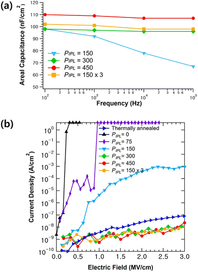 | ||
| Fig. 4 Electrical characteristics of the solution-processed AlOx thin film with varying PIPL: (a) capacitance–frequency (C–F) plot. (b) Leakage current density–electric field (J–E) plot. | ||
| Irradiation pulses (PIPL) | Thickness (nm) | Roughness (nm) | Capacitance at 100 kHz (nF cm−2) | Dielectric constant | Leakage (A cm−2) at 2 mV cm−1 |
|---|---|---|---|---|---|
| 0 | 188 ± 1.2 | 0.21 | 28 | — | — |
| 75 | 125 ± 3.7 | 0.17 | 24 | — | — |
| 150 | 80 ± 1.2 | 0.18 | 67 | — | 4.0 × 10⁻⁴ |
| 300 | 65 ± 0.9 | 0.11 | 96 | 7.1 | 4.4 × 10⁻⁹ |
| 450 | 57 ± 0.5 | 0.11 | 107 | 6.9 | 1.9 × 10⁻⁹ |
| 150 × 3 | 63 ± 0.5 | 0.12 | 98 | 7.0 | 4.3 × 10⁻⁹ |
| Thermally annealed | 64 ± 7.4 | 0.12 | 99 | 7.2 | 3.0 × 10⁻⁸ |
Fig. 4b shows the leakage current density–electric field (J–E) characteristics of AlOx films as a function of PIPL. In the case of AlOx with PIPL ≤ 150, its leakage current density was measured to be more than 10−4 A cm−2 at 2 MV cm−1, making it difficult to use as a gate insulator. It is known that the leakage current of a film should be lower than 10−6 A cm−2 to employ it as a gate insulator.36 On increasing the irradiation pulses from 150 to 450, leakage current is reduced to less than 10−8 A cm−2 at 2 MV cm−1, which is comparable to that of previously reported solution-processed gate insulators.37–39 As mentioned earlier, these excellent dielectric properties of IPL-annealed AlOx can be attributed to the formation of high-composition M–O–M bonds during high-energy pulse irradiation, which can improve the frequency dependence of capacitance.
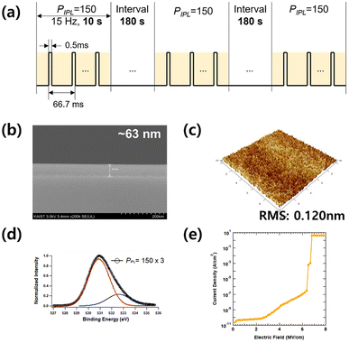
As the IPL irradiation pulse increases, dielectric properties, such as leakage current, capacitance, and roughness, of the thin film enhanced. A PIPL of 450 is an optimum condition for forming the AlOx film with low leakage current and high capacitance. However, continuous pulsed light irradiation can cause substrate overheating, which can be a problem in the case of plastic substrates because of thermal expansion mismatch and deformation. Our previous research showed that substrate temperatures after the IPL process at PIPL = 75, 150, 300, and 450 were measured to be 131.5 °C, 205.8 °C, 272.8 °C and 297.0 °C, respectively.25 Therefore, to keep substrate temperature below 200 °C while maintaining the total irradiation, a PIPL of 150 was irradiated three times with an interval of 3 min. Fig. 5a shows a schematic of the PIPL = 150 × 3. To confirm the dielectric integrity of the AlOx film with PIPL = 150 × 3, the physical, chemical and electrical properties of the film and MIM device were fully characterized. The SEM and AFM images of the dielectric film with PIPL = 150 × 3 are shown in Fig. 5a and b. The thickness of the AlOx film is approximately 60 nm, and its surface morphology exhibits a uniform surface with an RRMS value of 0.120 nm. As shown in Fig. 5c, the M–O–M and M–OH lattice peaks were determined to be 80% and 20%, respectively. From physical and chemical analysis, it is considered that the IPL irradiation of PIPL = 150 × 3 transfers enough energy to form a dense AlOx film, comparable to the thermally annealed AlOx film and PIPL = 450-irradiated one. To verify the electrical characteristics of AlOx with PIPL = 150 × 3, the breakdown field and leakage current density are presented in Fig. 5d. The electrical properties of the MIM devices exhibit low leakage current (<10−8 A cm−2 at 2 MV cm−1) and high breakdown field (>6 MV cm−1). Note that because the operating field of typical TFTs is −3 MV cm−1–+3 MV cm−1, the TFT employing the AlOx film with PIPL = 150 × 3, annealed within only 30 s under ambient conditions, could be properly operated without breakdown. Table 2 summarizes the properties of AlOx dielectric films fabricated through various photonic-assisted processing methods. Compared to films reported in previous studies, the film achieved in this study demonstrates both superior electrical properties, such as a high breakdown field (>6 MV cm−1) and low leakage current (<10−8 A cm−2 at 2 MV cm−1), as well as a short processing time (<1 min).
| References | Material | Processing method | Processing time (min) | Thickness (nm) | Roughness (nm) | Dielectric constant (k) | Breakdown field (MV cm−1) | Leakage current density at 2 MV cm−1 (A cm−2) |
|---|---|---|---|---|---|---|---|---|
| 22 | Al2O3 | DUV | 120 | 47 | 0.226 | 8 | >6 | ∼1 × 10⁻⁸ |
| 30 | ZrO2/Al2O3 | IPL | ≤1 | 30 | 0.430 | — | 1 | <1 × 10⁻⁵ at 1 MV cm−1 |
| 31 | AlOx | Excimer laser | ≤1 | 15 | 2.8 | ∼9 | 4 | ∼1 × 10⁻⁶ |
| 38 | AlOx | UV + thermal | 140 | 50 | 0.260 | 6–8 | 5.1 | ∼5 × 10⁻⁶ at 1 MV cm−1 |
| 39 | AlOx/YAlOx | DUV | 165 | 30 | — | ∼10 | — | — |
| This work | AlOx | IPL | ≤1 | 63 | 0.120 | 7 | >6 | 4.3 × 10⁻⁹ |
To evaluate the feasibility of the AlOx dielectric film with PIPL = 150 × 3, solution-processed metal oxide TFTs were fabricated using AlOx gate dielectrics and IGZO semiconducting layer irradiated with IPL on the p++ Si substrate. The transfer characteristic of the IGZO TFT with the IPL process is shown in Fig. 6a. The transfer curves of the IGZO/AlOx TFT exhibits a μsat of 2.99 cm2 V−1 s−1, Vth of 0.73 V, and Ion/Ioff ratio of 3.9 × 10⁶. Generally, hysteresis may be related to charge trapping/de-trapping behavior at the semiconductor/dielectric interface. For AlOx/IGZO TFTs, transfer curves with lower hysteresis properties are possibly due to the smooth surface roughness and high M–O–M conversion ratio. From statistical data, averaged values over 15 IGZO/AlOx devices indicate a highly uniform distribution, as shown in Fig. 6b. Note that the electrical performance with a μsat of 2.31 cm2 V−1 s−1 and low hysteresis of the IGZO/AlOx TFTs demonstrates that excellent interfacial properties and a high-quality sol–gel oxide film structure can be obtained via rapid activation with PIPL = 450 despite a short irradiation time (<30 seconds). This result attests that the rapid activation process enabled the conversion of the solution-processed oxide-based materials into highly stable and reliable gate dielectrics and semiconductors.
Conclusion
In summary, we present a novel IPL annealing method for the rapid activation of a solution-processed high-κ dielectric film. When the AlOx film was formed by irradiating IPL in the range of 0–450, the thickness of the dielectric thin film tended to decrease from 188 nm to 57 nm. Likewise, AFM analysis of AlOx with PIPL represents a flat surface roughness of ≤0.2 nm. When the aluminum precursor film was irradiated with IPL for ≥300 pulses, XPS analysis shows that the M–O–M bond ratio was 80%, and residual amounts of nitrogen element were effectively removed, indicating that the decomposition and densification reactions occurred as the IPL irradiation pulse increased. The resulting AlOx dielectric film at PIPL = 450 exhibits high electrical performance, including a large area-capacitance of 109 nF cm−2 and low leakage current density of <10−8 A cm−2 at 2 MV cm−1. In order to prevent the lamp from overheating, an AlOx thin film was formed at PIPL = 150 × 3. The optimized AlOx/IGZO TFTs with PIPL = 150 × 3 exhibit a μsat of 2.99 cm2 V−1 s−1, Vth of 0.73 V, S.S of 180 mV per decade, Ion/Ioff of 3.9 × 10⁶, and low operating voltage of 10 V. Herein, AlOx dielectric thin film with PIPL was fabricated under simple, ambient conditions and at low cost. Thus, the comprehensive investigation of their spectroscopic analysis and electrical properties demonstrates their potential as a promising high-κ dielectric for low-voltage high-performance oxide TFT devices. It is expected that the results obtained in this research can be widely used in the application of gate dielectric layers for metal oxide electronic devices.Data availability
The data supporting the findings of this study are available within the article.Conflicts of interest
There are no conflicts to declare.Acknowledgements
This work was partially supported by the Technology Innovation Program (RS-2023-00257784, RS-2024-00417392) funded by the Ministry of Trade, Industry & Energy (MOTIE), Electronics and Telecommunications Research Institute (ETRI) grant funded by the Korea government (21ZB1200, The Development of the Technologies for ICT Materials, Components and Equipment).References
- Y. You, J. Lim, K. Son, J. Kim, K. Lee, K. Chung and K. Park, Electronics, 2024, 13, 2254 CrossRef.
- B. Park, S. Nam, Y. Kang, S. Jeon, J. W. Jo, S. K. Park and Y. H. Kim, Mater. Today Electron., 2024, 8, 100090 CrossRef.
- R. Shi, Y. Wang, Z. Xia and M. Wong, IEEE Trans. Electron Devices, 2023, 70, 5140 CAS.
- W. Kim, S. Kang, Y. Lee, S. Mun, J. Choi, S. Lee and C. S. Hwang, J. Mater. Chem. C, 2023, 11, 8254–8262 RSC.
- S. R. Bhalerao, D. Lupo and P. R. Berger, Mater. Sci. Semicond. Process., 2022, 139, 106354 CrossRef CAS.
- W. S. Cheong, Y. H. Kim, J. M. Lee, C. H. Hong, H. Y. Choi, Y. J. Kwak, Y. J. Kim and Y. S. Kim, Adv. Mater. Technol., 2019, 4, 1800550 CrossRef.
- B. H. Lee, L. Kang, R. Nieh, W.-J. Qi and J. C. Lee, Appl. Phys. Lett., 2000, 76, 1926 CrossRef CAS.
- M. S. Oh, K. Lee, J. Song, B. H. Lee, M. M. Sung, D. Hwang and S. Im, J. Electrochem. Soc., 2008, 155, H1009 CrossRef CAS.
- J. H. Park, Y. B. Yoo, K. H. Lee, W. S. Jang, J. Y. Oh, S. S. Chae and H. K. Baik, ACS Appl. Mater. Interfaces, 2013, 5, 410 CrossRef CAS PubMed.
- J. W. Jo, J. Kim, K. T. Kim, J. G. Kang, M. G. Kim, K. H. Kim, H. Ko, Y. H. Kim and S. K. Park, Adv. Mater., 2015, 27, 1182 CrossRef CAS PubMed.
- I. M. Jauhari, Y. G. Bak, I. Noviyana, M. A. Putri, J. A. Lee, Y. W. Heo, H. Y. Lee and J. Nanosci, Nanotechnol, 2021, 21, 1748 CAS.
- M. L. Lee, C. H. Kao, H. Chen, C. Y. Lin, Y. T. Chung and K. M. Chang, Ceram. Int., 2017, 43, 3043 CrossRef CAS.
- S. A. K. M. Faruque, D. Debnath, B. Giri and S. Chakraborty, J. Cryst. Growth, 2017, 459, 38 CrossRef CAS.
- I. Fina and F. Sanchez, ACS Appl. Electron. Mater., 2021, 3, 1530–1549 CrossRef CAS.
- X. Y. Zhang, J. Han, D. C. Peng, Y. J. Ruan, W. Y. Wu, D. S. Wuu, C. J. Huang, S. Y. Lien and W. Z. Zhu, Nanomaterials, 2022, 12, 3890 CrossRef CAS PubMed.
- P. Li, J. Yang, X. Ding, X. Li and J. Zhang, IEEE J. Electron Devices Soc., 2024, 12, 121 CAS.
- T. E. Taouririt, A. Meftah and N. Senouga, Appl. Nanosci., 2018, 8, 1865 CrossRef CAS.
- W. Xu, H. Wang, L. Ye and J. Xu, J. Mater. Chem. C, 2014, 2, 5389 RSC.
- L. Zhang, Q. Zhang, G. Xia, J. Zhou and S. Wang, J. Mater. Sci.: Mater. Electron., 2015, 26, 6639 CrossRef CAS.
- W. Xu, H. Wang, F. Xie, J. Chen, H. Cao and J.-B. Xu, ACS Appl. Mater. Interfaces, 2015, 7, 5803 CrossRef CAS PubMed.
- Y. Su, C. Wang, W. Xie, F. Xie, J. Chen, N. Zhao and J. Xu, ACS Appl. Mater. Interfaces, 2011, 3, 4662 CrossRef CAS PubMed.
- B. S. Yu, J. Y. Jeon, B. C. Kang, W. B. Lee, Y. H. Kim and T. J. Ha, Sci. Rep., 2019, 9, 8416 CrossRef PubMed.
- J. W. Jo, J. Kim, K. T. Kim, J. G. Kang, M. G. Kim, K. H. Kim, H. Ko, Y. H. Kim and S. K. Park, Adv. Mater., 2015, 27, 1182 CrossRef CAS.
- S. Wang, S. Yao, J. Lin and G. Xia, Ceram. Int., 2019, 45, 9829 CrossRef CAS.
- D. W. Kim, J. Park, J. Hwang, H. D. Kim, J. H. Ryu, K. B. Lee, K. H. Baek, L.-M. Do and J. S. Choi, Electron. Mater. Lett., 2015, 11, 82 CrossRef CAS.
- C.-M. Kang, H. Kim, Y.-W. Oh, K.-H. Baek and L.-M. Do, IEEE Electron Device Lett., 2016, 37, 595 CAS.
- H.-S. Kim, S. R. Dhage, D.-E. Shim and H. T. Hahn, Appl. Phys. A: Mater. Sci. Process., 2009, 97, 791 CrossRef CAS.
- H. Kang, E. Sowade and R. R. Baumann, ACS Appl. Mater. Interfaces, 2014, 6, 1682 CrossRef CAS PubMed.
- J. Niittynen, E. Sowade, H. Kang, R. R. Baumann and M. Mäntysalo, Sci. Rep., 2015, 5, 8832 CrossRef CAS PubMed.
- J. J. Baek, S. M. Park, Y. R. Kim, K. C. Chang, Y. J. Heo, G. Y. Bae, K. H. Choi and G. Shin, J. Mater. Sci., 2022, 57, 254 CrossRef CAS.
- E. Yarali and T. D. Anthopoulos, Adv. Electron. Mater., 2020, 6, 200028 Search PubMed.
- E. Carlos, S. Dellis, N. Kalfagiannis, L. Koutsokeras, D. C. Koutsogeorgis, R. Branquinho, R. Martins and E. Fortunato, J. Mater. Chem. C, 2020, 8, 6176 RSC.
- R. Branquinho, D. Salgueiro, L. Santos, P. Barquinha, L. Pereira, R. Martins and E. Fortunato, ACS Appl. Mater. Interfaces, 2014, 6, 19592 CrossRef CAS PubMed.
- S. Y. Je, B.-G. Son, H.-G. Kim, M.-Y. Park, L.-M. Do, R. Choi and J. K. Jeong, ACS Appl. Mater. Interfaces, 2014, 6, 18693 CrossRef CAS PubMed.
- K. Banger, C. Warwick, J. Lang, K. Broch, J. E. Halpert, J. Socratous, A. Brown, T. Leedham and H. Sirringhaus, Chem. Sci., 2016, 7, 6337 RSC.
- J. H. Park, S. J. Lee, T. I. Lee, J. H. Kim, C.-H. Kim, G. S. Chae, M.-H. Ham, H. K. Baik and J.-M. Myoung, J. Mater. Chem. C, 2013, 1, 1840 RSC.
- S. Park, K. H. Kim, J. W. Jo, S. Sung, K. T. Kim, W. J. Lee, J. Kim, H. J. Kim, G. R. Yi and Y. H. Kim, Adv. Funct. Mater., 2015, 25, 2807 CrossRef CAS.
- W. J. Scheideler, M. W. McPhail, R. J. Kumar, J. Smith and V. Subramanian, ACS Appl. Mater. Interfaces, 2018, 10, 37277 CrossRef CAS PubMed.
- A. Mancinelli, S. Bolat, J. Kim, Y. E. Romanyuk and D. Briand, ACS Appl. Electron. Mater., 2020, 2, 3141 CrossRef CAS.
| This journal is © The Royal Society of Chemistry 2024 |

