 Open Access Article
Creative Commons Attribution 3.0 Unported Licence
Photocatalytic overall water splitting endowed by modulation of internal and external energy fields
Wenhao
Zhao
a,
Haijun
Chen
b,
Jinqiang
Zhang
 c,
Paul J.
Low
 a and
Hongqi
Sun
 *a
*a
aSchool of Molecular Sciences, The University of Western Australia, 35 Stirling Highway, Perth, Western Australia 6009, Australia. E-mail: hongqi.sun@uwa.edu.au
bJiangsu Key Laboratory of Process Enhancement and New Energy Equipment Technology, School of Mechanical and Power Engineering, Nanjing Tech University, Nanjing 211816, Jiangsu, China
cSchool of Chemical Engineering, The University of Adelaide, North Terrace, Adelaide, SA 5005, Australia
First published on 4th October 2024
Abstract
The pursuit of sustainable and clean energy sources has driven extensive research into the generation and use of novel energy vectors. The photocatalytic overall water splitting (POWS) reaction has been identified as a promising approach for harnessing solar energy to produce hydrogen to be used as a clean energy carrier. Materials chemistry and associated photocatalyst design are key to the further improvement of the efficiency of the POWS reaction through the optimization of charge carrier separation, migration and interfacial reaction kinetics. This review examines the latest progress in POWS, ranging from key catalyst materials to modification strategies and reaction design. Critical analysis focuses on carrier separation and promotion from the perspective of internal and external energy fields, aiming to trace the driving force behind the POWS process and explore the potential for industrial development of this technology. This review concludes by presenting perspectives on the emerging opportunities for this technology, and the challenges to be overcome by future studies.
1. Introduction
The energy needs of society required to maintain and expand the living standards and well-being of a growing human population is a major, urgent and global problem facing mankind in the 21st century. Moreover, this challenge must be met without excessive use of fossil fuels, as carbon emissions are believed to be the main driver of deleterious climate change. Whilst semiconductor solar cells and wind turbines provide a means to directly generate electricity, it is necessary to convert the resulting energy to suitable carriers for storage and transport to points of need. Hydrogen has been identified as one of the ideal energy vectors, offering advantages such as high calorific value, good combustion performance, excellent thermal conductivity, non-toxicity, zero emission, and capacity to be stored in diverse forms for transport and release.1Hydrogen can obtained by splitting water, the most abundant natural resource on Earth, by electrolysis or through the photocatalytic water splitting, a process first demonstrated at a TiO2 electrode in the 1970s.2 The use of electricity generated from renewable sources or direct photocatalytic reactions to generate ‘green’ hydrogen provides a route to renewable energy storage, whilst simultaneously curbing greenhouse gas emissions and fostering sustainability of energy supply. In turn, the use of hydrogen as an energy source propels technological advancements in furnace and fuel cell technologies, fortifies global energy security, and enhances global economic opportunities.3–6 Moreover, the integration of hydrogen into existing infrastructure, such as natural gas pipelines, facilitates a gradual transition to cleaner energy sources without the need for substantial system overhauls.
However, despite the immense promise, electrolysis of water to produce hydrogen at scale necessitates the use of inert metal electrodes, such as platinum, to avoid deleterious effects of corrosion in the highly oxidising environment of the electrolytic cell. Photocatalytic overall water splitting (POWS) using semiconductor-based materials to produce hydrogen remains at the fundamental research stage with many limitations to industrial production of hydrogen including a low light harvesting efficiency and hydrogen yield remaining to be overcome before and applications of this technology can be realised.7 However, the scarcity of platinum and the potential to convert solar energy and water directly to green hydrogen via the POWS has driven the search for efficient photocatalysts and design strategies to improve the efficiency of the POWS efficiency in order to make solar-driven hydrogen production practical for industry applications.
The key to improving the efficiency of photocatalytic water splitting is to suppress the recombination of the photogenerated electron/hole pairs in the photocatalyst before the charge-separated state can participate in an effective photocatalytic reaction.8 To address this problem, many strategies have been explored to modify the catalyst materials, for example, surface modification of the semiconductor photocatalyst with metal co-catalyst,9 the efficiency of which can be further accentuated through the use of nanostructured mixed-metal co-catalysts.10 Recognising that the hydrogen evolution reaction runs concurrently with the water oxidation reaction in the POWS process, noble metal oxides, such as RuO2 (ref. 11) and IrO2,12 can be used as excellent water oxidation co-catalysts to improve total photocatalytic activity. Furthermore, systems such as the Rh@Cr2O3 surface core–shell structure co-catalyst can be designed to inhibit the reverse reaction between H2 and O2.13
The use of two or more materials within the catalyst naturally leads to heterojunctions at the material interfaces. At the interface of the resulting heterostructures, the relative band gaps of the materials can be described as: (a) a straddling gap (type I) where the smaller band gap of one material falls within the larger band gap of the other; (b) a staggered gap (type II) where the band gaps are offset, with the conduction or valence band of one material falling into the band gap of the other; (c) a Z-scheme, which is variation of the type II staggered heterojunction, in which upon contact, electrons flow, with or without the aid of a redox mediator, from the material with the higher Fermi energy to the accumulate in the conduction band of the other whilst holes flow in the reverse direction until the Fermi energies are equilibrated and generating an internal electric field as a consequence of charge separation; and (d) a step or S-scheme, which is a further development of the Z-scheme, in which a material with a high lying conduction band (i.e. high reduction ability) is placed in contact with a second material with a low-lying valence band (i.e. high oxidation ability) resulting in regions of high electron accumulation and electron depletion near the interface, bending of the band structure and a pronounced internal electric field. Each of these heterojunctions can promote the separation of photogenerated carriers,14–17 and all involve the establishment of built-in electric fields. Moniz et al. have provided a comprehensive review of visible light-driven heterojunction catalysts, encompassing nearly the entire family of heterojunctions.15 In exemplary work, Zhou et al. have achieved a solar-to-hydrogen (STH) efficiency of approximately 9.2% with redox-modified InGaN/GaN nanowires and 6.2% in a large-scale POWS system under a high natural sunlight intensity of around 16![[thin space (1/6-em)]](https://www.rsc.org/images/entities/char_2009.gif) 070 mW cm−2, thereby demonstrating the practical applicability of solar hydrogen production technology beyond laboratory settings.6 With the expansion of material systems, materials with additional properties, including surface plasmon resonances,18 pyroelectric behaviour,19 and ferroelectric character,20 have been developed and applied to POWS technology. The working principles of these catalysts can be traced to the establishment of internal electric fields. Understanding the principles of carrier separation and mobility that arise because of this internal distribution of charge are critical to design strategies that can extend the lifetime of photogenerated carriers.
070 mW cm−2, thereby demonstrating the practical applicability of solar hydrogen production technology beyond laboratory settings.6 With the expansion of material systems, materials with additional properties, including surface plasmon resonances,18 pyroelectric behaviour,19 and ferroelectric character,20 have been developed and applied to POWS technology. The working principles of these catalysts can be traced to the establishment of internal electric fields. Understanding the principles of carrier separation and mobility that arise because of this internal distribution of charge are critical to design strategies that can extend the lifetime of photogenerated carriers.
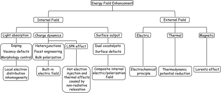
The internal electric and thermal fields within materials and applied external energy fields (e.g., thermal, electric, and magnetic fields) can significantly affect the behaviour of photo-excited charge carriers in catalysts and catalytic throughput.21–24 As implied by the description of heterojunctions above, internal electric fields typically arise from the polarization of uneven charge distributions across various component layers,25 and numerous studies have focused on heterojunction-type internal electric fields to influence the dynamic behaviour of photogenerated excitons and improve the performance of POWS. For instance, Takata et al. enhanced the distribution of electric fields within a crystal by selectively depositing separate co-catalysts for the hydrogen and oxygen evolution reactions on different crystal facets of a modified Al-doped strontium titanate semiconductor photocatalyst, resulting in an enhanced rate of forward (productive) charge transfer events and achieving an internal quantum efficiency approaching unity.26 Similarly, albeit through a physical mechanism rather than an intrinsic change in materials structure through introduction of different heterojunctions, Li et al. demonstrated effective seawater splitting using N-doped TiO2 with selective accumulation of electrolyte ions of opposite charge from the reaction medium on different photopolarized crystal facets, thereby and prolonging the charge-carrier lifetime by a factor of five.27
Moreover, strategies aiming at modulating the band structure of semiconductors, such as doping or introduction of defects, have recently been shown to create non-centrosymmetric structures within semiconductor catalysts, thereby inducing spontaneous polarization and generating internal electric fields.28 A notable example is the work reported by Li et al., who doped carbon into Bi3O4Cl nanosheets, resulting in a 126-fold enhancement of its internal electric field and achieving a bulk charge separation efficiency of 80%.29 Analogous to the effect of doping that leads to uneven local electron distributions, defects can also disrupt or alter the perfect periodic arrangement of atoms or molecules in crystalline materials, thereby modifying the local electronic states or space charge regions in response to changes in the internal electric field.30
Furthermore, traditional morphology control strategies aiming at enhancing the light-harvesting capabilities of photocatalysts have recently been shown to significantly facilitate internal field enhancement, with the tip effect being the most frequently documented phenomenon.31 The tip effect pertains to the concentration of energy forms, including electrons, photons, and magnetic fields, at regions of high curvature, which results in the amplification of local electric, thermal, and magnetic fields.32 This phenomenon is also referred to the “wrinkle” effect in semiconductor nanomaterials, and which will be elaborated upon in subsequent sections of this review. Notably, the wrinkle effect is most prominently observed in metallic nanomaterials, commonly recognized as the localized surface plasmon resonance (LSPR) enhancement effect.33 Intriguingly, the LSPR effect in metals not only contributes to the enhancement of the local internal electric field but is also associated with a thermal effect that can elevate local temperatures, thereby enhancing the apparent activity of the catalyst to a certain degree.34 For instance, Ha et al. illustrated that hot electrons produced by Au nanorods can be effectively transferred to TiO2 situated at the tips of the nanorods for the purposes of storage and utilization. This process is facilitated by the LSPR effect of the Au nanorods, resulting in selective photoreduction and photooxidation of water occurring at the tip TiO2 and the sides of the Au nanorods, respectively.35
In the context of external field-assisted POWS, the mechanism of field enhancement is particularly well-defined, especially concerning external electric and magnetic fields. POWS technology is rooted in photoelectrochemical reactions, where the mechanism of the external electric field aligns with that of traditional electrochemical reactions, while the influence of the magnetic field primarily draws upon the Lorentz effect.19 Both mechanisms play a significant role in the overall directional separation of macroscopic carriers. In contrast, the impact of the external thermal field on carrier dynamics remains a subject of debate. One perspective posits that lattice vibrations induced by temperature increases can lead to electron-phonon scattering.36 However, in the case of thermodynamically uphill reactions such as water splitting, a macroscopic increase in temperature is likely to result in a reduction of the reaction barrier. Consequently, modulation of these energy fields becomes crucial for optimizing the energy consumption, improving the light utilization efficiency, and promoting the hydrogen production. This approach is thus promising in harnessing full-spectrum sunlight for scalable green hydrogen generation.
There are a number of excellent review articles that address various of these aspects of the POWS. For instance, Sun et al. have detailed the advantages of metal–organic frameworks (MOFs) as modularly assembled solids that allow elucidation of several of the structure–performance relationships that are important in POWS and CO2 reduction.37 Zhao et al. have reviewed transition metal-based co-catalysts for water splitting in recent years,38 while Tao et al. have highlighted materials design strategies to increase the charge separation within particulate photocatalysts, including the introduction of surface junctions, spatial charge separation between facets, and polarity-induced charge separation.39 Li et al. have described and summarised the effects of external thermal gradients, magnetic fields, microwave radiation and ultrasound waves on a variety of photocatalysts and the impact on the reactions that they promote.23 However, the effects of band structure, morphology control, heterojunctions, surface/interface modification and the range of external fields and stimuli on the internal charge generation, transport and surface chemistry of the photocatalysts that promote the POWS have not been thoroughly reviewed, despite the insight that such a collated description would provide for future catalyst designs.
In this review, we first discuss the challenges of POWS from three perspectives: thermodynamics; charge carrier generation and transport; and macroscopic reaction kinetics. On this basis, the corresponding solutions are proposed from three fundamental aspects: material composition and structure; internal fields; and the application of external stimuli. Specifically, the review focuses on the different types of semiconductor materials that have been applied as photocatalysts for the POWS, with the effects of the semiconductor bandgap, and the mainstream catalyst modification strategies on the photoexciton generation and transport, and the chemical aspects of the overall water splitting reaction mediated at the surface. The impact of these higher-level concepts is interpreted from the perspective of the internal intrinsic electric/polarization field within these materials and the influence of an applied external field. The effects of different reaction types on the reaction kinetics of different materials are also summarized and discussed. Finally, the limitations of contemporary POWS systems are summarized, and directions for future development are proposed.
2. Fundamentals and challenges of POWS
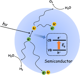
The POWS reaction on a semiconductor photocatalyst can be broadly considered in terms of three general processes (Fig. 1).40 Impact of light of energy greater than the semiconductor bandgap (Eg) results in promotion of an electron from the top of the valence band (VB) to the conduction band (CB). The resulting hole in the VB (h+) and electron in the CB (e−) can recombine in the bulk, with the net result that the absorbed light energy has simply been converted into heat energy, or emitted as a photon of lower energy through fluorescence. If the photogenerated charges diffuse away from each other before recombination, the resulting charge separated pair may migrate to the surface where they may again recombine or promote the coupled reduction and oxidation steps necessary to achieve the overall water splitting reaction to give H2 and O2.41However, beneath these elementary descriptive steps, the POWS combines very complex physical and chemical process, which brings about great challenges to achieve high efficiencies. The common problem of a high carrier recombination rate within the bulk is compounded by the surface state and environment that strongly influence charge recombination at the photocatalyst surface.42 Further complicating the model, the processes of charge separation, migration and the surface reactions with substrates cannot be independently optimised as they are inherently related to each other.43 In other words, the imbalance between the rate of charge migration to the rate of the chemical steps involved in the reaction at which take place at sites on the surface with specific structure governed by the nature of the reactants and products will also lead to a low overall reaction efficiency.
In addition, in thermodynamic terms, the splitting of water into H2 and O2 in an electrolytic cell is an energy-consuming reaction, theoretically requiring 1.23 eV (ΔG = + 237 kJ mol−1) of energy (eqn (1)) based on the redox potential of the water splitting reaction (H+/H2, 0 V and O2/H2O, 1.23 V vs. normal hydrogen electrode at pH = 0).44 In contrast, the direct reverse reaction, i.e., the combination of H2 and O2 to reform water, is highly exothermic and more thermodynamically favourable than the POWS reaction.45 Therefore, many studies have introduced sacrificial redox agents into the reaction system to quench either the hydrogen evolution reaction (HER) or oxygen evolution reaction (OER) and avoid the recombination of H2 and O2 products. However, these sacrificial half-reactions, which are thermodynamically downhill processes, are accompanied by a reduction in Gibbs free energy, resulting in a waste of photon energy.46 Developing photocatalysts that do not require these reagents to achieve productive overall water splitting remains a great challenge.
| 2H2O → 2H2 + O2, ΔG = +237 kJ mol−1 | (1) |
The POWS process is also governed by carrier dynamics. The generation, separation, and migration of photogenerated charges to the catalyst surface occur on the timescale of femtoseconds to nanoseconds, while the subsequent redox reactions on the surface take much longer (microseconds to seconds)47 and are generally considered the rate-limiting step of the entire photocatalytic reaction. Since the effective amount of photogenerated h+ is larger than that of e−,48 the migration rates of the two in the catalyst bulk are also different, leading to the incompatibility of the OER and HER reaction rates. In addition, the larger overpotential of the OER relative to the HER and the greater affinity of O2 for most catalyst surfaces49 results in a greater thermodynamic driving force to promote the OER.
Therefore, it can conclude that the current challenges facing POWS mainly lie in the following three areas:
(a) The thermodynamic limitation of POWS reaction, that is, the endothermic nature of the forward reaction and reverse exothermic characteristics, hinders the coexistence of H2 and O2, and poses a challenge to the redox potential of semiconductor catalysts, indicating that the development of photocatalysts with high excited state redox potentials necessary to overcome the overpotentials and provide the net driving force for the reaction is still a research theme in this field.
(b) The incompatibility between the separation and transport of photogenerated carriers within the bulk and the facile charge recombination reactions on semiconductors surfaces are among the main reasons for the low efficiency of the POWS reaction. Internal field enhancement combined with surface modification can be an effective means to improve charge separation whilst increasing the dispersion and randomness of surface reactions, thereby reducing carrier pair self-annihilation.
(c) The macroscopic kinetics of the charge carriers is a core limitation to the surface-catalysed reactions, due to the longer time associated with photoexcitons acting on reactants compared to the microscopic separation and migration processes. The apparent reaction rate and mass transfer efficiency can be improved by upgrading the reaction system to improve the surface catalytic response, with assistance from the application of an external field.
3. Basic material principles for POWS
3.1 Host semiconductor nanomaterials
In order to realize the simultaneous occurrence of the electron-driven water reduction reaction and the hole-driven water oxidation reaction, the band edge positions of a semiconductor are critical. Effective reaction requires the reduction electrode potential and oxidation electrode potential of water fall within the VB and CB potentials of the semiconductor (Fig. 2A), ensuring that the potential of the conduction band minimum (CBM) where the photogenerated e− are located is more negative than the H+/H2 energy level (0 V, eqn (2)), and the potential of the valence band maximum (VBM) where the photogenerated h+ are located is more positive than the O2/H2O energy level (1.23 V, eqn (3)).39 In addition to the band edge positions, Eg is another important parameter that shapes the activity of a semiconductor, because the bandgap width of the semiconductor determines its light absorption threshold and directly affects its utilization of light energy. The wavelength range of solar spectrum that can be observed on the Earth is 295–2500 nm,54 of which infrared light accounts for about 53%, visible light for about 44%, and ultraviolet light only for about 3% (Fig. 2B).50 Therefore, the semiconductor band gap should be theoretically less than 3.0 eV to improve the utilization of the visible light (>400 nm), according to the relationship (eqn (4)) between the semiconductor band gap and light absorption.55| 2H+ + 2e− → H2, E = 0 V | (2) |
| 2H2O + 4h+ → 4H+ + O2, E = 1.23 V | (3) |
| αhv = (hv − Eg)n where n = 1 or 1/2 | (4) |
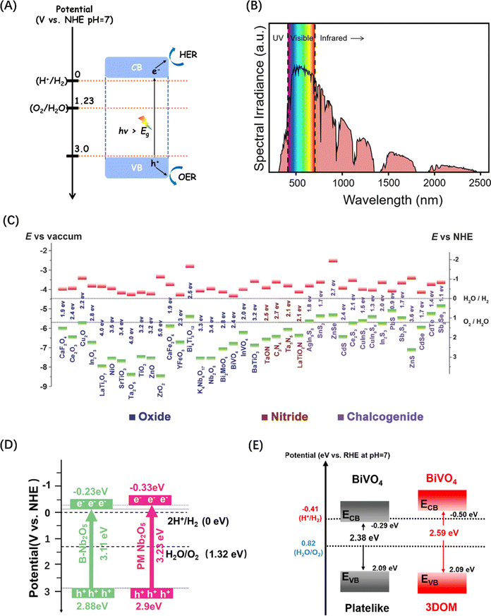 | ||
| Fig. 2 (A) Schematic energy level diagram of the POWS reaction of semiconductor photocatalysts. (B) Standard solar radiation spectrum at the Earth surface at sea level. Reproduced from ref. 50 with permission from American Chemical Society, copyright 2022. (C) Band structure comparison of metal oxides commonly used in POWS. Reproduced from ref. 51 with permission from John Wiley and Sons, copyright 2015. (D) Energy band structure diagrams for two types of Nb2O5. Reproduced from ref. 52 with permission from John Wiley and Sons, copyright 2024. (E) Energy band structure diagrams for two types of BiVO4. Reproduced from ref. 53 with permission from American Chemical Society, copyright 2021. | ||
Semiconductor-based photocatalytic water splitting technology was developed in early 1970s, marked by the discovery of the process on a TiO2 semiconductor single crystal electrode.2 Since then, a variety of photocatalysts have been studied and reported. The general principle demonstrated by these photocatalysts is that metal cations with one of two specific electronic structures are active in POWS: transition metal cations with a d0 electron configuration (such as Ti4+, Zr4+, Nb5+, Ta5+, and W6+), and typical metal cations with d10 electron configuration (such as Ga3+, In3+, Ge4+, Sn4+, and Sb5+), while the CBM of the corresponding oxide is mainly contributed by the empty d or sp orbital of the metal cation.45,46 Since the VBM consisting of O2p orbitals lies at about 3 V (relative to normal hydrogen electrode (NHE) at pH = 0),46 then as long as the potential of the CBM is less than zero (more negative than the H+/H2 energy level), the bandgap energy of these oxides will be higher than 3 eV. As a result, both d0-type and d10-type oxides tend to exhibit POWS activity (Fig. 2C).51 Recent studies have indicated that the band energies of traditional metal oxide semiconductor materials like Nb2O5 (ref. 52) and BiVO4 (ref. 53) can be tuned by changes to the macroscopic structure, leading to an increased potential for POWS, as shown in Fig. 2(D) and (E). However, the high potential of VB formed by the O2p orbital makes the Eg theoretically at least 3 eV. However, such band gaps limit the light required to drive POWS activity to the near-ultraviolet range, with no response to visible and near-infrared light, which together account for about 97% of the solar spectrum energy.
To improve the visible light response of photocatalyst candidates, semiconductors with VBM between +1.23 and +3 V have attracted extensive attention. Since N is less electronegative than O, the N2p orbital of metal nitrides form VBs at a less positive potentials than the VBs generated by the O2p orbital in oxides, while the potential of CB is almost unaffected by the introduction of nitrogen.56 The crystal and energy band structure of a series of Ta–O–N functional materials have been studied through theoretical calculations, showing that the band gap energy of ε-Ta2O5, TaON and Ta3N5 gradually decreases (Fig. 3A), confirming that nitrogen can raise and widen the valence band of Ta–O–N materials.57 Polycrystalline Ta3N5 nanorods with an optimized morphology and crystallization properties attaining near-ideal water splitting with a Faraday efficiency of nearly 100% have also been described (Fig. 3B).58 Additionally, metal nitride materials such as Ge3N4,66 GaN,67 and InGaN (Fig. 3C)59 have also been proven to be efficient in the POWS process.
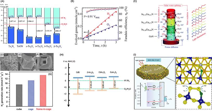 | ||
Fig. 3 (A) Band diagrams for Ta2O5, TaON, and Ta3N5. Reproduced from ref. 57 with permission from Royal Society of Chemistry, copyright 2018. (B) Stoichiometric 2![[thin space (1/6-em)]](https://www.rsc.org/images/entities/char_2009.gif) : :![[thin space (1/6-em)]](https://www.rsc.org/images/entities/char_2009.gif) 1 evolution of hydrogen and oxygen gases on polycrystalline Ta3N5 nanorods. Reproduced from ref. 58 with permission from American Chemical Society, copyright 2023. (C) Schematic diagram of POWS process occurring on InxGa1−xN four-band nanowires. Reproduced from ref. 59 with permission from Royal Society of Chemistry, copyright 2019. FESEM images of Cd cubes (D), cage (E), and frame-in-cage (F). (G) Comparison of photocatalytic H2 generation rates of CdS nanoparticles with three morphologies. (D–G) Reproduced from ref. 60 with permission from John Wiley and Sons, copyright 2020. (H) Band diagrams for CdS (adapted from ref. 61 with permission from Royal Society of Chemistry, copyright 2019), ZnIn2S4 (adapted from ref. 62 with permission from John Wiley and Sons, copyright 2021), CdIn2S4 (adapted from ref. 63 with permission from John Wiley and Sons, copyright 2022), and CoIn2S4 (adapted from ref. 64 with permission from Elsevier, copyright 2024). (I) Operational mechanism of POWS on DO-ZIS. Reproduced from ref. 65 with permission from Springer Nature, copyright 2024. 1 evolution of hydrogen and oxygen gases on polycrystalline Ta3N5 nanorods. Reproduced from ref. 58 with permission from American Chemical Society, copyright 2023. (C) Schematic diagram of POWS process occurring on InxGa1−xN four-band nanowires. Reproduced from ref. 59 with permission from Royal Society of Chemistry, copyright 2019. FESEM images of Cd cubes (D), cage (E), and frame-in-cage (F). (G) Comparison of photocatalytic H2 generation rates of CdS nanoparticles with three morphologies. (D–G) Reproduced from ref. 60 with permission from John Wiley and Sons, copyright 2020. (H) Band diagrams for CdS (adapted from ref. 61 with permission from Royal Society of Chemistry, copyright 2019), ZnIn2S4 (adapted from ref. 62 with permission from John Wiley and Sons, copyright 2021), CdIn2S4 (adapted from ref. 63 with permission from John Wiley and Sons, copyright 2022), and CoIn2S4 (adapted from ref. 64 with permission from Elsevier, copyright 2024). (I) Operational mechanism of POWS on DO-ZIS. Reproduced from ref. 65 with permission from Springer Nature, copyright 2024. | ||
Apart from nitrides, metal chalcogenides, and particularly metal sulfides, are also favourable candidates as visible light-driven photocatalysts because their VBs typically comprise the p orbitals of S, which have shallower energy levels than that of O2p orbitals.68 The most studied metal sulphide semiconductors are ZnS and CdS, between which ZnS has a wide band gap, i.e., 3.6 eV at room temperature.69 In contrast, the bandgap energy of CdS is only 2.4 eV,61 endowing effective utilization of visible light. An interesting study synthesized three nanostructured forms of CdS materials (Fig. 3D–F) featuring and combining the thin-shell, hollow and frame-like structures that enhance light absorption, minimize distances for the transfer of photogenerated charges to the active surface, and enhance mass transport and explored their POWS potential. These studies confirmed that CdS frame cage particles have supreme activity compared to cubes and cages, with the highest H2 generation rate (Fig. 3G).60 Additionally, ternary metal sulphides have also attracted much attention because of their higher chemical and photostability than binary metal sulphides. For example, ZnIn2S4,62 CdIn2S4,63 and CoIn2S4,64 have been developed as photocatalysts with efficient visible light response capabilities (Fig. 3H). However, it is still difficult for metal sulphides to completely split H2O into H2 and O2 without carrier sacrificial agents, because S2− in the material can be easily oxidized by h+ near the VBM, resulting in self-photocorrosion without the release of O2.70 Nevertheless, Chong et al.71 synthesized a superhydrophilic ZnIn2S4 that can drive photocatalytic pure water splitting and maintain near uniform stability and performance throughout the daytime reaction. It was also confirmed that the charge redistribution caused by defects enhances the activation of water and reduces the surface dynamic barrier. Xin et al.65 reported a cationic oxygen-doped ZnIn2S4 (DO-ZIS) induced by lattice distortion and found that the electron-rich S1 site in the local structure S1–S2–O site is favourable for hydrogen adsorption, while the strong charge redistribution property activates a stable oxygen reaction at the electron-deficient S2 site, which can avoid the sulphur instability problem common in metal sulphide photocatalysis (Fig. 3I).
Metal halide perovskite (MHP) materials are ionic crystals with a general chemical formula ABX3, in which A site is usually a monovalent cation or ionic group, and B site is a transition metal ion, which ensures that it has a negative CBM.72 Generally, the VB band edge of MHP materials can usually be adjusted by the halide anion at the X position (Fig. 4A).73 For example, it has been reported that Ba2Bi3Nb2O11I is not only responsive to a wider range of visible light than chlorides and bromides, but also acts as a stable photocatalyst and can effectively oxidize water (Fig. 4B).74 In addition, Wang et al. synthesized a perovskite solid solution photocatalyst, La1−xCaxTaO1+yN2−y (0 ≤ x, y ≤ 1), which also achieved the purpose of regulating the band edge of MHP materials by regulating the ratio of two ions at the A-position (Fig. 4C).75 It is worth mentioning that MHP-based solar cells have demonstrated an efficiency higher than 25%,77 which makes them an extremely popular material for both solar energy harvesting and photocatalyst research in recent years. Inspired by the structure of perovskite solar cells, an MHP-based photoelectrode system was constructed for water splitting in alkaline electrolytes.78 On this basis, improved photoelectrode structures, such as p-type-intrinsic-n-type (p-i-n)79 and n-i-p80 structures, have also appeared and demonstrated excellent performances. It should be noted that a key reason for introducing MHP materials to electrode structures is that designing perovskite-metal heterostructures is not simple, because noble metal nanoparticles loaded on the surface of MHP nanocrystals tend to agglomerate under steady-state illumination, leading to the loss of noble metal nanostructures and thus affecting the catalytic activity. Despite the widespread adoption of electrode systems, the soft nature of MHPs makes them susceptible to surface transformation or degradation in electrolyte systems.81 Therefore, it is particularly important to introduce photoelectrode protection measures while avoiding affecting the mass transfer efficiency. It is exciting to note that Fehr et al. designed a halide perovskite-based photochemical cell composed of silicon perovskite monolayers stacked in series, with a peak STH efficiency of 20.8%, and continuous operation for 102 h under AM 1.5 G illumination, showing a new possibility for the development of productive, durable, and competitive solar water splitting technology, as shown in Fig. 4(D) and (E).76
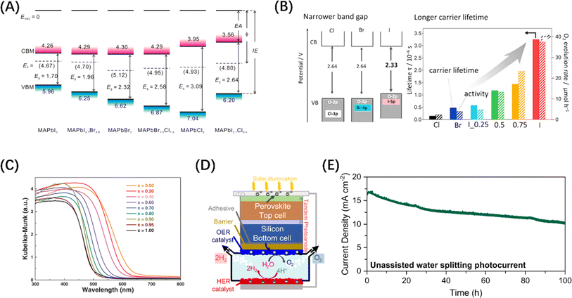 | ||
| Fig. 4 (A) Changes in the energy band levels of MAPbX3 after substitution of the X position. Reproduced from ref. 73 with permission from American Chemical Society, copyright 2016. (B) Comparison of the band structures of three types of Ba2Bi3Nb2O11X and the O2 evolution rate over them. Reproduced from ref. 74 with permission from American Chemical Society, copyright 2021. (C) UV-vis diffuse reflectance spectroscopy of La1−xCaxTaO1+yN2−y (0 ≤ x, y ≤ 1). Reproduced from ref. 75 with permission from John Wiley and Sons, copyright 2020. (D) Schematic diagram of the structure of Si/perovskite composite photochemical cell. (E) 2-Electrode unassisted water-splitting over time in Si/perovskite hybrid photochemical cell. (D and E) Reproduced from ref. 76 with permission from Springer Nature, copyright 2023. | ||
Conjugated polymer nanomaterials (i.e. organic semiconductors) have emerged as promising candidates for water splitting in recent years because of their delocalized π-systems and diverse synthetic modularity, which allow them to absorb visible light and to systematically control the electronic and structural properties.82,83 In particular, conjugated polymer nanophotocatalysts received more attention after graphitic carbon nitride (g-C3N4) was demonstrated to be an excellent photocatalyst for visible-light-driven H2 production.84 For example, graphene,85 C2N86 and Ni(OH)2 (ref. 87) modified g-C3N4 have been demonstrated as visible light responsive photocatalysts, as shown in Fig. 5A–C. DFT studies showed that the CB and VB positions of g-C3N4 are −1.12 and +1.57 V, respectively.84 Similarly, the band gap of g-C3N4 can be tuned by doping more N in the CN skeleton. Mesoporous carbon nitrides with C3N5 (ref. 91) and C3N6 (ref. 92) stoichiometry have been reported to have narrower band gap width than C3N4. The C/N ratio in carbon nitride can also be controlled by changing the calcination temperature, and hence tune the band gap (Fig. 5D).88 However, the OER yield of g-C3N4-based metal-free photocatalysts is very low and further work is required to design POWS photocatalysts based on these materials.82 For example, Ai et al.89 synthesized a P-doped g-C3N4/Ti3C2 composite material (PCNT-3-5), on which the O2 evolution rate can be as high as 1527.3 μmol g−1, while pristine g-C3N4 (CN) was not active, as shown in Fig. 5(E). The boosted activity of the complex was ascribed to the construction of heterojunction rather than the improvement of OER activity of g-C3N4 itself. Chen et al. demonstrated that the overall downshifting of the energy band caused by protonation can increase the thermodynamic driving force of g-C3N4, but a sacrificial redox agent is required in the reaction medium (Fig. 5F).90 It concludes that the downward shift requirement of VB and the dependence on sacrificial agents limit the photocatalytic ability of this type of photocatalyst towards POWS.
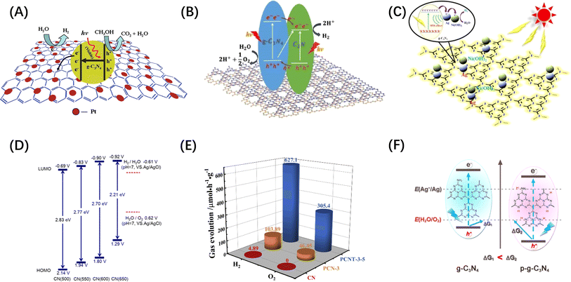 | ||
| Fig. 5 (A) Electron separation and migration enhancement mechanism in graphene/g-C3N4 composites. Reproduced from ref. 85 with permission from American Chemical Society, copyright 2011. (B) Possible pathways for electron–hole separation in g-C3N4/C2N nanocomposite. Reproduced from ref. 86 with permission from John Wiley and Sons, copyright 2016. (C) Proposed photocatalytic hydrogen production mechanism over Ag/Ni(OH)2/g-C3N4 photocatalyst. Reproduced from ref. 87 with permission from John Wiley and Sons, copyright 2022. (D) Electronic band structure of C3N4 after heat treatment at different temperatures. Reproduced from ref. 88 with permission from American Chemical Society, copyright 2018. (E) Comparison of POWS products release rates of CN, PCN-3 (P-doped g-C3N4) and PCNT-3-5. Reproduced from ref. 89 with permission from Elsevier, copyright 2019. (F) Energy band comparison of g-C3N4 before and after protonation treatment. Reproduced from ref. 90 with permission from American Chemical Society, copyright 2015. | ||
In addition to the above-mentioned two-dimensional (2D) planar materials, those with a three-dimensional (3D) network topology, such as MOFs and covalent–organic frameworks (COFs) materials, have also been developed as photocatalysts with POWS activity. MOFs utilize coordination chemistry as the driving force to assemble organic or organometallic linkers around metal secondary structural units to form coordination polymers with clear topological structures.50,93,94 COFs are periodically arranged porous organic polymers, which are crosslinked into regular structures by linking organic building blocks connected through covalent bonds.95,96 Although MOFs and COFs were initially and widely used in gas adsorption and separation because of their macroporous structures and large surface areas, they can both exhibit visible light photocatalytic activity after energy band adjustment. For MOFs materials, the adsorption properties can be tuned by changing the organic ligands, and UiO66(Zr)-X (X = –H, –NH2, –NO2, and –Br) is a good example (Fig. 6A).97 The band gap control of COFs can be achieved by rationally adjusting the building blocks and introducing electron donor–acceptor (D–A) units and π-conjugated systems, such as skeleton group reactions and bulk phase integration and stripping strategies (Fig. 6B).96,98 It should be noted that MOF- and COF-based materials have a low carrier mobility and high recombination rate due to the organic linking groups and porous structures, limiting their widespread acceptance. Therefore, the introduction of co-catalyst particles is an indispensable step for enabling these two materials to be effective in POWS, aiming to transfer the traditional catalytic reaction sites from the surface to the interior of the catalyst. This not only spatially separates the carriers but also avoids the recombination of carriers during long-distance transport, as shown in Fig. 6(C) and (D).99,100 In contrast to inorganic materials, organic materials exhibit a low dielectric constant and weak non-covalent electronic interactions, which result in the formation of electrostatically bound excitons upon photoexcitation.101 For these excitons being effectively utilized as a current or to initiate redox reactions, they must dissociate into free charge carriers within their lifetime. The strength of the electrostatic binding energy of the electron–hole pair is influenced by the magnitude of the Coulomb interaction between the excitons.102 From an energy perspective, the strategy of additive modification in organic semiconductor systems aims to enhance the dissociation of excitons by manipulating the energy difference between the charge transfer states of the donor and acceptor components.103 Consequently, a significant energy difference between the donor and acceptor is highly desirable, akin to the operational mechanism of the built-in electric field present in Schottky heterojunctions in inorganic semiconductors.
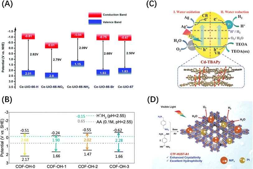 | ||
| Fig. 6 (A) Band structure diagram of UiO66(Zr)-X. Reproduced from ref. 97 with permission from John Wiley and Sons, copyright 2019. (B) Band positions and band gaps of COFs with different numbers of –OH. Reproduced from ref. 98 with permission from Royal Society of Chemistry, copyright 2022. (C) Mechanism diagram of visible light-driven POWS products release on Pt and CoPi co-modified Cd-based MOF. Reproduced from ref. 99 with permission from John Wiley and Sons, copyright 2018. (D) Mechanism diagram of visible-driven POWS on the covalent triazine frameworks (CTFs) co-deposited by Pt and NiPx. Reproduced from ref. 100 with permission from John Wiley and Sons, copyright 2020. | ||
3.2 Co-catalysts for hydrogen reduction
While the various semiconductor materials mentioned above have the potential of serving as POWS catalysts, the high carrier recombination rate in the bulk and inefficient surface reactions greatly limit their applications. Especially for the OER reactions, most of the above-mentioned single host catalysts do not have the ability to completely split water to stoichiometrically generate H2 and O2, because there is a certain difficulty in balancing the band gap width and forming a sufficiently positive VBM. However, it has been proven that modifying the catalyst surface with co-catalysts tailored towards HER and OER activity can significantly improve the POWS performance.38,104The most reported HER co-catalysts are metals and their alloys, especially coinage metals, such as Cu, Au, Ag, Pt, etc.38 The work functions of these metals are generally large, thus after the metals contact with a semiconductor, the e− on the semiconductor CB spontaneously migrates to the noble metal until the Fermi levels of the two sides of the heterojunction are balanced. At the same time, the h+ remains in VB, resulting in the bending of the semiconductor's energy band and the formation of a space charge region, which is responsible for the formation of the Schottky barrier, as shown in Fig. 7(A) and (B).105 For such a configuration, the metal can function as an electron trap to separate carriers, thus contributing to the improved photocatalytic activity. On this basis, an alloy co-catalyst formed by assembling two metals with different Fermi levels has a greater charge separation efficiency than a single metal, resulting in a synergistic effect of the two. Metal alloys, such as AuPd,112 NiMo,113 and NiCo,114 have been reported as photocatalysts for the HER. Similarly, carbon-based materials, such as carbon quantum dots,115 carbon nanotubes (Fig. 7C),106 graphene,116 and other carbon-based materials are frequently used to modify semiconductor base materials to enhance the HER activity because of their good conductivity and electron storage capabilities. It is worth mentioning that metal borides and metal nitrides can also integrate Schottky junctions in contact with semiconductors due to their metal-like properties.38 For example, VB2,117 MoB (Fig. 7D),107 NbN,118 and MoN (Fig. 7E)108 have been demonstrated to promote the transfer of photogenerated electrons in CdS and increase the evolution of H2; meanwhile, some co-catalysts can also enhance the stability of CdS. In addition, transition metal phosphides, such as FeP,119 CoP (Fig. 7F),109 Ni2P,120 and Cu3P,121 have been developed for photocatalytic HER, because of the “ensemble effect”. The P atoms in these phosphides have modest bonding strength to hydrogen, which facilitates the formation of H2 molecules while reducing the H-poisoning effect.122 Transition metal sulphides have also been extensively exploited as co-catalysts for photocatalytic HER due to their admirable surface properties which are well suited to the surface binding of both water molecules and H protons and their effective activity in boosting photogenerated exciton separation.38 Quantum dot (QD) materials, such as MoS2 (Fig. 7G),110 Co3S4,123 NiS2,124 and CuInS2 (ref. 125) show higher photocatalytic HER activity, particularly when smaller QD are employed. Some transition metal oxides, after reducing their size, can also serve as HER sites. Taking the TiO2 host catalyst as an example, CuO (Fig. 7H),111 Cu2O,126 and CoO127 can all be used as co-catalysts to foster the spatial separation of photogenerated carriers. Similarly, transition metal hydroxides such as Ni(OH)2 (ref. 128) and Cu(OH)2 (ref. 129) can also form heterojunctions with semiconductors to suppress the self-coupling of photogenerated carriers.
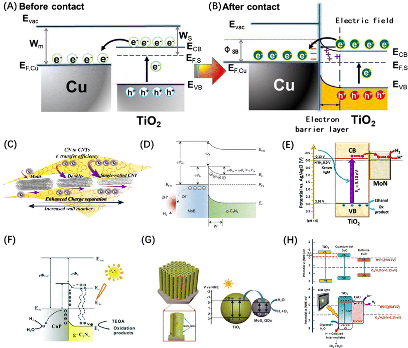 | ||
| Fig. 7 The change of energy band before (A) and after (B) contact between Cu and TiO2 and the migration path of photogenerated carriers. (A and B) Reproduced from ref. 105 with permission from Elsevier, copyright 2019. (C) Schematic diagram of photogenerated excitons to carbon nanotubes in g-C3N4. Reproduced from ref. 106 with permission from Elsevier, copyright 2018. (D) Schematic diagram of Schottky junction formed by MoB in contact with g-C3N4. Reproduced from ref. 107 with permission from John Wiley and Sons, copyright 2018. (E) The exciton dissociation and migration in the MoN/TiO2 system. Reproduced from ref. 108 with permission from Royal Society of Chemistry, copyright 2018. (F) Schematic diagram of the Schottky contact on CoP/g-C3N4. Reproduced from ref. 109 with permission from Royal Society of Chemistry, copyright 2018. (G) Energy band structure and charge transfer mechanism of MoS2@TiO2 heterostructure. Reproduced from ref. 110 with permission from John Wiley and Sons, copyright 2018. (H) Reaction mechanism diagram of photocatalytic water splitting over CuO–TiO2 nanocomposites. Reproduced from ref. 111 with permission from American Chemical Society, copyright 2018. | ||
3.3 Co-catalysts for water oxidation
Since the OER process consumes four h+ per two water molecules and is slower than the HER process, the function of the co-catalyst for H2O oxidation mainly involves two aspects: accelerating the transfer of h+ to the surface-active sites; and reducing the overpotential of the OER. Although metal co-catalysts can serve as e− potential traps to promote the HER reactions and improve the OER activity to a certain extent, this indirect effect is limited by the lack of high-flux carrier catalytic sites. To address this problem, some hydrophilic hydroxides (Co(OH)2,130 Fe(OH)3 (Fig. 8A),131 Ni(OH)2,136etc.) or hydroxyl hydroxides (CoOOH (Fig. 8B)132 and FeOOH137) have been identified as ideal OER co-catalyst candidates. The VB potential of these co-catalysts is usually more negative than that of the host semiconductor. Therefore, h+ tends to migrate from the VB of the host semiconductor to the VB of the co-catalyst when the two materials are brought into contact, causing the energy band to bend to form a h+ barrier. There are also some transition metal oxides (CoOx (Fig. 8C),133 MnOx,138 NiCo2O4,139etc.) used as HER co-catalysts that can also enhance OER if the VB is compatible with the host semiconductors. Of course, if the CBM of the co-catalyst is simultaneously more negative than that of the host semiconductor, the photogenerated carriers will be spatially separated to the greatest extent. It is worth mentioning that the physical size of co-catalyst is generally on the nanoscale, and the co-catalyst particles are highly dispersed over the bulk semiconductor, which ensures the formation of high-flux and high-density catalytic sites. In addition, some single-atom metals, such as Co (Fig. 8D and E)134,135 and Fe,140 can also enhance the OER activity. Different from the mechanism of metal enhancing the HER activity of host semiconductors, single-atom metals can form surface unsaturated coordination by combining with or replacing host atoms to form catalytic active sites.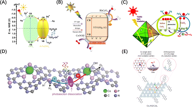 | ||
| Fig. 8 (A) Energy level comparison and carrier migration path diagram of CeO2/Fe(OH)3 heterostructure. Reproduced from ref. 131 with permission from John Wiley and Sons, copyright 2021. (B) Mechanism diagram of photothermal catalytic water splitting over SrTiO3 loaded with RhCrOx/CoOOH. Reproduced from ref. 132 with permission from Elsevier, copyright 2024. (C) Mechanism diagram of photocatalytic water splitting over CoOx-loaded CeO2 composite. Reproduced from ref. 133 with permission from Royal Society of Chemistry, copyright 2017. (D) Schematic diagram of POWS on Co–P-modified g-C3N4 photocatalyst. Reproduced from ref. 134 with permission from John Wiley and Sons, copyright 2017. (E) Schematic diagram of the redox sites on anthraquinone-loaded g-C3N4 embedded with Co single atoms. Reproduced from ref. 135 with permission from PNAS, copyright 2020. | ||
4. Field promotion behind catalyst modification strategies
While co-catalyst modification can improve the surface reaction of a catalyst to a certain extent, the trace nature of the co-catalytic sites often results in limited promotion of the POWS process. Therefore, it is necessary to synchronize other intrinsic modification strategies, such as the manipulation of internal structure and energy fields to improve light absorption capabilities, enhancement of carrier dynamics, and promotion of charge output.36 In the sections that follow, the mechanisms of these energy field modifications are analysed from the perspective of improvements in these properties.4.1 Light absorption enhancement
Metal doping is a successful strategy for enhancing the spectral sensitivity of semiconductor photocatalysts possessing wide bandgap properties. The incorporation of metal cations possessing ionic radii comparable to those of the host ions may diminish the impetus for electronic transitions by either engaging with the VB or CB, or by creating energy levels within the band gap,142 which can change the physical properties of the intrinsic semiconductor so that it has p/n characteristics, as shown in the Fig. 9(A). Various metal ions, such as V4+, Cr3+, Mn3+, Fe3+, and Ni2+, were introduced into TiO2 to promote OER and/or HER reactions under visible light irradiations.149 A similar strategy of enhancing water splitting performance by metal doping was also demonstrated in a study of SrTiO3 material, as shown in Fig. 9(D).143 Combined with relevant computational studies, the optical response shift after doping is related to the ionic radius of the dopant. The change in the absorption edge typically rises as the cation radius decreases, while the energy states of impurities tend to shift towards lower energy levels as the atomic number of the dopant increases.150
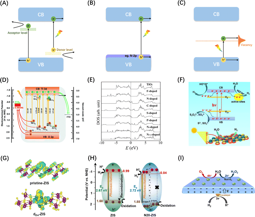 | ||
| Fig. 9 Schematic diagram of semiconductor energy band engineering: (A) metal doping; (B) non-metal element doping; (C) vacancy engineering. (D) Comparison of energy bands of SiTiO3 doped with different metal elements. Reproduced from ref. 143 with permission from Royal Society of Chemistry, copyright 2018. (E) Densities of states (DOSs) of the substitutional doping of C, N, F, P, or S for O in the anatase TiO2 crystal. Adapted from ref. 144 with permission from The American Association for the Advancement of Science, copyright 2001. (F) Diagram of photocatalytic water splitting and charge transfer mechanism in ZnS with abundant surface vacancy defects under sunlight irradiations. Reproduced from ref. 145 with permission from American Chemical Society, copyright 2021. (G) Differential charge density maps of the primordial-ZIS atomic layer and the dZni-ZIS atomic layer. Reproduced from ref. 146 with permission from Elsevier, copyright 2022. (H) Schematic diagram of band structure and corresponding photoinduced activity of original ZIS and N-doped ZIS samples. Reproduced from ref. 147 with permission from Elsevier, copyright 2023. (I) Diagram of charge separation mechanism between different crystal faces of PbTiO3 caused by oxygen vacancy. Reproduced from ref. 148 with permission from American Chemical Society, copyright 2022. | ||
Unlike metal doping that introduces interband energy states, doping by introducing a trace amount of non-metallic N, C, S, or halogen (F, Cl, Br) into the semiconductor structure generally reduces the band gap by increasing the VB edge (Fig. 9B).151 Since Np orbitals are well suited to mix with O2p and the ionic radii of the two elements are similar, N doping is most effective for oxide semiconductors (Fig. 9E).144 In addition, studies have found that introducing vacancies in semiconductors can also generate intermediate state energy levels, which can not only reduce the activation energy of photoelectrons but also serve as surface active sites to promote photocatalytic reactions (Fig. 9C and F).145,152 Although band engineering can reduce the activation energy of electronic transitions to a certain extent, it will also reduce the redox potentials of the photogenerated charges. It is therefore critical to weigh the impact of the doping level on both the light absorbing properties and the redox potentials of the photocatalyst.
In addition to the function of adjusting semiconductor energy bands, doping and vacancy engineering have been shown in recent years to contribute to carrier separation by introducing internal electric fields. The general mechanism involves the internal polarization field caused by the inhomogeneity of the material's bulk phase/surface band due to local/unidirectional doping or vacancy defects, which is considered to be compatible with band gap regulation and local carrier separation. For example, Sun et al. prepared ultra-thin ZnIn2S4 nanosheets doped with in situ gap zinc (dZni-ZIS), proving that in situ gap Zn doping can not only induce electrostatic potential difference in the nanosheets to accelerate the photogenerated carrier separation efficiency (Fig. 9G), but also widen the layer spacing and produce short-range disordered structures.146 Chong et al. synthesized nitrogen-doped ZnIn2S4 with double p/n charge properties and found that the substitution of S by external N atoms with different electronegativity and valence electrons ultimately improved the charge transport rate and inhibited electron–hole pair recombination due to local p properties caused by N doping (Fig. 9H), resulting in favourable charge redistribution.147 Wan et al. examined the effect of surface oxygen vacancy on the POWS performance of single-domain PbTiO3, and showed that the internal electric field between the negatively polarized crystal plane (001) with rich oxygen vacancy and the positively polarized plane can effectively promote charge separation (Fig. 9I).148 More interestingly, He et al. achieved POWS by introducing sulphur vacancy defects in the CdS body phase, which results from the acceleration of carrier transport kinetics from the body phase to the surface redox site due to the spin polarization field induced by the single atom S vacancy in the opposite direction of the Coulomb field.153
In addition to enhancing the frequency of interactions between incident photons and the material, a significant role of morphology regulation is to create centers for photogenerated electron concentration, which can disrupt the charge distribution among electron concentrations and distinct microregions, thus leading to the formation of a localized polarization field. Precious metal nanoparticles are a typical example, for them, the change in spectral response with geometry is only a symptom, and the change in the vibration behaviour of photogenerated hot electrons is the deep origin. For example, Ag nanotubes exhibit a wider light absorption range and a stronger local electric field than Ag nanospheres.162 Interestingly, Chen et al. achieved an electrical polarization of about 1.5 μm period through the asymmetric arrangement of plasma hot spots on the surface of the 3D Ag “nanotree” structure, and demonstrated by finite element simulation that the generated electric field can effectively separate the photogenerated hot electrons in the Ag “nanotree” skeleton (Fig. 10A and B), which is a strong proof of the microscopic long-range polarization field caused by topography control.163 Besides, Wang et al. designed and chemically synthesized dendritic Ag nanoparticles, and studied the spatial distribution of hot electrons at the single-particle level by electron energy loss spectroscopy (EELS), finding that the fractal with sharp tips and narrow gaps can support broadband resonances and many randomly distributed hot spots, and the enhanced field is mainly located around the individual protrusions of the “branch”, as shown in Fig. 10(C).164
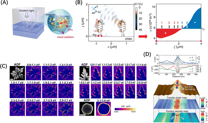 | ||
| Fig. 10 (A) Schematic diagram of photolysis of water by 3D Ag skeleton structure. (B) The simulated electrostatic force distribution in the 3D Ag skeleton and the electron density (n) distribution of the curved plate between the square and triangle symbols. (A and B) Reproduced from ref. 163 with permission from American Chemical Society, copyright 2016. (C) Annular dark field images of fractals (scale = 500 nm), branches (scale = 200 nm), and spherical particles (scale = 500 nm) with EELS intensity maps of their monomers. Reproduced from ref. 164 with permission from American Chemical Society, copyright 2021. (D) Line trace of WSe2 structure (top) and hyperspectral tip-enhanced photoluminescence spectrum and maps of expected tensile strain and exciton density near the fold (bottom). Reproduced from ref. 165 with permission from John Wiley and Sons, copyright 2021. | ||
This “tip effect” of field intensity distribution is also reflected in semiconductor materials. Koo et al. used hyperspectral adaptive tip enhanced PL spectroscopy to show the exciton distribution behaviour in different regions near naturally formed wrinkles in WSe2 monolayers and found that exciton funnel effect occurs at the apex of the fold, and the exciton density is the largest, which is a strong evidence for the formation of local polarization field (Fig. 10D).165 In the case of the specialized material C3N4, research has demonstrated that its light absorption capabilities can be enhanced through the distortion of the planar structure and symmetry of the carbon nitride layer.166 On this basis, Wang et al.167 transformed the geometric form of polyheptahedral imine (PHI) from hexagonal prisms to hexagonal nanosheets by improving the molten salt process, revealing the exact enhancement mechanism behind the performance improvement brought about by morphology modification, namely, the extension of carrier lifetime caused by the regulation of the field range between conjugated layers. Furthermore, Zou et al.168 successfully synthesized ultrathin twisted PHI nanoplates derived from PHI nanosheets. The optimized structural configuration significantly facilitated the n–π* electron transition, achieving an impressive apparent quantum efficiency of 17.3% for photocatalytic hydrogen production from water at a wavelength of 500 nm. These evidences underscore the importance of the deep-level field regulation mechanism in the absorption enhancement attributed to morphological modifications.
4.2 Enhancement of carrier dynamics
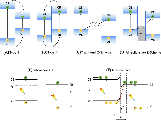 | ||
| Fig. 11 Charge-transfer route in (A) type I, (B) type II, (C) traditional Z-scheme, and (D) all-solid-state Z-scheme heterojunctions. Adapted from ref. 170 with permission from John Wiley and Sons, copyright 2017. Schematic diagram of energy band changes of semiconductors forming S-type heterojunctions before (E) and after (F) contact. Adapted from ref. 171 with permission from Elsevier, copyright 2020. | ||
| Material | Type | Co-catalyst | Reactant | Light source | Gas evolution rate (mol h−1 g−1) | Efficiency | Ref. | |
|---|---|---|---|---|---|---|---|---|
| H2 | O2 | |||||||
| PCOS/Ni2P PCOS: polymeric carbon–oxygen semiconductor | I | NiS | Water containing MnO2 | 300 W Xe lamp λ > 420 nm | 150.7 | 70.2 | AQE = 70% at 420 nm, STH = 0.91% | 176 |
| P25/g-C3N4 | II | Pt | Water | 300 W Xe lamp | 374.2 | 166 | AQE = 0.71% at 400 nm | 177 |
| CdS/Ti3+–SrTiO3 | II | MnOx | Water | 300 W Xe lamp | 176.07 | 86.03 | AQE = 1.21% at 380 nm | 138 |
| Co3(PO4)2/g-C3N4 | II | None | Water | 300 W Xe lamp λ > 400 nm | 375.6 | 177.4 | AQE = 1.32% at 420 nm | 178 |
| ZnO/ZnS | II | Co3O4 | Water | 300 W Xe lamp 780 nm > λ > 320 nm | 3853 | 1927 | AQE = 3.04% at 350 nm | 179 |
| PbTiO3/BiVO4 | Traditional Z | Rh/CrOx Au/CoOx | Water containing Fe2+/Fe3+ | 300 W Xe lamp λ > 420 nm | 48.04 | 24.19 | STH = 0.053% | 180 |
| BiVO4/ZrO2/TaON | Traditional Z | Rh/Cr | Water containing K4 [Fe(CN)6] | 300 W Xe lamp λ ≥ 420 nm | ∼160 | ∼80 | AQE = 12.3% at 420 nm, STH = 0.6% | 181 |
| g-C3N4/ITO/Co–BiVO4 | All solid Z | Pt | Water | 300 W Xe lamp AM 1.5 G | 95.41 | 40.23 | STH = 0.028% | 182 |
| BiVO4/Au/CdS | All solid Z | None | Water | Xe lamp AM 1.5 G | 281 | 138 | STH = 0.054% | 183 |
| In2Se3/CdTe | S | Pt/CoOx | Water | 300 W Xe lamp λ ≥ 300 nm | 101.15 | 47.38 | STH = 1.31% | 184 |
| ZnIn2S4/WO3 | S | Pt/CoOx | Water | 300 W Xe lamp AM 1.5 G | 169.2 | 82.5 | STH = 1.52% | 185 |
| TiO2/ZnIn2S4 | S | None | Water | 300 W Xe lamp | 214.9 | 81.7 | AQE = 11.6% at 420 nm | 186 |
| InVO4/ZnIn2S4 | S | None | Water | 300 W Xe lamp | 153.3 | 76.9 | AQE = 9.75% at 420 nm | 187 |
A built-in electric field can not only form at the interface by assembling two semiconductor photocatalysts, but also within a single semiconductor by engineering the crystal facet exposure of semiconductor crystal materials.188,189 The most typical example is that the (110) and (111) crystal facets of rutile TiO2 that have been identified as the sites of reduction and oxidation reactions, respectively (Fig. 12A).190,194 Subsequently, BiVO4 decahedral-shaped crystals have been favored by researchers due to its excellent photoanisotropy and suitable energy band structure; the e− and h+ separation and accumulation over different crystal facets of a single BiVO4 crystal was also confirmed by Kelvin probe force microscopy (Fig. 12B).191 Besides, SrTiO3 crystals (Fig. 12C) with a narrower band gap and BiOX single crystals (Fig. 12D) that can control the surface atomic coordination of bismuth halide oxide by adjusting the configuration between the [Bi2O2] unit and the halide atoms have also been developed for crystal face control engineering and to introduce the built-in electric field.192,193 It was discovered that the directional separation of photo-induced carriers on different crystal facets is attributed to the difference in space charge regions caused by the different degrees of energy band bending at the surfaces of different crystal facets,195 manifesting in two aspects, i.e., the difference in width and direction of the space charge region, corresponding to the difference in built-in electric field strength and direction respectively (Fig. 12E and F).
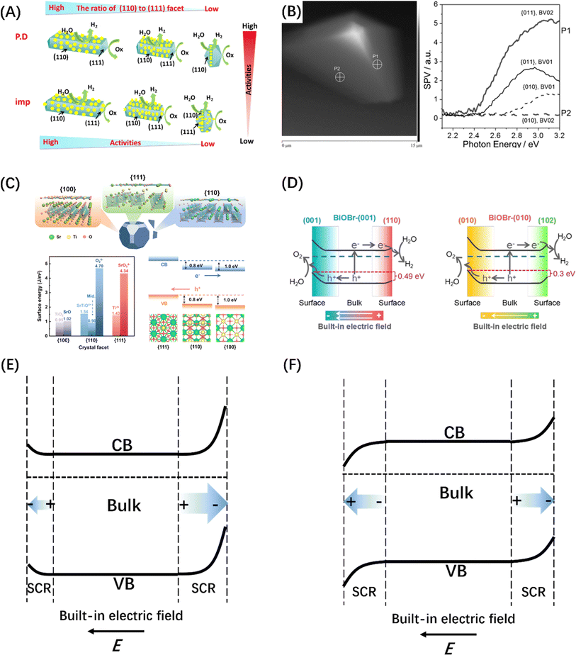 | ||
| Fig. 12 (A) Reduction and oxidation reactions take place on distinct crystal planes of TiO2, specifically on the (110) and (111) planes, respectively. Reproduced from ref. 190 with permission from Elsevier, copyright 2016. (B) The topological representation of a solitary BiVO4 crystal and spatially resolved surface photovoltage spectra obtained from various points. Reproduced from ref. 191 with permission from John Wiley and Sons, copyright 2015. (C) DFT studies of SrTiO3 crystallographic facets. Reproduced from ref. 192 with permission from American Chemical Society, copyright 2024. (D) Illustration depicting the process of charge separation induced by photogeneration in BiOBr-(001) and BiOBr-(010) surfaces, facilitated by the inherent electric field resulting from surface band bending. Reproduced from ref. 193 with permission from John Wiley and Sons, copyright 2020. Schematic diagram of the intensity anisotropy (E) and directional anisotropy (F) built-in electric fields on different crystal facets. | ||
Similarly, the polarization field based on the breakdown of the central symmetry of the crystalline material can also introduce an internal electric field. The direction of the polar surface means that each individual repeating unit grows in a direction perpendicular to the surface, causing the dipole moment of the surface to be non-zero, thus resulting in the generation of electrical and electrostatic power on the polar surface.196 Since the rigidity of some crystals prevents them from using the outer facet to introduce compensating charges to counteract the occurrence of polarity, the presence of macroscopic dipoles can leave considerable polarity and electrostatic force on the polar surface of such crystals.197 The underlying reason for the formation of this electrostatic force may be attributed to the difference in surface band bending caused by different surface polarities, which has been confirmed by the relevant studies on GaN single crystal arrays (Fig. 13A).198 In addition to the polarization field introduced by the selective growth of the polarized surface, surface polarization can also be induced by modifying polar groups, such as hydroxyl groups, on the catalyst surface. For example, the formation of H–O–C![[double bond, length as m-dash]](https://www.rsc.org/images/entities/char_e001.gif) N after the hydroxylation of g-C3N4 surface can foster electron movement to the surface –OH and accelerate the space charge separation, as shown in Fig. 13B.199 The hydroxylation of the surface of BiVO4 (010) can greatly reduce the negative effect of the electron polaron induced by oxygen vacancy and promote the splitting of water (Fig. 13C).200 It is worth mentioning that ferroelectric materials, mainly PbTiO3,202 have an internal electric field induced by spontaneous polarization because of their spontaneous dipole moment, which has also been proven to contribute to the self-separation of photogenerated carriers. Different from the spontaneous polarization of the above materials, confining the catalyst between two polarized crystal facets can also generate a polarization field and achieve the separation effect of photogenerated carriers. Such typical polarized crystal facets include MgO (111), NiO (111), and ZnO (0001).203 For example, the confinement of N-doped TiO2 nanoparticles between the positive and negative terminal surfaces of MgO (111) crystal faces can significantly improve the photogenerated carriers' lifetime (Fig. 13D).201
N after the hydroxylation of g-C3N4 surface can foster electron movement to the surface –OH and accelerate the space charge separation, as shown in Fig. 13B.199 The hydroxylation of the surface of BiVO4 (010) can greatly reduce the negative effect of the electron polaron induced by oxygen vacancy and promote the splitting of water (Fig. 13C).200 It is worth mentioning that ferroelectric materials, mainly PbTiO3,202 have an internal electric field induced by spontaneous polarization because of their spontaneous dipole moment, which has also been proven to contribute to the self-separation of photogenerated carriers. Different from the spontaneous polarization of the above materials, confining the catalyst between two polarized crystal facets can also generate a polarization field and achieve the separation effect of photogenerated carriers. Such typical polarized crystal facets include MgO (111), NiO (111), and ZnO (0001).203 For example, the confinement of N-doped TiO2 nanoparticles between the positive and negative terminal surfaces of MgO (111) crystal faces can significantly improve the photogenerated carriers' lifetime (Fig. 13D).201
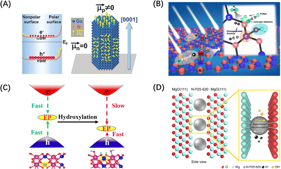 | ||
| Fig. 13 (A) Diagram of different band bending on polar and non-polar surfaces in a GaN crystal. Reproduced from ref. 198 with permission from John Wiley and Sons, copyright 2019. (B) Schematic diagram of charge separation of carbon nitride with surface grafted polymerized hydroxyl group. Reproduced from ref. 199 with permission from Elsevier, copyright 2018. (C) Schematic diagram of hydroxylation alleviating the harmful effects of electron polarons (EP) induced by oxygen vacancies in BiVO4. Reproduced from ref. 200 with permission from American Chemical Society, copyright 2023. (D) Schematic diagram of a polar MgO (111) nanocrystal with two electrical properties applying local electric field restriction to TiO2 nanoparticles. Reproduced from ref. 201 with permission from Springer Nature, copyright 2019. | ||
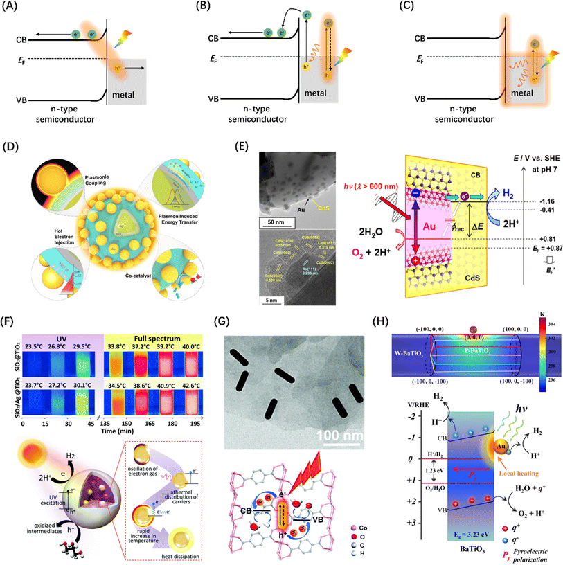 | ||
| Fig. 14 Metal-to-semiconductor charge–separation pathways: (A) plasma-induced direct charge transition at metal–semiconductor interface, (B) the light-excited plasma in the metal decays into hot electron–hole pairs by Landau damping, and (C) thermal effects of plasma decay through ohmic damping. (D) The role of plasma metals in different parts of core-shell-satellite photocatalysts in catalytic reactions. Reproduced from ref. 206 with permission from American Chemical Society, copyright 2021. (E) TEM and HR-TEM images of Au@CdS/ZnO composite structures and LSPR-induced hot electron transfer mechanism. Reproduced from ref. 207 with permission from American Chemical Society, copyright 2018. (F) Infrared images of containers dispersed with SiO2@TiO2 and SiO2/Ag@TiO2 nanocomposites taken under different light sources over time and the corresponding photothermal catalytic mechanism diagram. Reproduced from ref. 208 with permission from Royal Society of Chemistry, copyright 2016. (G) TEM characterization of AuNR/Co-MOFs composites and schematic illustration of HER and OER promotion mechanisms at AuNR/Co-MOFs composites upon light irradiations. Reproduced from ref. 209 with permission from Royal Society of Chemistry, copyright 2020. (H) Temperature distribution of a structural model of Au NP anchored to a BaTiO3 cylinder and schematic diagram of water splitting driven by local heating of a surface plasma. Reproduced from ref. 210 with permission from Springer Nature, copyright 2022. | ||
A study proposed a half-cut Au@CdS core–shell structure, whose external quantum yield can reach 0.24% under 640 nm red light irradiations, originated from the injection of hot electrons generated by selective excitation in the Au core and their separation into the CdS conduction band, as shown in Fig. 14(E).207 Gao et al. designed a SiO2/Ag@TiO2 core–shell structure composite material as a solar thermal collector nanostructure, which has an efficient photothermal performance and can realize the synergistic reaction of seawater catalysis and desalination (Fig. 14F).208 Zhang et al. successfully achieved the simultaneous improvement of HER and OER by anchoring Au nanorods in Co-MOFs materials, and believed that the raising in activity was ascribed to the hot electron injection effect of Au nanorods into Co-MOFs (Fig. 14G).209 Creatively, You et al. introduced a local plasma heat source of Au nanoparticles into the thermocatalytic material BaTiO3, realizing that hot electrons can effectively trigger significantly accelerated multiple thermocatalytic cycle reactions (Fig. 14H).210 Moreover, the SPR effect is closely related to the micromorphology of the metal. So far, various novel morphological metal nanoparticles, such as nanocubes,216 nanorods,217 and nanostars,218 have been developed and used in metal–semiconductor systems for SPR-enhanced photothermal catalytic reactions.
4.3 Charge output promotion
Although the introduction of internal field can boost the dissociation and transport of photogenerated carriers within the catalyst, the photocatalytic reaction activity is largely affected by the surface reaction efficiency of the carriers. This surface reactivity is known to be mainly determined by the high-flux carrier accumulation sites and the catalytic reaction active sites, and when the two are spatially unified, the catalytic reaction efficiency will be doubled.36,219 Co-catalysts are usually modified on the catalyst surface to unify the two sites for POWS reactions. However, it is difficult for a catalyst to be modified with either a HER or OER co-catalysts to achieve overall water splitting, because the POWS process includes both reduction and oxidation processes, and which will affect each other if the high-flux sites and reactive sites are coupled, resulting in ineffective reactions. Therefore, the loading of dual co-catalysts is considered to be an effective modification scheme to achieve POWS.220 Many studies related to TiO2,221 C3N4,222,223 and CdS224 have confirmed that the dual co-catalyst scheme can not only accumulate two types of carriers in the corresponding reaction active sites but also separate the HER and OER reactions on the surface (Fig. 15A–C). Apart from the commonly used HER and OER co-catalysts, the introduction of vacancy defects and ion doping can also achieve the synergistic promotion of the two half reactions on the surface to achieve the effect of complete water splitting. For example, Pan et al. obtained a single-layer ZnIn2S4 nanosheet with double defects (Ag doping and nanopores) through cation exchange, which showed a stoichiometric H2 and O2 release in pure water under visible light irradiations (Fig. 15D).225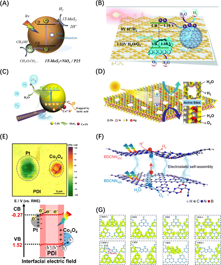 | ||
| Fig. 15 (A) Schematic diagram of carrier space separation in TiO2 enhanced by double co-catalyst MoS2 and NiOx. Reproduced from ref. 221 with permission from Elsevier, copyright 2020. (B) Schematic diagram of the mechanism of electron transfer and POWS in g-C3N4 promoted by double co-catalysts Mn2Co2C@C and MnOOH. Reproduced from ref. 223 with permission from Royal Society of Chemistry, copyright 2020. (C) HER photocatalytic mechanism diagram of MoS2 composites co-modified by CdS and Co-Pi. Reproduced from ref. 224 with permission from American Chemical Society, copyright 2019. (D) Schematic diagram of electrostatic field caused by the introduction of Ag doping and nanoporous defects on ZnIn2S4 monolayer. Reproduced from ref. 225 with permission from American Chemical Society, copyright 2021. (E) A mapping image of the contact potential difference between the double co-catalyst particles and the PDI film in the PDI/Co3O4/Pt heterostructure measured by Kelvin probe and a schematic diagram of the interface charge transfer path. Reproduced from ref. 226 with permission from American Chemical Society, copyright 2023. (F) Charge transfer diagram between g-C3N4 nanosheets with both B-doped and N-vacancy defects. Reproduced from ref. 227 with permission from Springer Nature, copyright 2021. (G) Calculated charge density distribution differences between CB and VB in PCN (top) and Nv–CN (bottom). Reproduced from ref. 228 with permission from Royal Society of Chemistry, copyright 2022. | ||
Briefly, the underlying logic of the dual promoter/defect modification to enhance the performance of POWS is still based on the enhancement mechanism of the built-in electrostatic field/polarization field, but there are different types of multi-directional energy field combinations in the same catalyst, such as heterojunction–heterojunction (electrostatic field-electrostatic field), heterojunction-defect/doping (electrostatic field-polarization field), or defect/doping-defect/doping (polarization field-polarization field), compared with a single heterostructure or doped/defect semiconductor. For example, Li et al. combined the dual co-catalysts Co3O4 and Pt with perylene diimide (PDI) polymer. The dual interfacial electric field constructed by the dual co-catalysts provided an anisotropic driving force for the photogenerated h+ and e− in PDI, synergistically improving the spatial charge separation efficiency of water oxidation (Fig. 15E).226 Zhao et al. designed a Z-type system for photocatalytic water splitting based on boron-doped and nitrogen-defective carbon nitride 2D nanosheets, in which the doping of N and B not only promoted the carrier separation within the monolayer C3N4 plane, but also gave C3N4 different band structures, so that the interlayer electrostatic field was formed between the C3N4 nanosheets doped with the two different elements, as shown in Fig. 15(F).227 Zhang et al. introduced –C![[triple bond, length as m-dash]](https://www.rsc.org/images/entities/char_e002.gif) N groups and N vacancies into g-C3N4 (Nv–C N–CN) in sequence to cause the coexistence of double defects within the plane. Combined with the first-principle calculation results of the charge density distribution in the band structures of the original g-C3N4 and Nv–C N–CN, they proved that the charge density distribution corresponding to Nv–C N–CN is relatively separated when compared with the original g-C3N4, indicating that the modification of the double defect sites can lead to a more localized spatial distribution of the charge density (Fig. 15G), resulting in the improvement of the carrier separation ability.228
N groups and N vacancies into g-C3N4 (Nv–C N–CN) in sequence to cause the coexistence of double defects within the plane. Combined with the first-principle calculation results of the charge density distribution in the band structures of the original g-C3N4 and Nv–C N–CN, they proved that the charge density distribution corresponding to Nv–C N–CN is relatively separated when compared with the original g-C3N4, indicating that the modification of the double defect sites can lead to a more localized spatial distribution of the charge density (Fig. 15G), resulting in the improvement of the carrier separation ability.228
Nevertheless, it should be noted that the reactions occurring on the catalyst surface are very complex, specifically manifested as secondary reactions or cross-reactions of the products, which correspond to ORR reactions and reverse reactions in the POWS process.49 In order to avoid the occurrence of these two types of reactions, there are studies on extra modification of the catalyst surface, i.e., surface coating engineering, finding that the photodeposited oxyhydroxide layer can act as a molecular sieve to selectively filter reactants and products.229 By utilizing the selectivity of the coating, the redox reaction on the photocatalyst surface can be appropriately controlled, leading to successful overall water splitting. However, the thickness and uniformity of the coating are difficult to control.
5. Macroscopic carriers and reaction kinetics
5.1 External energy field assistance
The geometric morphology control of photocatalysts, establishment of built-in fields, and surface modification all involve complex chemical synthesis processes, which limit the application of POWS technology. Especially in relation to the evaluation of POWS reaction efficiency, according to the solar hydrogen production (STH) efficiency standard:230 | (5) |
Additionally, according to the POWS total conversion efficiency (ηtotal) formula:45
| ηtotal = ηabsorption × ηseparation × ηreaction | (6) |
The ηtotal is determined by three parts, namely, photon absorption efficiency (ηabsorption), carrier separation efficiency (ηseparation) and apparent reaction efficiency (ηreaction). The first two can be adjusted by internal field modification, while the latter is mainly determined by the macroscopic reaction rate.
Utilizing external fields in photocatalytic reaction systems is a versatile and manageable approach to boost the apparent photocatalytic activity while keeping the properties of semiconductors unchanged. It has been reported that external field assistance, e.g., external electric fields, thermal fields, and magnetic fields, can significantly improve the macroscopic reaction kinetics on photocatalysts, thereby improving the STH and ηreaction.231
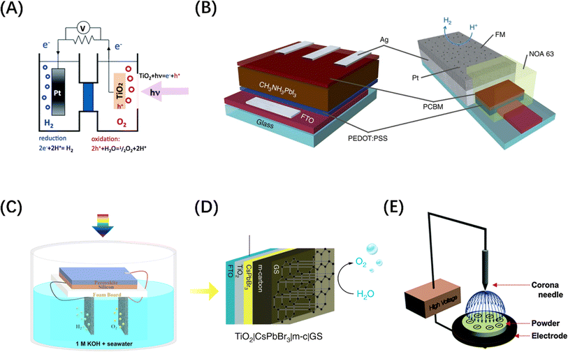 | ||
| Fig. 16 (A) Simple schematic of a photoelectrochemical cell. Reproduced from ref. 232 with permission from Royal Society of Chemistry, copyright 2014. (B) Diagram of a solar cell used as a photocathode for photocatalysis of HER. Reproduced from ref. 79 with permission from Springer Nature, copyright 2016. (C) Schematic diagram of the solar-driven seawater splitting device. Reproduced from ref. 233 with permission from American Chemical Society, copyright 2023. (D) Schematic of CsPbBr3-based multilayer photoanode for photoelectrochemical O2 evolution. Reproduced from ref. 234 with permission from Springer Nature, copyright 2019. (E) Illustration of the corona-poling system. Reproduced from ref. 235 with permission from Royal Society of Chemistry, copyright 2014. | ||
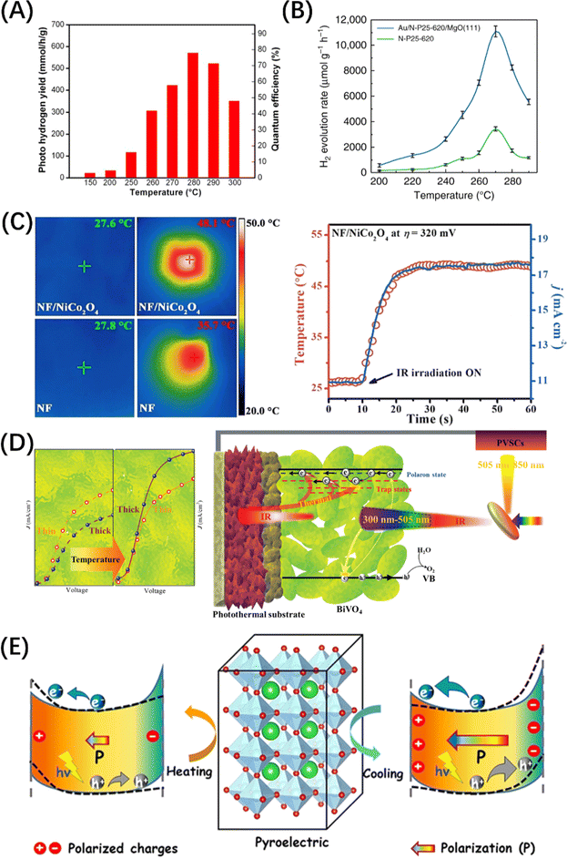 | ||
| Fig. 17 (A) Dependence of photocatalytic HER yield and apparent quantum efficiency on reaction temperature over Pt/black TiO2 catalyst. Reproduced from ref. 242 with permission from American Chemical Society, copyright 2015. (B) Temperature dependence of photocatalytic activity of N-doped P25 and Au/N-doped P25 confined by MgO (111). Reproduced from ref. 201 with permission from Springer Nature, copyright 2019. (C) Thermal images of NF/NiCo2O4 and NF in electrolyte solution under IR radiation and dark conditions and the dependence of temperature and current density j changes on IR radiation time. Reproduced from ref. 243 with permission from Elsevier, copyright 2023. (D) Schematic diagram of photocurrent difference of BiVO4 film with different thickness under light irradiations and schematic diagram of photothermally assisted water splitting. Reproduced from ref. 244 with permission from John Wiley and Sons, copyright 2022. (E) Schematic diagram of carrier separation behaviour and surface band bending differences in pyroelectrics debuted by the pyro-phototropic effect. Reproduced from ref. 231 with permission from John Wiley and Sons, copyright 2021. | ||
Considering that infrared rays contribute nearly half of the solar spectrum, the required heat can be provided by infrared radiation, meaning that high-temperature-promoted photocatalysis can become a new scheme when the heat is provided by solar energy. A study of NiCo2O4 nanoneedles supported by nickel foam (NF) showed that the NF/NiCo2O4 class neural network structure acts as both an infrared absorbing antenna and an OER active anode and confirmed that the enhancement of OER activity is due to the local temperature increase under infrared radiations (Fig. 17C).243 Specifically, infrared radiation reduces the kinetic energy barrier of OER through the infrared thermal effect, thus promoting the OER dynamics. In addition to reducing the reaction thermal barrier, the thermal effect caused by infrared radiations can also stimulate the release of polarons in some interband defect levels and accelerate polaron energy level jumps (Fig. 17D).244 Besides, for a special kind of material, pyroelectric material, the introduction of temperature gradient can not only promote the surface reaction thermodynamically but also induce the generation of polarization field inside the material.231 The temperature-induced creation of positive and negative polarization charges at the extremities of the pyroelectric crystal can enhance charge separation efficiency and control photogenerated carrier transport at the interface, as shown in Fig. 17(E). The resulting thermoelectric potential can modify the surface charge energy, consequently initiating catalytic reactions through thermal catalysis and working in conjunction with the photocatalytic process to facilitate efficient photothermal catalytic reactions.
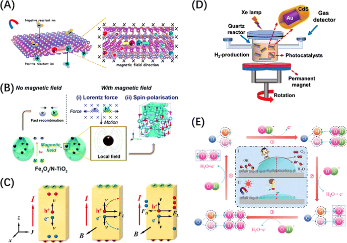 | ||
| Fig. 18 (A) Schematic diagram of macroscopic global charge separation assisted by external magnetic field. Reproduced from ref. 231 with permission from John Wiley and Sons, copyright 2021. (B) Schematic diagram of POWS performance of Au/Fe3O4/N–TiO2 composite material assisted by external magnetic field. Reproduced from ref. 246 with permission from Royal Society of Chemistry, copyright 2022. (C) Schematic diagram of the overall macroscopic charge separation caused by the change of the internal electric field in a polar photocatalyst under the action of the Lorentz force. Reproduced from ref. 23 with permission from American Chemical Society, copyright 2021. (D) Schematic diagram of an experimental setup showing the magnetic field-assisted photocatalytic water splitting system. Reproduced from ref. 247 with permission from Elsevier, copyright 2020. (E) Mechanism diagram of the combination of light and magnetic field to promote OER. Reproduced from ref. 248 with permission from John Wiley and Sons, copyright 2023. | ||
Although the field intensification technology has been developed to a great extent, the role of a single field is limited. It has been reported that the OER activity of Co3O4/CoFe2O4@NF composite photoelectrode materials with both optical and magnetic responsiveness can be improved by synergistically reducing the resistance and increasing the conductivity of the materials under the combined driving forces of optical and magnetic fields, as shown in Fig. 18(E).248 Besides, the electron polarization of the ferromagnetic catalyst under the magnetic field can reduce the potential barrier generated by parallel arranged paramagnetic oxygen and significantly improve the OER reaction kinetics. Therefore, it can be predicted that exploring the mechanism of photocatalysis driven by multi-energy field coupling will be the mainstream trend of future development, which can not only deepen the understanding of external field participation in photocatalytic reactions, but also make up for the possible limitation of a single external field.
5.2 Reaction type design and kinetics for scaling
In addition to modifying the properties of photocatalysts and using an auxiliary external field, it is also necessary to design and innovate the whole photocatalytic reaction to make the technology suitable for practical application. This is of great significance in improving the reaction efficiency and large-scale production research. The type of semiconductor POWS reaction has been developed from the initial electrode reaction to a variety of characteristic and practical systems, among which more common reactions are batch reaction, flow reaction, and gas–solid reaction.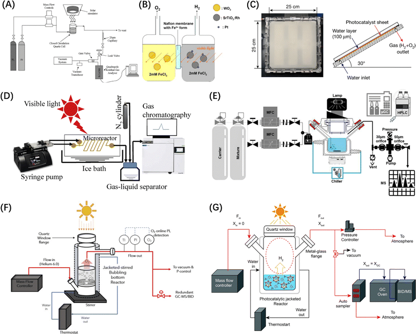 | ||
| Fig. 19 (A) Scheme of a batch water splitting reaction setup. Reproduced from ref. 250 with permission from John Wiley and Sons, copyright 2010. (B) Schematic diagram of a twin-reactor system. Reproduced from ref. 251 with permission from Elsevier, copyright 2010. (C) Photo image of the panel reactor unit and structural diagram of the panel reactor unit seen from the side. Reproduced from ref. 252 with permission from Springer Nature, copyright 2021. (D) Schematic diagram of an optofluidic microreactor for the photocatalytic water splitting. Reproduced from ref. 253 with permission from Elsevier, copyright 2022. (E) Diagram of a multimodal photocatalytic flow system. Reproduced from ref. 254 with permission from AIP Publishing, copyright 2023. (F) Schematic diagram of the evaluation system used to directly quantify the photocatalytic OER rate online. Reproduced from ref. 255 with permission from Elsevier, copyright 2020. (G) Illustration depicting the configuration of a continuous-flow photocatalytic reactor system. Reproduced from ref. 256 with permission from American Chemical Society, copyright 2019. | ||
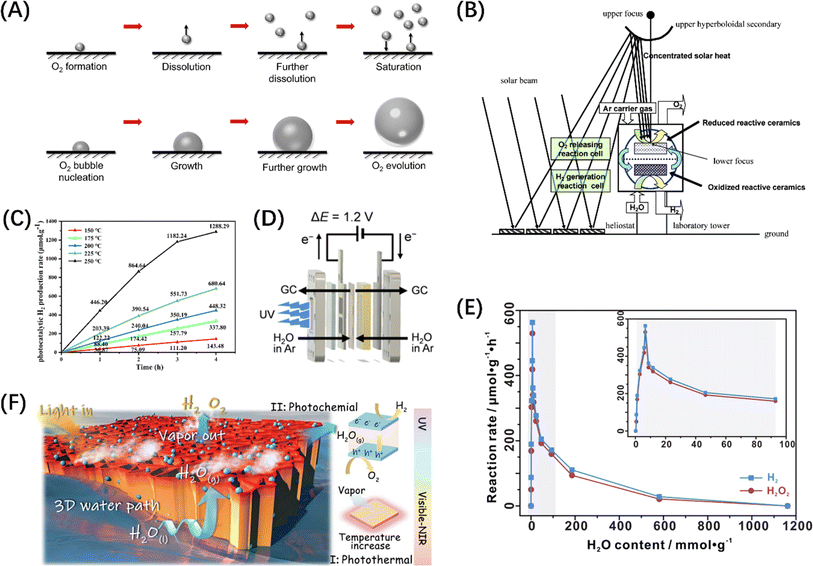 | ||
| Fig. 20 (A) Oxygen evolution diagram in POWS. Reproduced from ref. 49 with permission from Elsevier, copyright 2022. (B) A conceptual outline of a rotary solar reactor. Reproduced from ref. 258 with permission from American Chemical Society, copyright 2007. (C) Photocatalytic H2 production rate at different reaction temperatures over ZnTi. Reproduced from ref. 259 with permission from Royal Society of Chemistry, copyright 2022. (D) Schematic diagram of a gas–solid phase POWS battery. Reproduced from ref. 260 with permission from John Wiley and Sons, copyright 2018. (E) The progression of the observable photocatalytic efficacy in the complete splitting of pure water into H2 and H2O2 in relation to the water concentration on Pt/TiO2. Reproduced from ref. 261 with permission from Elsevier, copyright 2020. (F) Schematic diagram of photothermal catalytic water vapor splitting on TiN silicon wool loaded with K–SrTiO3. Reproduced from ref. 262 with permission from John Wiley and Sons, copyright 2023. | ||
It is premature to assess the advantages and disadvantages of the three aforementioned reactor types solely from the standpoint of the production energy of the reactants, as not all catalysts are suitable for gas–solid reactions. Given the similarity in the energy field mechanisms across these reaction types, it is of practical importance to analyse the methods for enhancing efficiency from the perspective of the energy field. In macroscopic reactions, regardless of the type, the primary objective is to improve the light collection capability of the entire reaction system, which is fundamental to determining the efficiency of large-scale reaction systems.4 Research indicates that nearly half of the incident light is lost prior to being absorbed by the photocatalyst.264 Consequently, optimizing the parameters of the photon field—specifically, the intensity of light absorption and the distribution of photon flux—emerges as a critical factor in enhancing apparent reaction efficiency.
For typical liquid-phase intermittent reactions, which can generally be classified as suspension reactions, sunlight absorption is contingent upon the concentration of particles and the penetration depth of light.4 Therefore, identifying the optimal concentration of the reactive substance and increasing the light penetration depth are two significant strategies for improving macroscopic reaction efficiency. The former can be achieved through the parallel controlled experiments, while the latter can be realized through the optimization of reactor design. For instance, Goto et al. proposed a rectangular panel design for generating hydrogen and oxygen via a POWS reaction.265 This panel reactor features a water layer that is only 1 mm deep, facilitating the rapid release of product bubbles without the need for forced convection, while maximizing the inherent water splitting activity of the particle photocatalyst.
In contrast to batch reactions, the optimization of the photon field in liquid-phase flow reactions must also account for the effects of fluid dynamics.266 For example, Cao et al. introduced a gas disturbance reactor based on fluid dynamics principles. This photoreactor primarily operates under natural circulation, with high-pressure gas intermittently disturbing the deposited photocatalyst.267 By estimating parameters such as radiation distribution and critical flow rate, along with actual reactor commissioning, the necessity of gas perturbation was validated, resulting in optimal average hydrogen production rates of 2.9 L h−1 and 4.0 L h−1 during typical weeks in spring and summer, respectively. Furthermore, the nanofluid reactor presents a more compelling case. For instance, Zhang et al. demonstrated that the incorporation of BaTiO3 nanofluid into the POWS reaction significantly enhanced the hydrogen release rate, achieving a value of 270 mmol h−1 g−1.268 This improvement was attributed to the increased effective area for light irradiation and enhanced particle dispersion. It is evident that the gas–solid phase reaction system can mitigate the effects of suspended particle concentration and light penetration depth on the photon energy field to a certain extent; however, this does not necessarily imply the superiority, particularly in the context of the gas–solid POWS reaction.
The requirement for the temperature to exceed the boiling point of water imposes stringent demands on the temperature field distribution throughout the reaction. Concurrently, the optimization of the photon field must also be addressed, presenting significant challenges in reactor design. Due to the complexities associated with the temperature field control, current gas–solid reaction systems predominantly utilize fixed bed reactors, wherein the catalyst is immobilized within the reactor, such as thin-slit reactors, to maintain a uniform temperature distribution.269 In these systems, planar light is directed onto the catalyst surface via the optical fibre or waveguide technology.270,271 Consequently, it is essential to achieve effective coupling among the reactor, reaction medium, and photocatalyst particles across multiple physical fields to optimize light collection.
6. Conclusions, challenges and future perspectives
This paper reviews strategies to address the contemporary challenges in the POWS physicochemical process, focusing on microscopic and macroscopic modification methods for enhanced photogenerated charge carrier separation and promotion from the perspective of internal/external energy fields. Firstly, in view of the thermodynamic limitations of POWS, we examined the advantages and disadvantages of host semiconductor catalysts such as metal oxides, metal nitrides, metal sulphides, metal halide perovskites, carbon nitrides, and MOFs/COFs, as well as co-catalysts in POWS from the perspective of energy band modulation, combining the water splitting redox potential and the semiconductor band gap structure. Secondly, the mainstream semiconductor modification strategies contained in traditional modification concepts, for example, light absorption enhancement, carrier dynamics enhancement, and charge output promotion, including doping/vacancy engineering, heterojunction construction, crystal plane engineering, polarization engineering, hot electron decay and injection, and surface modification, are thoroughly analysed, and the underlying logic behind them, namely electrostatic field or polarization field, is thoroughly discussed. The role of an external field, such as external electric field, external thermal field, and external magnetic field, and different catalytic reaction systems, including batch reaction, flow reaction, and gas–solid phase reaction, are compared to discuss their improvement effects on macroscopic carriers and reaction kinetics. Finally, the strategies for enhancing the efficiency across various reaction types are critically reviewed from the viewpoint of the photon field. The field enhancement mechanisms corresponding to the modification strategies discussed in this paper are summarized in Fig. 21. Although there are numerous behavioural modifications of photogenerated excitons in POWS physical and chemical processes, there are still many challenges in this field at the overall level, such as the long-term time-consuming and uncertainty of experimental execution, the economic issues of catalytic materials, the instability and discontinuity of natural illumination, and the inefficiency of large-scale catalytic systems. Thus, based on the current efforts, we proposed the prospects for these four major challenges.6.1 Utilization of machine learning vs. the long time and uncertainty of experimental execution
The development of POWS technology has been a topic of research for decades. Both the theoretical basis and practical application have been innovated, however the substantial improvement in efficiency only exists in the laboratory stage, and the economic benefits produced are still far from competing with traditional fossil energy technology. The economic and time costs associated with the development of high-performance materials and the interpretation of microscopic reaction mechanisms have greatly limited development through ‘trial and error’ based investigations. The integration of theoretical principles with practical experimentation is noteworthy for its ability to tackle the complexities associated with the advancement and enhancement of materials used in photocatalytic reactions. This approach serves as a foundational framework for devising innovative strategies to overcome technical obstacles. For example, DFT methods can been used to explore electronic problems, molecular dynamics simulations can describe interactions between large numbers of molecules and surfaces, Monte Carlo simulations can be used for even larger scale explorations, and continuum modelling methods are suitable for length scales close to experimental catalytic systems. Each approach makes a significant contribution to understanding the catalytic behaviour of materials. However, the actual POWS process is multi-length scale. Therefore, for the modelling of complex nanocatalysts, it is foreseeable that the future trend mainly involves combining methods, for instance, using machine learning, over different scales.6.2 Development of new materials vs. economic issues of catalysts
In terms of material economic costs, there are also challenges. For example, precious metals and their oxides are considered to be the most active HER and OER catalysts, respectively, but their large-scale application is severely limited due to their scarcity and high cost. Although the material systems used for POWS have also been greatly expanded, including transition metal oxides, sulphides, nitride, perovskite materials, etc., the development of cost-effective, earth-abundant, and high-performance catalysts remains a difficult task.6.3 Introduction of energy storage systems vs. the instability and intermittency of natural sunlight
The intermittent nature of solar radiation is another objective challenge of POWS technology. Since solar radiation is only available during the day and sunshine also varies with cloud cover and seasons. As a result, the energy supply of a water-splitting reactor is subject to fluctuations of different periods and magnitudes. The resulting unstable operation results in low equipment utilization and reduced competitiveness with fossil fuels and nuclear energy. In order to achieve 24/7 continuous operation, current efforts are mainly focused on the efficient collection of full spectrum sunlight and the configuration of energy storage facilities combined with photothermal effects to maximize the use of photons to generate heat energy and extend the catalytic period after illumination.6.4 Invention of new reactors vs. the inefficiency of large-scale catalytic systems
Promoting the large-scale use of POWS technology is the key to achieving its commercialization, thus it is necessary to develop safe and energy-efficient assembly reactors, which means developing simpler reactors made of lightweight and inexpensive materials but still ensuring safety and durability. At present, most of the research on large-scale POWS applications favours array panel reactors or composite parabolic condensers. To guarantee the consistent and dependable operation of extensive photothermal catalytic reactions, it is imperative to implement precise process control measures. This necessitates the integration of sophisticated monitoring and control systems that can effectively monitor crucial process variables and promptly modify operational settings as required.Data availability
No primary research results, software or code have been included and no new data were generated or analysed as part of this review.Author contributions
Wenhao Zhao: conceptualization, methodology, writing – original draft. Haijun Chen: resources, supervision. Jinqiang Zhang: methodology, writing – review & editing. Paul J. Low: supervision, writing – review & editing. Hongqi Sun: supervision, project administration, writing – review & editing.Conflicts of interest
There are no conflicts to declare.Acknowledgements
The authors would like to acknowledge the financial support from the Australian Research Council Discovery Project (DP240102787) and Future Fellowship (FT240100475).References
- H. Ahmad, S. K. Kamarudin, L. J. Minggu and M. Kassim, Renewable Sustainable Energy Rev., 2015, 43, 599–610 CrossRef CAS.
- A. Fujishima and K. Honda, Nature, 1972, 238, 37–38 CrossRef CAS PubMed.
- C. S. Gopinath and N. Nalajala, J. Mater. Chem. A, 2021, 9, 1353–1371 RSC.
- L. Guo, Y. Chen, J. Su, M. Liu and Y. Liu, Energy, 2019, 172, 1079–1086 CrossRef CAS.
- T. Hisatomi and K. Domen, Nat. Catal., 2019, 2, 387–399 CrossRef CAS.
- P. Zhou, I. A. Navid, Y. Ma, Y. Xiao, P. Wang, Z. Ye, B. Zhou, K. Sun and Z. Mi, Nature, 2023, 613, 66–70 CrossRef CAS PubMed.
- S. K. Lakhera, A. Rajan, T. P. Rugma and N. Bernaurdshaw, Renewable Sustainable Energy Rev., 2021, 152, 111694 CrossRef CAS.
- N. Fajrina and M. Tahir, Int. J. Hydrogen Energy, 2019, 44, 540–577 CrossRef CAS.
- K. Maeda, J. Photochem. Photobiol., C, 2011, 12, 237–268 CrossRef CAS.
- K. Maeda, D. Lu, K. Teramura and K. Domen, Energy Environ. Sci., 2010, 3, 470–477 RSC.
- K. Maeda, R. Abe and K. Domen, J. Phys. Chem. C, 2011, 115, 3057–3064 CrossRef CAS.
- W. J. Youngblood, S.-H. A. Lee, Y. Kobayashi, E. A. Hernandez-Pagan, P. G. Hoertz, T. A. Moore, A. L. Moore, D. Gust and T. E. Mallouk, J. Am. Chem. Soc., 2009, 131, 926–927 CrossRef CAS PubMed.
- K. Maeda, K. Teramura, D. Lu, N. Saito, Y. Inoue and K. Domen, Angew. Chem., Int. Ed., 2006, 45, 7806–7809 CrossRef CAS PubMed.
- J. S. Jang, H. G. Kim and J. S. Lee, Catal. Today, 2012, 185, 270–277 CrossRef CAS.
- S. J. A. Moniz, S. A. Shevlin, D. J. Martin, Z.-X. Guo and J. Tang, Energy Environ. Sci., 2015, 8, 731–759 RSC.
- S. Xu, S. Gong, H. Jiang, P. Shi, J. Fan, Q. Xu and Y. Min, Appl. Catal., B, 2020, 267, 118661 CrossRef CAS.
- L. Zhang, J. Zhang, H. Yu and J. Yu, Adv. Mater., 2022, 34, 2107668 CrossRef CAS PubMed.
- Z. Zheng, W. Xie, B. Huang and Y. Dai, Chem.–Eur. J., 2018, 24, 18322–18333 CrossRef CAS PubMed.
- T. Lv, J. Li, N. Arif, L. Qi, J. Lu, Z. Ye and Y.-J. Zeng, Matter, 2022, 5, 2685–2721 CrossRef CAS.
- Y. Li, J. Li, W. Yang and X. Wang, Nanoscale Horiz., 2020, 5, 1174–1187 RSC.
- X. Chen, J. Wang, Y. Chai, Z. Zhang and Y. Zhu, Adv. Mater., 2021, 33, 2007479 CrossRef CAS PubMed.
- D. Ge, R. Luo, X. Wang, L. Yang, W. Xiong and F. Wang, Appl. Surf. Sci., 2021, 566, 150639 CrossRef CAS.
- X. Li, W. Wang, F. Dong, Z. Zhang, L. Han, X. Luo, J. Huang, Z. Feng, Z. Chen, G. Jia and T. Zhang, ACS Catal., 2021, 11, 4739–4769 CrossRef CAS.
- Z. Liu, W. Hou, P. Pavaskar, M. Aykol and S. B. Cronin, Nano Lett., 2011, 11, 1111–1116 CrossRef CAS PubMed.
- L. Chen, J.-T. Ren and Z.-Y. Yuan, Adv. Energy Mater., 2023, 13, 2203720 CrossRef CAS.
- T. Takata, J. Jiang, Y. Sakata, M. Nakabayashi, N. Shibata, V. Nandal, K. Seki, T. Hisatomi and K. Domen, Nature, 2020, 581, 411–414 CrossRef CAS PubMed.
- Y. Li, H. Zhou, S. Cai, D. Prabhakaran, W. Niu, A. Large, G. Held, R. A. Taylor, X.-P. Wu and S. C. E. Tsang, Nat. Catal., 2024, 7, 77–88 CrossRef CAS.
- X. Yue, J. Fan and Q. Xiang, Adv. Funct. Mater., 2022, 32, 2110258 CrossRef CAS.
- J. Li, L. Cai, J. Shang, Y. Yu and L. Zhang, Adv. Mater., 2016, 28, 4059–4064 CrossRef CAS.
- S. Bai, N. Zhang, C. Gao and Y. Xiong, Nano Energy, 2018, 53, 296–336 CrossRef CAS.
- Y. Zhou, Y. Liang, J. Fu, K. Liu, Q. Chen, X. Wang, H. Li, L. Zhu, J. Hu, H. Pan, M. Miyauchi, L. Jiang, E. Cortés and M. Liu, Nano Lett., 2022, 22, 1963–1970 CrossRef CAS PubMed.
- J. Li, J. Pan, W. Yin, Y. Cai, H. Huang, Y. He, G. Gong, Y. Yuan, C. Fan, Q. Zhang and L. Wang, Chin. Chem. Lett., 2023, 34, 108049 CrossRef CAS.
- S. Luo, X. Ren, H. Lin, H. Song and J. Ye, Chem. Sci., 2021, 12, 5701–5719 RSC.
- L. Mascaretti and A. Naldoni, J. Appl. Phys., 2020, 128, 041101 CrossRef CAS.
- H. D. Ha, C. Yan, G. Katsoukis, G. A. Kamat, I. A. Moreno-Hernandez, H. Frei and A. P. Alivisatos, Nano Lett., 2020, 20, 8661–8667 CrossRef CAS PubMed.
- J. Zhang, H. Chen, X. Duan, H. Sun and S. Wang, Mater. Today, 2023, 68, 234–253 CrossRef CAS.
- K. Sun, Y. Qian and H.-L. Jiang, Angew. Chem., Int. Ed., 2023, 62, e202217565 CrossRef CAS PubMed.
- H. Zhao, L. Jian, M. Gong, M. Jing, H. Li, Q. Mao, T. Lu, Y. Guo, R. Ji, W. Chi, Y. Dong and Y. Zhu, Small Struct., 2022, 3, 2100229 CrossRef CAS.
- X. Tao, Y. Zhao, S. Wang, C. Li and R. Li, Chem. Soc. Rev., 2022, 51, 3561–3608 RSC.
- A. L. Linsebigler, G. Lu and J. T. Yates Jr, Chem. Rev., 1995, 95, 735–758 CrossRef CAS.
- J. Tang, J. R. Durrant and D. R. Klug, J. Am. Chem. Soc., 2008, 130, 13885–13891 CrossRef CAS PubMed.
- R. Qian, H. Zong, J. Schneider, G. Zhou, T. Zhao, Y. Li, J. Yang, D. W. Bahnemann and J. H. Pan, Catal. Today, 2019, 335, 78–90 CrossRef CAS.
- U. Ulmer, T. Dingle, P. N. Duchesne, R. H. Morris, A. Tavasoli, T. Wood and G. A. Ozin, Nat. Commun., 2019, 10, 3169 CrossRef PubMed.
- J. Yang, D. Wang, H. Han and C. Li, Acc. Chem. Res., 2013, 46, 1900–1909 CrossRef CAS PubMed.
- Q. Wang and K. Domen, Chem. Rev., 2020, 120, 919–985 CrossRef CAS PubMed.
- S. Chen, T. Takata and K. Domen, Nat. Rev. Mater., 2017, 2, 17050 CrossRef CAS.
- C. Kranz and M. Wächtler, Chem. Soc. Rev., 2021, 50, 1407–1437 RSC.
- J. Zhang, P. Zhou, J. Liu and J. Yu, Phys. Chem. Chem. Phys., 2014, 16, 20382–20386 RSC.
- C. Bie, L. Wang and J. Yu, Chem, 2022, 8, 1567–1574 CAS.
- S. Navalón, A. Dhakshinamoorthy, M. Álvaro, B. Ferrer and H. García, Chem. Rev., 2023, 123, 445–490 CrossRef PubMed.
- Q. Lu, Y. Yu, Q. Ma, B. Chen and H. Zhang, Adv. Mater., 2016, 28, 1917–1933 CrossRef CAS PubMed.
- L. Guo, X. Yao, Z. Wang, C. Luo, L. Zhou, F. Liu, R. Zhang and X. Wang, Small, 2024, 20, 2310753 CrossRef CAS PubMed.
- H. Wu, R. Irani, K. Zhang, L. Jing, H. Dai, H. Y. Chung, F. F. Abdi and Y. H. Ng, ACS Energy Lett., 2021, 6, 3400–3407 CrossRef CAS.
- R. M. Navarro Yerga, M. C. Álvarez Galván, F. del Valle, J. A. Villoria de la Mano and J. L. G. Fierro, ChemSusChem, 2009, 2, 471–485 CrossRef CAS PubMed.
- A. Mills and S. Le Hunte, J. Photochem. Photobiol., A, 1997, 108, 1–35 CrossRef CAS.
- K. Maeda and K. Domen, J. Phys. Chem. C, 2007, 111, 7851–7861 CrossRef CAS.
- Q.-L. Liu, Z.-Y. Zhao and J.-H. Yi, Phys. Chem. Chem. Phys., 2018, 20, 12005–12015 RSC.
- Y. Pihosh, V. Nandal, R. Shoji, R. Bekarevich, T. Higashi, V. Nicolosi, H. Matsuzaki, K. Seki and K. Domen, ACS Energy Lett., 2023, 8, 2106–2112 CrossRef CAS.
- Y. Wang, Y. Wu, K. Sun and Z. Mi, Mater. Horiz., 2019, 6, 1454–1462 RSC.
- P. Zhang, D. Luan and X. W. Lou, Adv. Mater., 2020, 32, 2004561 CrossRef CAS PubMed.
- X. Ning and G. Lu, Nanoscale, 2020, 12, 1213–1223 RSC.
- R. Yang, L. Mei, Y. Fan, Q. Zhang, R. Zhu, R. Amal, Z. Yin and Z. Zeng, Small Methods, 2021, 5, 2100887 CrossRef CAS.
- C. Yuan, X. Zou, F. He, Y. Dong, Y. Cui, H. Ge and Y. Hou, Adv. Energy Sustainability Res., 2022, 3, 2200012 CrossRef CAS.
- X. Wang, T. Shi, X. Wang, A. Song, G. Li, L. Wang, J. Huang, A. Meng and Z. Li, J. Energy Chem., 2024, 92, 151–161 CrossRef CAS.
- X. Xin, Y. Li, Y. Zhang, Y. Wang, X. Chi, Y. Wei, C. Diao, J. Su, R. Wang, P. Guo, J. Yu, J. Zhang, A. J. Sobrido, M.-M. Titirici and X. Li, Nat. Commun., 2024, 15, 337 CrossRef CAS PubMed.
- J. Sato, N. Saito, Y. Yamada, K. Maeda, T. Takata, J. N. Kondo, M. Hara, H. Kobayashi, K. Domen and Y. Inoue, J. Am. Chem. Soc., 2005, 127, 4150–4151 CrossRef CAS PubMed.
- M. G. Kibria, R. Qiao, W. Yang, I. Boukahil, X. Kong, F. A. Chowdhury, M. L. Trudeau, W. Ji, H. Guo, F. J. Himpsel, L. Vayssieres and Z. Mi, Adv. Mater., 2016, 28, 8388–8397 CrossRef CAS PubMed.
- Q. Wang, M. Nakabayashi, T. Hisatomi, S. Sun, S. Akiyama, Z. Wang, Z. Pan, X. Xiao, T. Watanabe, T. Yamada, N. Shibata, T. Takata and K. Domen, Nat. Mater., 2019, 18, 827–832 CrossRef CAS.
- G. Wang, B. Huang, Z. Li, Z. Lou, Z. Wang, Y. Dai and M.-H. Whangbo, Sci. Rep., 2015, 5, 8544 CrossRef CAS PubMed.
- B. Weng, M.-Y. Qi, C. Han, Z.-R. Tang and Y.-J. Xu, ACS Catal., 2019, 9, 4642–4687 CrossRef CAS.
- W.-K. Chong, B.-J. Ng, Y. J. Lee, L.-L. Tan, L. K. Putri, J. Low, A. R. Mohamed and S.-P. Chai, Nat. Commun., 2023, 14, 7676 CrossRef CAS PubMed.
- K. Ren, S. Yue, C. Li, Z. Fang, K. A. M. Gasem, J. Leszczynski, S. Qu, Z. Wang and M. Fan, J. Mater. Chem. A, 2022, 10, 407–429 RSC.
- C. Li, J. Wei, M. Sato, H. Koike, Z.-Z. Xie, Y.-Q. Li, K. Kanai, S. Kera, N. Ueno and J.-X. Tang, ACS Appl. Mater. Interfaces, 2016, 8, 11526–11531 CrossRef CAS.
- K. Ogawa, H. Suzuki, C. Zhong, R. Sakamoto, O. Tomita, A. Saeki, H. Kageyama and R. Abe, J. Am. Chem. Soc., 2021, 143, 8446–8453 CrossRef CAS.
- Y. Wang, Y. Kang, H. Zhu, G. Liu, J. T. S. Irvine and X. Xu, Adv. Sci., 2021, 8, 2003343 CrossRef CAS.
- A. M. K. Fehr, A. Agrawal, F. Mandani, C. L. Conrad, Q. Jiang, S. Y. Park, O. Alley, B. Li, S. Sidhik, I. Metcalf, C. Botello, J. L. Young, J. Even, J. C. Blancon, T. G. Deutsch, K. Zhu, S. Albrecht, F. M. Toma, M. Wong and A. D. Mohite, Nat. Commun., 2023, 14, 3797 CrossRef CAS PubMed.
- N.-G. Park, ACS Energy Lett., 2019, 4, 2983–2985 CrossRef CAS.
- J. Luo, J.-H. Im, M. T. Mayer, M. Schreier, M. K. Nazeeruddin, N.-G. Park, S. D. Tilley, H. J. Fan and M. Grätzel, Science, 2014, 345, 1593–1596 CrossRef CAS PubMed.
- M. Crespo-Quesada, L. M. Pazos-Outón, J. Warnan, M. F. Kuehnel, R. H. Friend and E. Reisner, Nat. Commun., 2016, 7, 12555 CrossRef CAS PubMed.
- M. T. Hoang, N. D. Pham, J. H. Han, J. M. Gardner and I. Oh, ACS Appl. Mater. Interfaces, 2016, 8, 11904–11909 CrossRef CAS PubMed.
- H. Huang, B. Pradhan, J. Hofkens, M. B. J. Roeffaers and J. A. Steele, ACS Energy Lett., 2020, 5, 1107–1123 CrossRef CAS.
- S. Cao, J. Low, J. Yu and M. Jaroniec, Adv. Mater., 2015, 27, 2150–2176 CrossRef CAS PubMed.
- A. Mishra, A. Mehta, S. Basu, N. P. Shetti, K. R. Reddy and T. M. Aminabhavi, Carbon, 2019, 149, 693–721 CrossRef CAS.
- X. Wang, K. Maeda, A. Thomas, K. Takanabe, G. Xin, J. M. Carlsson, K. Domen and M. Antonietti, Nat. Mater., 2009, 8, 76–80 CrossRef CAS PubMed.
- Q. Xiang, J. Yu and M. Jaroniec, J. Phys. Chem. C, 2011, 115, 7355–7363 CrossRef CAS.
- H. Wang, X. Li and J. Yang, ChemPhysChem, 2016, 17, 2100–2104 CrossRef CAS PubMed.
- P. He, D. Deng, T. Ren, Y. Dang, M. Li, J. Chen and Y. Xiao, Eur. J. Inorg. Chem., 2022, 2022, e202200003 CrossRef CAS.
- H. Wang, W. Zhou, P. Li, X. Tan, Y. Liu, W. Hu, J. Ye and T. Yu, J. Phys. Chem. C, 2018, 122, 17261–17267 CrossRef CAS.
- Z. Ai, Y. Shao, B. Chang, L. Zhang, J. Shen, Y. Wu, B. Huang and X. Hao, Appl. Catal., B, 2019, 259, 118077 CrossRef CAS.
- C. Ye, J.-X. Li, Z.-J. Li, X.-B. Li, X.-B. Fan, L.-P. Zhang, B. Chen, C.-H. Tung and L.-Z. Wu, ACS Catal., 2015, 5, 6973–6979 CrossRef CAS.
- D. Sun, X. Zhang, A. Shi, C. Quan, S. Xiao, S. Ji, Z. Zhou, X. a. Li, F. Chi and X. Niu, Appl. Surf. Sci., 2022, 601, 154186 CrossRef CAS.
- I. Y. Kim, S. Kim, S. Premkumar, J.-H. Yang, S. Umapathy and A. Vinu, Small, 2020, 16, 1903572 CrossRef CAS PubMed.
- X. Li, Z. Wang and L. Wang, Small Sci., 2021, 1, 2000074 CrossRef CAS.
- K. Meyer, M. Ranocchiari and J. A. van Bokhoven, Energy Environ. Sci., 2015, 8, 1923–1937 RSC.
- C.-C. Gu, F.-H. Xu, W.-K. Zhu, R.-J. Wu, L. Deng, J. Zou, B.-C. Weng and R.-L. Zhu, Chem. Commun., 2023, 59, 7302–7320 RSC.
- Q. Yang, M. Luo, K. Liu, H. Cao and H. Yan, Appl. Catal., B, 2020, 276, 119174 CrossRef CAS.
- X. Qiu, Y. Zhu, X. Zhang, Y. Zhang, L. T. Menisa, C. Xia, S. Liu and Z. Tang, Sol. RRL, 2020, 4, 1900449 CrossRef CAS.
- Y. Chen, X. Luo, J. Zhang, L. Hu, T. Xu, W. Li, L. Chen, M. Shen, S.-B. Ren, D.-M. Han, G.-H. Ning and D. Li, J. Mater. Chem. A, 2022, 10, 24620–24627 RSC.
- Y. Xiao, Y. Qi, X. Wang, X. Wang, F. Zhang and C. Li, Adv. Mater., 2018, 30, 1803401 CrossRef PubMed.
- S. Zhang, G. Cheng, L. Guo, N. Wang, B. Tan and S. Jin, Angew. Chem., Int. Ed., 2020, 59, 6007–6014 CrossRef CAS PubMed.
- S. E. Gledhill, B. Scott and B. A. Gregg, J. Mater. Res., 2005, 20, 3167–3179 CrossRef CAS.
- M. Rahman, H. Tian and T. Edvinsson, Angew. Chem., Int. Ed., 2020, 59, 16278–16293 CrossRef CAS PubMed.
- V. Arkhipov, P. Heremans and H. Bassler, Appl. Phys. Lett., 2003, 82, 4605–4607 CrossRef CAS.
- J. Ran, J. Zhang, J. Yu, M. Jaroniec and S. Z. Qiao, Chem. Soc. Rev., 2014, 43, 7787–7812 RSC.
- J. Zhu, J. Xiong, G. Cheng, W. Li and S. Dou, J. Colloid Interface Sci., 2019, 545, 116–127 CrossRef CAS PubMed.
- K. C. Christoforidis, Z. Syrgiannis, V. La Parola, T. Montini, C. Petit, E. Stathatos, R. Godin, J. R. Durrant, M. Prato and P. Fornasiero, Nano Energy, 2018, 50, 468–478 CrossRef CAS.
- Z. Zhuang, Y. Li, Z. Li, F. Lv, Z. Lang, K. Zhao, L. Zhou, L. Moskaleva, S. Guo and L. Mai, Angew. Chem., Int. Ed., 2018, 57, 496–500 CrossRef CAS PubMed.
- J. Ran, H. Wang, H. Jin, C. Ling, X. Zhang, H. Ju, L. Jing, J. Wang, R. Zheng and S.-Z. Qiao, J. Mater. Chem. A, 2018, 6, 23278–23282 RSC.
- X.-j. Wang, X. Tian, Y.-j. Sun, J.-y. Zhu, F.-t. Li, H.-y. Mu and J. Zhao, Nanoscale, 2018, 10, 12315–12321 RSC.
- Q. Wang, J. Huang, H. Sun, Y. H. Ng, K.-Q. Zhang and Y. Lai, ChemSusChem, 2018, 11, 1708–1721 CrossRef CAS PubMed.
- N. L. Reddy, S. Emin, V. D. Kumari and S. Muthukonda Venkatakrishnan, Ind. Eng. Chem. Res., 2018, 57, 568–577 CrossRef CAS.
- C. Han, Y. Gao, S. Liu, L. Ge, N. Xiao, D. Dai, B. Xu and C. Chen, Int. J. Hydrogen Energy, 2017, 42, 22765–22775 CrossRef CAS.
- X. Han, D. Xu, L. An, C. Hou, Y. Li, Q. Zhang and H. Wang, Appl. Catal., B, 2019, 243, 136–144 CrossRef CAS.
- X. Yue, S. Yi, R. Wang, Z. Zhang and S. Qiu, Appl. Catal., B, 2018, 224, 17–26 CrossRef CAS.
- Y. Dong, Q. Han, Q. Hu, C. Xu, C. Dong, Y. Peng, Y. Ding and Y. Lan, Appl. Catal., B, 2021, 293, 120214 CrossRef CAS.
- W. Wang, Y. Tao, J. Fan, Z. Yan, H. Shang, D. L. Phillips, M. Chen and G. Li, Adv. Funct. Mater., 2022, 32, 2201357 CrossRef CAS.
- L. Tian, F. Wang, Z. Zhang and S. Min, Int. J. Hydrogen Energy, 2020, 45, 19017–19026 CrossRef CAS.
- Y. Qu, N. Sun, M. Humayun, A. Zada, Y. Xie, J. Tang, L. Jing and H. Fu, Sustainable Energy Fuels, 2018, 2, 549–552 RSC.
- D. Zeng, T. Zhou, W.-J. Ong, M. Wu, X. Duan, W. Xu, Y. Chen, Y.-A. Zhu and D.-L. Peng, ACS Appl. Mater. Interfaces, 2019, 11, 5651–5660 CrossRef CAS PubMed.
- D. Zeng, W. Xu, W.-J. Ong, J. Xu, H. Ren, Y. Chen, H. Zheng and D.-L. Peng, Appl. Catal., B, 2018, 221, 47–55 CrossRef CAS.
- R. Shen, J. Xie, X. Lu, X. Chen and X. Li, ACS Sustain. Chem. Eng., 2018, 6, 4026–4036 CrossRef CAS.
- Y. Pei, Y. Cheng, J. Chen, W. Smith, P. Dong, P. M. Ajayan, M. Ye and J. Shen, J. Mater. Chem. A, 2018, 6, 23220–23243 RSC.
- H. Yang, J. Yin, R. Cao, P. Sun, S. Zhang and X. Xu, Sci. Bull., 2019, 64, 1510–1517 CrossRef CAS PubMed.
- F. Xue, M. Liu, C. Cheng, J. Deng and J. Shi, ChemCatChem, 2018, 10, 5441–5448 CrossRef CAS.
- O. Cavdar, A. Malankowska, D. Amgar, P. Mazierski, J. Łuczak, W. Lisowski and A. Zaleska-Medynska, Int. J. Hydrogen Energy, 2021, 46, 486–498 CrossRef CAS.
- S. Lv, Y. Wang, Y. Zhou, Q. Liu, C. Song and D. Wang, J. Alloys Compd., 2021, 868, 159144 CrossRef CAS.
- X. Chen, B. Sun, J. Chu, Z. Han, Y. Wang, Y. Du, X. Han and P. Xu, ACS Appl. Mater. Interfaces, 2022, 14, 28945–28955 CrossRef CAS PubMed.
- S. Qiu, R. Guo, Q. Wang, F. Yang, Y. Han, X. Peng, H. Yuan and X. Wang, Int. J. Energy Res., 2021, 45, 14985–14994 CrossRef CAS.
- H. She, X. Ma, K. Chen, H. Liu, J. Huang, L. Wang and Q. Wang, J. Alloys Compd., 2020, 821, 153239 CrossRef CAS.
- D. McAteer, I. J. Godwin, Z. Ling, A. Harvey, L. He, C. S. Boland, V. Vega-Mayoral, B. Szydłowska, A. A. Rovetta, C. Backes, J. B. Boland, X. Chen, M. E. G. Lyons and J. N. Coleman, Adv. Energy Mater., 2018, 8, 1702965 CrossRef.
- T. Feng, J. Ding, H. Li, W. Wang, B. Dong and L. Cao, ChemSusChem, 2021, 14, 3382–3390 CrossRef CAS PubMed.
- X. Zhu, Y. Liu, M. Wang, L. Zhang, Q. Li, E. Zhang, H. Mo, Y. Gao, C. Xu and Y. Zhang, Chem. Eng. J., 2024, 479, 147636 CrossRef CAS.
- S. Fang, S. Li, L. Ge, C. Han, P. Qiu and Y. Gao, Dalton Trans., 2017, 46, 10578–10585 RSC.
- W. Liu, L. Cao, W. Cheng, Y. Cao, X. Liu, W. Zhang, X. Mou, L. Jin, X. Zheng, W. Che, Q. Liu, T. Yao and S. Wei, Angew. Chem., Int. Ed., 2017, 56, 9312–9317 CrossRef CAS PubMed.
- C. Chu, Q. Zhu, Z. Pan, S. Gupta, D. Huang, Y. Du, S. Weon, Y. Wu, C. Muhich, E. Stavitski, K. Domen and J.-H. Kim, Proc. Natl. Acad. Sci. U.S.A., 2020, 117, 6376–6382 CrossRef CAS PubMed.
- S. Sun, Y.-C. Zhang, G. Shen, Y. Wang, X. Liu, Z. Duan, L. Pan, X. Zhang and J.-J. Zou, Appl. Catal., B, 2019, 243, 253–261 CrossRef CAS.
- Y. Zhang, L. Shi, Z. Geng, T. Ren and Z. Yang, Sci. Rep., 2019, 9, 19090 CrossRef CAS PubMed.
- J. Pan, Z. Chen, P. Wang, P. Wang, Q. Yu, W. Zhao, J. Wang, M. Zhu, Y. Zheng and C. Li, Chem. Eng. J., 2021, 424, 130357 CrossRef CAS.
- C. Cheng, L. Mao, J. Shi, F. Xue, S. Zong, B. Zheng and L. Guo, J. Mater. Chem. A, 2021, 9, 12299–12306 RSC.
- H. Zhang, W. Tian, X. Duan, H. Sun, S. Liu and S. Wang, Adv. Mater., 2020, 32, 1904037 CrossRef CAS PubMed.
- S. Wang, J. Zhang, B. Li, H. Sun and S. Wang, Energy Fuels, 2021, 35, 6504–6526 CrossRef CAS.
- G. Liu, L. Wang, H. G. Yang, H.-M. Cheng and G. Q. Lu, J. Mater. Chem., 2010, 20, 831–843 RSC.
- X. Ma, X. Cui, Z. Zhao, M. A. Melo, E. J. Roberts and F. E. Osterloh, J. Mater. Chem. A, 2018, 6, 5774–5781 RSC.
- R. Asahi, T. Morikawa, T. Ohwaki, K. Aoki and Y. Taga, Science, 2001, 293, 269–271 CrossRef CAS PubMed.
- B. Xiao, T. Lv, J. Zhao, Q. Rong, H. Zhang, H. Wei, J. He, J. Zhang, Y. Zhang, Y. Peng and Q. Liu, ACS Catal., 2021, 11, 13255–13265 CrossRef CAS.
- B. Sun, J. Bu, X. Chen, D. Fan, S. Li, Z. Li, W. Zhou and Y. Du, Chem. Eng. J., 2022, 435, 135074 CrossRef CAS.
- W.-K. Chong, B.-J. Ng, X. Y. Kong, L.-L. Tan, L. K. Putri and S.-P. Chai, Appl. Catal., B, 2023, 325, 122372 CrossRef CAS.
- G. Wan, L. Yin, X. Chen, X. Xu, J. Huang, C. Zhen, H. Zhu, B. Huang, W. Hu, Z. Ren, H. Tian, L. Wang, G. Liu and H.-M. Cheng, J. Am. Chem. Soc., 2022, 144, 20342–20350 CrossRef CAS PubMed.
- C. Wang, Z. Chen, H. Jin, C. Cao, J. Li and Z. Mi, J. Mater. Chem. A, 2014, 2, 17820–17827 RSC.
- Y. Wang, R. Zhang, J. Li, L. Li and S. Lin, Nanoscale Res. Lett., 2014, 9, 46 CrossRef PubMed.
- M. Nasirian, Y. P. Lin, C. F. Bustillo-Lecompte and M. Mehrvar, Int. J. Environ. Sci. Technol., 2018, 15, 2009–2032 CrossRef CAS.
- X. Zhao, J. Feng, S. Chen, Y. Huang, T. C. Sum and Z. Chen, Phys. Chem. Chem. Phys., 2017, 19, 1074–1082 RSC.
- J. He, L. Hu, C. Shao, S. Jiang, C. Sun and S. Song, ACS Nano, 2021, 15, 18006–18013 CrossRef CAS PubMed.
- C. M. Wolff, P. D. Frischmann, M. Schulze, B. J. Bohn, R. Wein, P. Livadas, M. T. Carlson, F. Jäckel, J. Feldmann, F. Würthner and J. K. Stolarczyk, Nat. Energy, 2018, 3, 862–869 CrossRef CAS.
- B. Zhou, X. Kong, S. Vanka, S. Chu, P. Ghamari, Y. Wang, N. Pant, I. Shih, H. Guo and Z. Mi, Nat. Commun., 2018, 9, 3856 CrossRef PubMed.
- J. Tian, Y. Zhang, L. Du, Y. He, X.-H. Jin, S. Pearce, J.-C. Eloi, R. L. Harniman, D. Alibhai, R. Ye, D. L. Phillips and I. Manners, Nat. Chem., 2020, 12, 1150–1156 CrossRef CAS PubMed.
- X. Lv, X. Li, C. Yang, X. Ding, Y. Zhang, Y.-Z. Zheng, S. Li, X. Sun and X. Tao, Adv. Funct. Mater., 2020, 30, 1910830 CrossRef CAS.
- S.-T. Xiao, S.-M. Wu, L. Wu, Y. Dong, J.-W. Liu, L.-Y. Wang, X.-Y. Chen, Y.-T. Wang, G. Tian, G.-G. Chang, M. Shalom, P. Fornasiero and X.-Y. Yang, ACS Nano, 2023, 17, 18217–18226 CrossRef CAS PubMed.
- X. Zheng, L. Feng, Y. Dou, H. Guo, Y. Liang, G. Li, J. He, P. Liu and J. He, ACS Nano, 2021, 15, 13209–13219 CrossRef CAS.
- J. Huang, Q. Tian, H. Feng, C. Xue, J. Li and Q. Xu, Chem. Eng. J., 2022, 447, 137568 CrossRef CAS.
- W. Wang and L. Qi, Adv. Funct. Mater., 2019, 29, 1807275 CrossRef.
- V. Pawlik, S. Zhou, S. Zhou, D. Qin and Y. Xia, Chem. Mater., 2023, 35, 3427–3449 CrossRef CAS PubMed.
- M. Chen, J. Gu, C. Sun, Y. Zhao, R. Zhang, X. You, Q. Liu, W. Zhang, Y. Su, H. Su and D. Zhang, ACS Nano, 2016, 10, 6693–6701 CrossRef CAS PubMed.
- X. Wang, C. Liu, C. Gao, K. Yao, S. S. M. Masouleh, R. Berté, H. Ren, L. d. S. Menezes, E. Cortés, I. C. Bicket, H. Wang, N. Li, Z. Zhang, M. Li, W. Xie, Y. Yu, Y. Fang, S. Zhang, H. Xu, A. Vomiero, Y. Liu, G. A. Botton, S. A. Maier and H. Liang, ACS Nano, 2021, 15, 10553–10564 CrossRef CAS PubMed.
- Y. Koo, Y. Kim, S. H. Choi, H. Lee, J. Choi, D. Y. Lee, M. Kang, H. S. Lee, K. K. Kim, G. Lee and K.-D. Park, Adv. Mater., 2021, 33, 2008234 CrossRef CAS PubMed.
- S. An, G. Zhang, K. Li, Z. Huang, X. Wang, Y. Guo, J. Hou, C. Song and X. Guo, Adv. Mater., 2021, 33, 2104361 CrossRef CAS PubMed.
- Q. Wang, G. Zhang, W. Xing, Z. Pan, D. Zheng, S. Wang, Y. Hou and X. Wang, Angew. Chem., Int. Ed., 2023, 62, e202307930 CrossRef CAS PubMed.
- Y. Zou, S. Li, D. Zheng, J. Feng, S. Wang, Y. Hou and G. Zhang, Sci. China: Chem., 2024, 67, 2215–2223 CrossRef CAS.
- C. Xia, H. Wang, J. K. Kim and J. Wang, Adv. Funct. Mater., 2021, 31, 2008247 CrossRef CAS.
- J. Low, J. Yu, M. Jaroniec, S. Wageh and A. A. Al-Ghamdi, Adv. Mater., 2017, 29, 1601694 CrossRef PubMed.
- Q. Xu, L. Zhang, B. Cheng, J. Fan and J. Yu, Chem, 2020, 6, 1543–1559 CAS.
- J. Fu, Q. Xu, J. Low, C. Jiang and J. Yu, Appl. Catal., B, 2019, 243, 556–565 CrossRef CAS.
- G. Alnaggar, K. Alkanad, S. S. G. Chandrashekar, M. A. Bajiri, Q. A. Drmosh, L. N. Krishnappagowda and S. Ananda, New J. Chem., 2022, 46, 9629–9640 RSC.
- J. Wang, J. Xuan, X. Wei, Y. Zhang, J. Fan, L. Ni, Y. Yang, J. Liu, Y. Tian, X. Wang, C. Yuan and L. Duan, Catal. Sci. Technol., 2023, 13, 4753–4764 RSC.
- B. Wang, H. Yuan, T. Yang, P. Wang, X. Xu, J. Chang, M. Kuang and H. Chen, Phys. Chem. Chem. Phys., 2022, 24, 26908–26914 RSC.
- X. Yan, M. Xia, H. Liu, B. Zhang, C. Chang, L. Wang and G. Yang, Nat. Commun., 2023, 14, 1741 CrossRef CAS PubMed.
- Y. Fang, W. Huang, S. Yang, X. Zhou, C. Ge, Q. Gao, Y. Fang and S. Zhang, Int. J. Hydrogen Energy, 2020, 45, 17378–17387 CrossRef CAS.
- W. Shi, M. Li, X. Huang, H. Ren, C. Yan and F. Guo, Chem. Eng. J., 2020, 382, 122960 CrossRef CAS.
- Q. Zhang, Y. Xiao, Y. Li, K. Zhao, H. Deng, Y. Lou, J. Chen, H. Yu and L. Cheng, Chem. Eng. J., 2020, 393, 124681 CrossRef CAS.
- Y. Kang, H. Qi, G. Wan, C. Zhen, X. Xu, L.-C. Yin, L. Wang, G. Liu and H.-M. Cheng, Joule, 2022, 6, 1876–1886 CrossRef CAS.
- Y. Qi, J. Zhang, Y. Kong, Y. Zhao, S. Chen, D. Li, W. Liu, Y. Chen, T. Xie, J. Cui, C. Li, K. Domen and F. Zhang, Nat. Commun., 2022, 13, 484 CrossRef CAS PubMed.
- D. Dai, P. Wang, X. Bao, Y. Xu, Z. Wang, Y. Guo, Z. Wang, Z. Zheng, Y. Liu, H. Cheng and B. Huang, Chem. Eng. J., 2022, 433, 134476 CrossRef CAS.
- X. Xu, Z. Wang, W. Qiao, F. Luo, J. Hu, D. Wang and Y. Zhou, Int. J. Hydrogen Energy, 2021, 46, 8531–8538 CrossRef CAS.
- Y. Zhang, Y. Li, X. Xin, Y. Wang, P. Guo, R. Wang, B. Wang, W. Huang, A. J. Sobrido and X. Li, Nat. Energy, 2023, 8, 504–514 CrossRef CAS.
- Y. Wang, W. Huang, S. Guo, X. Xin, Y. Zhang, P. Guo, S. Tang and X. Li, Adv. Energy Mater., 2021, 11, 2102452 CrossRef CAS.
- G. Zuo, Y. Wang, W. L. Teo, Q. Xian and Y. Zhao, Appl. Catal., B, 2021, 291, 120126 CrossRef CAS.
- G. Zuo, S. Ma, Z. Yin, W. Chen, Y. Wang, Q. Ji, Q. Xian, S. Yang and H. He, Small, 2023, 19, 2207031 CrossRef CAS PubMed.
- M. G. Lee, J. W. Yang, H. R. Kwon and H. W. Jang, CrystEngComm, 2022, 24, 5838–5864 RSC.
- D. Zheng, Q. Wang, Z. Pan, S. Wang, Y. Hou and G. Zhang, Sci. China Mater., 2024, 67, 1900–1906 CrossRef CAS.
- Q. Zhang, R. Li, Z. Li, A. Li, S. Wang, Z. Liang, S. Liao and C. Li, J. Catal., 2016, 337, 36–44 CrossRef CAS.
- J. Zhu, F. Fan, R. Chen, H. An, Z. Feng and C. Li, Angew. Chem., Int. Ed., 2015, 54, 9111–9114 CrossRef CAS PubMed.
- Y. Zhang, X. Wu, Z.-H. Wang, Y. Peng, Y. Liu, S. Yang, C. Sun, X. Xu, X. Zhang, J. Kang, S.-H. Wei, P. F. Liu, S. Dai and H. G. Yang, J. Am. Chem. Soc., 2024, 146, 6618–6627 CrossRef CAS PubMed.
- M. Shi, G. Li, J. Li, X. Jin, X. Tao, B. Zeng, E. A. Pidko, R. Li and C. Li, Angew. Chem., Int. Ed., 2020, 59, 6590–6595 CrossRef CAS PubMed.
- T. Ohno, K. Sarukawa and M. Matsumura, New J. Chem., 2002, 26, 1167–1170 RSC.
- R. Chen, F. Fan, T. Dittrich and C. Li, Chem. Soc. Rev., 2018, 47, 8238–8262 RSC.
- F. Chen, H. Huang, L. Guo, Y. Zhang and T. Ma, Angew. Chem., Int. Ed., 2019, 58, 10061–10073 CrossRef CAS PubMed.
- J. Goniakowski, F. Finocchi and C. Noguera, Rep. Prog. Phys., 2008, 71, 016501 CrossRef.
- Z. Li, L. Zhang, Y. Liu, C. Shao, Y. Gao, F. Fan, J. Wang, J. Li, J. Yan, R. Li and C. Li, Angew. Chem., Int. Ed., 2020, 59, 935–942 CrossRef CAS PubMed.
- S. Yu, J. Li, Y. Zhang, M. Li, F. Dong, T. Zhang and H. Huang, Nano Energy, 2018, 50, 383–392 CrossRef CAS.
- Y. Zhang, C. Cheng, Z. Zhou, R. Long and W.-H. Fang, J. Phys. Chem. Lett., 2023, 14, 9096–9102 CrossRef CAS PubMed.
- Y. Li, Y.-K. Peng, L. Hu, J. Zheng, D. Prabhakaran, S. Wu, T. J. Puchtler, M. Li, K.-Y. Wong, R. A. Taylor and S. C. E. Tsang, Nat. Commun., 2019, 10, 4421 CrossRef PubMed.
- R. Li, Y. Zhao and C. Li, Faraday Discuss., 2017, 198, 463–472 RSC.
- C. Noguera and J. Goniakowski, Chem. Rev., 2013, 113, 4073–4105 CrossRef CAS PubMed.
- X. Zhang, Y. L. Chen, R.-S. Liu and D. P. Tsai, Rep. Prog. Phys., 2013, 76, 046401 CrossRef PubMed.
- M. Gao, L. Zhu, C. K. Peh and G. W. Ho, Energy Environ. Sci., 2019, 12, 841–864 RSC.
- H. Ren, J.-L. Yang, W.-M. Yang, H.-L. Zhong, J.-S. Lin, P. M. Radjenovic, L. Sun, H. Zhang, J. Xu, Z.-Q. Tian and J.-F. Li, ACS Mater. Lett., 2021, 3, 69–76 CrossRef CAS.
- S.-i. Naya, T. Kume, R. Akashi, M. Fujishima and H. Tada, J. Am. Chem. Soc., 2018, 140, 1251–1254 CrossRef CAS PubMed.
- M. Gao, P. K. N. Connor and G. W. Ho, Energy Environ. Sci., 2016, 9, 3151–3160 RSC.
- W. Zhang, S. Wang, S. A. Yang, X.-H. Xia and Y.-G. Zhou, Nanoscale, 2020, 12, 17290–17297 RSC.
- H. You, S. Li, Y. Fan, X. Guo, Z. Lin, R. Ding, X. Cheng, H. Zhang, T. W. B. Lo, J. Hao, Y. Zhu, H.-Y. Tam, D. Lei, C.-H. Lam and H. Huang, Nat. Commun., 2022, 13, 6144 CrossRef CAS PubMed.
- K. Wu, J. Chen, J. R. McBride and T. Lian, Science, 2015, 349, 632–635 CrossRef CAS.
- P. Maity, O. F. Mohammed, K. Katsiev and H. Idriss, J. Phys. Chem. C, 2018, 122, 8925–8932 CrossRef CAS.
- X. Li, S. Zhao, X. Duan, H. Zhang, S.-z. Yang, P. Zhang, S. P. Jiang, S. Liu, H. Sun and S. Wang, Appl. Catal., B, 2021, 283, 119660 CrossRef CAS.
- J. Lu, Y. Shi, Z. Chen, X. Sun, H. Yuan, F. Guo and W. Shi, Chem. Eng. J., 2023, 453, 139834 CrossRef CAS.
- M. Zhao, T. Chen, B. He, X. Hu, J. Huang, P. Yi, Y. Wang, Y. Chen, Z. Li and X. Liu, J. Mater. Chem. A, 2020, 8, 15976–15983 RSC.
- H. Nishi, M. Sakamoto and T. Tatsuma, Chem. Commun., 2018, 54, 11741–11744 RSC.
- E. Kazuma, N. Sakai and T. Tatsuma, Chem. Commun., 2011, 47, 5777–5779 RSC.
- E. Ha, L. Y. S. Lee, H.-W. Man, S. C. E. Tsang and K.-Y. Wong, ACS Appl. Mater. Interfaces, 2015, 7, 9072–9077 CrossRef CAS PubMed.
- M. J. Kale, T. Avanesian and P. Christopher, ACS Catal., 2014, 4, 116–128 CrossRef CAS.
- A. Meng, L. Zhang, B. Cheng and J. Yu, Adv. Mater., 2019, 31, 1807660 CrossRef PubMed.
- H. Lin, K. Zhang, G. Yang, Y. Li, X. Liu, K. Chang, Y. Xuan and J. Ye, Appl. Catal., B, 2020, 279, 119387 CrossRef CAS.
- M. Liu, G. Zhang, X. Liang, Z. Pan, D. Zheng, S. Wang, Z. Yu, Y. Hou and X. Wang, Angew. Chem., Int. Ed., 2023, 62, e202304694 CrossRef CAS PubMed.
- X. Zhou, J. Li, X. Cai, Q. Gao, S. Zhang, S. Yang, H. Wang, X. Zhong and Y. Fang, J. Mater. Chem. A, 2020, 8, 17120–17127 RSC.
- K.-Q. Lu, M.-Y. Qi, Z.-R. Tang and Y.-J. Xu, Langmuir, 2019, 35, 11056–11065 CrossRef CAS PubMed.
- R. Pan, M. Hu, J. Liu, D. Li, X. Wan, H. Wang, Y. Li, X. Zhang, X. Wang, J. Jiang and J. Zhang, Nano Lett., 2021, 21, 6228–6236 CrossRef CAS PubMed.
- W. Li, Z. Wei, Y. Sheng, J. Xu, Y. Ren, J. Jing, J. Yang, J. Li and Y. Zhu, ACS Energy Lett., 2023, 8, 2652–2660 CrossRef CAS.
- D. Zhao, Y. Wang, C.-L. Dong, Y.-C. Huang, J. Chen, F. Xue, S. Shen and L. Guo, Nat. Energy, 2021, 6, 388–397 CrossRef CAS.
- X. Zhang, P. Ma, C. Wang, L. Gan, X. Chen, P. Zhang, Y. Wang, H. Li, L. Wang, X. Zhou and K. Zheng, Energy Environ. Sci., 2022, 15, 830–842 RSC.
- T. Takata, C. Pan, M. Nakabayashi, N. Shibata and K. Domen, J. Am. Chem. Soc., 2015, 137, 9627–9634 CrossRef CAS PubMed.
- A. Kudo and Y. Miseki, Chem. Soc. Rev., 2009, 38, 253–278 RSC.
- C. Hu, S. Tu, N. Tian, T. Ma, Y. Zhang and H. Huang, Angew. Chem., Int. Ed., 2021, 60, 16309–16328 CrossRef CAS PubMed.
- L. Li, P. A. Salvador and G. S. Rohrer, Nanoscale, 2014, 6, 24–42 RSC.
- S. Pan, R. Li, J. Wang, Q. Zhang, M. Wang, B. Shi, P. Wang, Y. Zhao and X. Zhang, ACS Nano, 2023, 17, 4539–4550 CrossRef CAS PubMed.
- I. Poli, U. Hintermair, M. Regue, S. Kumar, E. V. Sackville, J. Baker, T. M. Watson, S. Eslava and P. J. Cameron, Nat. Commun., 2019, 10, 2097 CrossRef PubMed.
- S. Park, C. W. Lee, M.-G. Kang, S. Kim, H. J. Kim, J. E. Kwon, S. Y. Park, C.-Y. Kang, K. S. Hong and K. T. Nam, Phys. Chem. Chem. Phys., 2014, 16, 10408–10413 RSC.
- Y. Li, M. Je, J. Kim, C. Xia, S. H. Roh, W. So, H. Lee, D.-H. Kim, S. M. Cho, J. W. Bae, H. Choi and J. K. Kim, Chem. Eng. J., 2022, 438, 135532 CrossRef CAS.
- D. N. Nguyen, G. S. Gund, M. G. Jung, S. H. Roh, J. Park, J. K. Kim and H. S. Park, ACS Nano, 2020, 14, 17615–17625 CrossRef CAS PubMed.
- J. Park, K.-Y. Yoon, B. G. Ghule, H. Kim and J.-H. Jang, ACS Energy Lett., 2024, 9, 3169–3176 CrossRef CAS.
- J. T. DuBose and P. V. Kamat, ACS Energy Lett., 2022, 7, 1994–2011 CrossRef CAS.
- Y. An, C. Lin, C. Dong, R. Wang, J. Hao, J. Miao, X. Fan, Y. Min and K. Zhang, ACS Energy Lett., 2024, 9, 1415–1422 CrossRef CAS.
- C. N. R. Rao and S. Dey, Proc. Natl. Acad. Sci. U.S.A., 2017, 114, 13385–13393 CrossRef CAS PubMed.
- B. Han and Y. H. Hu, J. Phys. Chem. C, 2015, 119, 18927–18934 CrossRef CAS.
- Z. Lin, Q. Gao and P. Diao, J. Colloid Interface Sci., 2023, 638, 54–62 CrossRef CAS PubMed.
- S. Tang, W. Qiu, X. Xu, S. Xiao, Y. Tong, X. Wang and S. Yang, Adv. Funct. Mater., 2022, 32, 2110284 CrossRef CAS.
- Z. Wang, Y. Li, C. Wu and S. C. E. Tsang, Joule, 2022, 6, 1798–1825 CrossRef CAS.
- Y. Li, Z. Wang, Y. Wang, A. Kovács, C. Foo, R. E. Dunin-Borkowski, Y. Lu, R. A. Taylor, C. Wu and S. C. E. Tsang, Energy Environ. Sci., 2022, 15, 265–277 RSC.
- W. Gao, Q. Liu, S. Zhang, Y. Yang, X. Zhang, H. Zhao, W. Qin, W. Zhou, X. Wang, H. Liu and Y. Sang, Nano Energy, 2020, 71, 104624 CrossRef CAS.
- Y. Ma, Y. Zhou, C. Wang, B. Gao, J. Li, M. Zhu, H. Wu, C. Zhang and Y. Qin, Adv. Mater., 2023, 35, 2303741 CrossRef CAS PubMed.
- Z. Xing, X. Zong, J. Pan and L. Wang, Chem. Eng. Sci., 2013, 104, 125–146 CrossRef CAS.
- A. Mukherji, R. Marschall, A. Tanksale, C. Sun, S. C. Smith, G. Q. Lu and L. Wang, Adv. Funct. Mater., 2011, 21, 126–132 CrossRef CAS.
- C.-C. Lo, C.-W. Huang, C.-H. Liao and J. C. S. Wu, Int. J. Hydrogen Energy, 2010, 35, 1523–1529 CrossRef CAS.
- H. Nishiyama, T. Yamada, M. Nakabayashi, Y. Maehara, M. Yamaguchi, Y. Kuromiya, Y. Nagatsuma, H. Tokudome, S. Akiyama, T. Watanabe, R. Narushima, S. Okunaka, N. Shibata, T. Takata, T. Hisatomi and K. Domen, Nature, 2021, 598, 304–307 CrossRef CAS PubMed.
- P. Rambabu, S. Patel, D. Gogoi, R. V. S. Uppaluri and N. R. Peela, Int. J. Hydrogen Energy, 2022, 47, 2152–2163 CrossRef CAS.
- A. T. Garcia-Esparza, M. Qureshi, D. Skoien, T. J. P. Hersbach and D. Sokaras, J. Chem. Phys., 2023, 159, 244201 CrossRef CAS PubMed.
- H. A. Vignolo-González, S. Laha, A. Jiménez-Solano, T. Oshima, V. Duppel, P. Schützendübe and B. V. Lotsch, Matter, 2020, 3, 464–486 CrossRef PubMed.
- B. P. Biswal, H. A. Vignolo-González, T. Banerjee, L. Grunenberg, G. Savasci, K. Gottschling, J. Nuss, C. Ochsenfeld and B. V. Lotsch, J. Am. Chem. Soc., 2019, 141, 11082–11092 CrossRef CAS PubMed.
- J. Byun, Y. Hong and K. A. I. Zhang, Chem Catal., 2021, 1, 771–781 CrossRef CAS.
- H. Kaneko, T. Miura, A. Fuse, H. Ishihara, S. Taku, H. Fukuzumi, Y. Naganuma and Y. Tamaura, Energy Fuels, 2007, 21, 2287–2293 CrossRef CAS.
- W. Xiaoning, C. Haowen, W. Kang and W. Xitao, Catal. Sci. Technol., 2022, 12, 6398–6404 RSC.
- F. Amano, H. Mukohara, A. Shintani and K. Tsurui, ChemSusChem, 2019, 12, 1925–1930 CrossRef CAS PubMed.
- L. Yang, N. Feng, Q. Wang, Y. Chu, J. Xu and F. Deng, Cell Rep. Phys. Sci., 2020, 1, 100013 CrossRef.
- J. Li, L. Ding, Z. Su, K. Li, F. Fang, R. Sun, Y. Qin and K. Chang, Adv. Mater., 2023, 35, 2305535 CrossRef CAS PubMed.
- T. Suguro, F. Kishimoto and K. Takanabe, Energy Fuels, 2022, 36, 8978–8994 CrossRef CAS.
- Y. Yang, Q. Wei, H. Liu and L. Zhao, Sol. Energy, 2018, 160, 168–177 CrossRef CAS.
- Y. Goto, T. Hisatomi, Q. Wang, T. Higashi, K. Ishikiriyama, T. Maeda, Y. Sakata, S. Okunaka, H. Tokudome, M. Katayama, S. Akiyama, H. Nishiyama, Y. Inoue, T. Takewaki, T. Setoyama, T. Minegishi, T. Takata, T. Yamada and K. Domen, Joule, 2018, 2, 509–520 CrossRef CAS.
- N. Qi, H. Zhang, B. Jin and K. Zhang, Chem. Eng. J., 2011, 172, 84–95 CrossRef CAS.
- F. Cao, Q. Wei, H. Liu, N. Lu, L. Zhao and L. Guo, Renew. Energy, 2018, 121, 153–163 CrossRef CAS.
- Y. Zhang, H. Khanbareh, S. Dunn, C. R. Bowen, H. Gong, N. P. H. Duy and P. T. T. Phuong, Adv. Sci., 2022, 9, 2105248 CrossRef CAS PubMed.
- Y. Dong, P. Duchesne, A. Mohan, K. K. Ghuman, P. Kant, L. Hurtado, U. Ulmer, J. Y. Y. Loh, A. A. Tountas, L. Wang, F. M. Ali, M. Xia, R. Dittmeyer and G. A. Ozin, Chem. Soc. Rev., 2020, 49, 5648–5663 RSC.
- P.-Y. Liou, S.-C. Chen, J. C. S. Wu, D. Liu, S. Mackintosh, M. Maroto-Valer and R. Linforth, Energy Environ. Sci., 2011, 4, 1487–1494 RSC.
- J. Y. Y. Loh, A. Mohan, A. G. Flood, G. A. Ozin and N. P. Kherani, Nat. Commun., 2021, 12, 402 CrossRef CAS PubMed.
| This journal is © The Royal Society of Chemistry 2024 |

