
 Open Access Article
 This Open Access Article is licensed under a Creative Commons Attribution-Non Commercial 3.0 Unported Licence
Strain-induced charge delocalization achieves ultralow exciton binding energy toward efficient photocatalysis†
Junyuan
Duan‡
ab,
Yinghe
Zhao‡
 a,
Yu
Wu
a,
Youwen
Liu
*a,
Junnian
Chen
e,
Ruoou
Yang
a,
Jiazhao
Huang
a,
Chuanqi
Luo
a,
Mao
Wu
a,
Xiaodong
Zheng
d,
Pengyu
Li
a,
Xueliang
Jiang
*b,
Jianguo
Guan
*c and
Tianyou
Zhai
a
a,
Yu
Wu
a,
Youwen
Liu
*a,
Junnian
Chen
e,
Ruoou
Yang
a,
Jiazhao
Huang
a,
Chuanqi
Luo
a,
Mao
Wu
a,
Xiaodong
Zheng
d,
Pengyu
Li
a,
Xueliang
Jiang
*b,
Jianguo
Guan
*c and
Tianyou
Zhai
a
aState Key Laboratory of Materials Processing and Die & Mould Technology, and School of Materials Science and Engineering, Huazhong University of Science and Technology, Wuhan, 430074, China. E-mail: ywliu@hust.edu.cn
bHubei Key Laboratory of Plasma Chemistry and New Materials, School of Materials Science and Engineering, Key Laboratory of Green Chemical Engineering Process of Ministry of Education, Engineering Research Center of Phosphorus Resources Development and Utilization of Ministry of Education, Wuhan Institute of Technology, Wuhan, 430205, China. E-mail: jiangxl@wit.edu.cn
cState Key Laboratory of Advanced Technology for Materials Synthesis and Processing, Wuhan University of Technology, Wuhan, 430070, China. E-mail: guanjg@whut.edu.cn
dDepartment of Applied Physics, The Hong Kong Polytechnic University, Kowloon, Hong Kong, China
eSchool of Materials Science & Engineering, Hubei University, Wuhan, 430062, China
First published on 4th November 2024
Abstract
The exciton effect is commonly observed in photocatalysts, where substantial exciton binding energy (Eb) significantly hampers the efficient generation of photo-excited electron–hole pairs, thereby severely constraining photocatalysis. Herein, we propose a strategy to reduce Eb through strain-induced charge delocalization. Taking Ta2O5 as a prototype, tensile strain was introduced by engineering a crystalline/amorphous interface, weakening the interaction between Ta 5d and O 2p orbitals, thus endowing a delocalized charge transport and significantly lowering Eb. Consequently, the Eb of strained Ta2O5 nanorods (s-Ta2O5 NRs) was reduced to 24.26 meV, below the ambient thermal energy (26 meV). The ultralow Eb significantly enhanced the yield of free charges, resulting in a two-fold increase in carrier lifetime and surface potential. Remarkably, the hydrogen evolution rate of s-Ta2O5 NRs increased 51.5 times compared to that of commercial Ta2O5. This strategy of strain-induced charge delocalization to significantly reduce Eb offers a promising avenue for developing advanced semiconductor photoconversion systems.
Introduction
Photocatalysis has emerged as a promising approach to tackle energy and environmental challenges by harnessing solar energy for conversion into chemical energy,1–6 exemplified by the production of hydrogen through photocatalytic water splitting.7,8 When a semiconductor catalyst absorbs photons with energy exceeding its bandgap energy (Eg), it excites electrons from the valence band (VB) to the conduction band (CB), while simultaneously generating positive holes in the VB (process I depicted in Fig. 1a).1,3,9 Furthermore, the coulombic attraction between these electrons and holes can give rise to the formation of bound state excitons (process II depicted in Fig. 1a),10–13 known as the exciton effect, which is frequently overlooked. Given the neutral nature of excitons,14,15 their direct involvement in photocatalytic reactions is precluded; hence, it becomes imperative to mitigate the exciton effect for augmenting the abundance of free charges and thereby enhancing photocatalytic efficiency.16–18 According to the Saha–Langmuir equation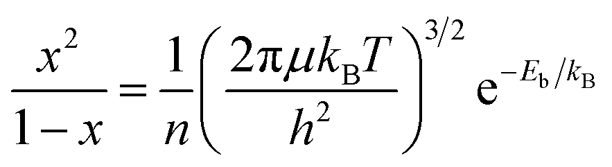 (where x, n, μ, T and h represent the free charge fraction, number of energetic particles, reduced mass of the exciton, temperature and Planck constant respectively),19 the exciton binding energy (Eb), a key parameter for evaluating the strength of the exciton effect, determines the ratio of free charges to excitons at a certain temperature and excitation density.
 | ||
| Fig. 1 Design scheme and structural characterization of s-Ta2O5 NRs. (a) Schematic of typical charge migration and the exciton effect in photocatalysis. (b) Strain-induced charge delocalization endows a delocalized charge transport pathway, minimizing the charge overlap between the electron and hole of the exciton and thus reducing Eb. (c) XRD patterns with an enlarged view of the (001) peak. (d) Raman spectra. (e) Ta 4f orbital XPS spectra. (f) Ta L3-edge XANES spectra. (g) k2-weighted Fourier transform of the EXAFS spectra. (h) Wavelet transform of the k2-weighted EXAFS. | ||
Ambient thermal energy (kBT ≈ 26 meV, where kB is the Boltzmann constant and T is temperature) serves as a critical benchmark for evaluating exciton stability.20 Excitons with Eb above this threshold exhibit greater stability and resistance to dissociation into free charges, whereas those with lower Eb are more susceptible to dissociation. To promote efficient exciton dissociation, researchers exert considerable efforts,9,21–25 such as typically employing charge spatial separation within heterojunctions, creating an internal electric field that reduces Eb and boosts free carrier generation.16,18,26–31 However, due to the significant charge localization inherent in the typical semiconductor catalyst lattice, which often leads to a strong interaction between the electron and hole in the resulting exciton, there are challenges in reducing the Eb below ambient thermal energy. Therefore, developing new strategies to reduce the Eb holds promise for achieving breakthroughs in photocatalytic performance.
Herein, by applying tensile strain to finely adjust charge localization and establish a delocalized transport pathway, we effectively reduce the Eb without relying on external fields or interfaces (Fig. 1b). Taking Ta2O5 as a prototype with exceptional water splitting capability,32–34 we achieved charge delocalization by constructing a tensile strain in Ta2O5 nanorods (s-Ta2O5 NRs). Density functional theory (DFT) calculations further validate that this strain weakens the interaction between Ta 5d and O 2p orbitals, fostering a more delocalized charge transfer channel and significantly increasing the dielectric constant (εr), thereby achieving a reduced Eb. A tensile strain markedly reduces the Eb of s-Ta2O5 NRs to ∼24.26 meV, below the thermal energy at room temperature (kBT, 26 meV), achieving a reduction of 71.50% in comparison to Ta2O5 NRs. This reduction in Eb doubles the carrier lifetime and surface potential, enhancing the separation of photogenerated charges, increasing the yield and separation rate of free charges, and lowering the hydrogen evolution reaction barrier. Consequently, this facilitates direct electron transfer from Ta atoms to protons, markedly boosting photocatalytic hydrogen production, which is 51.5 times higher than that of c-Ta2O5. This study demonstrates that by reducing the exciton binding energy through tensile strain, we can optimize charge transfer and promote photogenerated charge-driven photocatalytic reactions, offering a new avenue for the design and preparation of efficient semiconductor photocatalytic materials.
Results and discussion
Structural characterization of s-Ta2O5 NRs
Herein, the s-Ta2O5 NRs with a tensile strain were successfully fabricated by ingeniously engineering a crystalline/amorphous interface within them, achieved through the strategic insertion of F atoms into the spaces between the vertices of TaO6 octahedra and TaO7 polyhedra. X-ray diffraction (XRD) analysis, as depicted in Fig. 1c and S1,† clearly demonstrates that these s-Ta2O5 NRs (Fig. S2†) exhibit the characteristic orthorhombic Ta2O5, with an evident tensile strain along the [001] axis and an amorphous nature in their orthogonal directions. This was further supported by Raman spectra, which not only confirmed the orthorhombic Ta2O5 phase but also evidenced the presence of tensile strain and a level of crystalline integrity reduction in the s-Ta2O5 NRs (Fig. 1d and Note S1 in the ESI†). Furthermore, X-ray photoelectron spectra (XPS) revealed an increase in the binding energies of the Ta 4f5/2 (28.37 eV) and Ta 4f7/2 orbitals (26.37 eV) in s-Ta2O5 NRs, suggesting an oxidation state beyond the typical +5 state,35 attributed to the F atoms' integration into the matrix (Fig. S3a and c†). Energy-dispersive X-ray spectroscopy (EDS) mapping (Fig. S4†) revealed a uniform distribution of Ta, O, and F elements throughout the nanorods, with a relatively weaker signal for F, indicating its minor presence. XPS quantified the atomic proportions (Fig. S3†) as 20.99% Ta, 52.7% O, and 11.85% F, demonstrating that the s-Ta2O5 NRs not only contain the typical Ta–O bonds but also Ta–F bonds, suggesting a unique interstitial incorporation of F within the lattice, rather than simple substitutional doping. O 1s XPS and electron spin resonance (ESR) measurements (Fig. S3b and S5†) further confirmed the widespread occurrence of oxygen defects.To further elucidate the structural coordination of Ta atoms within s-Ta2O5 NRs, the synchrotron radiation X-ray absorption fine structure (XAFS) spectra were recorded, and compared with those of Ta2O5 NRs (Fig. S6†) and c-Ta2O5 (Fig. S7†). Notably, the X-ray absorption near edge structure (XANES) spectra at the Ta L3 edge show that the s-Ta2O5 NRs display an absorption edge closely aligned with that of the other Ta2O5 samples but with a pronounced white line peak (Fig. 1f), suggesting a slightly higher oxidation state of Ta, potentially beyond +5, consistent with that by Ta 4f XPS spectra. Further, Fourier transform analysis of the extended X-ray absorption fine structure (EXAFS) reveals a dominant peak at approximately 1.48 Å for s-Ta2O5 NRs, indicating a shorter bond length compared to the 1.56 Å Ta–O bond in Ta2O5 NRs and c-Ta2O5, yet longer than the typical Ta–F bond of approximately 1.44 Å, attributed to the presence of Ta–F alongside Ta–O bonds (Fig. 1g). Additionally, this bond length is slightly longer than that observed in typical Ta2O5 samples, yet significantly shorter than the Ta–F bond, indicating a slight increase in coordination number and the incorporation of some fluorine into the s-Ta2O5 NRs lattice (Fig. 1g and S8†). Wavelet transform analysis further distinguishes the s-Ta2O5 NRs by showing similar Ta–O coordination within a 1–3 Å range to other samples, but with enhanced contours at 3–4 Å, indicative of a more distinct separation of Ta atoms, suggesting a degree of disordered structure induced by fluorine incorporation (Fig. 1h). According to the above XAFS results, the insertion of F atoms is inferred to have induced a significant degree of disordered structure within the s-Ta2O5 NRs lattice.
To examine the internal structure and strain of s-Ta2O5 NRs, high-resolution transmission electron microscopy (HRTEM) was performed. The HRTEM image of an individual s-Ta2O5 nanorod (Fig. 2a) clearly shows that it preferentially grows along the [001] axis, with an observed interplanar spacing of the (001) planes slightly increased to about 0.393 nm (Fig. S9†), a subtle yet notable expansion from the 0.388 nm spacing characteristic of the normal Ta2O5 crystal (PDF# 25-0922). Corresponding geometric phase analysis (GPA) further corroborates the presence of a uniform tensile strain of approximately 1.5% along this [001] axis (Fig. 2b). Only a set of bright diffraction spots manifested in the selected area electron diffraction (SAED) pattern (Fig. 2c), which affirms the single-crystal nature of the s-Ta2O5 NRs. Nevertheless, the occurrence of the ‘tail-dragging’ effect in the diffraction signals perpendicular to the [001] direction points to a significant structural disorder in the orthogonal plane. This is evidenced by high-resolution aberration-corrected high-angle annular dark-field (HAADF) scanning TEM images (STEM, Fig. 2d and e), which reveal a multitude of layer faults, including extra and missing atomic layers in the direction orthogonal to the [001]. Further HRTEM investigations (Fig. S10†) on additional s-Ta2O5 nanorods consistently demonstrate the aforementioned tensile strain along the [001] axis and a pronounced disordered structure in the orthogonal plane, consistent with the XRD and Raman spectra analyses.
 | ||
| Fig. 2 Structural characterization of s-Ta2O5 NRs. (a) HRTEM image of the surface. (b) Corresponding eyy strain tensor derived from (a). (c) SAED pattern on the surface. (d) and (e) Aberration-corrected HAADF-STEM images of the surface. (f) Aberration-corrected HAADF-STEM image of the cross-section. (g) and (i) Enlarged views of the areas g and i marked by rectangles in (f), respectively. (h) Corresponding eyy strain tensor of (g). | ||
To explore the atomic arrangement within the (001) plane of these special structured s-Ta2O5 NRs, focused ion beam (FIB) slices were made and then observed by aberration-corrected transmission electron microscopy. The resultant high-resolution HAADF-STEM image taken on the cross-section of an individual s-Ta2O5 nanorod (Fig. 2f and S11a†) clearly delineates a juxtaposition of both ordered and disordered atomic arrangement, alongside a multitude of discernible cavities. A closer inspection of the region labelled as ‘g’ in Fig. 2f clearly exhibits a highly ordered orthorhombic phase Ta2O5 atomic arrangement (Fig. 2g, S11b and S12†), with a slightly larger spacing between (200) planes (∼0.317 nm) compared to the normal Ta2O5 crystal (d(200) ≈ 0.31 nm). The corresponding GPA strain tensor mapping (Fig. 2h) further confirms the presence of a tensile strain of approximately 2% in the [200] direction. In stark contrast, the examination of region ‘i’ in Fig. 2f through an enlarged HAADF-STEM image (Fig. 2i) displays a starkly disordered atomic arrangement, replete with many noticeable cavities, indicative of an amorphous structure. More HAADF-STEM images (Fig. S13†) randomly sampled from the cross-section of another s-Ta2O5 nanorod evidence the repetitive nature of this intricate structural motif, comprising both crystalline and amorphous domains, as well as the consistent occurrence of tensile strain and cavities. Collectively, these observations substantiate that the s-Ta2O5 NRs possess a distinct single-crystal growth pattern along the [001] axis, seamlessly incorporating a blend of ordered and amorphous structures in the perpendicular orientation, and are characterized by the tensile strain within the crystalline regions of Ta2O5, alongside the pervasive presence of cavities.
Ultraviolet absorption and valence band spectra (Fig. S14†) have established s-Ta2O5 NRs as a prototypical semiconductor, with a similar band structure to both Ta2O5 NRs and c-Ta2O5 samples. It manifests a bandgap (Eg) of 4.10 eV, with the valence band maximum (VBM) and the conduction band minimum (CBM) situated at 3.21 eV and −0.89 eV respectively. Theoretical simulations show that F-doping in the Ta2O5 crystal introduces the density of states near the Fermi level that cross the Fermi surface, yielding a metallic band structure (Fig. S15a–c†). However, this contradicts the experimental semiconductor band structure of s-Ta2O5 NRs (Fig. S14†), indicating that F does not contribute to the band structure of s-Ta2O5 NRs. Instead, applying a tensile strain along the [001] axis of the Ta2O5 crystal maintains the semiconductor band structure (Fig. S15d†), with only slight shifts in the band edges, consistent with experimental observations. This suggests that the subtle alterations in the band structure of s-Ta2O5 NRs are mainly attributed to strain effects rather than fluorine doping. These insights, along with the previous TEM, XAS, XPS, XRD, Raman, and EDS analyses, sufficiently verify that the crystal regions under tensile strain consist of pure Ta2O5, while fluorine is mainly located in the amorphous areas. Notably, the orthorhombic Ta2O5 crystal structure is formed by corner-sharing or edge-sharing links between TaO6 octahedra and TaO7 polyhedra, featuring a distinctive interspace at the junction where a TaO6 octahedron and a TaO7 polyhedron share corners (Fig. S16†).36 This interspace, characterized by a lower packing density of oxygen atoms, offers a potential site for F insertion. Given the smaller size and higher electronegativity of F atoms relative to oxygen, they readily occupy these interspaces and form Ta–F bonds, as confirmed by XAS and XPS analyses (Fig. 1e–h and S3†). The insertion of F into the Ta2O5 lattice would push away surrounding atoms, culminating in lattice expansion. This lattice expansion effect instigated by F insertion impacts neighboring Ta2O5 crystalline regions, engendering tensile strain. Consequently, the synthesized s-Ta2O5 NRs exhibit an ordered growth along the [001] direction, alternating between pure Ta2O5 crystalline regions and F-doped amorphous areas, containing tensile strain and associated cavities.
Notably, although Ta2O5 NRs maintain the same size and morphology as the s-Ta2O5 NRs after annealing at 750 °C (Fig. S6†), their XRD pattern and Raman spectrum (Fig. 1c and d) indicate that the tensile strain disappears. Furthermore, HRTEM images, captured with the electron beam directed along various axes of the Ta2O5 NR (Fig. S17†), display well-defined lattice fringes consistent with the orthorhombic Ta2O5 crystal structure. This is supported by the presence of sharp diffraction spots, free of the tail-dragging effect, in the corresponding FFT images, suggesting a well-crystallized single-crystal structure. GPA strain tensor mapping further verifies the absence of strain in the Ta2O5 NRs (Fig. S18†). After annealing, fluorine is eliminated (Fig. 1g and S3†), and the previously fluorine-doped Ta2O5 amorphous regions are converted into an ordered crystalline pure Ta2O5 phase (Fig. 1c, d, S3, S6, and S17†), resulting in the removal of tensile strain. Evidently, the creation of localized amorphous regions is the primary cause of the tensile strain in s-Ta2O5 NRs.
Effect of tensile strain on Eb in s-Ta2O5 NRs
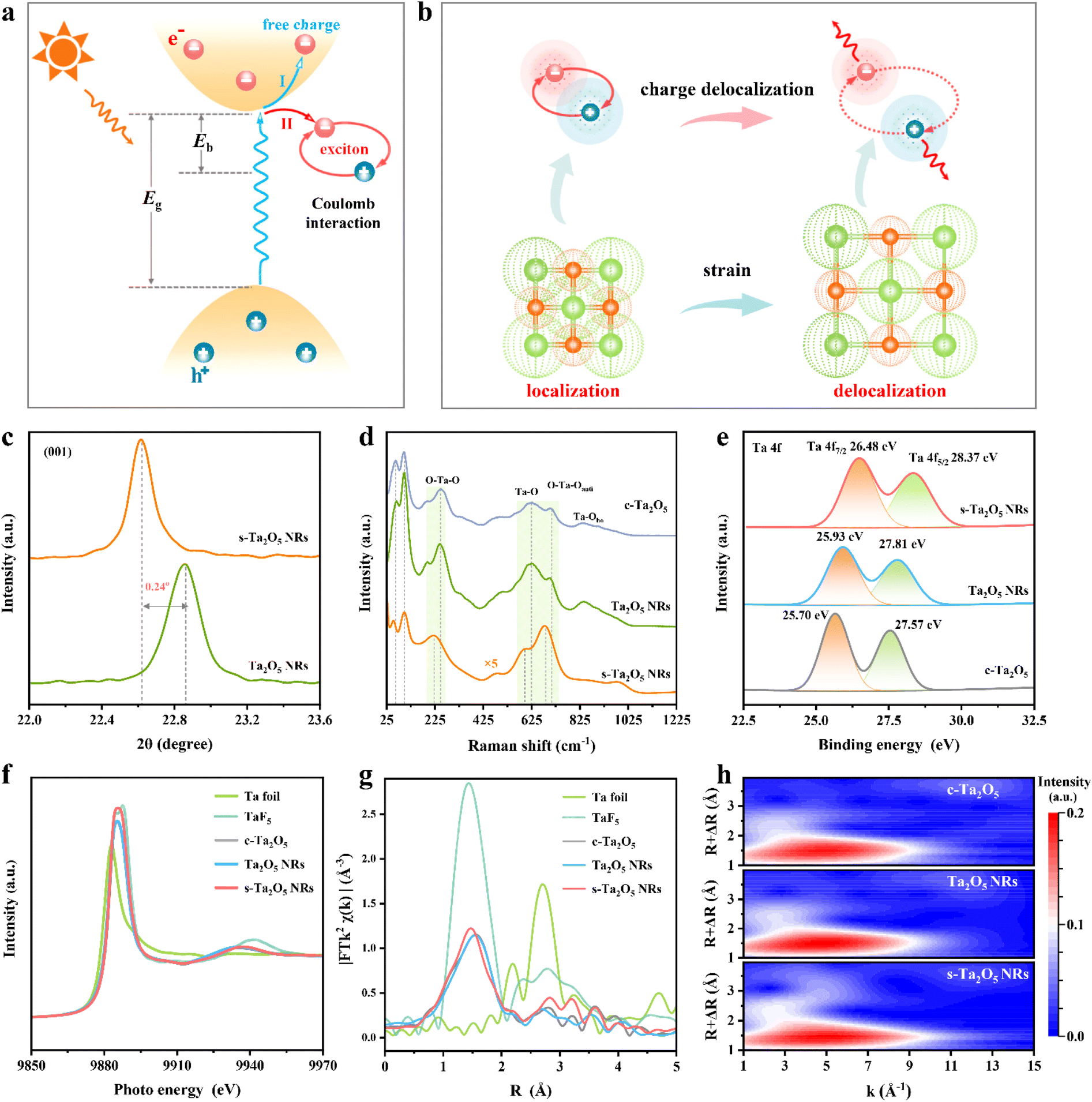
To evaluate the effect of tensile strain on Eb, temperature-dependent photoluminescence (PL) spectroscopy was meticulously performed. The PL spectra from all samples (Fig. 3a–c) exhibit a consistent increase in PL peak intensity as the temperature decreases, attributable to phonon-assisted relaxation. Accordingly, the Eb values for various Ta2O5 samples were determined by employing the Arrhenius equation IT = I0/(1 + A exp(−Eb/kBT)) to fit the acquired PL data (Fig. 3d and S19†).18 As stated within semiconductor physics, a reduction in size would weaken the dielectric screening effect, thereby increasing the exciton effect.15,37,38 Indeed, Ta2O5 NRs exhibit a larger Eb of 85.15 meV compared to c-Ta2O5, which has an Eb of 38.37 meV (Fig. 3e).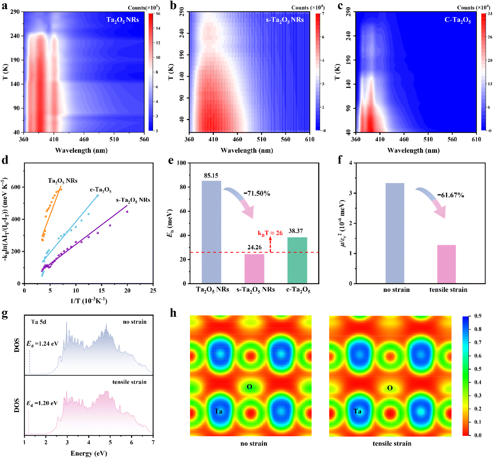 | ||
| Fig. 3 The effect of tensile strain on the Eb of s-Ta2O5 NRs. Temperature-dependent PL spectra of (a) Ta2O5 NRs, (b) s-Ta2O5 NRs and (c) c-Ta2O5. (d) Integrated PL emission intensity as a function of temperature. (e) Comparative Eb values for s-Ta2O5 NRs, Ta2O5 NRs, and c-Ta2O5. (f) Calculated μ/εr2 values. (g) Ta 5d PDOS and corresponding d-band centers. (h) ELF plots for Ta2O5 without (left) and with (right) a tensile strain along [001]. | ||
However, introducing tensile strain results in a substantial decrease in the Eb for s-Ta2O5 NRs (which have the same size and morphology as Ta2O5 NRs, Fig. S2 and S6†) to 24.26 meV, which is significantly lower than that of both the unstrained Ta2O5 NRs and c-Ta2O5 samples, and even below ambient thermal energy (kBT ≈ 26 meV), suggesting an easy dissociation of excitons into free charges during photocatalysis. According to the equation Eb = μE0/m0εr2, Eb is predominantly determined by the variables μ and εr.39,40 To further examine the effect of strain on Eb, the μ and εr values for Ta2O5 crystal models (Fig. S20†), both with and without a tensile strain along the [001] direction, were calculated (Fig. S21†). Fig. 3f illustrates that a tensile strain along the [001] direction markedly causes a 61.67% decrease in the value of μ/εr2, aligning well with the experimentally observed trends in Eb variation. Both experimental and theoretical results robustly support the assertion that tensile strain can significantly lower the Eb in Ta2O5 photocatalysts, which in turn weakens the coulombic interaction between photoexcited electrons and holes, enhancing charge separation efficiency, liberating more free charges, and promoting charge-driven photocatalytic reactions.
To explore the effect of tensile strain on Eb, we performed DFT calculations to assess the density of states (DOS) and electron localization function (ELF) in Ta2O5, both with and without the application of tensile strain. The d-band center theory offers an effective method for evaluating the bonding conditions in transition metals.41–43 As illustrated in Fig. 3g, there is a discernible reduction in the partial density of states (PDOS) for Ta 5d above the Fermi level. Concurrently, there is a slight shift in the d-band center (Ed) from 1.24 eV to 1.20 eV. These observations, combined with the O 2p PDOS (Fig. S22†) suggest that tensile strain could weaken the antibonding interactions between Ta and O atoms, consequently decreasing the overlap between the Ta 5d and O 2p orbitals. The ELF offers an effective description of electron delocalization in solids,44,45 serving as a valuable tool for the chemical bonds' classification.46,47 Further scrutiny of the ELF contour plots on the (001) crystal plane (Fig. 3h and S23†) reveals a reduction in ELF values near oxygen atoms under a tensile strain along the [001] axis, indicating a lower charge density and increased electron delocalization in these areas. These observations collectively imply that tensile strain reduces the interaction between Ta 5d and O 2p orbitals, promoting a more delocalized pathway for efficient charge transport.48 This, in turn, lessens the coulombic interaction between photoexcited electrons and holes in excitons, thereby lowering the Eb.
Effect of tensile strain on charge transport
Reducing Eb facilitates the separation of photoexcited charge carriers, providing more free charge carriers for the photocatalytic reactions. To confirm this point, the influence of tensile strain on the charge transport was studied using Kelvin probe force microscopy (KPFM). Fig. 4a and b reveal that the surface potential of s-Ta2O5 NRs is considerably two times higher than that for unstrained Ta2O5 NRs, suggesting a lower work function and Fermi level, which are conducive to electron separation. Moreover, the influence of tensile strain on the lifetime of photo-generated charge carriers was further investigated using advanced time-resolved PL spectroscopy. In Fig. 4c, the PL lifetime of the s-Ta2O5 NRs reaches up to 2.18 ns, notably surpassing that for both Ta2O5 NRs (1.19 ns) and c-Ta2O5 (1.94 ns). This is indicative of the tensile strain’s efficacy in diminishing electron–hole recombination rates within the s-Ta2O5 NRs, in line with the observed trend in the reduction of Eb. In parallel, electrochemical impedance spectra (EIS) provided additional evidence, where the s-Ta2O5 NRs exhibit the smallest semicircle in the Nyquist plots (Fig. 4d), signifying exceptional charge transfer capabilities and the most efficient charge migration when benchmarked against Ta2O5 NRs and c-Ta2O5. Collectively, these experimental results robustly validate that the introduction of tensile strain substantially diminishes exciton binding energy, thereby extending the lifetime of photo-generated charges and promoting effective charge separation and migration, which is highly beneficial for photogenerated charge-involved photocatalytic reactions. | ||
| Fig. 4 The effect of tensile strain on charge transport in s-Ta2O5 NRs. Atomic force microscopy images (left) and the corresponding surface potentials measured with KPFM (right) of (a) Ta2O5 NRs and (b) s-Ta2O5 NRs. (c) Time-resolved transient PL decay. (d) EIS spectra. | ||
Photocatalytic activity
To validate that tensile strain-induced decrease in Eb can be leveraged to substantially promote charge separation, photocatalytic water splitting was further evaluated. Hydrogen production from photocatalytic water splitting using s-Ta2O5 NRs under ultraviolet illumination in a methanol/water solution was conducted and compared with that of Ta2O5 NRs and c-Ta2O5. Fig. 5a exhibits a direct proportional relationship between the duration of light illumination and the amount of hydrogen evolved, indicating a consistent photocatalytic activity over various Ta2O5 samples. Notably, s-Ta2O5 NRs achieve a hydrogen production rate of 69.24 μmol h−1, significantly surpassing that of Ta2O5 NRs (3.98 μmol h−1) and c-Ta2O5 (1.32 μmol h−1), representing an increase by approximately 16.4 and 51.5 times, respectively (Fig. 5b). No hydrogen was detected in the absence of either irradiation or photocatalysts, suggesting H2 production solely attributable to the photocatalytic reaction on the Ta2O5 catalysts. The s-Ta2O5 NRs demonstrate a steady linear rise in hydrogen production over five consecutive cycles (Fig. 5c), indicating robust catalytic activity and stability. Subsequent SEM and XRD analyses post-catalysis show no notable changes in the morphology or crystal structure (Fig. S24†), corroborating the structural integrity of s-Ta2O5 NRs throughout the photocatalytic reaction. The structural characterization above suggests that s-Ta2O5 NRs have comparable structure sizes (the specific surface areas of s-Ta2O5 NRs and Ta2O5 NRs were measured at approximately 15.8 and 11.9 m2 g−1 respectively) and nearly identical energy bands to Ta2O5 NRs. Moreover, no significant hydrogen was detected when both F-doped and undoped amorphous Ta2O5 samples were used as catalysts. Additionally, the F element is solely found in the amorphous region in s-Ta2O5 NRs; these areas will not be involved in photo-excitation and production of photogenerated charges. Taken together, these results emphatically validate that the resultant tensile strain in s-Ta2O5 NRs effectively decreases exciton binding energy, thereby enhancing charge separation and ultimately leading to an exceptional enhancement of photocatalytic activity. | ||
| Fig. 5 Photocatalytic water splitting performances and mechanism of s-Ta2O5 NRs. (a) Photocatalytic H2 production from water splitting for s-Ta2O5 NRs, Ta2O5 NRs, and c-Ta2O5 under UV light irradiation. (b) Comparative photocatalytic hydrogen evolution rates for s-Ta2O5 NRs, Ta2O5 NRs, and c-Ta2O5, respectively. (c) Repeated hydrogen generation performance of s-Ta2O5 NRs. In situ ESR spectra of (d) DMPO-trapped ˙O2− radicals and (e) TEMPO-trapped h+ in s-Ta2O5 NRs. (f) Gibbs free energy diagram for H2 production through water splitting. (g) Charge density difference of H on Ta2O5 with a tensile strain along the [001] direction. The isosurface level is 0.00025 au. The yellow and blue shadows indicate charge accumulation and depletion, respectively. (h) Corresponding slice image of (g) across the (010) face. (i) PDOS of H 1s, Ta 5d, O 2p orbitals with H adsorbed on Ta2O5 with a tensile strain along the [001] direction. | ||
To delve into the underlying photocatalytic mechanisms, in situ ESR spectroscopy was employed to monitor the reactive species throughout the photocatalytic process. 2,2,6,6-Tetramethyl-1-piperidinyloxy (TEMPO) and 5,5-dimethyl-1-pyrroline-N-oxide (DMPO) radicals as scavengers were utilized for the direct observation of photogenerated holes and superoxide radicals (˙O2−) respectively. The DMPO signal, absent under dark conditions, markedly increases with light exposure and continues to rise over time (Fig. 5d), indicating a steady production of photogenerated electrons. This is further corroborated by the detection of photogenerated ˙OH (Fig. S25†). In contrast, the TEMPO signal diminishes when exposed to light and further decreases with prolonged illumination (Fig. 5e), suggesting the sustained formation and accumulation of photogenerated holes. Further, DFT calculations reveal that the tensile strain can lower the Gibbs free energy for hydrogen production, thereby lowering the energy barrier for both water molecule adsorption and hydrogen gas release (Fig. 5f), facilitating the water-splitting reaction. Charge density difference calculation shows a reduced charge on Ta atoms and a heightened charge around H atoms, indicating a direct electron transfer from Ta to H atoms (Fig. 5g and h). PDOS analysis further confirmed a robust interaction between Ta 5d and H 1s orbitals (Fig. 5i). Integrating ESR analyses with DFT calculations, it is inferred that the introduction of tensile strain significantly lowers Eb, endows a strong interaction between Ta 5d and H 1s orbitals, and reduces the Gibbs free energy of hydrogen production, thereby facilitating efficient electron transfer for water reduction and hydrogen generation, as well as sustaining photogenerated holes for the photocatalytic oxidation reactions.
Conclusions
In summary, we have successfully fabricated s-Ta2O5 single crystal nanorods with tensile strain by ingeniously engineering a crystalline/amorphous interface within them through the strategic insertion of F atoms into the interspaces shared by the vertices of TaO6 octahedra and TaO7 polyhedra. This strain weakens the interaction between Ta 5d and O 2p orbitals in s-Ta2O5 NRs, thereby reducing charge localization and building a more delocalized charge transport channel. This significantly decreases the Eb to below ambient thermal energy (∼26 meV), marking a 71.50% decrease compared to their unstrained counterparts. A lower Eb contributes to enhanced carrier lifetime and surface potential, improved charge separation efficiency, and a lowered hydrogen evolution reaction barrier, thereby endowing direct electron transfer from Ta atoms to protons. As a result, the s-Ta2O5 NRs exhibit a markedly improved photocatalytic hydrogen production activity, with generation rates surpassing those of Ta2O5 NRs and c-Ta2O5 by 16.4 and 51.5 times, respectively. The study not only offers an effective strategy to reduce exciton binding energy through strain-induced charge delocalization, but also paves a novel avenue for the design of highly efficient photoconversion systems.Data availability
All experimental procedures, computational sections, and associated data are included in the article and ESI.†Author contributions
J. D., Y. L., and T. Z. conceived and directed the project. J. D. designed and executed the experiments. J. D. and Y. L. co-wrote the paper. J. D., Y. W., Y. Z., and Y. L. performed and analyzed the DFT calculations. J. D. and Y. L. conducted and interpreted the XAFS spectroscopy. J. D. and C. L. collaboratively conducted PL. J. D., J. H., and Y. Z. jointly performed AFM and KPFM. J. D. and D. Z. carried out and discussed the GPA. J. D., Y. L., X. J., J. G., and T. Z. revised the paper. J. C. participated in the discussion of the catalytic mechanism. All authors discussed the results and contributed to the manuscript preparation.Conflicts of interest
The authors declare no competing financial interest.Acknowledgements
This work was financially supported by the National Natural Science Foundation of China (22071069, 22173048, and 22103026), the Project Funded by the China Postdoctoral Science Foundation (2019M662604), and the Scientific Research Fund Project of Wuhan Institute of Technology (no. 23QD06). We thank the Analytical and Testing Center at Huazhong University of Science and Technology for their technical support, especially Dr Jianquan Zhao. We also acknowledge the support of the HPC platform at HUST. Furthermore, the authors greatly appreciate the beam time allocation and assistance provided by beamline BL11B at the Shanghai Synchrotron Radiation Facility.References
- T. Hisatomi and K. Domen, Nat. Catal., 2019, 2, 387–399 CrossRef CAS.
- W. H. Lee, C. W. Lee, G. D. Cha, B.-H. Lee, J. H. Jeong, H. Park, J. Heo, M. S. Bootharaju, S.-H. Sunwoo, J. H. Kim, K. H. Ahn, D.-H. Kim and T. Hyeon, Nat. Nanotechnol., 2023, 18, 754–762 CrossRef CAS PubMed.
- X. P. Tao, Y. Zhao, S. Y. Wang, C. Li and R. G. Li, Chem. Soc. Rev., 2022, 51, 3561–3608 RSC.
- J. Y. Y. Loh, N. P. Kherani and G. A. Ozin, Nat. Sustainability, 2021, 4, 466–473 CrossRef.
- S. P. Che, J. H. Zhang, F. Z. Mou, X. Guo, J. E. Kauffman, A. Sen and J. G. Guan, Research, 2022, 2022, 9816562 CrossRef CAS PubMed.
- M. Z. Li, J. Z. Wang, Q. Y. Wang, H. L. Lu, G. F. Wang and H. G. Fu, Chem. Sci., 2024, 15, 1860–1869 RSC.
- P. Zhou, I. A. Navid, Y. Ma, Y. Xiao, P. Wang, Z. Ye, B. Zhou, K. Sun and Z. Mi, Nature, 2023, 613, 66–70 CrossRef PubMed.
- J. Y. Duan, G. Y. Mou, S. Zhang, S. Wang and J. G. Guan, J. Mater. Chem. A, 2015, 3, 14686–14695 RSC.
- Q. Wang, C. Pornrungroj, S. Linley and E. Reisner, Nat. Energy, 2022, 7, 13–24 CrossRef.
- B. Jin, N. Zuo, Z. Y. Hu, W. J. Cui, R. Y. Wang, G. Van Tendeloo, X. Zhou and T. Y. Zhai, Adv. Funct. Mater., 2020, 30, 2006166 CrossRef.
- H. Wang, W. X. Liu, X. He, P. Zhang, X. D. Zhang and Y. Xie, J. Am. Chem. Soc., 2020, 142, 14007–14022 CrossRef PubMed.
- S. Kang, K. Kim, B. H. Kim, J. Kim, K. I. Sim, J. U. Lee, S. Lee, K. Park, S. Yun, T. Kim, A. Nag, A. Walters, M. Garcia-Fernandez, J. Li, L. Chapon, K. J. Zhou, Y. W. Son, J. H. Kim, H. Cheong and J. G. Park, Nature, 2020, 583, 785–789 CrossRef PubMed.
- Q. C. Burlingame, X. Liu, M. L. Ball, B. P. Rand and Y. L. Loo, Energy Environ. Sci., 2023, 16, 1742–1751 RSC.
- J. Pradhan, A. Das, K. Kundu, Chahat and K. Biswas, Chem. Sci., 2022, 13, 9952–9959 RSC.
- P. Chen, T. L. Atallah, Z. Y. Lin, P. Q. Wang, S. J. Lee, J. Q. Xu, Z. H. Huang, X. D. Duan, Y. Ping, Y. Huang, J. R. Caram and X. F. Duan, Nature, 2021, 599, 404–410 CrossRef CAS PubMed.
- Y. Qian, Y. Han, X. Zhang, G. Yang, G. Zhang and H.-L. Jiang, Nat. Commun., 2023, 14, 3083 CrossRef CAS.
- C. Li, J. Liu, H. Li, K. Wu, J. Wang and Q. Yang, Nat. Commun., 2022, 13, 2357 CrossRef CAS.
- Z.-A. Lan, G. Zhang, X. Chen, Y. Zhang, K. A. I. Zhang and X. Wang, Angew. Chem., Int. Ed., 2019, 58, 10236–10240 CrossRef CAS.
- M. B. Price, P. A. Hume, A. Ilina, I. Wagner, R. R. Tamming, K. E. Thorn, W. T. Jiao, A. Goldingay, P. J. Conaghan, G. Lakhwani, N. Davis, Y. F. Wang, P. Y. Xue, H. Lu, K. Chen, X. W. Zhan and J. M. Hodgkiss, Nat. Commun., 2022, 13, 2827 CrossRef CAS.
- M. H. Huang, S. Mao, H. Feick, H. Q. Yan, Y. Y. Wu, H. Kind, E. Weber, R. Russo and P. D. Yang, Science, 2001, 292, 1897–1899 CrossRef CAS.
- A. Raja, L. Waldecker, J. Zipfel, Y. Cho, S. Brem, J. D. Ziegler, M. Kulig, T. Taniguchi, K. Watanabe, E. Malic, T. F. Heinz, T. C. Berkelbach and A. Chernikov, Nat. Nanotechnol., 2019, 14, 832–837 CrossRef CAS PubMed.
- Y. Lei, Y. Li, C. Lu, Q. Yan, Y. Wu, F. Babbe, H. Gong, S. Zhang, J. Zhou, R. Wang, R. Zhang, Y. Chen, H. Tsai, Y. Gu, H. Hu, Y.-H. Lo, W. Nie, T. Lee, J. Luo, K. Yang, K.-I. Jang and S. Xu, Nature, 2022, 608, 317–323 CrossRef CAS.
- A. Raja, A. Chaves, J. Yu, G. Arefe, H. M. Hill, A. F. Rigosi, T. C. Berkelbach, P. Nagler, C. Schueller, T. Korn, C. Nuckolls, J. Hone, L. E. Brus, T. F. Heinz, D. R. Reichman and A. Chernikov, Nat. Commun., 2017, 8, 15251 CrossRef.
- Y. B. Shi, J. Li, C. L. Mao, S. Liu, X. B. Wang, X. F. Liu, S. X. Zhao, X. Liu, Y. Q. Huang and L. Z. Zhang, Nat. Commun., 2021, 12, 5923 CrossRef CAS PubMed.
- N. Kornienko, J. Z. Zhang, K. K. Sakimoto, P. D. Yang and E. Reisner, Nat. Nanotechnol., 2018, 13, 890–899 CrossRef CAS PubMed.
- B. Wu, J. Z. Fan, J. Y. Han, Y. Su, M. P. Zhuo, J. H. Sun, Y. Gao, S. Chen, J. J. Wu, Z. S. Wang and X. D. Wang, Adv. Mater., 2023, 35, 2206272 CrossRef CAS.
- J. Kosco, S. Gonzalez-Carrero, C. T. Howells, T. Fei, Y. F. Dong, R. Sougrat, G. T. Harrison, Y. Firdaus, R. Sheelamanthula, B. Purushothaman, F. Moruzzi, W. D. Xu, L. Y. Zhao, A. Basu, S. De Wolf, T. D. Anthopoulos, J. R. Durrant and I. McCulloch, Nat. Energy, 2022, 7, 340–351 CrossRef CAS.
- A. Ciarrocchi, F. Tagarelli, A. Avsar and A. Kis, Nat. Rev. Mater., 2022, 7, 449–464 CrossRef.
- S. Nishioka, K. Hojo, L. Xiao, T. Gao, Y. Miseki, S. Yasuda, T. Yokoi, K. Sayama, T. E. Mallouk and K. Maeda, Sci. Adv., 2022, 8, eadc9115 CrossRef CAS PubMed.
- J. V. Passarelli, C. M. Mauck, S. W. Winslow, C. F. Perkinson, J. C. Bard, H. Sai, K. W. Williams, A. Narayanan, D. J. Fairfield, M. P. Hendricks, W. A. Tisdale and S. I. Stupp, Nat. Chem., 2020, 12, 672–682 CrossRef CAS PubMed.
- F. Li, Z. H. Fang, Z. H. Xu and Q. J. Xiang, Energy Environ. Sci., 2024, 17, 497–509 RSC.
- V. Gurylev, Mater. Today Sustainability, 2022, 18, 100131 CrossRef.
- P. Zhang, J. J. Zhang and J. L. Gong, Chem. Soc. Rev., 2014, 43, 4395–4422 RSC.
- Z. Wang, Y. Inoue, T. Hisatomi, R. Ishikawa, Q. Wang, T. Takata, S. Chen, N. Shibata, Y. Ikuhara and K. Domen, Nat. Catal., 2018, 1, 756–763 CrossRef.
- M. A. Lange, I. Khan, P. Opitz, J. Hartmann, M. Ashraf, A. Qurashi, L. Praedel, M. Panthoefer, A. Cossmer, J. Pfeifer, F. Simon, M. von der Au, B. Meermann, M. Mondeshki, M. N. Tahir and W. Tremel, Adv. Mater., 2021, 33, 2007434 CrossRef PubMed.
- Y. Yang and Y. Kawazoe, Phys. Rev. Mater., 2018, 2, 034602 CrossRef.
- Y. Zhang, F. K. Wang, X. Feng, Z. Zhang, K. L. Liu, F. F. Xia, W. X. Liang, X. Z. Hu, Y. Ma, H. Q. Li, G. C. Xing and T. Y. Zhai, Adv. Funct. Mater., 2022, 32, 2205757 CrossRef.
- L. K. Li, J. Kim, C. H. Jin, G. J. Ye, D. Y. Qiu, F. H. da Jornada, Z. W. Shi, L. Chen, Z. C. Zhang, F. Y. Yang, K. Watanabe, T. Taniguchi, W. Ren, S. G. Louie, X. H. Chen, Y. B. Zhang and F. Wang, Nat. Nanotechnol., 2017, 12, 21–25 CrossRef PubMed.
- M. Baranowski and P. Plochocka, Adv. Energy Mater., 2020, 10, 1903659 CrossRef.
- A. Miyata, A. Mitioglu, P. Plochocka, O. Portugall, J. T. W. Wang, S. D. Stranks, H. J. Snaith and R. J. Nicholas, Nat. Phys., 2015, 11, 582–587 Search PubMed.
- N. Hong Nhan, T. Reier, H.-S. Oh, M. Gliech, P. Paciok, V. Thu Ha Thi, D. Teschner, M. Heggen, V. Petkov, R. Schloegl, T. Jones and P. Strasser, Nat. Catal., 2018, 1, 841–851 Search PubMed.
- K. Jia, J. Ma, J. Wang, Z. Liang, G. Ji, Z. Piao, R. Gao, Y. Zhu, Z. Zhuang, G. Zhou and H.-M. Cheng, Adv. Mater., 2023, 35, 2208034 CrossRef.
- H. Yang, C. L. Dong, H. M. Wang, R. J. Qi, L. Q. Gong, Y. R. Lu, C. H. He, S. H. Chen, B. You, H. F. Liu, J. L. Yao, X. L. Jiang, X. P. Guo and B. Y. Xia, Proc. Natl. Acad. Sci. U. S. A., 2022, 119, e2202812119 CrossRef.
- A. Savin, R. Nesper, S. Wengert and T. F. Fassler, Angew. Chem., Int. Ed., 1997, 36, 1809–1832 CrossRef.
- X. Feng, K. J. Bu, T. Liu, S. H. Guo, Z. D. Sun, T. H. Fu, Y. S. Xu, K. L. Liu, S. J. Yang, Y. H. Zhao, H. Q. Li, X. J. Lu and T. Y. Zhai, Angew. Chem., Int. Ed., 2022, 62, e202217238 CrossRef.
- D. B. Chesnut and A. Savin, J. Am. Chem. Soc., 1999, 121, 2335–2336 CrossRef.
- B. Silvi and A. Savin, Nature, 1994, 371, 683–686 CrossRef.
- J. Y. Duan, T. Y. Liu, Y. H. Zhao, R. O. Yang, Y. Zhao, W. B. Wang, Y. W. Liu, H. Q. Li, Y. F. Li and T. Y. Zhai, Nat. Commun., 2022, 13, 2039 CrossRef.
Footnotes |
| † Electronic supplementary information (ESI) available. See DOI: https://doi.org/10.1039/d4sc05873a |
| ‡ These authors contributed equally to this work. |
| This journal is © The Royal Society of Chemistry 2024 |