A review on passivation engineering for improving photocatalytic hydrogen evolution performance
Dandan
Ma
 ,
Jiantao
Chen
,
Jun
Li
,
Xin
Ji
and
Jian-Wen
Shi
,
Jiantao
Chen
,
Jun
Li
,
Xin
Ji
and
Jian-Wen
Shi
 *
*
State Key Laboratory of Electrical Insulation and Power Equipment, Center of Nanomaterials for Renewable Energy, School of Electrical Engineering, Xi'an Jiaotong University, Xi'an 710049, China. E-mail: jianwen.shi@mail.xjtu.edu.cn
First published on 15th April 2024
Abstract
Photocatalytic hydrogen evolution (PHE) is a promising route for the energy-renewable and eco-friendly development of the future society, but the low activity and durability of photocatalysts seriously restrict the development of this technology. In this case, passivation engineering may provide a feasible idea to solve these problems, by which a relatively stable and mild environment can be formed to guarantee the high separation and utilization of photogenerated charge carriers. Recently, passivation engineering has been increasingly adopted for improving the activity and durability of photocatalysts, and thus, a comprehensive review will help researchers understand and use this technology to construct high-performance photocatalytic systems. Herein, firstly, the basic concept and the roles of the passivation technique in PHE are discussed. Subsequently, we introduce the commonly utilized synthesis methods, followed by the characterization techniques employed in passivation engineering. Thereafter, we review the categories and mechanism of passivation engineering in PHE. Lastly, the challenges and perspectives of passivation engineering for future practical applications are discussed. We hope that this review can provide some useful guidance and trigger interest in passivation engineering for the construction of high-performance photocatalysts.
1. Introduction
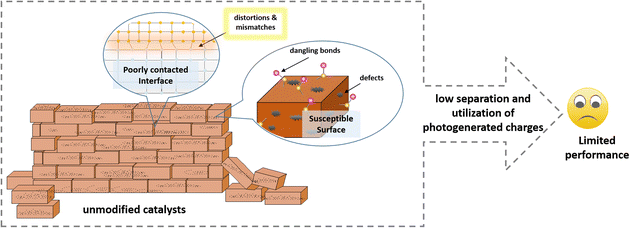
The development of sustainable energy is the focus of attention worldwide. In this case, photocatalytic hydrogen evolution (PHE) technology is capable of converting endless solar energy into clean hydrogen and thus is promising for driving the development and revolution of sustainable energy.1–4 The key to the practical development and application of PHE technology is to find ideal photocatalysts that can efficiently and stably convert solar energy into hydrogen.5,6 Many photocatalysts, such as single-component semiconductors (ZnO, TiO2, CdS, ZnS, MoS2, g-C3N4, etc.7–15) and hybrid systems consisting of two or three semiconductors (TiO2@ZnO, CdS@g-C3N4, CdS/MoS2, etc.16–22) have been reported to date. However, their limited photocatalytic activity and unsatisfactory stability are still the most significant issues.16–19 The core task of developing high-performance photocatalysts is to suppress the harmful recombination of charge carriers, accelerate the surface reaction and prevent photocorrosion.Accordingly, massive efforts, including morphological and structural design, ion doping, homojunction and heterojunction construction, and single atomic modification strategies,23–27 have been devoted to improving the light absorption, charge transfer and surface reaction of photocatalysts in the past decades. However, an unshakable fact is that the use of each of the mentioned strategies often introduces new problems while solving one problem, thus failing to significantly improve the properties of the catalyst as expected. For example, single-component semiconductor photocatalysts suffer from serious charge recombination, which can be solved through the construction of a heterostructure, but the inadequate interface contact between different semiconductors results in harmful charge carrier recombination at the interface. Another example is that increasing the specific surface area of catalysts can undoubtedly provide more active sites for the hydrogen evolution reaction, but the exposure of these susceptible surfaces also results in more serious photocorrosion and more side reactions. Fortunately, this compensatory improvement in the performance of photocatalysts has been noticed by researchers, and they are actively looking for ways to establish a better balance to minimize potential negative impacts.
Among the numerous strategies, passivation technique may provide one of the most ideal solutions to the mentioned problems.28,29 The passivation technique can be used to reduce the effect of photogenerated holes on the catalyst surface or provide additional protection for sensitive catalyst surfaces.30–32 In other reports, passivation techniques can also release the stress between different semiconductors to guarantee the formation of high-quality interfaces.33,34 However, to the best of our knowledge, there are scarce reviews thoroughly summarizing the application of the passivation technique in PHE although this topic has been gaining continuous attention. This was a positive incentive for us to provide a comprehensive review to introduce the basic principle and recent progress in the passivation technique, which may provide ideas and design inspiration for researchers to further improve the activity and stability of photocatalysts.
This review aims to provide a panorama of passivation engineering over semiconductor-based composite photocatalysts and systematically summarize the progress in different passivation strategies in recent years. Initially, we present a brief introduction to the basic concept and the roles of passivation technique in PHE. Subsequently, we introduce the commonly utilized synthesis methods and characterization methods in passivation engineering. Then, we review the categories and mechanism of passivation engineering in PHE. Finally, the challenges and perspectives of passivation engineering for future practical applications are discussed.
2. The basic principles and roles of passivation engineering in PHE
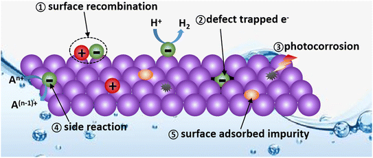
Passivation is a material treatment method developed in the metal materials field, which initially refers to the phenomenon that after forming a thin layer of metal oxide on the surface of the active metal, the protection effect of the metal oxide makes it difficult for the inner metal to be further oxidized, thus displaying inert chemical properties.35,36 Therefore, the direct role of the passivation technique is to shield the active and easily affected factors in the original system or remove them to improve the stability of the system.As is known, catalytic reactions occur in dynamic and easily disturbed systems. As shown in Fig. 1, the continuous generation of electrons and holes, the unstable solid–liquid and solid–solid interfaces, the large exposure of active surface, and the presence of defects and vacancies create an environment in which the photocatalyst itself is easily destroyed by photocorrosion and the photogenerated charge carriers are easily quenched.37,38 (1) The surface photogenerated holes and electrons may undergo harmful recombination before the REDOX reaction. (2) The PHE will decrease if the photogenerated electrons are trapped and quenched by defects. (3) The lifetime of photocatalysts will decrease due to photo-corrosion. (4) The competing side reactions consume electrons, resulting in a limited PHE performance. (5) The PHE activity can also be affected by the impurities adsorbed on the surface of photocatalysts. Thus, passivation engineering in PHE can be employed to prolong the service life of photocatalysts and improve their hydrogen evolution capacity by eliminating the above-mentioned potential negative factors.
2.1 Prolonging the service life of photocatalysts
Photo-corrosion is a long-term problem, where some light-sensitive photocatalysts will dissolve or undergo structural changes under light irradiation conditions, and thus lose their catalytic activity rapidly.39–41 In this case, a passivation layer can provide extra protection to the light-sensitive component, suppress the corrosion reaction at the solid–liquid interface and reduce the instability of the solid–solid interface. In addition, the introduction of a passivation layer can create an inert environment to prevent the occurrence of adverse surface reactions and provide a relatively stable platform for the evolution of hydrogen, thus prolonging the lifetime of the photocatalyst (Fig. 2).42,432.2 Improving hydrogen evolution activity
Besides the accessible surface of the photocatalyst, its complex inner environment can also be improved by passivation techniques. During the past few decades, many researchers have focused on decreasing the harmful defects, vacancies, and interface disorders to suppress the recombination of charge carriers.44,45 The passivation technique has been proven to be efficient in inhibiting the formation of harmful defects and releasing interface stress, thus creating a smooth channel for the transfer of photogenerated charge carriers from the inner to the surface reaction sites of the catalyst.46,473. Realization of passivation engineering
When passivation engineering is used to improve the activity and lifetime of a photocatalyst, it is necessary to carefully design and tailor it to create a stable and unobstructed reaction environment and minimize the potential negative impact of passivation engineering on the catalyst. Among the factors, the choice of an appropriate synthesis method plays the dominant role in guaranteeing the passivation effect. Here, the most commonly utilized synthesis methods will be introduced and discussed.3.1 In situ reaction method
The in situ fabrication method is a widely used strategy in inserting a passivation layer between two different materials. For example, Dey and coworkers48 fabricated a Cu2O/CuO heterojunction using an atmospheric pressure plasma jet method (Fig. 3a), and in this process, CuO with a low density of interfacial defects can be formed from the surface of the Cu2O base, and thus an intimately contacted heterostructure can be constructed. The catalytic performance and stability of the Cu2O photocatalyst were significantly enhanced with the treatment plasma. Daskalakis and coworkers49 treated a Cu-doped ZnS photocatalyst using a wet-chemical sulfidation process and obtained Cu2S in the system (Fig. 3b). It was found that on a particular composite catalyst, the surface defect sites of Cu-ZnS can be passivated during the sulfidation process, in which sulfur vacancies were created from the charge compensation by Cu+ substitution with Zn2+ sites, leading to improved charge transfer at the Cu2S/ZnS interface, and thus the photocatalytic activity of Cu-ZnS could be largely improved. In addition, Alam et al.50 passivated g-C3N4-S by loading BiOI nanoplates with carbon nitride structures through an in situ hydrothermal method (Fig. 3c). They found that the synergistic effect of trap passivation and charge separation in g-C3N4-S/BiOI efficiently resulted in a higher photocurrent and lower charge transfer resistance.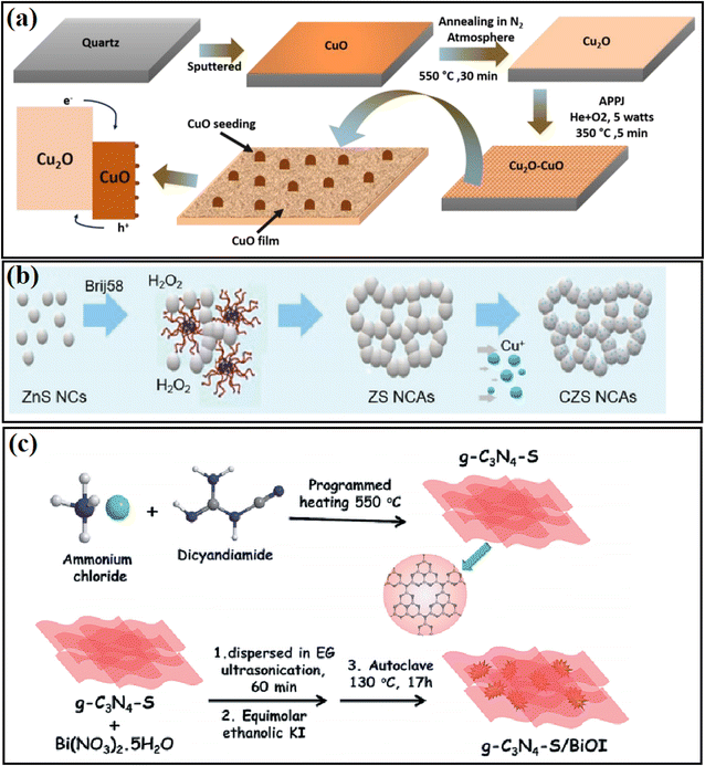 | ||
| Fig. 3 (a) Flowchart of the synthesis process for the Cu2O/CuO heterojunction electrode. Reproduced with permission from ref. 48. Copyright 2020, Elsevier. (b) Schematic representation of the synthesis of mesoporous ZnS (ZS) and Cu-doped ZnS (CZS) NC-linked assemblies (NCAs). Reproduced with permission from ref. 49. Copyright 2020, the Royal Society of Chemistry. (c) Synthetic strategy of g-C3N4-S/BiOI heterojunction composite using the in situ strategy. Reproduced with permission from ref. 50. Copyright 2019, the Royal Society of Chemistry. | ||
A similar design was also reported by Kang and coworkers,51 where they introduced a thin film of black TiO2 (BT) between TiO2 and Au cocatalyst by using an in situ electrochemical anodization approach (Fig. 4a). The existence of BT guaranteed the highly-uniformed deposition of the Au cocatalyst on the top of the mesoporous TiO2-BT nanotube array, resulting in a 10 times enhancement of the photocatalytic H2 evolution reactivity over conventional TiO2 nanotube (Fig. 4c and d). Compared with pure TiO2, the heterojunction formed by TiO2 and BT exhibited better photocatalytic ability because the TiO2-BT interface had a good conduction band arrangement, which makes the transfer of electrons from the conduction band of TiO2 to the conduction band of black TiO2 easier and promotes the separation of electron–holes pairs. Thus, the black TiO2 acts as a buffer layer for the TiO2 conduction band electrons in the TiO2-BT/Au system, which allows efficient photogenerated electrons to be transferred to Au nanoparticles, and then into the TiO2 pores that suitable for H2 generation (Fig. 4b).
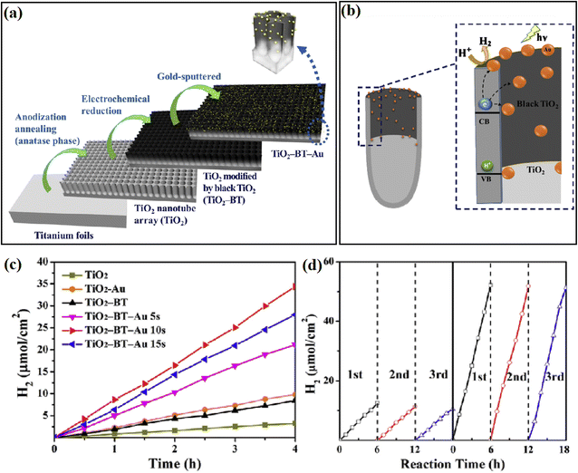 | ||
| Fig. 4 (a) Method for the synthesis of TiO2-BT-Au, (b) proposed mechanism of photocatalytic hydrogen evolution on TiO2-BT-Au 10s, (c) H2 evolution rates of different catalysts, and (d) cycle test of photocatalytic H2 evolution over TiO2 and TiO2-BT-Au 10s. Reproduced with permission from ref. 51. Copyright 2018, Elsevier. | ||
During the in situ growth method, passivation materials nucleate and grow spontaneously from the body phase of the substrate materials, thus having good interface compatibility with the substrate materials, which greatly reduces the defects and stresses caused by the direct contact of different semiconductors. However, this method also faces shortcomings, as follows: (1) in the in situ growth method, some critical properties, such as crystallinity, species and thickness of the passivation layer, are difficult to control, although some reports attempted to regulate the properties of the passivation layer through the in situ synthesis conditions. (2) Limited by the properties of the substrate materials and the crystal growth process, the type of passivation layer can hardly be regulated by the in situ growth method.
3.2 Deposition method
To precisely control the type and thickness of the passivation layer, deposition methods, including atomic layer deposition (ALD), electrochemical deposition, electron beam evaporation, have been adopted in the past few decades, in which researchers not only can choose different types of passivation materials according to the need, but also control their thickness and crystallinity through the deposition conditions.52–58 For example, Zhang et al.52 covered an Al/Al2O3 passivation layer on the surface of TiO2/Cu2O hybrid substrate by using magnetron sputtering method (Fig. 5a), where the thickness of the deposited Al layers could be regulated to 10, 20, and 30 nm. Furthermore, ALD is a widely accepted method for the deposition of an ultrathin passivation layer, in which the thickness of the deposition layer can be controlled at the atomic level due to its self-limited growth character.54–58 For example, the conformal growth of a 1 nm-thick TiO2 shell on ZnO NAs was realized using the ALD technique. Bai and coworkers55 deposited a TiO2 protection layer on the surface of a 3D Si nanowire trunk/ZnO nanowire branch (Fig. 5b) and found that a thin layer of TiO2 could efficiently protect the photocatalyst from corrosion. To accelerate the separation of electrons and holes by improving the interface properties, Feng et al.56 deposited a thin Al2O3 passivation layer between C QDs and TiO2 NRs using the ALD technique (Fig. 5c). The highest H2 evolution activity was obtained when the thickness of Al2O3 was 5 nm.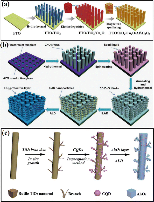 | ||
| Fig. 5 (a) Schematic diagram of the preparation process of the TiO2/Cu2O/Al/Al2O3 photoanode. Reproduced with permission from ref. 52. Copyright 2020, Science Press. (b) Schematic diagram of the processes for the fabrication of 3D ZnO NWA-CdS. Reproduced with permission from ref. 55. Copyright, 2016 Wiley. (c) Preparation of CQDs/3D-TiO2 NRs with a 5 nm Al2O3 layer. Reproduced with permission from ref. 56. Copyright 2018, The Royal Society of Chemistry. | ||
Also, our group57 controlled the deposition thickness of the Al2O3 interlayer by tuning the deposition cycle from 1 to 10 and found that 2 cycles of Al2O3 deposition resulted in 1.1 times higher H2 evolution ability than the sample without Al2O3 deposition. It was found that a too thin or too thick passivation layer was not conductive to the improvement in PHE activity. Usually, the transfer of charge carriers could be sped up through the tunneling effect when an interfacial passivation layer with a thickness of less than 2 nm was inserted,54 but the ultrathin layer may increase the possibility of generating weak points, thus losing the partial passivation effect.
Chen et al.58 discussed the influence of the fabrication method on the passivation effect of a TiO2 seed layer by fabricating the layer using the spin coating (SC), magnetron sputtering (MS) and ALD methods. It was found that the different fabrication methods resulted in different crystallinity in the TiO2 layer, which affected the band alignment between the semiconductors, and finally resulted in different PHE performances. Luo et al.59 introduced a TiO2 layer between FTO and Fe2O3 through the ALD method, where the deposited TiO2 served as a passivation layer and dopant source for the Fe2O3 photoanodes, which boosted their photocurrent by suppressing the substrate/hematite interfacial charge recombination and increasing the electrical conductivity by enabling the incorporation of Ti4+ (Fig. 6).
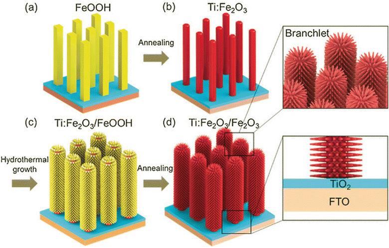 | ||
| Fig. 6 Synthesis of TiO2/Ti:Fe2O3 BNRs. Reproduced with permission from ref. 59. Copyright 2020, MDPI. | ||
To date, deposition methods have been adopted by many researchers to obtain a passivation layer. However, it should be noted that the passivation layers did not have the same effects in all cases, where the performance of the deposited passivation layers depends on many experimental variables, such as the deposition condition, the thickness and crystallinity of the deposition layer.
3.3 Chemical bonding modification method
In addition to the introduction of a coating layer, the construction of chemical bonding to release stress or regulate the charge distribution is also an emerging passivation method. Chemical bonding can be introduced in the host material by ion doping,60 plasma treatment,61 high-temperature heating,62–64 and solvent volatilization method.65 The application of these methods will be introduced in the next chapter.3.4 Other methods
Obviously, the realization of passivation engineering is not limited to the above-mentioned methods. In some reports, some special fabrication methods have also been adopted. For example, Liu et al.66 inserted an ultrathin Al2O3 passivation layer between TiO2 and NiOOH through a dipping method, followed by heating treatment (Fig. 7a). Kim67 decorated conformal titanyl phosphate with a thickness of ca. 5 nm on the surface of TiO2 using a sol–gel process. Liu et al.68 fabricated a grey rutile TiO2 passivation layer using a two-step calcination method. Nan et al.63 treated a CdS@ZnO heterostructure using a calcining technique, where the heating treatment was found to efficiently improve the interface connection and crystallinity of the semiconductors (Fig. 7b–e). At the same time, the injection of electrons from CdS to ZnO could be improved with an increase in the heating temperature (Fig. 7f). The further measurement found that a Cd0.8Zn0.2S buffer layer was formed between ZnO and CdS during the heating process, which efficiently released the interfacial stress, and thus paved a smooth pathway for the transfer of photogenerated charge carriers (Fig. 7g).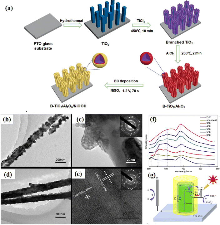 | ||
| Fig. 7 (a) Procedure for the synthesis of the B-TiO2/Al2O3/NiOOH photoanode, (b and c) TEM images of as-prepared and (d and e) calcined CdS/ZnO shell/core nanoarrays, (f) PL peaks of the CdS plane film and CdS/ZnO shell/core arrays calcined at different temperatures, and (g) schematic diagram of the PEC reaction mechanism on CdS/ZnO. Reproduced with permission from ref. 63. Copyright 2017, Elsevier. | ||
Table 1 lists most of the reported methods for the construction of a passivation layer with a comparison of their merits and shortcomings and their corresponding applicable systems.
| Fabrication method | Example | Advantage | Disadvantage | Applicable systems |
|---|---|---|---|---|
| In situ reaction method | Hydrothermal, solvothermal, wet-chemical sulfidation, photoreduction, hydrolysis, photo-deposition | Easy to operate, low cost | Difficult to accurately control the composition and content, limited passivation materials | Solid solution passivation layer, endogenous passivation layer, interfacial chemical bonding |
| Deposition method | Atomic layer deposition (ALD), chemical vapor deposition (CVD) | Controllable crystallinity, high purity and thinner layer | Time consuming, high cost | Exogenous passivation layer, interfacial layer |
| Chemical bonding modification method | Thermal polymerization, calcination | Easy to operate, low cost | Difficulty to accurately control, undefined mechanism | Ionic passivation layer |
| Electrochemical method | Electrostatic self-assemble, electrochemically anodization | Easy to operate, low cost, fine control to the passivation layer | Limited passivation materials | Exogenous passivation layer, interfacial layer |
| Other method | Plasma treatment, air oxidation, sol–gel | Easy to operate, low cost | Difficulty to accurately control | Exogenous passivation layer, surface layer |
4. Characterization of passivation engineering
The characterization of the passivation technique is an important task for evaluating its influence in photocatalysis. Also, to establish guidelines for passivation engineering in PHE, it is necessary to accurately identify the passivation action, control the passivation degree and correctly evaluate the passivation effect, and thus establish the structure–activity relationship between passivation action and catalyst performance. To date, various characterization methods have been reported for characterizing the passivation effect in photocatalytic systems. Herein, we classify the existing techniques into microscopic characterization and spectroscopic characterization.4.1 Microscopy characterization
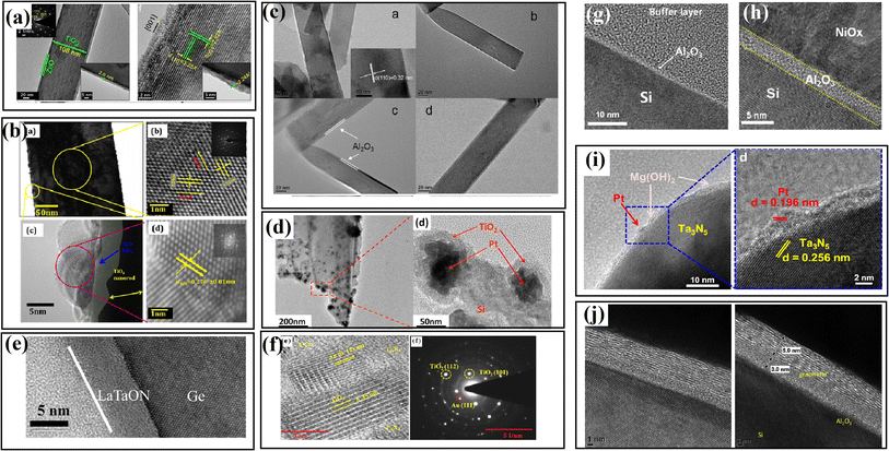 | ||
| Fig. 8 Some TEM and ACTEM images of the passivation-modified samples reported in the literature.68–76 (a) Reproduced with permission from ref. 68. Copyright 2016, Springer. (b) Reproduced with permission from ref. 69. Copyright 2015, the American Chemical Society. (c) Reproduced with permission from ref. 70. Copyright 2017, Bentham Science Publishers. (d) Reproduced with permission from ref. 71. Copyright 2015, the American Chemical Society. (e) Reproduced with permission from ref. 72. Copyright 2017, Elsevier. (f) Reproduced with permission from ref. 73, Copyright 2016 Elsevier. (g) and (h) Reproduced with permission from ref. 74. Copyright 2016, Elsevier. (i) Reproduced with permission from ref. 75. Copyright 2016, Academic Press Inc. (j) Reproduced with permission from ref. 76. Copyright 2018, Elsevier. | ||
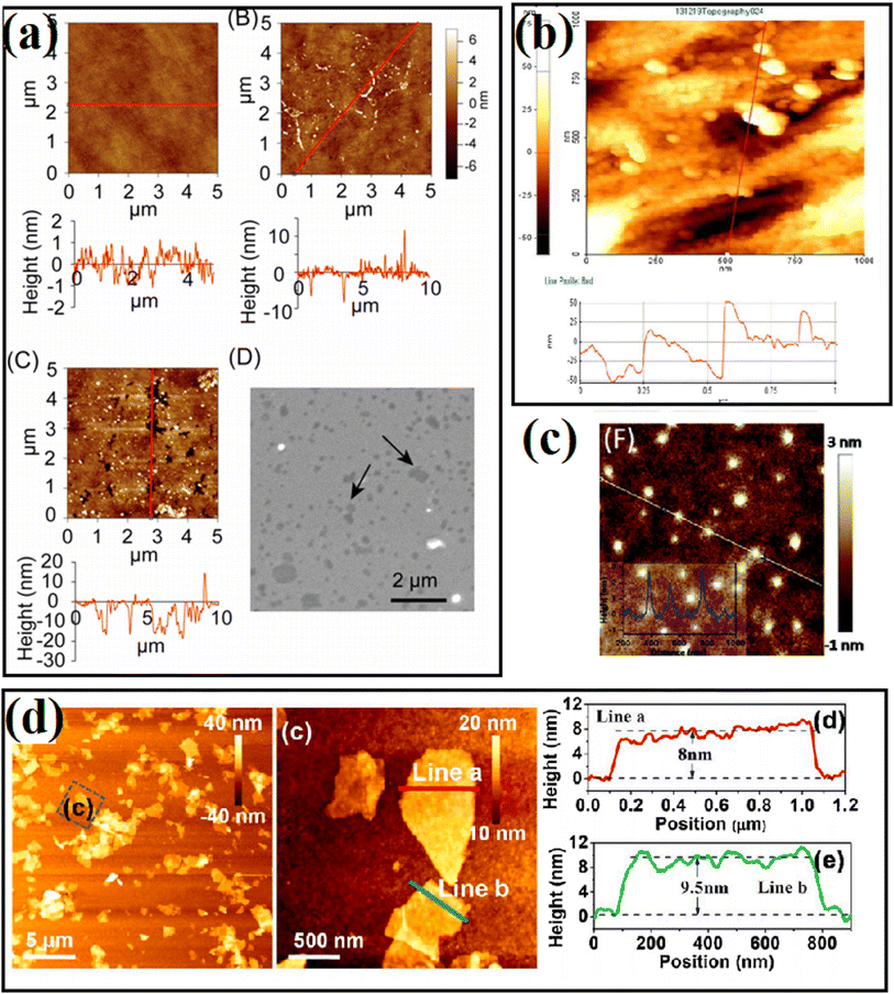 | ||
| Fig. 9 AFM images in passivation engineering.77–80 (a) Reproduced with permission from ref. 77. Copyright 2017, the American Chemical Society. (b) Reproduced with permission from ref. 78. Copyright 2019, Springer. (c) Reproduced with permission from ref. 79. Copyright 2020, MDPI. (d) Reproduced with permission from ref. 80. Copyright 2021, Elsevier. | ||
4.2 Spectral characterization
 | ||
| Fig. 10 EPR spectra of Fe@Ti-2 for (a) DMPO-˙O2−, (b) DMPO-˙OH and (c) TEMPO-h+. Reproduced with permission from ref. 84. Copyright 2022, Elsevier. | ||
Different from EPR, XPS can be widely applied for all types of inorganic and organic materials, as well as metals and semiconductors. The binding energy of different elements is closely related to the electron cloud density, thus reflecting the local change in chemical state and the interaction between different materials. In Yan's work,62 XPS spectra were measured to understand the effect of a carbon passivation layer on the interaction between SnO2 and g-C3N4. The binding energy of O–C in the pristine SnO2/g-C3N4 was lower than that in SnO2@C/CN-2, while the binding energy of π excitation in N 1s increased when a carbon layer was inserted in SnO2/g-C3N4, indicating that the strong interaction among carbon, SnO2 and g-C3N4 efficiently changed the electron density of the C and N atoms. Zhang et al.61 carried out XPS measurement to evaluate the effect of N treatment on the carrier accumulation capability of the MoS2/GaN heterostructure. As shown in Fig. 11a, before N treatment, the energy difference between Mo 3d5/2 and Ga 2p3/2 was 887.83 eV, while it increased to 888.36 eV after the N treatment, with a significant red-shift in the binding energy of Mo 3d5/2 towards a lower binding energy, indicating the enhanced accumulation of electrons on the surface of GaN. Xiao and coworkers65 found that the surface deposition of K+ resulted in an increased binding energy value of Ti 2p in KHB-TiO2, and thus confirmed that K+ can reduce the electron cloud density around Ti3+ and heal the defects in TiO2 through the passivation effect (Fig. 11b). By using XPS measurement, Kim67 observed the formation of a Ti–O–P bond and a slightly shifted XPS signal in H3PO4-passivated TiO2 (Fig. 11c), indicating the strong interaction between TiO2 and H3PO4.
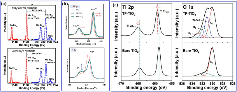 | ||
| Fig. 11 (a) Ga 2p and Mo 3d core-level spectra obtained from the MoS2/GaN interface without and with nitridation treatment. Reproduced with permission from ref. 61. Copyright 2018, the American Chemical Society. (b) Ti 2p and O 1s XPS spectra of TiO2, HB-TiO2 and KHB-TiO2. Reproduced with permission from ref. 65. Copyright 2023, Elsevier. (c) Ti 2p and O 1s XPS spectra of bare TiO2 and TP-TiO2. Reproduced with permission from ref. 67. Copyright 2018, MDPI. | ||
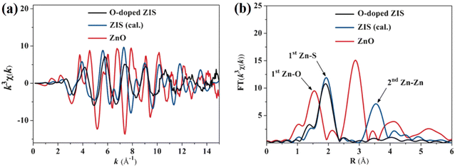 | ||
| Fig. 12 (a) Zn K-edge extended EXAFS oscillation function and (b) corresponding Fourier transforms of the O-doped ZIS nanosheets, calculated ZIS and ZnO. Reproduced with permission from ref. 85. Copyright 2016, Wiley-VCH. | ||
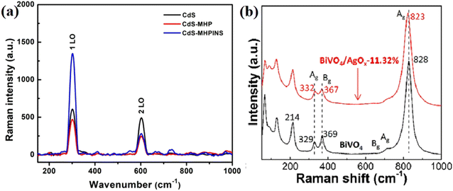 | ||
| Fig. 13 (a) Raman spectra of the pristine CdS nanowire and heterojunctions of CdS with C3N5 nanosheets. Reproduced with permission from ref. 89. Copyright 2021, the American Chemical Society. (b) Raman spectra of bare BiVO4 and BiVO4/AgOx-11.32% sample. Reproduced with permission from ref. 42. Copyright 2021, Elsevier. | ||
Nayak et al.78 fabricated an NiFe-LDH/N-GO/g-C3N4 nanocomposite using N-doped rGO as a passivation layer. In the PL spectrum, the introduction of N-rGO efficiently decreased the emission caused by the recombination of photogenerated charge carriers, indicating the suppressed charge recombination. In addition, two obvious PL peaks corresponding to the defect region and oxygen vacancies could be seen with different emission intensities with a changed in the amount of introduced passivation layer, indicating the importance of an appropriate passivation layer in manipulating the amount of defects and vacancies. Neuderth and coworkers90 studied the effect of a passivation layer on InGaN by using PL spectroscopy, as shown in Fig. 14b–d. The deposition of Al2O3 resulted in a significant increase in the PL intensity of the substrate, while a decrease in the PL intensity was obtained in the TiO2 deposited sample. By contrast, CeO2 barely displayed an effect on the PL of the substrate. This work demonstrated that PL spectroscopy is a direct tool reflecting the interaction between the passivation layer and the substrate.
 | ||
| Fig. 14 (a) PL spectra of NiFe LDH, CN, CNLDH and CNNGxLDH measured at the excitation energy of 380 nm. Reproduced with permission from ref. 78. Copyright 2019, Nature. (b) PL spectra of TiO2-, CeO2- and Al2O3-coated InGaN nanowires. Reproduced with permission from ref. 90. Copyright 2018, The Royal Society of Chemistry. | ||
In passivation engineering, spectroscopic techniques are mainly utilized for the qualitative analysis of defects or vacancies in the substrate materials. However, in actual research, different characterization methods are usually combined, and the different data support and assist each other, verifying the realization of passivation engineering from different perspectives and dimensions and revealing the impacts of passivation engineering on catalytic systems.
5. The categories and mechanism of passivation engineering in PHE
As mentioned, passivation engineering not only provides protection for the sensitive photocatalytic surface, but also inhibits the harmful inner charge recombination. As shown in Tables 2 and 3, passivation engineering can be divided into surface passivation and interfacial passivation according to the modification position. Based on our research, it was found that various materials, including metallic compounds, amorphous compounds, halogen, carbon, and graphene, have been utilized as a passivation layer, and different passivation mechanisms have been proposed by researchers in these systems. In the following paragraphs, we introduce the design and mechanism of these materials in passivation engineering in detail.| Catalyst | Passivation material | Fabrication | Type | Mechanism | Ref. |
|---|---|---|---|---|---|
| ZnO/MnO2/TiO2 | TiO2 | ALD | SP | Protecting substrate from photo-corrosion | 91 |
| Pt/TiO2/InAs/p-Si | TiO2 | ALD | SP | Protecting the vulnerable InAs | 33 |
| SiP/TiO2/Al2O3 | Al2O3 | ALD | SP | Providing fixed charge to promote the separation and transport of electrons and holes | 96 |
| TiO2-CdTe/Fe2O3 | TiO2 | Calcination | SP | Addressing the excessive surface defects and the slow carrier transfer | 114 |
| TiO2/Cu2O/Al/Al2O3 | Al2O3 | Air oxidation | SP | Protecting vulnerable substrate | 52 |
| BiVO4/AgOx | AgOx | Calcination | SP | Quenching the photogenerated holes to stabilize BiVO4 | 42 |
| VO-B/N-ZGO | B and N doping | Calcination | SP | Proving efficient charge compensation by B–N bond formation | 115 |
| C-Cu-CdS | Carbon | Solvothermal | SP | Protecting vulnerable substrate | 116 |
| Al2O3-CQDs/TiO2 | Al2O3 | ALD | SP | Restraining electrons from being captured by surface trap states through fixed negative charge | 56 |
| TiO2/Ti/Si | TiO2 | Sputtering | SP | Protecting Si from surface passivation | 53 |
| CdSe/CdS | CdS | Oil bath | SP | Decreasing the surface-deep trap states of CdSe, inducing tunnel effect | 101 |
| C@SiNW/TiO2 | Carbon | Calcination | SP | Protecting the Si from oxidation | 34 |
| Cu-TiO2@C | Carbon | Thermal reduction | SP | Providing a chemical protection to the coated Cu nanoparticle | 95 |
| KHB-TiO2 | K+ | Calcination | SP | Healing the electronic structure of the TiO2 surface | 65 |
| TiO2@Si | TiO2 | ALD | SP | Protecting silicon from photo-oxidation | 117 |
| Fe2O3@Fe0@black-TiO2 | Fe2O3 | Air oxidation | SP | Protecting Fe0 from oxidation | 118 |
| CdSe-Cl | Cl | Water bath | SP | Decreasing electron trap states on the surface of CdSe | 103 |
| TiO2/conformal titanyl phosphate | Conformal titanyl phosphate | Sol–gel | SP | Promoting the production and stabilization of hydroxyl radicals on the surface of TiO2 | 67 |
| CoS2-Si | CoS2 | Photolithography and dry etching | SP | Preventing Si from oxidation | 94 |
| CdSe/CdS/Pt | CdS | Hydrothermal | SP | Eliminating surface traps | 93 |
| InxGa1−xN/GaN/ultra-thin oxides | TiO2, CeO2 and Al2O3 | ALD | SP | Eliminating surface states | 90 |
| Zn1−xCdxS/NiO | NiO | Photodeposition | SP | Inhibiting substrate from photocorrosion | 119 |
| Cu-doped AgIn5S8/ZnS | ZnS | Solvothermal | SP | Passivating surface defects and enhancing photogenerated charge transportation | 120 |
| Cu2ZnSnS4/CdS/TiO2 | TiO2 | Hydrolysis | SP | Inhibiting substrate from photocorrosion | 98 |
| SnO2@C/CN | Carbon | Calcination | IP | Stabilizing small size semiconductors; inducing the formation of strong internal electric field | 62 |
| CdS/CdZnS/ZnO | CdZnS | Calcination | IP | Decreasing the interface stress by minimizing lattice mismatch | 63 |
| TiO2-BT-Au | Black TiO2 | Electrochemical anodization | IP | Electronic storage and prevention of hole recombination | 51 |
| NiFe-LDH/N-rGO/g-C3N4 | N-rGO | Electrostatic self-assembly | IP | Providing bridge for the combination of different 2D nanolayers, enhancing interfacial charge interactions | 78 |
| CdS@Al2O3@CdS | Al2O3 | ALD | IP | Decreasing interfacing stress and facilitating charge transfer through fixed negative charge | 57 |
| Cu/Cu2S/ZnS | Cu2S | Wet-chemical sulfidation | IP | Increasing interfacial charge transfer and changing the Helmholtz layer potential drop | 49 |
| CoNi-C3N4/CdS | Co–S bonding | Photoreduction method | IP | Accelerating electron transfer through Co–S bonds | 32 |
| P-C3N4/Ni | P–Ni bonding | Thermal polymerization | IP | Bridging incompatible C3N4 and Ni through N–P–Ni bonding | 60 |
| B-TiO2/Al2O3/NiOOH | Al2O3 | ALD | IP | Reducing the surface defects of TiO2 and benefiting the extraction of holes to the surface | 66 |
| MoS2/GaN | N2 | Plasma treatment | IP | Facilitating electron accumulation capability through N2-induced conduction band offset | 61 |
| g-C3N4/GO/BiOI | GO | Oil bath | IP | Forming close energy band to enhance electron transfer from g-C3N4 to BiOI | 107 |
| Passivation mode | Materials | Mechanism | |
|---|---|---|---|
| Surface passivation | Metallic compound | SiO2, Al2O3 | Providing the substrate from photo-corrosion |
| TiO2 | Improving the surface charge separation | ||
| Ti3(PO4)4, CdS, CoS2 | Reducing surface defect states through the formation of chemical bonding | ||
| ZnO, CeO2 | Reducing the tunneling barrier and interfacial resistance | ||
| Al2O3, MnO2, Cr2O3, TiO2 | Inhibiting the photocatalytic active materials from inactivating oxidation | ||
| Ionic passivation layer | K+, Cl−, other halogen ions | Healing surface defect and balancing the density of free electrons | |
| Interfacial passivation | Amorphous compounds | Al2O3, TiO2 | Releasing interface stress, increasing charge tunneling ability |
| GO, rGO | Decreasing the band barrier and interface resistance between the directly contacted semiconductors | ||
| Carbon | Stabilizing small size semiconductors; inducing the formation of strong internal electric field | ||
| Solid solution | Sx–In–P1−x, CdZnS | Decreasing the interface stress by minimizing lattice mismatch | |
| Interfacial chemical bonding | Ni–P–N, Co–S bonds | Bridging incompatible semiconductors; forming atomic level electron transfer channel | |
| Impurity atoms | N, Nd, C | Manipulating the energy band structure, increasing charge carriers generation speed and decreasing recombination losses | |
5.1 Surface passivation
The surface of a catalyst is the most active position because of the accumulation of photogenerated electrons and holes, where the photogenerated electrons are consumed by protons (H+) to generate hydrogen or consumed by a more competitive reductant, and the photogenerated holes easily trigger the oxidation reaction of the catalyst itself, thus resulting the deactivation of the catalyst. For example, the surface sulfide ions (S2−) in metal sulfide-based photocatalysts are easily oxidized by photogenerated holes to form sulfate (SO42−) and/or sulfur (S0), resulting in their deactivation, and the Ag+ in silver-containing compounds can be reduced to Ag0 by photogenerated electrons, leading to the decomposition of the compounds.90,91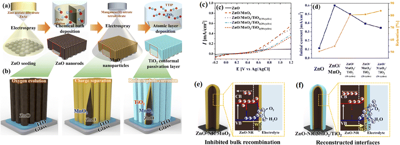 | ||
| Fig. 15 (a) Schematic of the fabrication of ZnO/MnO2/TiO2 nanorods, (b) illustration of the effect of each coated layer, (c) and (d) are respectively photocurrent density and stability of the samples, and effects of (e) MnO2 in promoting charge separation and (f) TiO2 as a passivation layer. Reproduced with permission from ref. 91. Copyright 2020, Elsevier. | ||
Rasamani et al.92 passivated Pt-tipped CdSe nanorods using an epitaxially grown atomic-level CdS layer to efficiently eliminate the surface defects/trap states in the CdSe nanorods. It was found that after the treatment, the sample displayed 6.5 times higher H2 evolution ability. Besides, the formation of strong chemical boding on the surface of bare catalysts has also been proven to be an efficient way to decrease the adverse surface charge recombination by eliminating the surface states. In 2015, Kim67 modified TiO2 photocatalysts with a titanyl phosphate passivation layer, where the phosphate anions were strongly bound on the surface Ti atoms with oxygen bridges, inducing the formation of Ti–O–P–O bonds, which resulted in a reduction in the trap states originating from the Ti3+ defects. The decoration of the passivation layer enabled a long-term photochemical performance with the enhanced photocatalytic activities of TiO2. Chen et al.93 deposited an integrated cobalt disulfide passivation layer on Si microwires, where the covering CoS2 layer resulted in the formation of a fluffy surface (Fig. 16a–d) and dramatically improved the photocatalytic stability and activity of Si (Fig. 16e and f). It was found that the CoS2-Si hybrids displayed lower charge transfer resistance among the photo-absorber, co-catalyst, and redox couples due to the decoration of CoS2 (Fig. 16g–i). At the same time, the XANES spectra revealed that more vacancies were present in the unoccupied S-3p states of the CoS2-Si-250 electrode, which indicated that the CoS2-Si electrode presented a lower negative charge of S22− and formed a weaker S–Hads bond strength to promote the water splitting efficiency. Furthermore, the deposited CoS2 layer protected Si from directly exposure in liquid, and thus working worked as a passivation layer to defend Si from oxidation, which efficiently improved the stability of the sample.
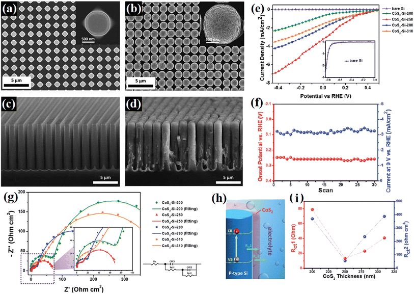 | ||
| Fig. 16 (a and b) Top view and (c and d) cross-sectional SEM images of bare Si and CoS2-Si-250 microwire arrays. (e) Linear-sweep voltammograms of CoS2-Si electrodes with various CoS2 thicknesses, (f) onset potential and photocurrent of the CoS2-Si electrode versus the number of scans, and (g) electrochemical impedance spectra of CoS2-Si electrodes at 0.4 V bias under solar illumination. (h) Schematic illustration of charge transfer resistance between the composition materials of the photoelectrode (Rct1) and between the photoelectrode and redox couples in the electrolyte (Rct2). (i) Charge transfer resistance versus CoS2 thickness of CoS2-Si electrodes. Reproduced with permission from ref. 93. Copyright 2015, the Royal Society of Chemistry. | ||
Another widely utilized strategy is protecting the vulnerable surface by using a stable chemical layer, such as Al2O3 and TiO2. Feng et al.56 anchored an Al2O3 ultra-thin layer on the surface of CQDs/TiO2 using the atomic layer deposition method, and it was found that the introduction of Al2O3 significantly improved the IPCE value and photoconversion efficiency of the sample (Fig. 17). However, a crucial factor that needs to be considered is the thickness of the passivation layer. A too thick passivation layer may result in a decline in photocatalytic performance due to the quickly developed adverse factors, resulting in the loss of light harvest ability, charge transfer ability, and the limited exposure of active sites. In this study, it was found that the sample behavior was obvious correlated with the thickness of the deposited Al2O3 layer. Consequently, it was found that 5 nm is the best parameter for Al2O3 coating. Alternatively, a too thin coating layer could not passivate the trapping state effectively. Further, a too thick coating prevented the photogenerated electrons and holes from migrating to the surface of the nanorods by transiting the Al2O3 layer due to its large band gap. The effect of the Al2O3 layer in the system is shown in Fig. 17d, where negative charges exist between the Al2O3 layer coated using the ALD technique and the photocatalyst surface. The surface band bending induced by the electron depletion on the surface of the photocatalyst restrains the photogenerated electrons from being captured by the surface trap states, and thus isolates the photoinduced charges in space, reduces their recombination rate and suppresses the back reaction effectively.
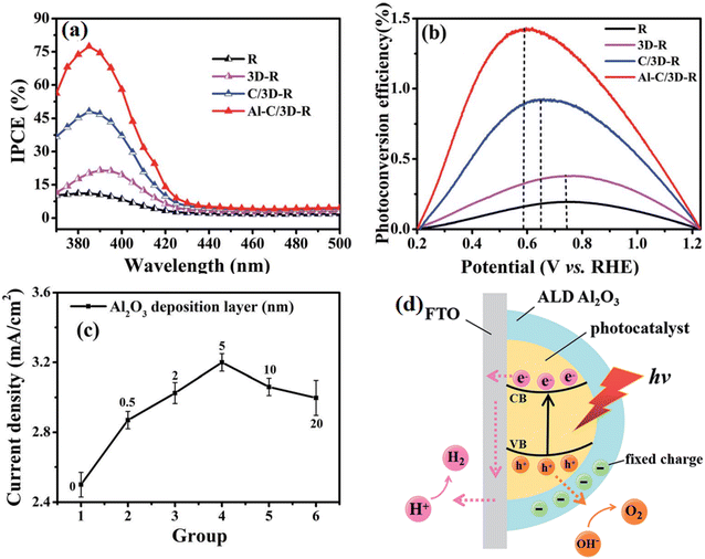 | ||
| Fig. 17 (a) IPCE spectra and (b) calculated solar-to-hydrogen (STH) efficiencies of the samples. (c) Line chart measured at 1.23 V vs. RHE of thickness of Al2O3 layer. (d) Mechanism model for the role of Al2O3 coating in the separation of electron–hole pairs. Reproduced with permission from ref. 56. Copyright 2018, the Royal Society of Chemistry. | ||
In addition to photo-corrosion, another factor playing a role in the deactivation of catalysts is self-passivation, which means that some active components in the catalyst are converted into new substances that do not have catalytic activity during the catalytic reaction. For example, Si has one of the best band gaps and band alignments as the photocathode of a two-photo-absorber water-splitting device, but one of the major limitations of silicon is that it is easily oxidized to SiO2, which does not have catalytic activity. Also, Cu photocatalysts can only be kept in an oxygen-free environment because Cu nanoparticles are easy oxidized by oxygen, which limits the applications and studies using Cu catalysts. An exciting idea is that the surface passivation strategy can be utilized to inhibit the passivation of some active components themselves to extend the lifetime of catalysts. The typical cover layers reported include Al2O3, MnO2, Cr2O3, and TiO2.87,88,91–96 For example, Seger et al.53 deposited a sputtered 100 nm TiO2 layer on top of a thin Ti metal layer, which was found to be efficient in protecting the Si photocathode from oxidation during photocatalytic H2 evolution. Chen and coworkers94 covered a Cu-TiO2 nanocomposite using a carbon protection layer without changing the basic morphology and structure of the substrate catalyst. Cu-TiO2@C could effectively adsorb hydroxyl radicals, improving the electron transfer speed between TiO2 and Cu nanoparticles, thereby greatly improving the photocatalytic activity of TiO2 (Fig. 18). In addition, the carbon layer could provide a chemical protection to the Cu nanoparticles and increase the stability of the photocatalysts.
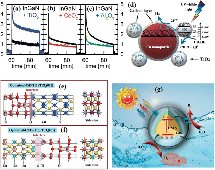 | ||
| Fig. 18 (a–c) Influence of different ALD coatings on the PC of InGaN/GaN NWs: PC measurements of TiO2-, CeO2- and Al2O3-coated NWs. Reproduced with permission from ref. 90. Copyright 2018, Elsevier. (d) Influence of different ALD coatings on the PC of InGaN/GaN NWs: PC measurements of TiO2-, CeO2- and Al2O3-coated NWs. Reproduced with permission from ref. 94. Copyright 2019, Elsevier. (e) and (f) Optimized interfaces of CdS(111)-TiO2(001) and CZTS(001)-TiO2(001), respectively. (g) Mechanism of overall water splitting over the CZTS/CdS/TiO2/Pt double-heterojunction photocatalyst with PFDL assistance under visible illumination. Reproduced with permission from ref. 94. Copyright 2022, Elsevier. | ||
Besides, Al2O3 was also utilized as a cover layer to passivate the inner catalyst from rapid charge recombination due to its special fixed negative charge. By using the ALD method, Zhang et al.95 deposited Al2O3 on the surface of an SiP QDs/TiO2 NR heterostructure and obtained significantly enhanced hydrogen evolution ability over the catalyst. As shown in Fig. 19a, a TiO2 nanorod (NRs) array was firstly grown on FTO glass through the hydrothermal method, and subsequently they deposited SiP quantum dots (QDs) on the TiO2 NR array to form SP QD/TNR composites using a continuous dip coating approach. Subsequently, a thin Al2O3 layer was coated on the surface using the ALD method. The morphology and element distribution of the sample can be observed on right of Fig. 19a. The experimental results indicated that the introduction of an Al2O3 layer obviously improved the photoconversion efficiency of the sample (Fig. 19b and c). In addition, it was found that the photoelectric behavior of the sample varied with the thickness of the Al2O3 layer, an Al2O3 layer with a thickness of about 3 nm resulted in the highest current density (Fig. 19d and e). When the thickness of Al2O3 was less than 3 nm, the Al2O3 layer was too thin to effectively passivate the surface state of SiP/TiO2 and prevent photo-corrosion, whereas a too thick Al2O3 layer prevented the absorption of light and the transmission of photogenerated charge carriers to the surface of the catalyst due to its large bandgap, as shown in Fig. 19f.
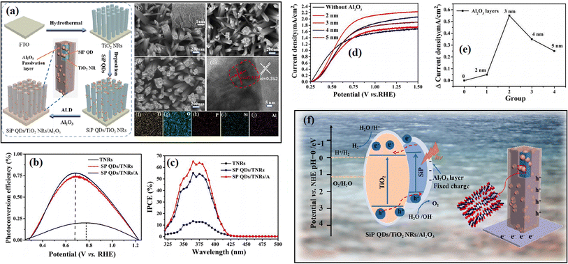 | ||
| Fig. 19 (a) Schematic of the synthesis of SiP QDs/TiO2 NRs/Al2O3 and the morphology of the sample. (b) Calculated solar-to-hydrogen (STH) efficiencies and (c) IPCE spectra of the samples. (d) LSV curves and (e) corresponding line charts measured at 1.23 V vs. RHE of SiP QDs/TiO2 NRs/Al2O3 with different dipping times in SiP QD solution. (f) Schematic of the nanostructure and charge separation and transfer mechanism of the sample. Reproduced with permission from ref. 95. Copyright 2022, Elsevier. | ||
Surface passivation is the external manifestation of multiple complex effects in the cover layer. Qiu et al.96 studied the effect of a surface TiO2 passivation layer on the PHE ability of GaAs, and found that the TiO2 layer hosted active surface states on GaAs, which increased the recombination rate of photogenerated electron–hole pairs. At the same time, the introduced TiO2 layer dramatically decreased the potential barrier for photocatalytic reactions, and this benefit outweighed the unfavorable effects of charge recombination and resulted in an enhancement in the photocurrent density. In addition, they demonstrated that the thickness of the TiO2 layer also has an obvious effect on the sample. The highest PHE efficiency was obtained with the loading of a 1 nm TiO2 passivation layer, while no improvement was observed in the 10 nm TiO2-decorated sample, which is because the insulating nature of TiO2 eventually outweighed its benefits. Neuderth et al.90 studied the surface passivation effect of ultra-thin TiO2, CeO2 and Al2O3 coatings on the photoelectrochemical performance of InxGa1−xN/GaN nanowires, and found that the best passivation of surface states resulted in an increase in the anodic photocurrent by a factor of 2.5 with the deposition of 5 nm TiO2. By contrast, the covering of CeO2 and Al2O3 resulted in a decrease in the photocurrent (Fig. 18a–c), which is because the high band energy offset of Al2O3 to InGaN suppressed the transfer of photocarriers and resulted in enhanced radiative recombination, while the increased defect recombination brought by CeO2 aggravated the carrier losses. Zhang et al.97 investigated the role of TiO2 on the surface of Cu2ZnSnS4/CdS hybrids. Based on theoretical calculation, they claimed that the formation of Cd–O and Ti–S covalent bonds between TiO2 and CdS is crucial in achieving a well-matched interface architecture between the photocatalyst and the chemically inert TiO2 protective layer (Fig. 18e–g), which restrained the photo-corrosion of the catalyst induced by the formed nascent O2 and remarkably enhanced the catalyst stability during photocatalytic water splitting. Yu et al.98 studied the origin of enhanced PHE activity in g-C3N4/TiO2 through DFT calculations, and they claimed that the different modifications on TiO2 surface will greatly affect the distribution of electrons and holes at the heterojunction interface, where oxygen vacancy and hydrogen passivation showed a more significant influence on the g-C3N4/A001 interface and induced more significant charge separation.
By using Au-tipped CdS nanorods as a model, Ben-Shahar et al.99 studied the effects of different surface passivation layers on the photocatalytic function of hybrid nanoparticles. They found that the surface coating affected the trapping of photogenerated charge carriers at the surface defects, thus changing the photocatalytic efficiency. The apparent quantum yield (AQY) of the photocatalysts strongly depended on the surface passivation layer, where the lowest AQY was observed for thiolated alkyl ligands, while the best photocatalytic activity was found for the PEI-coated sample (Fig. 20a). The corresponding measurements indicate that the improved H2 evolution activity is correlated with the effect of passivation of the surface traps. As shown in Fig. 20b and c, a faster bleach recovery was observed for the PEI-coated hybrid nanoparticles, which means faster and more efficient charge separation. This work demonstrated that different coatings affect the surface passivation efficiency in trapping the charge carriers.
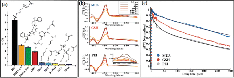 | ||
| Fig. 20 (a) Apparent photocatalysis % QY values for a wide range of surface coatings, including thiolated alkyl ligands, GSH, and polymer coating. (b) Transient absorption spectra of CdS-Au HNPs for different surface coatings at 450 nm excitation. Expansion of the Au plasmon region for the PEI coating are presented in the inset (lower left frame). (c) Normalized transient absorption kinetics of the bleach recovery at 460 nm, corresponding to the first exciton transition of the CdS nanorod component, together with the exponential fits (continuous lines) for CdS-Au HNPs with different surface coatings. Reproduced with permission from ref. 99. Copyright 2015, Wiley. | ||
Besides, the harmful trap states created by the intrinsic defects in some semiconductors can also be passivated by covering a protection layer.100 In 2011, Thibert and co-workers101 found that the coverage of a CdS shell efficiently enhanced the H2 evolution ability of CdSe quantum dots (DSs), while CdSe itself was completely inactive in pure water (Fig. 21a). Broad-band transient absorption spectroscopy was performed to reveal the defect states in the catalyst. As shown in Fig. 21b, an obvious emission peak arose from the recombination of deeply trapped charge carriers at 700 nm in CdSe QDs but absent in CdSe/CdS, indicating that the CdS shell passivated the deep traps caused by the defects in CdSe. Based on the broad-band transient absorption spectroscopy measurements, the authors proposed that the surface-deep trap states with energies lying below the reduction potential necessary for H2O reduction were passivated by the CdS shell, thus efficiently facilitating the utilization of photogenerated charge carriers and boosting the H2 generation (Fig. 21c and d). In addition, Tongying et al.102 investigated the lifetime of photogenerated charge carriers in CdS and the CdSe/CdS system by using femtosecond transient differential absorption (TDA) spectroscopy, and found that the coverage of CdS efficiently prolonged the lifetime of electrons and suppressed the harmful recombination caused by trap states. Moreover, the CdS shell provided electrons to the CdSe core and formed a type I energy transfer mechanism. The combination of defect passivation and the supplementary of additional carriers from the CdS shell significantly improved the H2 generation rate of bare CdSe.
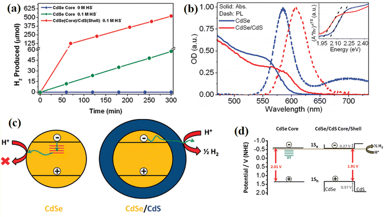 | ||
| Fig. 21 (a) Photocatalytic hydrogen evolution for CdSe and CdSe/CdS QDs in pure H2O and 0.1 M HS solution under visible light illumination from a 300 W Xe lamp equipped with a 400 nm long pass filter. (b) Static absorption (solid lines) and photoluminescence (dashed lines) spectra of CdSe (blue lines) and CdSe/CdS core/shell QDs (red lines). (c) and (d) Mechanisms of CdS in passivating the trap states of CdSe and facilitating H2 evolution. Reproduced with permission from ref. 101. Copyright 2011, the American Chemical Society. | ||
Inhibiting the easily inactivated photocatalyst surface by using a chemical inert covering layer is efficient in prolonging the working lifetime of photocatalysts, but this process is often at the cost of reducing their catalytic activity. Thus, to minimize the adverse influence of the coating layer on the catalytic activity, some key points should be considered in the selection and design of the coating layer, as follows: (1) the covering layer should have good electrical conductivity or proper thickness to minimize its effect on the migration of photogenerated charge carriers. (2) The introduction of a coating layer should not affect the light absorption performance of the substrate catalyst. (3) The coating layer should have good interfacial compatibility or the ability to form chemical bonds with the substrate catalyst, thus avoiding the generation of new defects. (4) Suitable energy band arrangement is also an important factor to minimize the loss of catalytic activity.
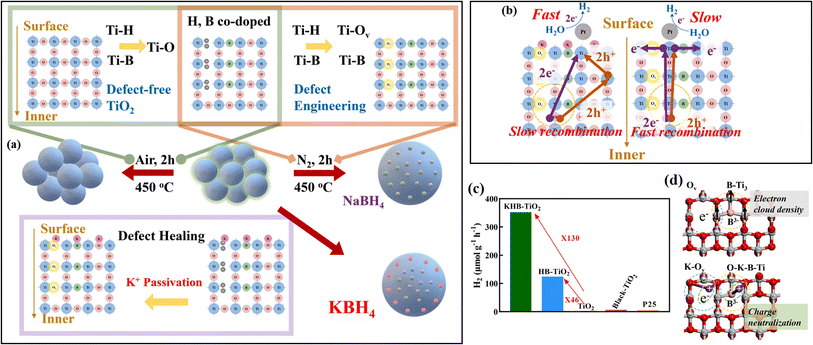 | ||
| Fig. 22 (a) Strategies for the synthesis of TiO2, HB-TiO2, and KHB-TiO2. (b) Photoelectron migration mechanism of KHB-TiO2 and HB-TiO2. (c) Hydrogen production efficiencies of different samples in 1 h. (d) Mechanism of K+ healing the electronic structure of TiO2 surface. Reproduced with permission from ref. 65. Copyright 2021, the American Chemical Society. | ||
At the same time, Kim et al.103 investigated the H2 evolution ability of chlorine-passivated CdSe nanocrystals, and found that Cl passivation removed the electron trap states in the CdSe NCs and resulted in an increase in the photoluminescence quantum yield from 9% to 22% after Cl treatment. This is because the introduced ammonium chloride solution resulted in Cl-passivation of the surface dangling bonds, and thus inhibited the harmful consumption of electrons from the surface of CdSe (Fig. 23a and b). Moreover, by controlling the size of CdSe, they found that the photocatalysis was enhanced significantly in 4.5 nm CdSe NCs after the Cl treatment, whereas smaller CdSe NCs exhibited lower photocatalytic activity after Cl treatment. The different changing trends indicate that the Cl atoms passivate the surface trap states without altering the density of native organic ligands because both the conduction band edge and trap states in the small-size CdSe are above the water reduction potential (Fig. 23c and d).
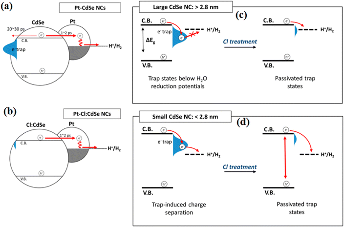 | ||
| Fig. 23 Electron dynamics in (a) Pt-CdSe and (b) Pt–Cl:CdSe NCs. (c) and (d) Illustration of the effect of Cl on surface traps at different NC size ranges during photocatalytic hydrogen generation. Reproduced with permission from ref. 103. Copyright 2016, the American Chemical Society. | ||
Liu et al.104 investigated the halogen edge passivation effect of antimonene nanoribbons on the H2 evolution reaction with first-principles density functional theory calculations. It was found that both the armchair and zigzag structures of the antimonene nanoribbons can be relaxed to a more stable state by the halogen atom than the hydrogen atom-passivated ones due to the larger electronegativity and mass of the halogen atoms. In addition, it was also noticed that the passivation effect caused by the halogen endowed the catalysts with different band gaps. As a result, the tensile strain can promote the solar to hydrogen transfer efficiency. All the samples satisfied the REDOX potentials for H2 evolution under tensile strain of greater than 4%, while the maximum value can reach the theoretical limit of 17.51% under the tensile strain of 12%.
Some self-modification strategies can also create an inert protection layer on unstable substrates. For example, Liu et al.59 treated rutile TiO2 using a two-step calcination method. A dense layer with a thickness of 2–5 nm was formed on the outermost layer of the rutile TiO2, resulting in a change in color from white to gray (Fig. 24a and b). The EPR measurement reflected that a large amount of O vacancies were formed during the high-temperature treatment, which can improve the photogenerated carrier separation and transmission efficiency (Fig. 24c). The formed dense surface passivation layer efficiently hindered the further diffusion and infiltration of oxygen molecules into the interior oxygen vacancies, thus endowing the photocatalyst with an outstanding long-time reaction stability.
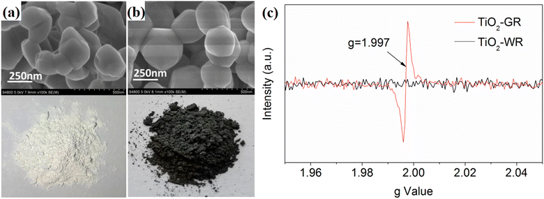 | ||
| Fig. 24 (a and b) Morphology of TiO2-gray rutile (TiO2-GR) and TiO2-white rutile (TiO2-WR). (c) EPR spectra of TiO2-GR and TiO2-WR. Reproduced with permission from ref. 59. Copyright 2020, MDPI. | ||
In total, the surface of photocatalysts can be passivated by using some ions or passivation layers, where the surface passivation of photocatalysts is essential not only for increasing their efficiency, but also for enhancing their resistance to corrosion and dissociation, which are caused by photogenerated intermediates.
5.2 Interfacial passivation
With the development of technology for the preparation and characterization of nanomaterials, the construction of heterostructure systems has been considered more promising in obtaining much improved H2 evolution ability due to the formation of an inner electric field on the interface, which is effective in reducing the recombination of photogenerated electrons and holes. However, an inescapable fact is that the high separation of charge carriers at interface requires intimate contact and low mismatched interface between two semiconductors, which is difficult to precisely achieve because the difference in lattice parameters and crystal growth directions between semiconductors often causes serious distortion and mismatch at the interface. Lattice distortion at the interface creates a high density of defect states at the interface, where the formed defects act as trapping sites for charge carriers and result in decreased photocatalytic ability.105,106 In the long term, the performance of photocatalytic systems was found to be much lower than expected, and one of the main factors for this is the harmful charge recombination caused by doping, vacancy, plastic deformation, and interface lattice mismatch. To date, these shortcomings have seriously limited the design and fabrication of high-performance heterostructure photocatalysts. Thus, by using an interfacial passivation strategy, the above-mentioned long-term issue in heterostructures is expected to be resolved, significantly improving the separation efficiency of charge carriers.In general, to passivate interfacial defects, some materials with an amorphous structure or good interface compatibility are introduced, where the core aim is to release the interfacial stress between semiconductors. At the same time, the interfacial passivation layers act as a tunneling barrier to inhibit the interfacial charge carrier recombination and passivate the surface states, which can reduce the non-radiative carrier recombination. In addition, some passivation materials are equipped with a special charge effect, which usually results in improved charge transport in the host semiconductors.
To gain an in-depth understanding of the role of the interfacial passivation layer in hybrid systems, our group57 fabricated a CdS@Al2O3@ZnO photocatalyst by introducing atomic-level ultrathin Al2O3 between CdS and ZnO through the ALD method, where an intimately contacted interface could be formed under the passivation effect of the Al2O3 layer (Fig. 25a–c). The as-fabricated sample displayed PHE ability depending on the thickness of Al2O3 (Fig. 25e). DFT calculation revealed that the introduced Al2O3 efficiently decreased the contact potential between CdS and ZnO, and thus contributed to the rapid transfer of charge carriers (Fig. 25d). In addition, the photogenerated holes were consumed efficiently by the fixed negative charges of the Al2O3 ultrathin layer, and thus converted the original Z-scheme mechanism of photogenerated charge carriers in the CdS@ZnO catalyst into a modified type II mechanism in the CdS@Al2O3@ZnO catalyst, which guaranteed sufficient contact between electrons and H2O (Fig. 25f and g).
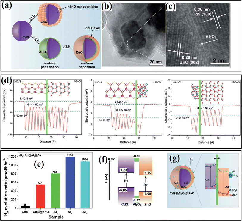 | ||
| Fig. 25 (a) Schematic view of the preparation of Cd@Al@ Zn. (b and c) TEM and HR-TEM images of Cd@Al@ Zn. (d) Calculated slab module of energy change along the c direction of the slab cell for CdS–ZnO, CdS–Al2O3 and Al2O3–ZnO interfaces. (e) Comparison of photocatalytic H2 generation rates over the as-fabricated samples with different deposition thickness of Al2O3. (f) Calculated energy band position of CdS, Al2O3 and ZnO. (g) Possible energy transfer mechanism in Cd@Al@Zn. Reproduced with permission from Ref 57. Copyright 2020, the Royal Society of Chemistry. | ||
Huang et al.109 introduced an Sx–In–P1−x passivation monolayer in the interface between InP and ZnS, where the Sx–In–P1−x monolayer passivated the defects in the original InP, which inhibited the undesirable photogenerated charge recombination at the trap sites and resulted in positive effects for photocatalytic H2 evolution. At the same time, the passivation monolayer decreased the lattice mismatch between the InP core and ZnS shell, further eliminating the interfacial defect sites in the hybrids. Furthermore, the formed alloyed interface also played a vital role in spreading out the radial probability density of electrons and holes, while the delocalization of excitons to the buffer layer was beneficial for their tunneling out of InP.
Another negative effect caused by interfacial stress is the agglomeration of catalysts, which reduces the effective contact between semiconductors and results in a limited interface electric field. Focusing on this issue, by encapsulating SnO2 QDs with a thin carbon layer, Yan et al.62 anchored SnO2 quantum dots (QDs) on the surface of g-C3N4 nanosheets and efficiently avoided the aggregation of SnO2 QDs. As shown in Fig. 26, theoretical calculations revealed that carbon encapsulation can stabilize the SnO2 QDs and strengthen the interaction between SnO2 and g-C3N4 nanosheets, and thus a strong internal electric field can be formed at the intimate interface between SnO2 and g-C3N4, is which beneficial for the separation and one-directional migration of photogenerated charge carriers. To construct a stable contact between FTO glass and photocatalyst, Chen et al.58 deposited an interfacial anatase TiO2 seed layer prior to the growth of rutile TiO2 nanorods, which led to 34% enhanced photocatalytic H2 evolution performance of the sample. The interfacial charge-carrier dynamics studies revealed that the anatase TiO2 seed layer was beneficial for better energy band alignment and boosted charge collection at the interface of TiO2 NR/FTO.
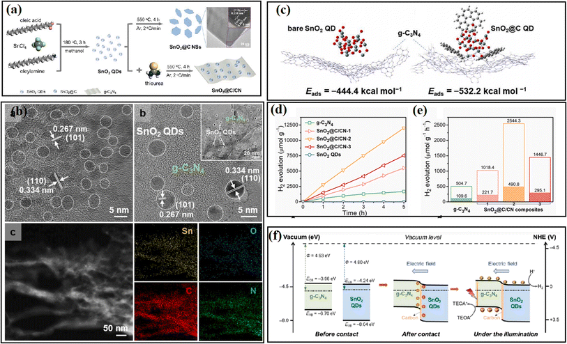 | ||
| Fig. 26 (a) Overview of the synthetic procedure for SnO2@C/CN. TEM image is SnO2@C NSs. (b) TEM image, HRTEM and EDX elemental mapping images of SnO2@C/CN-2. (c) Side-views of the adsorption configurations of (left) bare SnO2 and (right) SnO2@C QDs on g-C3N4 surface. (d) Photocatalytic H2 evolution in 5 h and (e) photocatalytic H2 evolution rate over the samples. (f) Proposed band alignment and mechanism of photocatalytic H2 evolution involved in the SnO2@C/CN. Reproduced with permission from ref. 62. Copyright 2021, Elsevier. | ||
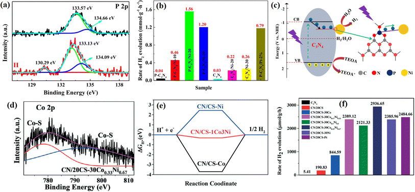 | ||
| Fig. 27 (a) XPS of P 2p in P-C3N4 and P-C3N4/Ni-20. (b) Photocatalytic H2 evolution rates of photocatalysts. (c) Schematic of the photocatalytic H2 production mechanism of P-C3N4/Ni-20. (d) XPS of Co 2p in CN/20CS-30 Co0.33Ni0.67. (e) Gibbs free energy for proton adsorption on CN/CS-Co, CN/CS-1Co3Ni and CN/CS-Ni, and (f) H2 evolution rates of the samples. Reproduced with permission from ref. 60. Copyright 2022, the American Chemical Society. | ||
Besides inserting a thin passivation layer into semiconductors, some impurity atoms can also lead to improved interfacial properties, thus benefiting the photocatalytic reaction. Zhang et al.61 systematically studied the interfacial properties of an MoS2/GaN 2D/3D heterostructure by inserting a nitridation interfacial layer at the MoS2/GaN interface through remote N2 plasma treatment. It was found that the introduction of N atoms efficiently increased the average bond length between the N adatoms and the surface Ga atoms from 2.03 Å to 2.27 Å due to the strong interfacial interaction, where both the CB and VB of MoS2 move upward relative to the GaN side, leading to an increase in the band offsets in this type-II alignment (Fig. 28a and b). At the same time, the introduced indirect band gap caused by N atoms prevented the recombination of photoexcited electrons and holes (Fig. 28c and d). Although the N atoms resulted in a decrease in the band gap of the system, where the CB of the samples was located in the proper position for the splitting of water (Fig. 28e), which indicates an ideal potential in the PHE reaction. More importantly, a notable enhancement in the energy absorption in the range of 2–3 eV was observed for the heterostructure that underwent interface nitridation, implying its potential application as an excellent light harvester (Fig. 28f). This work has demonstrated that treating the interface of heterostructures by using proper atoms is a promising way in efficiently increasing the stability and activity of photocatalysts.
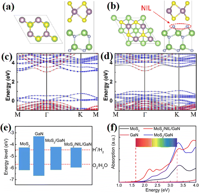 | ||
| Fig. 28 (a and b) Atomic structures of MoS2/GaN heterostructure without and with nitridation interfacial layer. Both the top and side views are demonstrated. (c and d) Corresponding energy band structures. The red (blue) dotted region presents the isolated GaN (MoS2) band structure. (e) Band edge positions of the samples with reference to the vacuum level. (f) Calculated absorption spectra of the samples. Reproduced with permission from ref. 61. Copyright 2018, the American Chemical Society. | ||
Choi and co-workers33 deposited a TiO2 layer between InAs nanowires (NWs) and p-Si by the ALD strategy, and it was found that TiO2 effectively passivated the vulnerable InAs NWs and the Pt co-catalyst prevented the accumulation of photogenerated electrons on the surface of TiO2. In this system, the self-reduction of the TiO2 passivation layer was suppressed by the outer Pt, and thus the obtained catalyst system displayed good stability over 20 h (Fig. 29).
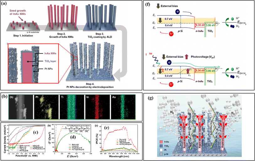 | ||
| Fig. 29 (a) Schematic diagrams of experimental procedures, photographic image, and optical reflectance. (b) HAADF-EDS mapping images of the TiO2/InAs NWs/p-Si photocathode. (For interpretation of the references to colour in this figure legend, the reader is referred to the web version of this article.) (c) J–V curves of the heterostructure photocathodes, (d) EIS spectra and (e) incident-photon-to-current conversion efficiency measurements of the samples. (f) Energy band diagram of the Pt/TiO2/InAs NWs/p-Si photocathodes at 0.48 V vs. RHE under dark (top) and illumination (bottom). (g) Illustration of the H2 evolution mechanism in TiO2/InAs NWs/p-Si. Reproduced with permission from ref. 33. Copyright 2020, Elsevier. | ||
In Devarapalli's34 report, a thin carbon layer was introduced in the interface between Si nanowires (SiNWs) and TiO2 to reduce the number of defect sites and protect against oxidation in the air or water. Specifically, the surface of hydrogen-terminated SiNWs was firstly chemically functionalized using a photochemical alkylation method, and subsequently the functionalized surface was converted into an ultra-thin passivation layer of carbon by annealing at high temperature. The introduced carbon layer efficiently decreased the charge recombination rates and enhanced the interfacial charge transfer between the silicon and TiO2. As shown in Fig. 30a and b, based the observation of flat band potential values, it was confirmed that the carbon passivation layer did not change the properties of silicon except perhaps passivating the defects on the surface of the silicon nanowires. It was found that the donor densities (Nd) for C@SiNWs were an order of magnitude higher than that for SiNWs, demonstrating that the introduction of a carbon passivation layer resulted in higher carrier generation and lower recombination losses. In addition, the corresponding photoelectric chemical performance tests showed that the carbon-modified sample displayed much higher photoelectric transfer ability (Fig. 30c and d). The formation of a carbon layer efficiently suppressed the recombination of electrons and holes, reduced the number of defect sites, and improved the interfacial charge transfer between SiNWs and TiO2. As a result, the optimized sample displayed 2.78 times higher water splitting efficiency than that on the non-passivated sample.
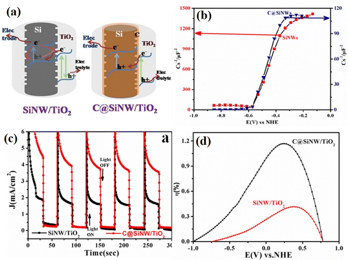 | ||
| Fig. 30 (a) Proposed electron transfer mechanism in SiNW/TiO2 and C@SiNW/TiO2 core–shell nanowire arrays. (b) Mott–Schottky plots of SiNWs and C@SiNWs measured at 5 kHz. (c) Chronoamperometric graphs under light off and on conditions of C@SiNWs/TiO2 and SiNWs/TiO2 nanowires. (d) Photoconversion efficiencies of the samples as a function of measured potentials. Reproduced with permission from ref. 34. Copyright 2014, Springer. | ||
In summary, the formation of a well-contacted interface in an interfacial passivation system is mainly due to the special structures of the passivation layer or the existence of strong chemical bonding between the passivation layer and substrates. In general, there are two types of materials that can be utilized for interfacial passivation. (1) Materials with an amorphous crystal structure, in which the loose and irregular arrangement of atoms endows the material with good surface compatibility. When combined with semiconductors, the adjustable arrangement of atoms guarantees the formation of an intimately contacted semiconductor-passivation layer interface at the atomic level. Subsequently, when a secondary semiconductor is introduced, a well-contacted passivation layer-semiconductor interface will be formed at the other side of the passivation layer. Thus, the passivation layer serves as an interfacial bridge to provide a soft buffer region and efficiently release the interfacial stress between directly contacted semiconductors. (2) Materials capable of forming strong chemical bonds with semiconductors. During some special treatment procedures, such as high temperature, the formation of strong chemical bonding efficiently declines the density of defects and serves as a bonding bridge between two semiconductors, thus contributing to the formation of a well-contacted interface.
5.3 Key factors and strategies controlling the influence of the effect of passivation engineering
Based on numerous reports, it can be found that the passivation layer often functions as a double-edged sword, and thus it cannot be concluded that the presence of a passivation layer with result in a higher photocatalytic performance. Many materials used in passivation engineering are inert or only have very low activity in PHE, and the introduction of a surplus passivation layer will lead to an increase in the proportion of non-active components, which not only leads to a decline in photocatalytic activity at the same mass, but also increases the catalytic cost.81,90,92 Moreover, most of the passivation materials are not universal in all systems, and the materials that show an enhanced effect on some substrates may lead to a decrease in catalytic performance on others, which depends on the basic electrochemical properties of passivation materials and interaction between the passivation layer and the substrates. It can be seen that the thickness and type of passivation materials are the two dominant factors that should be considered. In the following content, we will give a detailed introduction on the influence of these two key factors on the passivation layer and the regulation strategies.The ALD method is regarded as one of the most efficient methods for precisely controlling the thickness of the passivation layer, by which the covering thickness can be changed at the atomic level due to the self-limited deposition property through the deposition cycle times. ALD can be used in the formation of both surface passivation and interfacial passivation layers and their thickness. For example, Liu and coworkers111 deposited a TiO2 shell on ZnO nano-arrays through the ALD method, and a nearly 90% declined deep-level PL emission could be achieved when the thickness of TiO2 decreased to about 1 nm, indicating the efficient removal of the deep hole traps through the surface passivation. In another example,55 an ALD method was utilized to deposit a TiO2 passivation layer between CdS and ZnO, and a 20 nm passivation TiO2 layer was found to be the most efficient in obtaining the highest H2 evolution ability. In our previous work,57 by changing the ALD deposition cycle from 1, 2, 4, to 10 times, it was found that an ultrathin passivation layer with 2 cycles of Al2O3 deposition resulted in the most improved H2 evolution rate.
Some other deposition methods, such as chemical vapor deposition (CVD) and ion sputtering method, are also utilized for the introduction of a passivation layer, and the deposition cycle and deposition times are two crucial parameters in controlling the thickness of the passivation layer. In 2013, Seger et al.112 modified Si-based photoelectrodes using TiO2 as a conductive passivation layer. The thickness of the TiO2 layer could be controlled by the sputtering time, and a sputtered 100 nm passivation layer was proven to be the most effective in protecting the surface of the Si substrate from corrosion.
In addition to deposition strategies, high-temperature treatment is also a common method in passivation engineering. For example, in the reported CdS/CdZnS/ZnO system,63 the CdZnS passivation layer was formed at the interface between CdS and ZnO under high-temperature condition, with the gradual consumption of CdS and ZnO. The heating temperature had an obvious effect on the formation and content of the passivation layer. When the heating temperature was too low, the formation of CdZnS was too small to totally passivate the interface defects between CdS and ZnO, but a too high temperature led to a dramatically declined PHE performance due to the over consumption of photocatalytic active components (CdS and ZnO). Similarly, in the work by Yan and coworkers,62 the relative content of carbon passivation layer in an SnO2 QD-deposited g-C3N4 system could be controlled by tuning the additive amount of precursors. However, in these heating strategies, it is difficult to precisely control to the thickness of the passivation layer. By controlling some key parameters, such as additive amount of precursors, the reaction time, and reaction temperature, the relative content of passivation layer can be controlled in a qualitative aspect.
To date, the study on the effect of materials on passivation engineering has mainly focused on the ion-induced surface passivation system. Liu et al.104 studied the effect of edge passivation of halogen ions on the PHE of Sb nanoribbons. In all the samples, the introduction of halogen ions is useful for improving the stability and benefiting the light absorption. At the same time, the halogen ions display different tuning effects in changing the band edges and band gaps of Sb, and only the F-decorated sample matched the REDOX potentials of PHE. Agrawal et al.113 studied the influence of halogen (F, Cl, Br, and I) passivation on the electronic structure of zigzag graphene nanoribbons (ZGNRs). They found that the stability of the halogen-passivated ZGNRs followed the order of F > Cl > Br > I, while the I- and Br-passivated samples had relatively higher current–voltage characteristics than the F- and Cl-passivated samples. Neuderth and coworkers90 studied the influence of ultra-thin TiO2, CeO2 and Al2O3 passivation layers on the photocatalytic properties of InGaN. They found that the 5 nm TiO2-passivated sample displayed an increase in anodic photocurrent, whereas a decreased photocurrent was observed for the CeO2- and Al2O3-coated sample due to the enhanced defect recombination in the passivation layer or increased band discontinuities. Furthermore, the photocatalytic ability of the InGaN NW decreased due to the TiO2 layer and was even completely suppressed when the thickness of the TiO2 layer reached to 7 nm or more. This work fully demonstrated the important influence of the type and thickness of the passivation layer materials on the properties of the substrate materials.
In addition, it is foreseeable that the impact of passivation materials on the passivation effect is also reflected in the type and strength of the interaction between the passivation layer and the substrate. However, to the best of our knowledge, there is still lack of systematic study on the relationship between the types of materials in the passivation layer and their passivation effect. With the development of passivation engineering in the photocatalytic field, we believe that related studies will be reported in the near future.
6. Conclusions and outlook
Photocatalytic hydrogen evolution provides an eco-friendly and sustainable pathway to address the issues related to the energy and environment, but the low activity and poor stability of photocatalysts have long restricted the promotion and application of PHE technology. In this case, passivation is an efficient and promising strategy in protecting the vulnerable surface from the environment and buffering the recombination of charges from the defective interface. Focusing on the various problems in different catalysts, different passivation methods can be adopted to eliminate the defects, protect the susceptible surface, and construct an intimately contacted interface, thus suppressing the harmful charge recombination and photo-corrosion, and ultimately improving the photocatalytic activity and durability of catalysts. This review presented a comprehensive overview of passivation engineering ranging from its basic principles, roles, fabrication methods, and characterization methods to its application in interfacial passivation and surface passivation. However, despite the significant advances to date, the study of passivation technology is still limited. Thus, to make full use of passivation engineering to improve the performance of photocatalysts, the following factors are worth exploring in future studies.(1) There is still much debate regarding the mechanism of passivation-modified catalysts, especially in core–shell structure photocatalysts. Some researchers ascribe the improvement in hydrogen evolution ability to the formation of a heterostructure but ignore the passivation effect caused by the covering layer, while other researchers tend to emphasize the role of the shell in eliminating defects or suppressing charge recombination as a passivation layer, but the photocatalytic ability of the passivation layer itself is neglected. Therefore, to comprehensively reveal the mechanism of photocatalysis, the existence of a passivation layer and its effects need to be accurately identified and fully verified.
(2) The introduction of passivation engineering is useful in improving the photocatalytic performance, but the control and optimization of the passivation degree still require significant efforts. As mentioned, some defects can be eliminated through the appropriate passivation treatment, but it was also reported that the existence of defects contributes to the separation of charge carriers. In this case, it is a challenge to accurately detect the type and function of defects and eliminate unfavorable defects and retain favorable defects by appropriate passivation means.
(3) Characterization methods still lag behind the development of synthetic methods, which presents an obstacle in investigating the effects and mechanisms of passivation engineering. For instance, the formation, spatial distribution and concentration of surface and interface defects have a deadly effect on the transfer and separation of charge carriers, but these features still cannot be accurately characterized by prior characterization means. In addition, to deepen the understanding on the contribution of passivation engineering to photocatalytic performance, some in situ studies at high spatial and temporal resolutions are also urgently needed.
(4) Although ALD is widely adopted in the deposition of a passivation layer, the large-scale use of this technology is still unrealistic in a short time because of the high-cost precursors and trivial technological operation. Thus, new methods need to be developed to construct passivation systems with high efficiency, good controllability and low cost.
Conflicts of interest
The authors declare no conflict of interest.Acknowledgements
This work was sponsored by the National Natural Science Foundation of China (21972110), the Postdoctoral Science Foundation of China (2021M692535), the Natural Science Foundation of Shaanxi Province (2022JQ-095), the Basic Research Project Foundation of Xi'an Jiaotong University (xzy012024012), and the Youth Foundation of State Key Laboratory of Electrical Insulation and Power Equipment (EIPE2131).References
- M. Qi, M. Conte, M. Anpo, Z. Tang and Y. Xu, Chem. Rev., 2021, 121, 13051–13085 CrossRef CAS PubMed.
- Y. Li, S. Yu, J. Xiang, F. Zhang, A. Jiang, Y. Duan, C. Tang, Y. Cao, H. Guo and Y. Zhou, ACS Catal., 2023, 13, 8281–8292 CrossRef CAS.
- M. Rahman, T. Edvinsson and J. Gascon, Nat. Rev. Chem., 2022, 6, 243–258 CrossRef PubMed.
- Q. Wang and K. Domen, Chem. Rev., 2020, 120, 919–985 CrossRef CAS PubMed.
- D. Maarisetty and S. Baral, J. Mater. Chem. A, 2020, 8, 18560 RSC.
- Z. Kang, H. Si, S. Zhang, J. Wu, Y. Sun, Q. Liao, Z. Zhang and Y. Zhang, Adv. Funct. Mater., 2019, 29, 1808032 CrossRef.
- X. Wang, C. Zhou, W. Wang, B. Du, J. Cai, G. Feng and R. Zhang, J. Alloys Compd., 2018, 747, 826–833 CrossRef CAS.
- H. Ren, K. Ye, H. Chen, F. Wang, Y. Hu, Q. Shi, H. Yu, R. Lv and M. Chen, Colloids Surf., A, 2022, 652, 129844 CrossRef CAS.
- G. Cheng, S. Li, C. Wang and J. Xiong, Adv. Energy Sustainability Res., 2023, 4(7), 2300002 CrossRef CAS.
- D. Ma, J. Shi, L. Sun, Y. Sun, S. Mao, Z. Pu, C. He, Y. Zhang, D. He, H. Wang and Y. Cheng, Chem. Eng. J., 2022, 431, 133446 CrossRef CAS.
- R. Singh and S. Dutta, Fuel, 2018, 220, 607–620 CrossRef CAS.
- W. Ma, D. Zheng, B. Xiao, Y. Xian, Q. Zhang, S. Wang, J. Liu, P. Wang and X. Hu, J. Environ. Chem. Eng., 2022, 10(3), 107822 CrossRef CAS.
- L. Cheng, Q. Xiang, Y. Liao and H. Zhang, Energy Environ. Sci., 2018, 11, 1362–1391 RSC.
- Y. Zou, J. Shi, D. Ma, Z. Fan, C. He, L. Cheng, D. Sun, J. Li, Z. Wang and C. Niu, Catal. Sci. Technol., 2018, 8, 3883–3893 RSC.
- Y. Zhi, Y. Yi, C. Deng, Q. Zhang, S. Yang and F. Peng, ChemSusChem, 2022, 15, e202200860 CrossRef CAS PubMed.
- G. Lee and J. Wu, Powder Technol., 2017, 318, 8–22 CrossRef CAS.
- C. Chang, K. Chu, M. Hsu and C. Chen, Int. J. Hydrogen Energy, 2015, 40, 14498–14506 CrossRef CAS.
- J. Shi, Y. Zou, D. Ma, Z. Fan, L. Cheng, D. Sun, Z. Wang, C. Niu and L. Wang, Nanoscale, 2018, 10, 9292–9303 RSC.
- J. Shi, Y. Zou, L. Cheng, D. Ma, D. Sun, S. Mao, L. Sun, C. He and Z. Wang, Chem. Eng. J., 2019, 378, 122161 CrossRef CAS.
- S. Mao, J. Shi, G. Sun, Y. Zhang, D. Ma, K. Song, Y. Lv, J. Zhou, H. Wang and Y. Cheng, ACS Appl. Mater. Interfaces, 2022, 14, 48770–48779 CrossRef CAS PubMed.
- Y. Lv, D. Ma, C. Yang, K. Song, L. Shi, Y. Cheng, C. Niu and J. Shi, Sep. Purif. Technol., 2023, 316, 123813 CrossRef CAS.
- P. Madhusudan, Y. Wang, B. Chandrashekar, W. Wang, J. Wang, J. Miao, R. Shi, Y. Liang, G. Mi and C. Cheng, Appl. Catal., B, 2019, 253, 379–390 CrossRef CAS.
- J. Lin, Y. Yan, T. Xu, J. Cao, X. Zheng, J. Feng and J. Qi, J. Colloid Interface Sci., 2020, 564, 37–42 CrossRef CAS PubMed.
- C. Liu, T. Gong, J. Zhang, X. Zheng, J. Mao, H. Liu, Y. Lia and Q. Hao, Appl. Catal.; B, 2020, 262, 118245 CrossRef CAS.
- Y. Lv, D. Ma, K. Song, S. Mao, Z. Liu, D. He, X. Zhao, T. Yao and J. Shi, J. Mater. Chem. A, 2023, 11, 800–808 RSC.
- S. Mao, J. Shi, G. Sun, Y. Zhang, X. Ji, Y. Lv, B. Wang, Y. Xu and Y. Cheng, Chem. Eng. J., 2021, 404, 126533 CrossRef CAS.
- D. Ma, J. Shi, Z. Pu, S. Mao, X. Xu, D. He, R. Guo and F. Chen, Sol. RRL, 2022, 6, 2200714 CrossRef CAS.
- Y. Yang, Y. Liu, B. Mao, B. Luo, K. Zhang, W. Wei, Z. Kang, W. Shi and S. Yuan, Catal. Lett., 2019, 149, 1800–1812 CrossRef CAS.
- S. Yang, D. Prendergast and J. Neaton, Nano Lett., 2012, 12, 383–388 CrossRef CAS PubMed.
- C. Li, M. Gao, X. Sun, H. Tang, H. Dong and F. Zhang, Appl. Catal., B, 2020, 266, 118586 CrossRef CAS.
- R. Zhong, Z. Zhang, H. Yi, L. Zeng, C. Tang, L. Huang and M. Gu, Appl. Catal., B, 2018, 237, 1130–1138 CrossRef CAS.
- Q. Gai, S. Ren, X. Zheng, W. Liu and Q. Dong, Catal. Sci. Technol., 2021, 11, 5579–5589 RSC.
- S. Choi, J. Hwang, T. Lee, H. Kim, S. Hong, C. Kim, M. Choi, H. Park, S. Bhat, J. Suh, J. Lee, K. Choi, S. Hong, J. Shin and H. Jang, Chem. Eng. J., 2020, 392, 123688 CrossRef CAS.
- R. Devarapalli, J. Debguptal, V. Pillai and M. Shelke, Sci. Rep., 2014, 4, 4897 CrossRef CAS PubMed.
- H. Cheng, F. Wang, J. Chu, R. Santhanam, J. Rick and S. Lo, J. Phys. Chem. C, 2012, 116, 7629–7637 CrossRef CAS.
- N. Elumalai, C. Vijila, R. Jose, A. Uddin and S. Ramakrishna, Mater. Renew. Sustain. Energy, 2015, 4, 11 CrossRef.
- C. Han, P. Su, B. Tan, X. Ma, H. Lv, C. Huang, P. Wang, Z. Tong, G. Li, Y. Huang and Z. Liu, J. Colloid Interface Sci., 2021, 581, 159–166 CrossRef CAS PubMed.
- Y. Yu, W. Yan, X. Wang, P. Li, W. Gao, H. Zou, S. Wu and K. Ding, Adv. Mater., 2018, 30, 1705060 CrossRef PubMed.
- C. Lee, L. Hung, Y. Shih, J. Wu, S. Wang, C. Huang and V. Nguyen, J. Environ. Chem. Eng., 2021, 9, 104826 CrossRef CAS.
- M. Zhu, F. Zhang and Y. Wang, New J. Chem., 2022, 46, 16243–16255 RSC.
- P. Sudhagar, A. Devadoss, K. Nakata, C. Terashima and A. Fujishim, J. Electrochem. Soc., 2015, 162(3), 108–114 CrossRef.
- H. Le, M. Nguyen, Y. Pham, D. Nguyen, L. Le, H. Han and P. Tran, Mater. Today Energy, 2021, 21, 100762 CrossRef CAS.
- S. Kumar, S. Ahirwarc and A. Satpati, RSC Adv., 2019, 9, 41368 RSC.
- Y. Chen, Y. Chen, J. Chen, F. Cao, L. Li, Z. Luo, I. Leu and Y. Pu, ACS Appl. Mater. Interfaces, 2019, 11, 8126–8137 CrossRef CAS PubMed.
- J. Yang, W. Liao and J. Wu, ACS Appl. Mater. Interfaces, 2013, 5, 7425–7431 CrossRef CAS PubMed.
- R. Zhang, M. Shao, S. Xu, F. Ning, L. Zhou and M. Wei, Nano Energy, 2017, 33, 21–28 CrossRef CAS.
- Y. Hwang, C. Hahn, B. Liu and P. Yang, ACS Nano, 2012, 6, 5060–5069 CrossRef CAS PubMed.
- A. Dey, G. Chandrabosea, L. Dampteya, E. Erakulanb, R. Thapa, S. Zhukc, G. Dalapatia, S. Ramakrishnad, N. Braithwaitea, A. Shirzadia and S. Krishnamurthy, Appl. Surf. Sci., 2020, 541, 148571 CrossRef.
- I. Daskalakis, I. Vamvasakis, I. Papadas, S. Tsatsos, S. Choulis, S. Kennouc and G. Armatas, Inorg. Chem. Front., 2020, 7, 4687 RSC.
- K. Alam, P. Kumar, P. Kar, U. Thakur, S. Zeng, K. Cui and K. Shankar, Nanoscale Adv., 2019, 1, 1460–1471 RSC.
- S. Kang, S. Li, T. Pu, X. Fang, C. Yin, M. Dong and L. Cui, Int. J. Hydrogen Energy, 2018, 43, 22265–22272 CrossRef CAS.
- S. Zhang, Z. Liu, W. Yan, Z. Guo and M. Ruan, Chin. J. Catal., 2020, 41, 1884–1893 CrossRef CAS.
- B. Seger, T. Pedersen, A. Laursen, P. Vesborg, O. Hansen and I. Chorkendorff, J. Am. Chem. Soc., 2013, 135, 1057–1064 CrossRef CAS PubMed.
- E. Cowell, N. Alimardani, C. Knutson, J. Jr, D. Keszler, B. Gibbons and J. Wager, Adv. Mater., 2011, 23, 74–78 CrossRef CAS PubMed.
- Z. Bai, X. Yan, Y. Li, Z. Kang, S. Cao and Y. Zhang, Adv. Energy Mater., 2016, 6, 1501459 CrossRef.
- M. Feng, Y. Liu, N. Wei, S. Ma, Z. Li, H. Li, S. Chen, J. Liu and D. Wang, J. Mater. Chem. A, 2018, 6, 18293–18303 RSC.
- D. Ma, Z. Wang, J. Shi, Y. Zou, Y. Lv, X. Ji, Z. Li, Y. Cheng and L. Wang, J. Mater. Chem. A, 2020, 8, 11031–11042 RSC.
- Y. Chen, Y. Chen, J. Chen, F. Cao, L. Li, Z. Luo, I. Leu and Y. Pu, ACS Appl. Mater. Interfaces, 2019, 11, 8126–8137 CrossRef CAS PubMed.
- Z. Luo, T. Wang, J. Zhang, C. Li, H. Li and J. Gong, Angew. Chem., Int. Ed., 2017, 56(42), 12878–12882 CrossRef CAS PubMed.
- X. Zheng, Y. Wang, S. Ren, Q. Gai, W. Liu and Q. Dong, ACS Appl. Energy Mater., 2022, 5, 5756–5765 CrossRef CAS.
- Z. Zhang, Q. Qian, B. Li and K. Chen, ACS Appl. Mater. Interfaces, 2018, 10, 17419–17426 CrossRef CAS PubMed.
- J. Yan, Z. Song, H. Li, H. Xu and L. Lee, Chem. Eng. J., 2021, 425, 131512 CrossRef CAS.
- H. Nan, W. Wu, K. Feng, B. Shan, Y. Qiu and Y. Zhang, Int. J. Hydrogen Energy, 2017, 42, 848–857 CrossRef CAS.
- L. Steier, I. Herraiz-Cardona, S. Gimenez, F. Santiago, J. Bisquert, S. Tilley and M. Grätzel, Adv. Funct. Mater., 2014, 24, 7681–7688 CrossRef CAS.
- X. Xiao, X. Wang, Y. Li, Y. Li, G. Sun and Y. Han, Appl. Surf. Sci., 2023, 631, 157577 CrossRef CAS.
- C. Liu, C. Zhang, G. Yin, T. Zhang, W. Wang, G. Ou, H. Jin and Z. Chen, ACS Appl. Mater. Interfaces, 2021, 13, 13301–13310 CrossRef CAS PubMed.
- J. Kim, Appl. Sci., 2018, 8, 1402 CrossRef.
- A. Ghobadi, T. Ulusoy, R. Garifullin, M. Guler and A. Okyay, Sci. Rep., 2016, 6, 30587 CrossRef CAS PubMed.
- S. Mali, C. Shim, H. Park, J. Heo, P. Patil and C. Hong, Chem. Mater., 2015, 27, 1541–1551 CrossRef CAS.
- Y. Wang, W. Bai, S. Han, H. Wang, Q. Wu, J. Chen, G. Jiang, Z. Zhao, C. Xu and Q. Huan, Curr. Catal., 2017, 6, 50–56 CrossRef CAS.
- S. Li, P. Zhang, X. Song and L. Gao, ACS Appl. Mater. Interfaces, 2015, 7, 18560–18565 CrossRef CAS PubMed.
- R. Rather, S. Singh and B. Pal, Appl. Catal., B, 2017, 213, 9–17 CrossRef CAS.
- M. Park, J. Jung, Y. Nam, J. Song, C. Jeong and J. Lee, Thin Solid Films, 2016, 616, 550–554 CrossRef CAS.
- M. Park, J. Jung, S. Shin, J. Song, Y. Nam, D. Kim and J. Lee, Thin Solid Films, 2016, 599, 54–58 CrossRef CAS.
- S. Chen, Y. Qi, Q. Ding, Z. Li, J. Cui, F. Zhang and C. Li, J. Catal., 2016, 339, 77–83 CrossRef CAS.
- M. Rehman, I. Akhtar, W. Choi, K. Akbar, A. Farooq, S. Hussain, M. Shehzad, S. Chun, J. Jung and Y. Seo, Carbon, 2018, 132, 157–164 CrossRef.
- Q. Cheng, M. Benipal, Q. Liu, X. Wang, P. Crozier, C. Chan and R. Nemanich, ACS Appl. Mater. Interfaces, 2017, 9, 16138–16147 CrossRef CAS PubMed.
- S. Nayak and K. Parida, Sci. Rep., 2019, 9, 2458 CrossRef PubMed.
- C. Sakdaronnarong, A. Sangjan, S. Boonsith, D. Kim and H. Shin, Catalysts, 2020, 10, 320 CrossRef CAS.
- Z. Shen, M. Cheng, Y. Yuan, L. Pei, J. Zhong, J. Guan, X. Li, Z. Li, L. Bao, X. Zhang, Z. Yu and Z. Zou, Appl. Catal., B, 2021, 295, 120274 CrossRef CAS.
- P. Zhao, Y. Li, L. Li, S. Bu and W. Fan, J. Phys. Chem. C, 2018, 122, 10737–10748 CrossRef CAS.
- S. Wang, Y. Zhang, Y. Zheng, Y. Xu, G. Yang, S. Zhong, Y. Zhao and S. Bai, Small, 2023, 19, 2204774 CrossRef CAS PubMed.
- S. Zheng, L. Han, X. Luo, L. Sun, N. L, Z. Zhang and X. Li, Int. J. Energy Res., 2022, 46, 4506–4515 CrossRef CAS.
- X. Wu, X. Wang, Y. Xie, N. Ren, J. Ma and P. Ning, Appl. Catal., B, 2022, 310, 121325 CrossRef CAS.
- W. Yang, L. Zhang, J. Xie, X. Zhang, Q. Liu, T. Yao, S. Wei, Q. Zhang and Y. Xie, Angew. Chem., Int. Ed., 2016, 55(23), 6716–6720 CrossRef CAS PubMed.
- Y. Zhao, G. Chen, T. Bian, C. Zhou, G. I. N. Waterhouse, L. Z. Wu, C. H. Tung, L. J. Smith, D. O'Hare and T. Zhang, Adv. Mater., 2015, 27, 7824 CrossRef CAS PubMed.
- X. Chen, L. Liu, Z. Liu, M. A. Marcus, W. C. Wang, N. A. Oyler, M. E. Grass, B. Mao, P. A. Glans, P. Y. Yu, J. Guo and S. S. Mao, Sci. Rep., 2013, 3, 1510 CrossRef PubMed.
- Y. Chen, Y. Chen, J. Chen, F. Cao, L. Li, Z. Luo, I. Leu and Y. Pu, ACS Appl. Mater. Interfaces, 2019, 11, 8126–8137 CrossRef CAS PubMed.
- K. M. Alam, C. E. Jensen, P. Kumar, R. W. Hooper, G. M. Bernard, A. Patidar, A. P. Manuel, N. Amer, A. Palmgren, D. N. Purschke, N. Chaulagain, J. Garcia, P. S. Kirwin, L. C. T. Shoute, K. Cui, S. Gusarov, A. E. Kobryn, V. K. Michaelis, F. A. Hegmann and K. Shankar, ACS Appl. Mater. Interfaces, 2021, 13, 47418–47439 CrossRef CAS PubMed.
- P. Neuderth, P. Hille, J. Schörmann, A. Frank, C. Reitz, S. Martí-Sánchez, M. De, M. Coll, J. Arbiol, R. Marschall and M. Eickhoff, J. Mater. Chem. A, 2018, 6, 565 RSC.
- M. Kim, B. Joshi, E. Samuel, H. Seok, A. Aldalbahi, M. Almoiqli, M. Swihart and S. Yoon, Appl. Catal., B, 2020, 271, 118928 CrossRef CAS.
- K. Rasamani, Z. Li and Y. Sun, Nanoscale, 2016, 8, 18621 RSC.
- C. Chen, P. Chen, M. Basu, K. Yang, Y. Lu, C. Dong, C. Ma, C. Shen, S. Hu and R. Liu, J. Mater. Chem. A, 2015, 3, 23466 RSC.
- S. Chen, X. Lia, W. Zhou, S. Zhang and Y. Fang, Appl. Surf. Sci., 2019, 466, 254–261 CrossRef CAS.
- B. Zhang, T. Yu, Y. Liu, M. Feng, X. Li, W. Sun and D. Wang, Chem. Eng. J., 2022, 429, 132248 CrossRef.
- J. Qiu, G. Zeng, M. Ge, S. Arab, M. Mecklenburg, B. Hou, C. Shen, A. Benderskii and S. Cronin, J. Catal., 2016, 337, 133–137 CrossRef CAS.
- X. Zhang, G. Lu, Y. Wu, J. Dong and C. Wang, Catal. Sci. Technol., 2021, 11, 5505 RSC.
- X. Yu, J. Xie, Q. Liu, H. Dong and Y. Li, J. Colloid Interface Sci., 2021, 593, 133–141 CrossRef CAS PubMed.
- Y. Ben-Shahar, F. Scotognella, N. Waiskopf, I. Kriegel, S. Conte, G. Cerullo and U. Banin, Small, 2015, 11(4), 462–471 CrossRef CAS PubMed.
- N. Hewa-Kasakarage, M. Kirsanova, A. Nemchinov, N. Schmall, P. El-Khoury, A. Tarnovsky and M. Zamkov, J. Am. Chem. Soc., 2009, 131, 1328–1334 CrossRef CAS PubMed.
- A. Thibert, F. Frame, E. Busby, M. Holmes, F. Osterloh and D. Larsen, J. Phys. Chem. Lett., 2011, 2, 2688–2694 CrossRef CAS.
- P. Tongying, V. Plashnitsa, N. Petchsang, F. Vietmeyer, G. Ferraudi, G. Krylova and M. Kuno, J. Phys. Chem. Lett., 2012, 3, 3234–3240 CrossRef CAS PubMed.
- W. Kim, J. Kim, S. Lee, S. Lee, J. Woo, K. Lee, W. Chae, S. Jeong, W. Bae, J. McGuire, J. Moon, M. Jeong and D. Lee, Chem. Mater., 2016, 28, 962–968 CrossRef CAS.
- M. Liu, C. Yang, M. Wang and X. Ma, J. Phys. Chem. C, 2021, 125, 21341–21351 CrossRef CAS.
- J. Xiong, J. Di, J. Xia, W. Zhu and H. Li, Adv. Funct. Mater., 2018, 28(39), 1801983 CrossRef.
- Y. Huang, L. Meng, W. Xu and L. Li, Adv. Funct. Mater., 2023, 33(47), 2305940 CrossRef CAS.
- K. Dai, L. Lu, C. Liang, G. Zhu, Q. Liu, L. Geng and J. He, Dalton Trans., 2015, 44, 7903–7910 RSC.
- Z. Zhang, M. Choi, M. Baek, I. Hwang, C. Cho, Z. Deng, J. Lee and K. Yong, Nano Res., 2017, 10, 2415–2430 CrossRef CAS.
- R. Huang, Z. Qin, L. Shen, G. Lv, F. Tao, J. Wang and Y. Gao, J. Mater. Chem. A, 2023, 11, 6217–6225 RSC.
- E. W. Cowell, N. Alimardani, C. C. Knutson, J. F. Conley, D. A. Keszler, B. J. Gibbons and J. F. Wager, Adv. Mater., 2011, 23(1), 74–78 CrossRef CAS PubMed.
- M. Liu, C. Y. Nam, C. T. Black, J. Kamcev and L. Zhang, J. Phys. Chem. C, 2013, 117, 13396 CrossRef CAS.
- B. Seger, T. Pedersen, A. B. Laursen, P. C. K. Vesborg, O. Hansen and I. Chorkendorff, J. Am. Chem. Soc., 2013, 135, 1057–1064 CrossRef CAS PubMed.
- S. Agrawal, A. Srivastava and G. Kaushal, Semicond. Sci. Technol., 2022, 37, 025004 CrossRef.
- F. Li, J. Jian, S. Wang, Z. Zhang, X. Guan, Y. Xu and H. Wang, Chem. Eng. J., 2023, 461, 141872 CrossRef CAS.
- P. Zhao, Y. Li, L. Li, S. Bu and W. Fan, J. Phys. Chem. C, 2018, 122, 10737–10748 CrossRef CAS.
- B. He, R. Liu, J. Ren, C. Tang, Y. Zhong and Y. Hu, Langmuir, 2017, 33, 6719–6726 CrossRef CAS PubMed.
- X. Bao and L. Liu, J. Power Sources, 2014, 268, 677–682 CrossRef CAS.
- X. Wu, X. Wang, Y. Xie, N. Ren, J. Ma and P. Ning, Appl. Catal., B, 2022, 310, 121325 CrossRef CAS.
- X. Ning, W. Zhen, X. Zhang and G. Lu, ChemSusChem, 2019, 12, 1410–1420 CrossRef CAS PubMed.
- H. Guo, B. Luo, J. Wang, B. Wang, X. Huang, J. Yang, W. Gong, Y. Zhou and X. Niu, J. Mater. Chem. A, 2020, 8, 24655–24663 RSC.
| This journal is © The Royal Society of Chemistry 2024 |

