Phase engineering to construct In2S3 heterophase junctions and abundant active boundaries and surfaces for efficient Pyro-PEC performance in CdS/In2S3†
Xingfei
Chen
a,
Mengnan
Ruan
ab,
Chengyi
Wang
ab,
Tingting
Zhong
ab and
Zhifeng
Liu
 *ab
*ab
aSchool of Materials Science and Engineering, Tianjin Chengjian University, 300384, Tianjin, China. E-mail: tjulzf@163.com; Tel: +86 22 23085236
bTianjin Key Laboratory of Building Green Functional Materials, 300384, Tianjin, China
First published on 8th May 2024
Abstract
Metal sulfide photoelectrodes are considered as common catalysts for PEC water splitting, but their instability and carrier density limitations still restrict their applications. Phase modification plays a vital role in improving photocatalytic efficiency. Here, we successfully constructed In2S3 heterophase junctions in CdS/In2S3 heterojunctions by phase modulation engineering for efficient pyro-photoelectrochemical catalytic (Pyro-PEC) water splitting. The experimental results show that the CdS/In2S3 generated by phase engineering displays a high current density of 3.52 mA cm−2 at 1.23 V vs. RHE under the Pyro-PEC conditions, which is a 14.67-fold enhancement of bare CdS under the photoelectrocatalytic conditions, and exhibits a 63.98% bulk transport capacity, which is a 49.51% enhancement of bare CdS under photoelectrocatalytic conditions, and the stability also improved very well. This is due to the fact that photoelectrodes with heterojunctions and heterophase junctions formed abundant phase boundaries and active surfaces to promote catalytic reactions, and enhanced the polarization force to optimize the pyroelectric performance, which ultimately achieved excellent pyro-photoelectrochemical performance. This work provides evidence for the effect of phase engineering on photoelectric and pyroelectric properties, and provides a simple and effective method for modulating the phase structure for photoanodes using hydrothermal methods.
1 Introduction
Researchers are continuously working to develop efficient, stable and sustainable energy systems to address the problems of limited conventional energy storage, which are harmful to the environment, and to reduce dependence on finite fossil fuel resources to meet the energy demand.1–3 Hydrogen is a clean and renewable energy source, storing several times more energy per unit mass than fossil fuels, and can be used in industrial fuels, medical anesthesia, and transportation, which is crucial for promoting the energy transition.4–6 Photoelectrochemical (PEC) water splitting utilizes renewable energy sources, such as solar energy, to convert water into hydrogen for highly energy-dense storage and utilization.7 Semiconductors are an influential part of the PEC water splitting and can be categorized into n-type (α-Fe2O3,8–10 CdS,11,12 BiVO4 (ref. 13–15)) and p-type (Sb2S3,16–18 CuFe2O4,19,20 CuO (ref. 21–23)) semiconductors depending on the majority charge carriers. Ideal semiconductors are characterized by high light-absorbing capacity, stable chemical properties, and good catalytic performance. CdS is a candidate for photoanode materials due to its good visible light response and suitable band edge position. However, its stability and catalytic efficiency are not satisfactory, and there are still some challenges.Researchers have put forward the concepts of defect modulation, heterojunction construction, and co-catalysts to enhance the performance of CdS.24–26 For example, Wang et al. investigated the effect of different concentrations of Cu doping on the properties of CdS, and the current density increased to 3.16 mA cm−2 at about 0.75 V.26 Peng et al. regulated the charge migration mode by constructing CdS/MoS2, and the formation of MoS2 in the surface layer not only enhanced the light absorption but also reduced the carrier recombination and optimized the carrier transport regime.27 Chen et al. achieved a large hydrogen precipitation rate of 102.7 μmol h−1 g−1 by using deflected graphene (D-rGO) as a co-catalyst to enhance the catalytic activity and stability of CdS.28 All these behaviors improved the properties of CdS but, unluckily, the limited success of these modification methods remains a matter of concern and new strategies are urgently needed.
It is worth emphasizing that increasing the energy source of the PEC system is an effective means to broaden the applications. In addition to light energy, heat energy from temperature differences is also worth utilizing.29–31 CdS as a pyroelectric material can effectively convert thermal energy into electrical energy, with the advantages of repeated utilization and wide temperature response range. Therefore, the pyro-photoelectrocatalytic (Pyro-PEC) system can increase the driving force of the catalytic system. Among pyroelectric materials, ferroelectrics are a special type of pyroelectric material in which internal spontaneous polarization promotes carrier separation to boost catalytic efficiency.32 Tetragonal-phase In2S3 is a ferroelectric with a large specific surface area that provides a large transfer path for carrier migration, while unsaturated covalent bonds and defects on the surface provide a high density of active sites, a forbidden bandwidth between 2.0 eV and 2.3 eV, and a wide range of light absorption, resulting in good PEC properties.33,34 By constructing CdS/In2S3 composites, not only the catalytic efficiency can be improved, but also the nontoxic In2S3 covered on the surface of CdS can be used as a buffer layer to enhance the stability of the photoelectrode. However, under the influence of the complex lattice structure of the surface and the external environment, the ferroelectricity at the interface weakens or disappears thus affecting the pyroelectric properties of CdS/In2S3. Recently, phase engineering of metal sulfides has provided a new research direction, namely, to change the phase structure of polycrystalline materials under external stimuli, resulting in the formation of abundant heterophase junctions and boundaries. The phase structure plays an important role in the catalytic properties of semiconductors, affecting the carrier generation and transport processes, and hence their PEC and pyroelectric properties.35
In this paper, we firstly modulate the phase structure in CdS/In2S3 by a simple hydrothermal method and discuss the effect of phase engineering in the Pyro-PEC water splitting system in detail. This study provides an effective method for photoelectrode phase modulation to realize an efficient and stable Pyro-PEC water splitting system.
2 Experimental section
2.1 Fabrication of CdS
In short, CdS nanorods were prepared by the hydrothermal method using cadmium nitrate (Cd(NO3)2), and thiourea (CH4N2S) as analytically pure reagents. Glutathione (C10H17N3O6S) of 0.018 mol L−1 was added to 0.03 mol L−1 solution of Cd(NO3)2 and CH4N2S as an activator to promote the reaction. The solution was stirred thoroughly in a magnetic stirrer to promote full dissolution of the reagents with the onset of the reaction. After that, it was poured into a 25 mL Teflon-lined stainless steel autoclave containing fluorine-doped tin oxide (FTO) glass and kept at 200 °C for 8 h. Finally, it was dried in a vacuum drying oven to obtain CdS nanorods.2.2 Fabrication of CdS/In2S3
Shortly, In2S3 was prepared on the surface of CdS by a two-step hydrothermal method to form CdS/In2S3 composites. After 100 mL of InCl3–4H2O at a concentration of 0.01 mol L−1 and CH4N2S at a concentration of 0 0.0125 mol L−1 were fully mixed, the reaction mixture was fully stirred with a magnetic stirrer for 30 min to allow the reaction to fully occur. It was then poured into a 25 mL Teflon-lined stainless steel autoclave containing FTO glass with CdS samples, and kept at 200 °C for 4 h and 8 h to obtain CdS/In2S3 with a tetragonal phase and both cubic and tetragonal phases referred to as CdS/In2S3-T and CdS/In2S3-TC, respectively.2.3 Characterization
The crystalline phase composition and crystal structure of the samples were characterized by XRD (D/Max-2500, Rigaku, 2θ = 10°–70°) using Cu Kα radiation at λ = 0.15418 nm. Characterization of the surface morphology of the photoelectrodes was performed by scanning electron microscopy (SEM, JEOL JSM-7800F). Detailed crystal morphology was characterized by transmission electron microscopy and high-resolution transmission electron microscopy, TEM and HRTEM (JEOL JEM 2100F) with energy dispersive spectroscopy (EDS). The energy shift and energy capture at the interfacial energy levels of the elements of the electrode materials were tested by X-ray photoelectron spectroscopy (XPS) using Al Kα radiation (hν = 1486.6 eV) and the spectra were recorded on a Thermo ESCALAB250XI system. A DU-8B UV-vis double-beam spectrophotometer from 300 to 700 nm was used to obtain UV-vis absorbance spectra. An ultramicrowave photoelectron spectrometer (UPS), model Thermo ESCALAB 250XI, with an excitation voltage of −5 V, was used to measure the function of electrical energy, the conduction and the valence band position. Photoluminescence (PL) was estimated using a HITACHI: F-7000 fluorescence spectrometer at an excitation wavelength of 350 nm. Surface photovoltage detection (SPV) with a surface photovoltaic spectrometer (PL-SPS/IPCE1000) was achieved using monochromatic light (500 W xenon lamp). The ferroelectric domains of the samples were characterized by piezoelectric force microscopy (PFM) with a driving voltage of 0.5 V. Oxygen yield is analyzed using an all-glass automatic on-line trace gas analysis system (Labsolar 6A).3 Results and discussion
To confirm the phase type, X-ray diffraction (XRD) of different specimens was performed as shown in Fig. 1(a), where “•” indicates the diffraction peaks of FTO glass. From Fig. 1(a), it can be seen that the diffraction peaks of CdS can be well retrieved from the standard card 77-2306. The diffraction peaks detected at 2θ = 26.7°, 2θ = 24.8°, and 2θ = 28.2° correspond to (002), (100), and (101) respectively, and indicate the successful preparation of hexagonal CdS, the crystal morphology of which is shown in Fig. 1(b).36 In addition, tetragonal In2S3 diffraction peaks with high crystalline quality were found at 2θ = 27.43°, 2θ = 28.25°, and 2θ = 43.74°, corresponding to (109), (0012), and (2212), respectively, which correspond well to the standard In2S3 card 25-0390. The crystal structure of the tetragonal phase In2S3 is shown in Fig. 1(c), where the lattice parameters α = β = γ = 90°, a = b = 7.62, c = 32.36, confirming the successful complexation of tetragonal phase In2S3 onto the CdS surface (CdS/In2S3-T). With the extension of the hydrothermal treatment time to 8 h, new diffraction peaks appeared at 2θ = 14.16°, 2θ = 28.62°, and 2θ = 43.56, corresponding to (111), (222), and (333), respectively, indicating the generation of In2S3 in the cubic phase, and the crystal morphology of the In2S3 in the cubic phase is shown in Fig. 1(d), where the lattice parameters α = β = γ = 90°, a = b = c = 10.77. The prolonged hydrothermal treatment time promotes the transformation of some structures from the tetragonal phase into the cubic phase, which proves the successful preparation of CdS/In2S3 with abundant phase interfaces (CdS/In2S3-TC). By comparing the detailed lattice parameters, it can be seen that the cell edge length of the cubic phase is √2 times longer than the diagonal at the bottom of the tetragonal structure in the tetragonal phase cell. This gives an idea of the growth mechanism: the cubic-phase cell grows diagonally along the bottom edge of the tetragonal-phase cell (Fig. S1†). There are natural defects in the In2S3 tetragonal phase, such as in vacancies and other defects. In this experiment, due to the prolongation of hydrothermal treatment time, the atomic driving force is increased under high temperature and high pressure, and the violent movement of the atoms makes some of the vacancies orderly, resulting in the loss of symmetry in the spinel structure, and part of the tetragonal phase is transformed into the cubic phase with a symmetric structure.37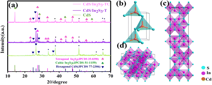 | ||
| Fig. 1 (a) XRD patterns of CdS, CdS/In2S3-T and CdS/In2S3-TC, the crystal structure of hexagonal CdS (b), tetragonal In2S3 (c), cubic In2S3 (d). | ||
Morphology is part of the PEC performance of a photoelectrode and was characterized by SEM. Fig. 2(a) shows that CdS with a smooth surface and about 400 nm particle size is uniformly distributed and grown vertically on the FTO glass surface. When In2S3 was grown on the surface of CdS after the second hydrothermal growth, wedge-shaped In2S3 with a size of about 1.5–2 μm was generated on the surface almost covering the CdS nanorods. On prolonging the reaction time, the size of CdS/In2S3-TC nanoparticles decreased dramatically to about 1 μm. The pore size distribution and BET specific surface area can be obtained by the nitrogen adsorption technique. The BET surface areas were about 0.81 m2 g−1 for CdS and 2.16 m2 g−1 for CdS/In2S3-T, while that of CdS/In2S3-TC significantly increased to 3.55 m2 g−1. The pore distributions were as shown in Fig. S2,† and the pore size of CdS was about 10 nm. The pore size of of CdS/In2S3-T further decreased, while that of CdS/In2S3-TC decreased to around 8 nm. Detailed structural and crystallographic features of CdS/In2S3-TC are represented by TEM and HRTEM (Fig. 2(d–f)). The high-resolution TEM image in Fig. 2(d) shows the successful contact of CdS with In2S3. Fig. 2(e) shows the clear and continuous lattice stripes of the three phases, showing more exposed surfaces, including preferred growth surfaces for the three different phases, with (002) for the hexagonal phase of CdS, (109) for the tetragonal phase of I2S3, and (111) for the cubic phase of In2S3, which is in good agreement with the XRD test results. To further verify the successful attachment of In2S3 with different phase structures to the CdS surface, the contents of elements in CdS/In2S3-TC analyzed by EDS spectroscopic analysis with elemental distribution maps are shown in Fig. 2(f). The three elements In, S, and Cd are successfully and homogeneously distributed in CdS/In2S3-TC.
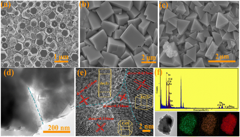 | ||
| Fig. 2 SEM patterns of CdS (a), CdS/In2S3-T (b) and CdS/In2S3-TC (c), TEM of CdS/In2S3-TC (d), HRTEM of CdS/In2S3-TC (e), EDS patterns and mapping images of CdS/In2S3-TC (f). | ||
Any change between atoms leads to a change in bonding energy and a shift in energy levels. Therefore, the effect of phase engineering on the elemental state and energy capture at the electrode material interface was tested by XPS.38 Before analysis, the binding energy was corrected with C 1s (284.8 eV). In addition to the peaks of C and O arising from unconfirmed sources of carbon and oxygen in Fig. 3(a), XPS spectra detected S, Cd, and In, which coincide with the elements studied in this paper. From the high-resolution XPS spectra in Fig. 3(b–d), it can be seen that in CdS/In2S3-T, the 2p3/2 eV and 2p1/2 eV peaks of S were detected at 160.83 eV and 162.03 eV, respectively. The 3d5/2 and 3d3/2 peaks of In were detected at 444.53 eV and 452.08 eV, and the Cd 3d5/2 and Cd 3d3/2 peaks were seen at 405.10 eV and 411.80 eV. Whereas in CdS/In2S3-TC, the 2p3/2 and 2p1/2 peaks appeared at 161.29 eV and 162.54 eV, the 3d5/2 and 3d3/2 peaks of In were detected at 444.83 eV and 452.38 eV, and the peaks of Cd 3d5/2 and Cd 3d3/2 appeared at 405.30 eV and 412.00 eV. It follows that the phase modulation increases the bonding forces between atoms and appears to change the electronic environment. The shielding charge in CdS/In2S3-T reduces the surface crystal potential due to the critical size effect, while CdS/In2S3-TC, which is not a polarized cubic phase, weakens the phenomenon of the disappearance of surface polarity brought about by the surface shielding charge and increases the surface bonding force.
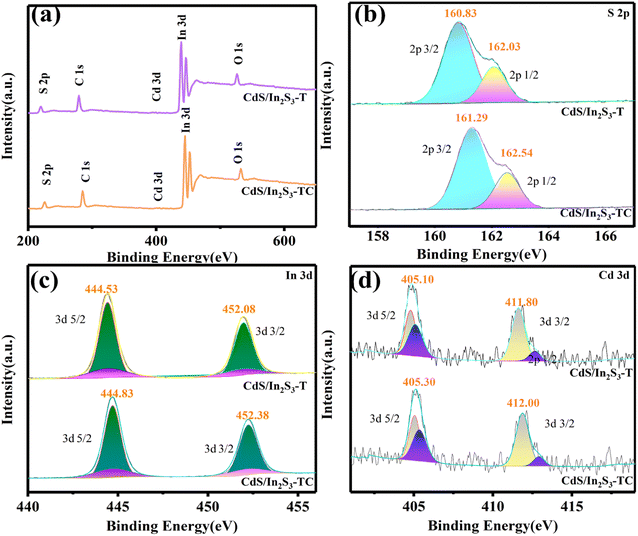 | ||
| Fig. 3 (a) XPS spectra of CdS/In2S3-T and CdS/In2S3-TC, and the related high-resolution spectra of S 2p, Cd 3d and In 3d (b–d). | ||
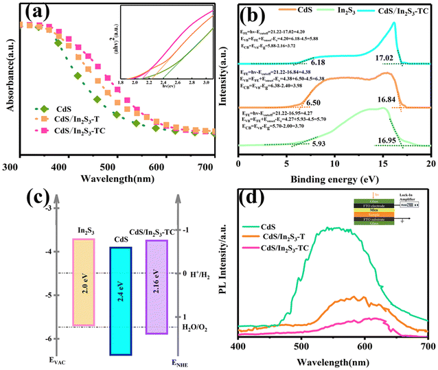
Fig. 4(a) shows the UV-vis absorption spectra of different photoelectrodes used to characterize the absorption capacity of light energy in photoelectrocatalytic systems. The intersection of the tangent line of the curve and the horizontal coordinate is the absorption edge, and the absorption edge of CdS locates at 516 nm, and CdS/In2S3-T locates at 551 nm, indicating that with the formation of the In2S3, the light-absorbing ability increases effectively. In addition, the absorption edge of CdS/In2S3-TC is redshifted, showing a stronger light-absorbing ability, which is having a larger surface area to form a larger light-absorbing surface. The Tauc plots of the samples were calculated from eqn (S1),†39 and the forbidden bandwidth of CdS is at 2.40 eV, which is in agreement with the previous report. The forbidden bandwidth of CdS/In2S3-TC is 2.16 eV, which is reduced by 0.09 eV compared with that of CdS/In2S3-T, which suggests that the composites expose more light-absorbing surfaces to optimize the light-absorbing ability of the semiconductor. The baseband edge positions of the valence band (VB) and conduction band (CB) are determined in conjunction with UPS. Fig. 4(b) shows the cutoff energy (Ecutoff) and onset energy (Eonset) for CdS, In2S3 and CdS/In2S3-TC. According to eqn (S2)–(S4),†40 the position of the ECB and EVB can be calculated. The energy band diagrams of samples based on band gap and UPS are shown in Fig. 4(c) which suggests that the formation of CdS/In2S3 composites with a multi-phase structure enhances the light absorption capacity.41
PL is also another key characterization of light absorption ability. After excitation with a light source of 320 nm, a portion of free carriers will recombine, leading to the process of photoluminescence. The smaller the PL value, the lower the degree of carrier recombination.42Fig. 4(d) shows the PL patterns of different samples. The PL value of CdS reaches the highest value near 540 nm, at which the carrier recombination rate is the largest, and the position of the peak appearance is positively shifted after the complexation of In2S3, which occurs near 580 nm. After the complexation of In2S3, the peak appears positively shifted. It is noteworthy that the intensity of the PL peak of CdS/In2S3-TC decreases, which is related to its large specific surface area and smooth surface, where more active sites are formed on the highly exposed contact surface, while the smooth surface reduces the surface defects and less carriers recombine.
The SPV technique was used to respond to the surface charge nature of the sample, which can indicate the information between the surface charge accumulation of the sample and the wavelength of the incident light, the greater the degree of SPV response, the higher the efficiency of the photogenerated charge separation.24 The positive value of the SPV in Fig. 5(a) indicates that the holes migrate to the surface, and the sample has an n-type property. Photoelectrodes are predominantly electron-conducting and react with oxygen, so this paper focuses on the water oxidation in Pyro-PEC systems of CdS photoelectrodes before and after modification. The CdS/In2S3-T specimen exhibited a strong diffraction peak at 300–500 nm; this is due to the strong light absorption ability of CdS in this region, and a new diffraction peak appears at 500 nm–700 nm, which is due to the strong light absorption ability of In2S3 in this region. It is noteworthy that in CdS/In2S3-TC, a new small diffraction peak appears between 500 and 550 nm, which is caused by the appearance of a new phase within In2S3. The increased intensity of the diffraction peak of CdS/In2S3-TC indicates that more holes are accumulating on the surface, and the holes on the surface of the material are involved in the catalytic chemical reaction, which improves the surface energy.
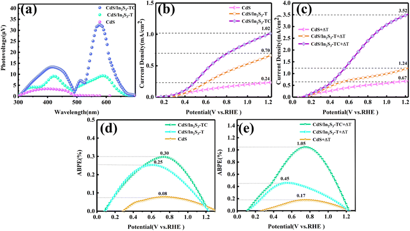 | ||
| Fig. 5 SPV (a), LSV (b), ABPE (d) of different samples under photoelectrocatalytic conditions, LSV (c), ABPE (e) of different samples under pyro-photoelectrocatalytic conditions. | ||
The electrochemical characterization was carried out using a three-electrode electrochemical workstation of model CHI760E with 0.5 M Na2SO4 (pH = 6.8) as the electrolyte, a xenon lamp (Perfect Light, CHF-XM500, 100 mW cm−2) as the external light source, and a water bath as the external drive for the hot–cold cycle. Fig. 5(b and c) shows the linear scanning voltammetry (LSV) curves of the samples at different levels of modification, and the correlation of the potential with the reversible hydrogen electrode (RHE) is calculated by Nernst equation eqn (S5).†43Fig. 5(b) shows the LSV of different samples under photoelectrocatalytic conditions. The current density gradually increases with the increase of the applied bias voltage, and at 1.23 V vs. RHE, the current density is 0.24 mA cm−2 for CdS, 0.70 mA cm−2 for CdS/In2S3-T, and 1.02 mA cm−2, the increase in current density indicates that the formation of CdS/In2S3 can significantly optimize the carrier density of the CdS photoelectrode, and the phase engineering leads to further enhancement of the CdS/In2S3 carrier density. This phenomenon verifies that the enriched phase structure and boundaries have an enhancing effect on the photoelectrode PEC performance. The LSV after the introduction of hot–cold cycling shows a similar trend to that before the introduction, and the current density of CdS/In2S3-TC reaches a maximum value of 3.52 mA cm−2 at 1.23 V vs. RHE. This result verifies that the change of the phase structure affects the internal structure of crystals, which influences the pyroelectric performance of crystals. The LSV curves under photoelectrocatalytic and pyro-photoelectrocatalytic conditions are shown in Fig. S3,† which demonstrate the synergistic effect of pyroelectric and phase engineering on the enhancement of CdS carrier density. The applied bias photon current efficiency (ABPE) was calculated according to eqn (S6)† and the results are shown in Fig. 5(d and e), respectively.44Fig. 5(d) shows that the ABPE values of different samples under photoelectrocatalytic conditions reach a maximum value around 0.8 eV, where CdS/In2S3-TC reaches 0.30%, and when hot–cold cycles are introduced, the maximum value of CdS/In2S3-TC reaches 1.05% in Fig. 5(e), meanwhile, the onset potential decreases. It indicates that phase engineering plays an important role in enhancing the photon conversion to electron capability, and a current response occurs when a small bias voltage is applied. The conversion of CdS/In2S3-TC was further improved after the introduction of a temperature field. The ABPE values of the photoelectrodes before and after modification and temperature field introduction are shown in Fig. S4† indicating that the CdS/In2S3 composites with a rich phase structure and pyroelectric effect played an effective role in enhancing the CdS photoelectrode in the surface oxidation reaction.41
Incident light to current conversion efficiency (IPCE) measurements were used to evaluate the contribution of monochromatic light to the current. The IPCE of various samples at a bias voltage of 1.23 V vs. RHE is shown in Fig. 6 according to eqn (S7),† and the photoelectrode peaks before and after modification all appear near 400 nm, which is consistent with the UV-visible spectral light absorption range. The maximum value of CdS/In2S3-TC reaches 30.24% in Fig. 6(a), which is indicative of the fact that the CdS/In2S3 composites with phase engineering can realize the solar-hydrogen conversion at a longer wavelength range. The PEC performance is significantly enhanced after the introduction of the temperature field. Specifically, the IPCE of CdS/In2S3-T reaches 46.78% and that of CdS/In2S3-TC reaches 55.91% in Fig. 6(b), this is because of the introduction of In2S3 heterophase junctions, where more active sites exist at the heterophase boundary, reducing carrier complexation.45 The IPCE values of the photoelectrodes before and after modification and temperature field introduction are shown in Fig. S5.†
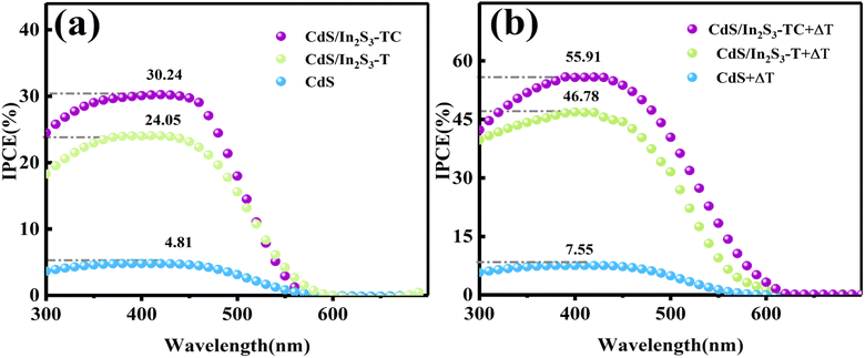 | ||
| Fig. 6 IPCE of different samples under photoelectrocatalytic conditions (a), and pyro-photoelectrocatalytic conditions (b). | ||
Electrochemical impedance spectroscopy (EIS) is commonly used to obtain the charge transfer capacity at the interface between the photoelectrode and the electrolyte, and can be used to characterize the kinetics of charge, which is of great value in PEC systems.46 The EIS curves were tested at −1–1 V vs. Ag/AgCl. The equivalent circuit model is shown in the inset of Fig. 7(a), where Rs is the series resistance, and Ret and CPE are the charge-transfer resistance and constant-phase element at the electrode/electrolyte interface, respectively. The smaller the semicircle, the lower the transfer resistance and the greater the charge transfer capability. Fig. 7(a) shows that the resistance to charge migration is reduced after the formation of CdS/In2S3, and the internal mechanism diagram is shown in Fig. S6.† The formation of a heterojunction led to more active interfaces which established more carrier transport channels and optimized the surface dynamics. Notably, the semicircle of CdS/In2S3-TC becomes smaller, which is related to the formation of the In2S3 heterophase junction, and the presence of active sites for effective charge exchange at the heterophase boundary improves the hole transport efficiency at the photoelectrode/electrolyte interface. The semicircle of CdS/In2S3-TC is minimized after the external temperature field increases the driving force, the pyroelectric effect converts the thermal energy into a built-in electric field, the carrier transfer process obtains a larger driving force, and the atoms at the phase boundaries can be highly activated by the localized charge accumulation, which improves the charge transfer capability.
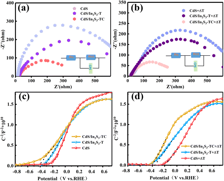 | ||
| Fig. 7 EIS (a) and Mott–Schottky (c) of different samples under photoelectrocatalytic conditions (a), EIS (b) and Mott–Schottky (d) of different samples under pyro-photoelectrocatalytic conditions. | ||
In addition to characterizing the dynamics of carrier migration, Mott–Schottky diagrams at a frequency of 1 kHz under photoelectric and pyro-photoelectrocatalytic conditions were tested as in Fig. 7(c and d) to characterize the carrier density (Nd) and flat band potential (Vfb) according to eqn (S8) and (S9).† The positive slope in the figure indicates that the photoelectrodes have n-type characteristics. Nd and Vfb can be calculated according to the following two equations and the results are shown in Table S1 in the ESI.† The modification strategies decrease the slope, and increase the donor density, and the aggregation of more carriers reduces the energy band bending at the interface and shifts the position of the Fermi energy level upwards. The Schottky barrier is related to the local stress field generated by the polarization electric field, which is excited by the internal polarization electric field of the pyroelectric material when a temperature field is introduced. This is well confirmed by the comparison of Fig. 7(c) and (d), where the flat-band potentials of all types of photoelectrodes are negatively shifted by the temperature field, the built-in electric field strength increases, and the surface state and interfacial barriers decrease. The heterostructure of CdS/In2S3-TC exhibits modulation effects, eliminates space charge defects and optimizes pyroelectricity, which results in more efficient charge transfer.
In order to understand the effect of CdS/In2S3 composites and phase engineering on the pyroelectric properties and the photoelectric performance of the electrode materials, the I–T curves of 1.23 V vs. RHE under different conditions were tested. Fig. 8(a) shows the curve of current density with time under the temperature field of hot–cold cycles, and the ideal temperature variation curve as shown in Fig. 8(b). As can be seen in Fig. 8(a), the current density occurs during both the heating and cooling phases, showing the shape of a cyclic triangle. When the temperature changes, the positions of the atoms in the crystal structure change, and the bound and externally compensated charges are in a state of imbalance, which promotes the oxidation reactions during the process of charge balance. The mechanism is illustrated in Fig. S7.† When the temperature remains constant, there exists an equilibrium between the bound charge and the external compensating charge. However, with an increase in temperature, there is a shift in the position of atoms within the crystal structure, resulting in a decrease in the electric dipole moment and subsequently reducing the number of internal bound charges. Consequently, this leads to a chemical reaction of the electrolyte surrounding the excess compensating charge on the crystal surface. Under constant temperature conditions, the bound charge and the compensating charge remain in equilibrium, causing a consistent decrease in current due to the reduction in both internal and external charges. Conversely, as the temperature decreases, the alteration in the internal polarization field augments the number of bound charges. Simultaneously, compensating charges in the electrolyte migrate towards the material's surface. Consequently, the macroscopic manifestation of temperature change is reflected as an increase in current. The photoelectrodes before and after the modification show a perfect pyroelectric effect. This might be due to the critical size effect, tetragonal phase in the surface of the complex lattice structure and the influence of the external environment. The ferroelectricity at the interface is weakened and affects the polarization strength at the surface. When the partially structured tetragonal phase is transformed into a cubic phase, the transformation of the phase structure at the surface alters the depolarization field strength, which changes the critical size effect on the internal polarized electric field, and CdS/In2S3-TC exhibits superior pyroelectric properties. As can be seen from Fig. 8(c), CdS/In2S3-TC also exhibits better photovoltaic performance, which is related to its greater light response characteristics, as well as an increase in the number of interfaces, which form active sites favorable to the catalyst's performance in the light response properties. Fig. 8(d) shows the I–T curves under pyro-photoelectrocatalytic conditions, and CdS/In2S3-TC still exhibits the best pyro-photoelectrocatalytic performance, and to probe the internal polarization field conditions, we performed PFM tests.
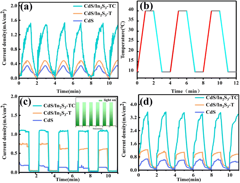 | ||
| Fig. 8 I–T curves under hot–cold cycle (a), ideal temperature change curve (b), I–T curves in the photoelectrocatalytic system (c), and I–T curves in the pyro-photoelectrocatalytic system (d). | ||
The atomic level morphology, electrical domains and phase structure were probed with the PFM light tapping mode, the temperature was raised to 50 °C in an oven before testing.47 The morphology and microscopic domains of the 5 μm × 5 μm photoelectrode are characterized by PFM in Fig. 9. Comparison of the morphology of CdS/In2S3-T and CdS/In2S3-TC (Fig. 9(a and e)) shows that the size of the multiphase structured photoelectrode decreases and the specific surface area increases, which can be well confirmed by the 3D image. In general, the size of the crystal is closely related to the structure of the domains, and as the grain size decreases, the size of the ferroelectric domains decreases as well, which lowers the polarization reversal barriers and promotes polarization reversal, which in turn improves the pyroelectric effect. The amplitude image (Fig. 9(c and g)) clearly shows the morphology of the photoelectrode-rich ferroelectric domains, with the domain walls shown as darker lines, with light and dark representing the polarization strength. During the test, the polarity within the material changes. This is due to the spontaneous polarization modulating the neighboring atomic arrangement and electronic structure, and CdS/In2S3-TC exhibits more pronounced polarization intensity with distinct domain wall boundaries. The domains with polarization vectors on the sample surface correspond to pronounced phase deflections, as can be seen in the phase images (Fig. 9(d and h)), where CdS/In2S3-TC exhibits a more pronounced linear color change and a rich polarization direction. Meanwhile, the ferroelectric hysteresis behavior of the photoelectrode was investigated as shown in Fig. S8,† with a bias voltage between −10 V and 10 V. Clear single hysteresis loops and butterfly-shaped hysteresis loops are observed in the phase and amplitude spectra, respectively, which fully demonstrate that the spontaneous polarization shows ferroelectric switching behavior. Among them, the CdS/In2S3-TC amplitude response shows that the butterfly ring opens at 0.95 V, while the phase also switches 180° at 0.95 V.
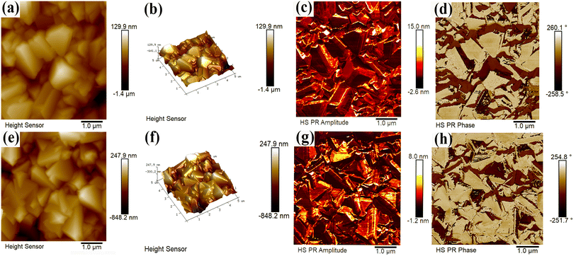 | ||
| Fig. 9 PFM micrographs, 3D image, the relative amplitude image, and phase image of CdS/In2S3-T (a–d) and CdS/In2S3-TC (e–h). | ||
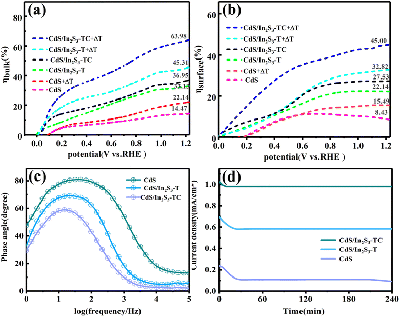
After the separation of electrons and holes, they need to migrate in the bulk and on the surface to participate in the reaction at the active surface, and the transport efficiency is hampered by recombination and resistance in this process.48 To quantitatively characterize the carrier separation efficiency inside the photoelectrode, 0.25 M Na2SO3 was added to 0.5 M Na2SO4 as a cavity scavenger. The charge separation efficiencies were calculated separately for the surface (ηsurface) and bulk (ηbulk) in Fig. 10(a and b), the calculation process is given in eqn (S10).† After adding 0.25 M Na2SO3 as the hole scavenger in 0.5 M Na2SO4, surface recombination of carriers is inhibited, and ηsurface can be considered for 100%. Therefore, in the case of hole scavenger addition, the photocurrent density is decided by eqn (S11),† the ηbulk and ηsurface are calculated by eqn (S12) and (S13).† The ηbulk and ηsurface of CdS at 1.23 V vs. RHE are 8.43% and 14.47%, respectively, with low separation efficiency, indicating severe carrier recombination. After the phase engineering, the carriers can be separated and transferred effectively, and the ηbulk is increased from 14.47% to 36.95%, ηsurface is increased from 8.43% to 22.14%. This is related to the altered electron transfer channel, which lowers the separation barrier. In addition to this, Fig. 10(c) shows the Bode phase diagram of CdS/In2S3-TC. The frequency of peaks in CdS/In2S3-TC is lower than that of the other samples, suggesting that it has a longer carrier lifetime.49 After the introduction of the temperature field, the ηbulk of CdS/In2S3-TC was increased to 63.98% and the ηsurface was increased to 45.00%. This encouraging improvement is extremely important and linked to the enhancement of pyroelectric performance, where the optimization of the internal electric field improves the conductivity of the photoelectrode and reduces the charge recombination improving the charge transfer efficiency, more holes are transferred from the surface of the catalyst to the electrolyte, thus facilitating the reaction.
The stability of photoelectrodes is an important reference performance in the practical application of PEC, for this reason we tested the stability of the samples before and after modification under 240 min of continuous light as shown in Fig. 10(d). The stability of CdS is poor, and the current density of the sample starts to decrease from 0.24 mA cm−2 to 0.11 mA cm−2 after being irradiated by light. When attaching the cubic phase In2S3 to form CdS/In2S3-T, the current density of 0.70 mA cm−2 decreases to 0.60 mA cm−2 and then tends to stabilize. CdS/In2S3-TC was further stabilized, and after 1.5 G of light irradiation, the current density changed slightly and the stability was significantly improved achieving satisfactory results.
The sample after the stability test was characterized in Fig. S9,† some of the particle morphology of CdS/In2S3-T was corroded and the boundaries were dislodged during the reaction process, while the morphology of CdS/In2S3-TC did not undergo obvious change, suggesting that the stability was improved.
Subsequently, the oxygen precipitation capacity of the CdS/In2S3-TC photoelectrode was quantitatively analyzed using gas chromatography, and the Faraday efficiency was calculated according to eqn (S14).†50 Fig. S10† shows that the O2 generation is enhanced after phase engineering modification, and the Faraday efficiencies of CdS/In2S3-T and CdS/In2S3-TC are around 91% and 94%, respectively. The phase engineering reduces the consumption of photogenerated holes by the photoanode, which in turn enhances the stability of the photoelectrode with a higher O2 generation.
4 Conclusion
In conclusion, in this paper, heterogeneous junctions were successfully formed by phase modification engineering, and the feasibility of introducing phase engineering to improve the Pyro-PEC performance of CdS/In2S3 has been demonstrated in this paper. The CdS/In2S3-TC photoanode absorption edge produced by this strategy widens from 516 nm to 575 nm compared to CdS, achieves a charge separation efficiency of 55.91% at 1.23 V vs. RHE, and exhibits a high current density of 3.52 mA cm−2 and further improved stability. The phase-modulated CdS/In2S3 has abundant catalytic active sites at the boundary and active surfaces, which can promote the charge generation and transfer ability to significantly improve the photoelectrical performance. In addition, CdS/In2S3-TC exhibits good field effect modulation, which enhances the spontaneous polarization of the photoelectrode and improves the pyroelectric performance. This study achieves efficient Pyro-PEC water splitting performance by adjusting phase structures on the photoanode, and provides a new idea for the regulation of the polarization electric field.Author contributions
Xingfei Chen, Zhifeng Liu, Mengnan Ruan, Chengyi Wang, and Tingting Zhong conceived and designed the study. Xingfei Chen performed the experiments. Xingfei Chen, Zhifeng Liu, Mengnan Ruan, Chengyi, and Tingting Zhong wrote the paper. Xingfei Chen, Zhifeng Liu, and Mengnan Ruan, reviewed and edited the manuscript. Xingfei Chen, Chengyi, and Tingting Zhong validated the results. All authors read and approved the manuscript.Conflicts of interest
There are no conflicts to declare.Acknowledgements
The authors gratefully acknowledge the financial support from the National Natural Science Foundation of China (No. 52373301 and 52073200).References
- M. H. Khademi, M. Lotfi-Varnoosfaderani and M. H. Moghadasin, Catalytic conversion of bio-renewable glycerol to pure hydrogen and syngas: energy management and mitigation of environmental pollution, Energy Convers. Manage., 2021, 247, 114719 CrossRef CAS.
- M. Jeuland, T. R. Fetter, Y. Li, S. K. Pattanayak, F. Usmani, R. A. Bluffstone, C. Chávez, H. Girardeau, S. Hassen, P. Jagger, M. M. Jaime, M. Karumba, G. Köhlin, L. Lenz, E. L. Litzow, L. Masatsugu, M. A. Naranjo, J. Peters, P. Qin, R. D. Ruhinduka, M. Serrano-TCedrano, M. Sievert, E. O. Sills and M. Toman, Is energy the golden thread? a systematic review of the impacts of modern and traditional energy use in low-and middle-income countries, Renewable Sustainable Energy Rev., 2021, 135, 110406 CrossRef.
- S. Yadav, S. R. Yashas and H. P. Shivaraju, Transitional metal chalcogenide nanostructures for remediation and energy: a review, Environ. Chem. Lett., 2021, 19, 3683–3700 CrossRef CAS.
- T. Zhou, L. Li, J. Li, J. Wang, J. Bai, L. Xia, Q. Xu and B. Zhou, Electrochemically reduced TiO2 photoanode coupled with oxygen vacancy-rich carbon quantum dots for synergistically improving photoelectrochemical performance, Chem. Eng. J., 2021, 425, 131770 CrossRef CAS.
- T. Zhou, S. Chen, L. Li, J. Wang, Y. Zhang, J. Li, J. Bai, L. Xia, Q. Xu, M. Rahim and B. Zhou, Carbon quantum dots modified anatase/rutile TiO2 photoanode with dramatically enhanced photoelectrochemical performance, Appl. Catal., B, 2020, 269, 118776 CrossRef CAS.
- T. Zhou, J. Wang, S. Chen, J. Bai, J. Li, Y. Zhang, L. Li, L. Xia, M. Rahim, Q. Xu and B. Zhou, Bird-nest structured ZnO/TiO2 as a direct Z-scheme photoanode with enhanced light harvesting and carriers kinetics for highly efficient and stable photoelectrochemical water splitting, Appl. Catal., B, 2020, 267, 118599 CrossRef CAS.
- Q. Wang, X. Ma, P. Wu, B. Li, L. Zhang and J. Shi, CoNiFe-LDHs decorated Ta3N5 nanotube array photoanode for remarkably enhanced photoelectrochemical glycerol conversion coupled with hydrogen generation, Nano Energy, 2021, 89, 106326 CrossRef CAS.
- S. Zhang, Z. Liu, D. Chen and W. Yan, An efficient hole transfer pathway on hematite integrated by ultrathin Al2O3 interlayer and novel CuCoOx cocatalyst for efficient photoelectrochemical water oxidation, Appl. Catal., B, 2020, 277, 119197 CrossRef CAS.
- S. He, C. Yan, X. Z. Chen, Z. Wang, T. Ouyang, M. L. Guo and Z. Q. Liu, Construction of core–shell heterojunction regulating α-Fe2O3 layer on CeO2 nanotube arrays enables highly efficient Z-scheme photoelectrocatalysis, Appl. Catal., B, 2020, 276, 119138 CrossRef CAS.
- A. Landman, R. Halabi, P. Dias, H. Dotan, A. Mehlmann, G. E. Shter, M. Halabi, O. Naseraldeen, A. Mendes, G. S. Grader and A. Rothschild, Decoupled photoelectrochemical water splitting system for centralized hydrogen production, Joule, 2020, 4, 448–471 CrossRef CAS.
- S. Yang, H. Guan, Y. Zhong, J. Quan, N. Luo, Q. Gao, Y. Xu, F. Peng, S. Zhang and Y. Fang, CdS@Ni3S2 for efficient and stable photo-assisted electrochemical (P-EC) overall water splitting, Chem. Eng. J., 2020, 405, 126231 CrossRef.
- O. Abdelkarim, J. Kaur, J. Liu, F. Navarro-Pardo, H. Zarrin, A. Yurtsever, G. Bassioni, Z. M. Wang, G. S. Selopal and F. Rosei, Two-dimensional functionalized hexagonal boron nitride for quantum dot photoelectrochemical hydrogen generation, J. Mater. Chem. A, 2020, 8, 20698–20713 RSC.
- T. Zhou, S. Chen, J. Wang, Y. Zhang, J. Li, J. Bai and B. Zhou, Dramatically enhanced solar-driven water splitting of BiVO4 photoanode via strengthening hole transfer and light harvesting by co-modification of CQDs and ultrathin β-FeOOH layers, Chem. Eng. J., 2021, 403, 126350 CrossRef CAS.
- T. Zhou, J. Wang, Y. Zhang, C. Zhou, J. Bai, J. Li and B. Zhou, Oxygen vacancy-abundant carbon quantum dots as superfast hole transport channel for vastly improving surface charge transfer efficiency of BiVO4 photoanode, Chem. Eng. J., 2022, 431, 133414 CrossRef CAS.
- Z. Zhou, J. Chen, Q. Wang, X. Jiang and Y. Shen, Enhanced photoelectrochemical water splitting using a cobalt-sulfide-decorated BiVO4 photoanode, Chin. J. Catal., 2022, 43, 433–441 CrossRef CAS.
- Z. Wang, L. Li, L. Hong, X. Shi, Y. Lu and J. Su, Bi doped Sb2S3 thin film synthesized by a two-step approach with enhanced photoelectrochemical water splitting performance, J. Electrochem. Soc., 2022, 169, 066508 CrossRef CAS.
- L. Wang, W. Lian, B. Liu, H. Lv, Y. Zhang, X. Wu, T. Wang, J. Gong, T. Chen and H. Xu, A transparent, high-performance, and stable Sb2S3 photoanode enabled by heterojunction engineering with conjugated polycarbazole frameworks for unbiased photoelectrochemical overall water splitting devices, Adv. Mater., 2022, 34, 2200723 CrossRef CAS PubMed.
- Y. Lu, Z. Wang and J. Su, Sb2S3 surface modification for improved photoelectrochemical water splitting performance of BiVO4 photoanode, J. Photonics Energy, 2021, 11, 1947–7988 Search PubMed.
- S. Park, J. H. Baek, L. Zhang, J. M. Lee, K. H. Stone, I. S. Cho, J. Guo, H. S. Jung and X. Zheng, Rapid flame-annealed CuFe2O4 as efficient photocathode for photoelectrochemical hydrogen production, ACS Sustain. Chem. Eng., 2019, 5867–5874 CrossRef CAS.
- X. Li, A. Liu, D. Chu, C. Zhang, Y. Du, J. Huang and P. Yang, High performance of manganese porphyrin sensitized p-type CuFe2O4 photocathode for solar water splitting to produce hydrogen in a tandem photoelectrochemical cell, Catalysts, 2018, 8, 108 CrossRef.
- Q. Gao, Z. Jin, L. Qu, Z. Shao, X. Liu, Y. Zhang, Z. Fu, Y. Huang, L. Wang and W. Feng, CuO nanosheets for use in photoelectrochemical photodetectors, ACS Appl. Nano Mater., 2023, 6, 784–791 CrossRef CAS.
- Z. Li, Y. Qu, G. He, M. Humayun, S. Chen and L. Jing, Enhanced visible-light activities for PEC water reduction of CuO nanoplates by coupling with anatase TiO2 and mechanism, Appl. Surf. Sci., 2015, 351, 681–685 CrossRef CAS.
- Y. S. Chaudhary, S. A. Khan, C. Tripathi, R. Shrivastav, V. R. Satsangi and S. Dass, A study on 170 MeV Au13+ irradiated nanostructured metal oxide (Fe2O3 and CuO) thin films for PEC applications, Nucl. Instrum. Methods Phys. Res., Sect. B, 2006, 244, 128–131 CrossRef CAS.
- Y. Li, Q. Wu, Q. Bu, K. Zhang, Y. Lin, D. Wang, X. Zou and T. Xie, An effective CdS/Ti–Fe2O3 heterojunction photoanode: analyzing Z-scheme charge-transfer mechanism for enhanced photoelectrochemical water-oxidation activity, Chin. J. Catal., 2021, 762–771 CrossRef CAS.
- S. Y. Cao, X. Q. Yan, Z. Kang, Q. J. Liang, X. Q. Liao and Z. Yue, Band alignment engineering for improved performance and stability of ZnFe2O4 modified CdS/ZnO nanostructured photoanode for PEC water splitting, Nano Energy, 2016, 24, 25–31 CrossRef CAS.
- S. Wang, X. Zhang, J. Bie, H. Gong, M. Cao, S. Zhang, Y. Jiang, Y. Shen and L. Wang, Influence of Cu doping on physical and photo-electrochemical properties of CdS thin films prepared by RF magnetron sputtering, Mater. Sci. Semicond. Process., 2021, 133, 105933 CrossRef CAS.
- Z. Peng, Y. Su, M. Jafari and M. Siaj, Engineering interfacial band hole extraction on chemical-vapor-deposited MoS2/CdS core–shell heterojunction photoanode: the junction thickness effects on photoelectrochemical performance, J. Mater. Sci. Technol., 2023, 167, 107–118 CrossRef CAS.
- Y. Chen, Y. Wang, X. Zhou, Y. Zhao and W. Peng, Defected graphene as effective co-catalyst of CdS for enhanced photocatalytic activities, Environ. Sci. Pollut. Res., 2020, 27, 26810–26816 CrossRef CAS PubMed.
- J. P. Feser and J. Ravichandran, More power to pyroelectrics, Nat. Mater., 2018, 17, 385–386 CrossRef CAS PubMed.
- A. Trukhin, L. Trinkler and A. Zolotarjovs, Pyroelectric activity of LiGaO2, Li2GeO3, Li2B4O7 and LiNbO3 crystals: pyroelectric luminescence and excitation of cathodoluminescence in scintillator ScPO4, Opt. Mater., 2020, 109, 110391 CrossRef CAS.
- C. Wang, N. Tian, T. Ma, Y. Zhang and H. Huang, Pyroelectric catalysis, Nano Energy, 2020, 78, 105371 CrossRef CAS.
- D. Zhang, H. Wu, C. R. Bowen and Y. Yang, Recent advances in pyroelectric materials and applications, Small, 2021, 17, 2103960 CrossRef CAS PubMed.
- W. Huang, M. Song, Y. Zhang, Y. Zhao, H. Hou, L. H. Hoang and X. Chen, Defects-induced oxidation of two-dimensional β-In2S3 and its optoelectronic properties, Opt. Mater., 2021, 119, 111372 CrossRef CAS.
- S. Pulipaka, A. K. S. Koushik, M. Deepa and P. Meduri, Enhanced photoelectrochemical activity of Co-doped β-In2S3 nanoflakes as photoanodes for water splitting, RSC Adv., 2019, 9, 1335–1340 RSC.
- L. Liu, J. Wu, L. Wu, M. Ye, X. Liu, Q. Wang, S. Hou, P. Lu, L. Sun, J. Zheng, L. Xing, L. Gu, X. Jiang, L. Xie and L. Jiao, Phase-selective synthesis of 1T′ MoS2 monolayers and heterophase bilayers, Nat. Mater., 2018, 17, 1108–1114 CrossRef CAS PubMed.
- Q. Zhao, Z. Liu, Z. Guo, M. Ruan and W. Yan, The collaborative mechanism of surface S-vacancies and piezoelectric polarization for boosting CdS photoelectrochemical performance, Chem. Eng. J., 2022, 433, 133226 CrossRef CAS.
- D. Chen and Z. Liu, Efficient indium sulfide photoelectrode with crystal phase and morphology control for high-performance photoelectrochemical water splitting, ACS Sustain. Chem. Eng., 2018, 6, 12328–12336 CrossRef CAS.
- Z. S. Ma, Y. Wang, Y. L. Huang, Z. F. Zhou, Y. C. Zhou, W. Zheng and C. Q. Sun, XPS quantification of the hetero-junction interface energy, Appl. Surf. Sci., 2013, 265, 71–77 CrossRef CAS.
- B. Zhang, M. Ruan, C. Wang, Z. Guo and Z. Liu, Enhanced photoelectrochemical performance of α-Fe2O3 photoanode modified with NiCo layered double hydroxide, J. Electroanal. Chem., 2023, 936, 117388 CrossRef CAS.
- T. Li, M. Ruan, Z. Guo, C. Wang and Z. Liu, Modulation of Lewis and brønsted acidic sites to enhance the redox ability of Nb2O5 photoanodes for efficient photoelectrochemical performance, ACS Appl. Mater. Interfaces, 2023, 15, 11914–11926 CrossRef CAS PubMed.
- K. Chen, X. M. Zhang, X. F. Yang, M. G. Jiao, Z. Zhou, M. H. Zhang, D. H. Wang and X. H. Bu, Electronic structure of heterojunction MoO2/g-C3N4 catalyst for oxidative desulfurization, Appl. Catal., B, 2018, 238, 263–273 CrossRef CAS.
- Z. Chen, P. Sun, B. Fan, Z. Zhang and X. Fang, In situ template-free ion-exchange process to prepare visible-light-active g-C3N4/NiS hybrid photocatalysts with enhanced hydrogen evolution activity, J. Phys. Chem. C, 2014, 118, 7801–7807 CrossRef CAS.
- H. Cui, T. Wang, Z. Huang, G. Liang, Z. Chen, A. Chen, D. Wang, Q. Yang, H. Hong, J. Fan and C. Zhi, High-voltage organic cathodes for Zinc-ion batteries through electron cloud and solvation structure regulation, Angew. Chem., Int. Ed., 2022, 61, e202203453 CrossRef CAS PubMed.
- A. Ahmad, G. Yerlikaya, Z. Zia-ur-Rehman, H. Paksoy and G. Kardaş, Enhanced photoelectrochemical water splitting using gadolinium doped titanium dioxide nanorod array photoanodes, Int. J. Hydrogen Energy, 2020, 45, 2709–2719 CrossRef CAS.
- E. A. Bondarenko, E. A. Streltsov, M. V. Malashchonak, A. V. Mazanik, A. I. Kulak and E. V. Skorb, Giant incident photon-to-current conversion with photoconductivity gain on nanostructured bismuth oxysulfide photoelectrodes under visible-light illumination, Adv. Mater., 2017, 29, 1702387 CrossRef PubMed.
- M. Zhou, Z. Guo, Q. Song, X. Li and Z. Liu, Improved photoelectrochemical response of CuWO4/BiOI p–n heterojunction embedded with plasmonic Ag nanoparticles, Chem. Eng. J., 2019, 370, 218–227 CrossRef CAS.
- S. Wan, Y. Li, W. Li, X. Mao, W. Zhu and H. Zeng, Room-temperature ferroelectricity and a switchable diode effect in two-dimensional α-In2Se3 thin layers, Nanoscale, 2018, 10, 14885–14892 RSC.
- J. Li, L. Cai, J. Shang, Y. Yu and L. Zhang, Giant enhancement of internal electric field boosting bulk charge separation for photocatalysis, Adv. Mater., 2016, 28, 4059–4064 CrossRef CAS PubMed.
- K. Si, J. Ma, C. Lu, Y. Zhou, C. He, D. Yang, X. Wang and X. Xu, A two-dimensional MoS2/WSe2 van der Waals heterostructure for enhanced photoelectric performance, Appl. Surf. Sci., 2020, 507, 145082 CrossRef CAS.
- L. Guo, P. S. Shinde and Y. Ma, Scalable core–shell MoS2/Sb2Se3 nanorod array photocathodes for enhanced photoelectrochemical water splitting, Sol. RRL, 2020, 4, 1900442 CrossRef CAS.
Footnote |
| † Electronic supplementary information (ESI) available. See DOI: https://doi.org/10.1039/d4ta01455c |
| This journal is © The Royal Society of Chemistry 2024 |

