DOI:
10.1039/D4TA02425G
(Paper)
J. Mater. Chem. A, 2024,
12, 16735-16747
Achieving high overall energy storage performance of KNN-based transparent ceramics by ingenious multiscale designing†
Received
8th April 2024
, Accepted 27th May 2024
First published on 28th May 2024
Abstract
Dielectric capacitors show significant advantages of faster charge–discharge time over solid oxide fuel cells, Li-ion batteries, and electrochemical capacitors and have been considered the best candidates for next-generation high-performance pulsed power systems. Considering the advantage of the feasibility of efficient multifunctional coupling, which meets the integration trend of electronic devices and relies on the excellent transmittance of KNN-based ceramics, we chose KNN-based systems in this work. (1 − x)(K0.5Na0.5)NbO3–xBa0.9Ca0.1Zr0.15Ti0.85O3 ceramics were fabricated by employing conventional solid state technology, and as expected, the substitution of Ba/Ca by K/Na in the A-site and the substitution of Zr/Ti by Nb in the B-site strongly decreased the leakage current of pristine KNN. By multiscale designing, a Wrec of 7.83 J cm−3 with an η of 81.02%, which has huge advantages over both BCZT-based systems and KNN-based systems, was finally achieved when the x equals 0.30, and such an excellent energy storage performance was caused by both high maximum polarization and high large electric breakdown strength. According to their microstructure characterization, the former was caused by the existence of high polarization boundaries induced by the lattice mismatch between the two phases, and the latter was proved by the combined effect of conductive mechanism transition and interface engineering. In addition, relatively high energy storage frequency stability, thermal stability, and polarization fatigue endurance were also obtained, and the charge–discharge behavior indicated their potential in practical applications. The work offered a new concept for designing energy storage capacitors with high overall performance.
1 Introduction
Despite their faster charge–discharge speed over the other three most commonly used battery systems, which are Li-ion batteries, fuel cells, and super-capacitors, energy storage capacitors have been suffering from the drawback of short battery life for quite a long time,1–6 and their development was thus limited. Such a problem is mainly due to the paradox of obtaining large polarization and high electric breakdown strength simultaneously, which have already been reported in many previous studies. Taking the common strategy of domain engineering as an example, based on the physical description in eqn (S1),† refining the domain size for increasing the electric breakdown strength (Eb) indeed works in improving the energy storage density (Wrec) to some extent; the polarization degradation, which happens at the same time, however, shows a negative effect.7–10 A similar issue also exists in studies of film state materials, which always focus on interface engineering. In those cases, artificially introduced interfacial dipole moments strongly improve the total maximum polarization (Pmax) under a high electric field. Nevertheless, the charge accumulation near the interfaces also weakens the voltage endurance for the inevitable increase in ionic conductance.11–14 It is worth noting that compared to film state materials, including both epitaxial thin films and ceramic-polymer hybrid films, bulks store more energy and show more significant potential in applying to large-scale pulsed power equipment; we will thus try to solve the abovementioned paradox to enhance the energy storage capacity of bulk state materials in this work.
Based on the research of the last two decades, the bulk systems for energy storage have been summarized to be bismuth sodium titanate (BNT)-based, strontium titanate (STO)-based, barium titanate–BiMeO3 (BT–BiMeO3)-based, silver niobate (AN)-based, and potassium-sodium niobate (KNN)-based systems.6 Due to the feasibility of efficient multifunctional coupling, which relies on their excellent transmittance and shows huge potential when applied in the military, KNN-based systems have attracted continuous attention from researchers for quite a long time.15,16 KNN-based ceramics' transmittance can also be easily modified by controlling the grain size, crystal structure, density (pores), and domain walls.
But because of the large grain size and volatility of K and Na, pristine KNN suffers from inferior transparency and high leakage current, respectively, and according to what has been reported in the literature, inhibiting the grain growth by obstructing the mass transfer during the sintering process17,18 and heterovalent substitution19 have successfully figured these problems out. Though these two kinds of technologies are pretty mature now, the paradox mentioned above has yet to be solved entirely,20 and the energy storage capacity of KNN-based ceramics still needs to be improved. Modulation within a single degree of freedom seems impossible to satisfy our desire, so the effective solution should lie in a synergistic effect. The Ba1−xCaxZryTi1−yO3 (BCZT) system is a complex solid solution of BaTiO3 (BT), in which the Ca and Zr atoms occupy the A-site and B-site, respectively. It not only has the adjustability of dielectric and ferroelectric properties but also shows the simplicity of obtaining multi-phase structures. The Wrec enhancement in BCZT-based relaxor ferroelectrics has also been successfully achieved via interface-assisted large polarization in our previous work.21 Motivated by this, in this work, we incorporated BCZT into the KNN lattice to form (1 − x)(K0.5Na0.5)NbO3–xBa0.9Ca0.1Zr0.15Ti0.85O3 ((1 − x)KNN–xBCZT) solid solutions. Through multiscale designing: (1) the leakage current was decreased due to the inhibition of electron production; (2) the high polarization boundaries (HPBs), which were induced by the lattice mismatch between the two different phases, were thought to be the reason for the interfacial polarization; (3) the combined effect of the conducting mechanism transition and the interface's blocking effect led to high Eb. Finally, excellent energy storage performances with high energy storage reliability were reached in such transparent ceramics.
2 Experimental section
Details of this part are provided in the ESI.†
3 Results and discussion
3.1 Characterization of the phase and structure
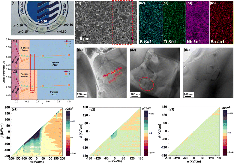
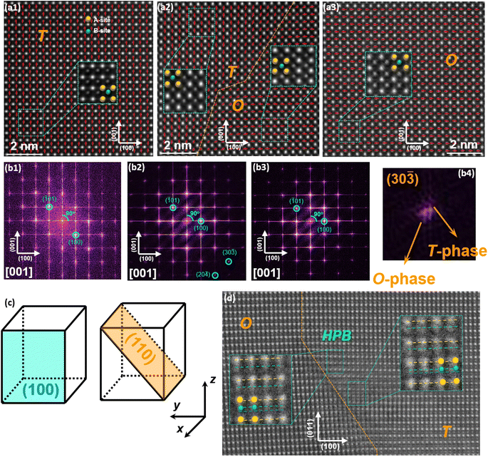
Fig. 1(a) shows the photo of the (1 − x)KNN–xBCZT ceramics with x from 0.10 to 0.50. All of them are transparent, and the one with x = 0.3 has the best transparency (the reason for this will be discussed later). The optical transmittance was also measured and is displayed in Fig. S1(a).†Fig. 1(b1) shows the scanning electron microscope (SEM) image of 0.7KNN–0.3BCZT, and those of (1 − x)KNN–xBCZT with x = 0.1, 0.3, and 0.5 are displayed in Fig. S1(b1)–(b3),† with the grain size distribution in the inset. The average grain size decreases from 1.47 μm to 0.70 μm and then to 0.54 μm, indicating the effect of grain size refinement after the BCZT doping. Fig. 1(b2)–(b5) show the energy disperse spectroscopy (EDS) mappings for K, Ti, Nb, and Ba of the area circled by the red dashed rectangle of Fig. 1(b1), and all of these elements are pretty evenly distributed. Fig. S2† displays the result of the Rietveld XRD refinement of all the (1 − x)KNN–xBCZT ceramics with the corresponding ball–stick models displayed in each figure. The lattice parameters are summarized in Table S1.† The variation between the lattice parameter and the BCZT doping content is plotted in Fig. 1(c1) and (c2). Pure KNN ceramic possesses the orthorhombic phase (O-phase) with the space group of Bmm2, which agrees with a previous report,22 and the ceramic is transferred to the tetragonal phase (T-phase) with the space group of P4mm when the x is 0.1. The two-phase co-existence of the T-phase and O-phase with the space group of P222 was obtained when the x reaches 0.3, and the single structure of P222 is observed in all the remaining components. The Rwp, Rp, and χ2 values, which describe the weighted profile parameter, the unweighted profile parameter, and the goodness of fit of each sample, respectively, are also added in Table S1.† According to their values, such a refinement is highly credible. For more microstructure information, we performed a transmission electron microscopy (TEM) test on (1 − x)KNN–xBCZT ceramics with x = 0.1, 0.3, and 0.5, and the images are displayed in Fig. 1(d1)–(d3). Stripe-like 180° domains were seen in the 0.9KNN–0.1BCZT, as shown in Fig. 1(d1), indicating a large polarization retention.23 Domains with a much smaller size, circled by the red dashed line in Fig. 1(d2), can be observed when the BCZT doping content is increased to 0.3, indicating the transformation from a typical ferroelectric (FE) to a relaxor ferroelectric (RFE).8,24,25 When the BZT doping content is further increased to 0.5, almost no domains can be detected, as seen in Fig. 1(d3), in which case the behavior of a linear dielectric can be predicted. After the microstructure observation, first-order reversal curve (FORC) measurements were also carried out to theoretically analyze the structure–function relationship. By gradually increasing the reversal electric field (β) with a fixed applied electric field (α) of 180 kV cm−1, the diagrams for the FORC distribution were drawn and are displayed in Fig. 1(e1)–(e3). The corresponding waveforms of the ferroelectric hysteresis (P–E) loops are provided in Fig. S3,† and the details of FORC measurements are presented in the Experimental section. As expected, the diagram with the highest-intensity distribution zone in the central region, which results from the large polarization retention, is found in 0.9KNN–0.1BCZT, as mentioned above. For the diagram of 0.7KNN–0.3BCZT, quite a lower polarization retention than the former can be predicted based on its tiny but non-zero, low-intensity distribution zone. The ceramic with a further BZT doping content of 0.5 indicates more even FORC distribution and thus stronger linear dielectric behavior. For more in-depth characterization, the HAADF-STEM images of (1 − x)KNN–xBCZT ceramics with x = 0.1, 0.3, and 0.5 along the [100] crystal axis were recorded. According to the displacement of B-site atoms (weaker contrast) relative to the center of the four adjacent A-site atoms (stronger contrast), the orientation of spontaneous polarization (Ps) of ceramics can be thus confirmed.26,27 0.9KNN–0.1BCZT and 0.5KNN–0.5BCZT show the single T-phase and O-phase with upward and rightward Ps orientation, respectively, as detected in Fig. 2(a1) and (a3). This is consistent with the results of the Rietveld XRD refinement. Similarly, the coexistence of the T-phase and O-phase of 0.7KNN–0.3BCZT can also be confirmed in Fig. 2(a2), and the orange dashed line is the boundary between these two phases, in which the polarization transition region can be seen. Fig. 2(b1)–(b3) show the fast Fourier transform (FFT) images that transformed from Fig. 2(a1)–(a3) using Gwyddion, and the separated patterns indicate the single crystal characteristic of the selected areas for all the ceramics. When zooming in the (30![[3 with combining macron]](https://www.rsc.org/images/entities/char_0033_0304.gif) ) plane of Fig. 2(b2), as shown in Fig. 2(b4), two different patterns, which correspond to the T-phase and O-phase, can be seen, again proving the two-phase coexistence in 0.7KNN–0.3BCZT.
) plane of Fig. 2(b2), as shown in Fig. 2(b4), two different patterns, which correspond to the T-phase and O-phase, can be seen, again proving the two-phase coexistence in 0.7KNN–0.3BCZT.
 |
| | Fig. 1 (a) Picture of (1 − x)KNN–xBCZT ceramics with different x; (b1) SEM image of 0.7KNN–0.3BCZT; (b2)–(b5) EDS mappings for K, Ti, Nb, and Ba of the area circled by the red dashed rectangle in (b1); (c1) and (c2) the variation between the lattice parameter and x; (d1)–(d3) TEM images of (1 − x)KNN–xBCZT ceramics with x = 0.1, 0.3, and 0.5; (e1)–(e3) the FORC distribution of (1 − x)KNN–xBCZT ceramics with x = 0.1, 0.3, and 0.5. | |
 |
| | Fig. 2 (a1)–(a3) The HAADF-STEM images of (1 − x)KNN–xBCZT ceramics with x = 0.1, 0.3, and 0.5 along the [100] crystal axis, and the illustrations in the pictures are the enlarged views of the areas circled by green rectangles; (b1)–(b3) the fast Fourier transform (FFT) images that transformed from (a1)–(a3) using Gwyddion; (b4) enlarged view around the (30) plane of (b2); (c) sketch to show the (100) and (110) planes in the perovskite structure; (d) HAADF-STEM images of the 0.7KNN–0.3BCZT ceramic along the [110] crystal axis, the dislocation can be found between different phases and the B-site atoms near the boundary have relatively large displacement. | |
3.2 Results of the energy storage performance
Before knowing the energy storage performance of the (1 − x)KNN–xBCZT ceramics, the Eb, which is generally obtained via the Weibull distribution of each sample, needs to be calculated, and the details for such a statistical calculation are provided in the ESI.† The result of the Weibull distribution is shown in Fig. 3(a) after measuring 12 different electrodes (each one was considered as one capacitor) in the ceramic of the same component, and the Eb of each ceramic is given in the insert. Finally, the best voltage endurance with an Eb of 604.07 kV cm−1 is found in the (1 − x)KNN–xBCZT ceramic with x = 0.3. The unipolar P–E loops of all these ceramics from 20 kV cm−1 to their Eb are shown in Fig. S4,† and the corresponding Wrec and energy storage efficiency (η) were calculated, and the variation between them and the applied electric field is plotted in Fig. 3(b). To make a comparison within these ceramics, the P–E loops at the Eb of all the ceramics are summarized at the bottom of Fig. 3(c), and on the top, the variation between both Wrec and η and x is also plotted. The highest Wrec of 7.83 J cm−3 with an η of 81.02% was achieved in 0.7KNN–0.3BCZT. To show the advantage of the energy storage performance of our (1 − x)KNN–xBCZT ceramics among the up-to-date BCZT- and KNN-based systems, a comparison diagram, in which the X-axis and Y-axis are Wrec and η, respectively, is illustrated in Fig. 2(d).16,28–56 It can be seen that our ceramics have apparent advantages in energy storage capacity among both systems.
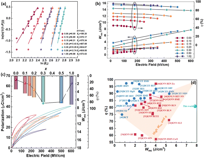 |
| | Fig. 3 (a) Weibull distribution of (1 − x)KNN–xBCZT ceramics and the Eb of each one is shown in the inset; (b) the variation between both Wrec and η and applied electric field; (c) the P–E loops at Eb of all the ceramics are summarized at the bottom, and the Wrec and η of each ceramic are plotted on the top; (d) the comparison between the 0.7KNN–0.3BCZT ceramic in this work and some typical BCZT-based and KNN-based ceramics.16,28–56 | |
3.3 Discussion of the polarization
Fig. 4(a) and (b) show the P–E loops of (1 − x)KNN–xBCZT at 20 kV cm−1 (low field) and 180 (high field) kV cm−1, respectively, and the variations between their Pmax with the difference between them and BCZT doping content are plotted in Fig. 4(c). These results show that the (1 − x)KNN–xBCZT ceramics with lower x show fatter loops and higher Pmax, demonstrating their higher leakage current, and the loop becomes slimmer with increasing x. The higher leakage current can be explained as follows: the lattice-oxygen atoms changed to oxygen and escaped at high sintering temperature, leaving the oxygen vacancies and electrons in the ceramic lattices, as expressed in eqn (1)| |  | (1) |
Because of the volatilization of K and Na in KNN, the following processes happened at the same time.
| |  | (2) |
| |  | (3) |
These two processes consumed electrons and facilitated the reaction of eqn (1);19,57 more electrons were thus produced, resulting in the fat loops and higher Pmax in (1 − x)KNN–xBCZT ceramics with lower x. When BCZT was incorporated into the KNN lattice, Ba/Ca atoms occupied the K/Na sites, and the Nb sites were occupied by Ti/Zr atoms, as sketched in Fig. 4(f1) and (f2). The corresponding defect equations are expressed as follows:
| |  | (4) |
| |  | (5) |
| |  | (6) |
| |  | (7) |
| |  | (8) |
| |  | (9) |
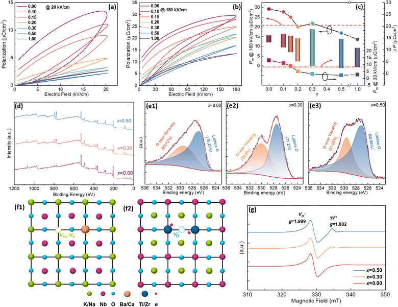 |
| | Fig. 4 The unipolar P–E loops of (1 − x)KNN–xBCZT ceramics under (a) 20 kV cm−1; (b) 180 kV cm−1; (c) the variation between the Pm in (a) and (b) and x with the difference between them; (d) the XPS spectrum from 0–1200 eV; (e1)–(e3) the enlarged XPS spectrum from 524–536 eV; (g) the EPR spectrum of (1 − x)KNN–xBCZT ceramics with x = 0.00, 0.30, and 0.50; (f1) and (f2) sketch of the A-O plane and B-O plane of the lattice of (1 − x)KNN–xBCZT ceramics to explain eqn (1)–(9). | |
The newly formed  inhibited the reactions of eqn (1)–(3) so the number of free electrons was decreased. Here, we have to admit that though the amount of
  with
with  and
and  also increases and the defect dipoles of
  and
and  are thus formed, compared to the free electrons, such defect dipoles have much lower mobility so the leakage current will not increase but decrease. Also, the formation of these defect dipoles decreases the domain, leading to a slimmer P–E loop.58,59 Due to this, the Pmax decreases monotonously with increasing x at 20 kV cm−1. Another proof for such defect equations comes from the electron paramagnetic resonance (EPR) measurement, as seen in Fig. 4(g). The g factor in the spectra is calculated according to eqn (10),
| |  | (10) |
in which ℏ, μB, ν, and B are the Planck constant, Bohr magneton, applied microwave frequency, and resonance magnetic field, respectively. A symmetrical peak around g ∼ 1.999, which indicates the existence of  was observed in the (1 − x)KNN–xBCZT ceramics with x = 0.00, 0.10, and 0.50.60,61 Meanwhile the peak for proving the existence of Ti3+, which is observed around g ∼ 1.982, increases with increasing BCZT doping content. This is because substituting Nb3+ by Ti4+ resulted in extra Ti3+, which agrees well with the above defect equations.62 For the x dependence of Pmax at 180 kV cm−1, with increasing x, the Pmax decreases first from 0 to 0.2, and then an abnormal enhancement can be seen at x = 0.3, and the Pmax decreases again with further increase in doping content. As we have concluded from the results of XRD and TEM, the (1 − x)KNN–xBCZT ceramic with x = 0.3 shows the co-existence of the T-phase and O-phase, and the interfacial polarization might cause such an abnormal enhancement of polarization. To reveal this, we took the HAADF-STEM images of (1 − x)KNN–xBCZT with x = 0.3 along the [110] crystal axis, as displayed in Fig. S5,† and the sketch to show the relative position of (001) and (110) planes is illustrated in Fig. 2(c). The orange line in Fig. S5† represents the phase boundary between the two different phases, and the left area and the right boundary are the O-phase and the T-phase, respectively. Because of the lattice mismatch between the two phases, as we obtained from Table S1,† in which the O-phase has a larger in-plane lattice parameter (a) but a smaller out-of-plane lattice parameter (c) than the T-phase, the lattice distortion can thus be observed. As seen in the enlarged view of area-1, the O-phase side has 13 lattice fringes, while the T-phase side has 12. Similarly, the O-phase side in area-2 has 9 lattice fringes, while the T-phase side has 10. Such an observation verified the results in Table S1.† Then we zoomed in area-3, circled in a red rectangle in Fig. S5,† and displayed it in Fig. 2(d). Because of the lattice mismatch, some B-site atoms in the lattice near the phase boundary have a larger displacement, as circled in the blue rectangles. The yellow and green dashed lines represent the real position of A-site and B-site atoms, respectively, and the blue dashed lines represent the middle position between two yellow lines. Obviously, the B-site atoms in these two areas have large upward displacements, which will lead to high polarization in the 0.7KNN–0.3BCZT ceramic. At this moment, we can almost ensure that the abnormal enhancement of polarization results from these high polarization boundaries (HPBs). Combined with the following equation,
| | | Pi = P − P′ = (εr − εr∞ − εro − 1)ε0E = N(α − α∞ − αo)E | (11) |
which we deduced in the ESI,
† the interfacial polarization is proportional to the applied field, and that is why the abnormal enhancement of polarization is more obvious in the 0.7KNN–0.3BCZT ceramic under 180 kV cm
−1.
3.4 Discussion of the electric breakdown strength with dielectric behaviors
The spheres in Fig. 5(a) show the variation between the Eb obtained from the result of the Weibull distribution (Eb-exp) and the x, and in contrast, the variation between the calculated electric breakdown strength (Eb-cal) and the x is also plotted using smaller squares. The Eb-cal was obtained according to the following equation:| |  | (12) |
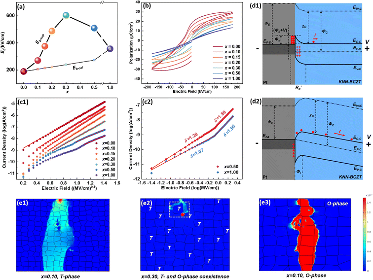 |
| | Fig. 5 (a) The variation between both Eb-exp and Eb-cal and x; (b) bipolar P–E loops of (1 − x)KNN–xBCZT ceramics under 200 kV cm−1; (c1) the fitting result of the J–E curves in Fig. S6† obtained according to (c1) eqn (13); (c2) eqn (14); band diagram to express the (d1) Schottky emission mode and (d2) ohmic contact mode under external bias. (e1)–(e3) The current density distribution of the (1 − x)KNN–xBCZT ceramics with x = 0.10, 0.30, and 0.50 under 550 kV cm−1, respectively. | |
in which Eb-BCZT and Eb-KNN are the experimental Eb of pristine BCZT and KNN ceramics, respectively, and xmax-BCZT and xmax-KNN are the molar ratios of BCZT and BZT parts in each (1 − x)KNN–xBCZT ceramic, respectively. The physical significance of this equation is very simple: it shows how much extra voltage endurance can be obtained by BCZT dissolving into the KNN lattice when compared to the simple linear superposition of the two ceramic components. This figure shows that for simple linear superposition, the electric breakdown strength of (1 − x)KNN–xBCZT ceramics should increase with increasing x. From the experimental result, however, it first increases with increasing x from 0.00 to 0.30 and then decreases with further x increment. Thus, we obviously cannot treat the electric breakdown strength of (1 − x)KNN–xBCZT ceramics as a simple superposition. To reveal the physical mechanism inside, the bipolar P–E loops of all the ceramics were recorded, as shown in Fig. 5(b). Such bipolar loops of (1 − x)KNN–xBCZT ceramics with smaller x have an opening between the starting and ending points, which signifies different ferroelectric behaviors under different voltage directions, and such an opening decreases with increasing x. Considering this, we measured the relationship between the current density and the electric field (J–E curves) of all the ceramics, as plotted in Fig. S6(a).† Then, we fit these J–E curves according to
| |  | (13) |
and
respectively, which are commonly used to determine the Schottky emission mode and the ohmic contact/space charge limited current (SCLC) mode in dielectric films. The J, ΦS, E, T, and σ are the current density, Schottky barrier potential, electric field across the material, absolute temperature, and electrical conductivity, respectively. The A*, k, q, ε0, and εr, which won't change with external factors, are the effective Richardson constant, Boltzmann constant, electronic charge, vacuum dielectric constant, and relative dielectric constant, respectively. In typical Schottky emission mode, the relationship between J and E in eqn (12) should be linear, while for eqn (13), the fitting result of σ equaling 1 and 2 indicates the conduction mechanism of ohmic contact mode and SCLC mode, respectively.63Fig. 5(c1) shows the fitting result of all the (1 − x)KNN–xBCZT ceramics according to eqn (12) obtained by employing Origin 9 software. Although all the curves have a linear part, they deviate with increasing x, especially for 0.5KNN–0.5BCZT and pristine BCZT. Then, we fit the J–E curves of these two components according to eqn (13), and the segmented linear relationship with two different slopes was detected in both. The σ of 0.5KNN–0.5BCZT equals 1.28 and 1.89 under low and high electric fields, respectively, and that of pristine BCZT equals 1.07 and 1.96, respectively, as seen in Fig. 5(c2). The slope change signifies the transition of the conducting mechanism of these two components with increasing applied electric field. Before more discussion on it, which will be provided in the following part, at this moment, we can already provide quite a reasonable explanation of the variation in Fig. 5(a). For (1 − x)KNN–xBCZT ceramics with smaller x, more electrons, which serve as the majority carriers, exist in the matrix and make them show n-type behavior. Additionally, based on the author's previous work and some other literature, the work function of the Pt electrode (ΦE) is 5.56 eV, and the work function of KNN and BCZT is ∼4.06 eV and ∼4.8 eV (close to that of BaTiO3), respectively,64–66 resulting in the work function of (1 − x)KNN–xBCZT ceramics (ΦC) being between them. In this case, the ideal band diagram near the Pt/(1 − x)KNN–xBCZT interface under applied bias can be depicted in Fig. 5(d1). A depletion region (Rd), which contains many trapped electrons, is formed at the interface. When the x is smaller, more electrons exist in the Rd, so its width is broader. Thus, the electrons have higher average mobility, and the ceramics break down more easily. When the x increases, as concluded from eqn (1)–(9), the number of electrons decreases, which makes the Rd thinner and the mobility lower, leading to higher Eb and the increment tendency before x = 0.3 in Fig. 5(a). For (1 − x)KNN–xBCZT ceramics with a larger x of over 0.3, as mentioned above, a deviation happens. This is because the newly formed  as expressed in eqn (1)–(9), increases the electron affinity of the ceramics (χC) and their Fermi level (EF-C) moves down. When the EF-C is lower than the Fermi level of the Pt electrode (EF-E), the conduction mechanism will change from Schottky emission mode to ohmic contact mode, and the corresponding band diagram can be depicted in Fig. 5(d2).67,68 All the applied voltage drops across the ceramic, and there is no depletion region in the Pt/(1 − x)KNN–xBCZT interface anymore, with the loss of the trap effect to the electrons at the same time. Because of this, though the number of free electrons in (1 − x)KNN–xBCZT ceramics decreases monotonously with increasing x, all the electrons in 0.5KNN–0.5BCZT and pristine BCZT are free to move in the whole ceramics, making the electric breakdown easier to happen when under higher electric fields, and finally leading to the decrement tendency after x = 0.3 as shown in Fig. 5(a). As abovementioned, the change of the slope in Fig. 5(c2) means the transition of the conducting mechanism for both 0.5KNN–0.5BCZT and pristine BCZT, and the conducting mechanism transfers from ohmic contact mode to SCLC mode with the electric field increasing. The details of the formation of these two band diagrams are shown in Fig. S7,† and the physical meaning of the abbreviations is also explained in the ESI.† In addition to the above reasons, compared to the other components, (1 − x)KNN–xBCZT ceramics with x = 0.3 show two-phase coexistence, meaning that the interface area between the T-phase and O-phase also helps to increase its voltage endurance, which has already been proven by lots of studies.69–71 Due to these two factors, 0.7KNN–0.3BCZT possesses the highest Eb of 604.07 kV cm−1. To confirm such discussions above, the UV-vis absorption spectra of (1 − x)KNN–xBCZT ceramics with x = 0.1, 0.3, and 0.5 are adopted, and the result is plotted in Fig. S6(b).† By employing the following formula:
where ℏ,
v,
α, and
A are the Planck constant, photon frequency, absorption factor, and a constant, respectively,
72 the band gap (
Eg) of (1 −
x)KNN–
xBCZT with
x = 0.1, 0.3, and 0.5 was fitted to be 3.026 eV, 3.005 eV, and 2.970 eV, respectively, as seen in
Fig. 6(a). For dielectrics, the
Eg is normally positively proportional to their voltage endurance; this result agrees well with the tendency in
Fig. 5(a), proving the correctness of our discussions above.
73 Besides, the reason for the best transparency in ceramics with
x = 0.3, which we have mentioned above, can be revealed at this moment. On one hand, the transparency of polycrystalline ceramics increases with decreasing grain size for the decrement of pores, so the increasing BCZT dopant should improve the transparency of (1 −
x)KNN–
xBCZT ceramics; on the other hand, one of the most fundamental conditions for transparency in ceramics is that the band-gap energy should be higher than 3.26 eV because in this case, the photon does not have sufficient energy to excite the valence electrons.
74–76
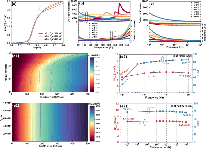 |
| | Fig. 6 (a) The fitting results of Fig. S6† according to eqn (15) to obtain the Eg of (1 − x)KNN–xBCZT with x = 0.1, 0.3, and 0.5; (b) the ε–T curves with tan![[thin space (1/6-em)]](https://www.rsc.org/images/entities/char_2009.gif) δ–T curves of the (1 − x)KNN–xBCZT ceramics from 50 °C to 475 °C at 1000 Hz; (c) the ε–f curves with the tan δ–T curves of the (1 − x)KNN–xBCZT ceramics from 50 °C to 475 °C at 1000 Hz; (c) the ε–f curves with the tan![[thin space (1/6-em)]](https://www.rsc.org/images/entities/char_2009.gif) δ–f curves of the (1 − x)KNN–xBCZT ceramics from 102 to 106 Hz at room temperature; (d1) the mapping to show the variation between polarization and both the applied frequency and the electric field; (d2) the variation between both Wrec and η and frequency; (e1) the mapping to show the variation between polarization and both the cycling number and the electric field; (e2) the variation between both Wrec and η and the cycling number. δ–f curves of the (1 − x)KNN–xBCZT ceramics from 102 to 106 Hz at room temperature; (d1) the mapping to show the variation between polarization and both the applied frequency and the electric field; (d2) the variation between both Wrec and η and frequency; (e1) the mapping to show the variation between polarization and both the cycling number and the electric field; (e2) the variation between both Wrec and η and the cycling number. | |
To visually observe the difference in the electric breakdown behavior of the (1 − x)KNN–xBCZT ceramics with different x under the effect of the conductive mechanism transition and interface engineering, computer simulation was applied using the finite element method through COMSOL Multiphysics 6.0 linked with Matlab 5.2. Fig. 5(e1)–(e3) depict the current density distribution of the (1 − x)KNN–xBCZT ceramics with x = 0.10, 0.30, and 0.50 under 550 kV cm−1, respectively. Based on the result of the Rietveld XRD refinement and the fitting result of the J–E curves, 0.9KNN–0.1BCZT and 0.5KNN–0.5BCZT were set to be a single T-phase and single O-phase, respectively, while 0.7KNN–0.3BCZT was set to be the coexistence of the T-phase and O-phase and the T-phase content was set to be ∼38.32%. Besides, the conduction mode of 0.9KNN–0.1BCZT and 0.7KNN–0.3BCZT was set to be the Schottky emission, while that of 0.5KNN–0.5BCZT was set as ohmic contact. More details on the physical model of such a simulation are explained in the ESI.† From the result, we can see that expect 0.7KNN–0.3BCZT, both the other two components were broken down, and interfaces between the T-phase and O-phase in 0.7KNN–0.3BCZT indeed have blocking behavior to the spread of the current, as marked by the white dashed rectangle. The result of the finite element simulation agrees well with the experimental result. Fig. S8(a1)–(a3) and (b1)–(b3)† display the distribution of the electric potential and electric field of these three ceramics under 550 kV cm−1, respectively. The excellent electric breakdown strength of the 0.7KNN–0.3BCZT ceramic is caused by the combined effect of the conductive mechanism transition and interface engineering.
3.5 Characterization of the energy storage reliability with charge–discharge behavior
Fig. S9† displays the temperature dependence of the dielectric constant (ε–T curve) and dielectric loss (tan![[thin space (1/6-em)]](https://www.rsc.org/images/entities/char_2009.gif) δ–T curve) of all the (1 − x)KNN–xBCZT ceramics from 50 °C to 475 °C at different frequencies, and the curve at 1000 Hz of each component is picked up and summarized in Fig. 6(b). With x increasing, the Curie temperature (Tc) of (1 − x)KNN–xBCZT ceramics shifts to lower temperatures, and the transition peaks start to overlap. Meanwhile, the frequency dispersion, phase transition diffusion, and ε decrement are also observed, manifesting the typical ferroelectric to relaxor ferroelectric (FE-to-RFE) phase transition. Fig. 6(c) plots the frequency dependence of ε (ε–f curve) and tan
δ–T curve) of all the (1 − x)KNN–xBCZT ceramics from 50 °C to 475 °C at different frequencies, and the curve at 1000 Hz of each component is picked up and summarized in Fig. 6(b). With x increasing, the Curie temperature (Tc) of (1 − x)KNN–xBCZT ceramics shifts to lower temperatures, and the transition peaks start to overlap. Meanwhile, the frequency dispersion, phase transition diffusion, and ε decrement are also observed, manifesting the typical ferroelectric to relaxor ferroelectric (FE-to-RFE) phase transition. Fig. 6(c) plots the frequency dependence of ε (ε–f curve) and tan![[thin space (1/6-em)]](https://www.rsc.org/images/entities/char_2009.gif) δ(tan
δ(tan ![[thin space (1/6-em)]](https://www.rsc.org/images/entities/char_2009.gif) δ–f curve) of all the (1 − x)KNN–xBCZT ceramics from 102 Hz to 106 Hz. As a typical FE or RFE, the ε decreases with increasing f, and compared to the other components, 0.7KNN–0.3BCZT shows the best dielectric frequency stability.
δ–f curve) of all the (1 − x)KNN–xBCZT ceramics from 102 Hz to 106 Hz. As a typical FE or RFE, the ε decreases with increasing f, and compared to the other components, 0.7KNN–0.3BCZT shows the best dielectric frequency stability.
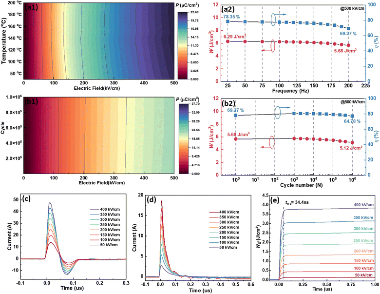
Good dielectric frequency stability would also benefit the energy storage stability. To prove and characterize this, we recorded the unipolar P–E loops of 0.7KNN–0.3BCZT measured from 102 Hz to 104 Hz under 500 kV cm−1 at room temperature. All these loops are shown in Fig. S10(a),† and the variation between polarization and both the applied frequency and the electric field during the voltage ramping up is summarized in a mapping, as displayed in Fig. 6(d1). The polarization increases from the top left to the bottom right. After integration, the variation between the energy storage performance (Wrec and η) and applied frequency is plotted in Fig. 6(d2), and the decrement of Wrec in this whole frequency range is only 21.32%. Energy storage performance after long-term use is also an essential factor in characterizing the reliability of a capacitor, and the unipolar P–E loops of 0.7KNN–0.3BCZT obtained during polarization fatigue from the 1st to the 106th cycle under 500 kV cm−1 are shown in Fig. S10(b).† The mapping of the variation between polarization and both the cycling number and the electric field during the voltage ramping up is displayed in Fig. 6(e1), and the vertical stripes can be clearly seen, which manifest excellent polarization fatigue endurance. Fig. 6(e2) plots the cycling number dependent on the energy storage performance, and the decrement of Wrec is only 2.93%.
To characterize the energy storage thermal stability, the unipolar P–E loops of the 0.7KNN–0.3BCZT ceramic measured from room temperature to 200 °C at 500 kV cm−1 were recorded and are shown in Fig. S11(a),† and the mapping of polarization variation with the electric field and temperature during the voltage ramping up is displayed in Fig. 7(a1). As seen, the polarization measured under the same electric field increases slightly with increasing temperature, and such behavior becomes more obvious at higher electric fields, which is thought to be attributed to the thermally activated dipole polarization.77,78Fig. 7(a2) plots the temperature dependence of the energy storage performance. Both Wrec and η decrease very slowly with increasing temperature, and the decrement is only 9.69% and 11.58%, respectively. Further characterization of reliability is focused on the polarization fatigue endurance in high-temperature environments, so the unipolar P–E loops of the 0.7KNN–0.3BCZT ceramic obtained during polarization fatigue from the 1st to the 106th cycle under 500 kV cm−1 at 200 °C were measured and are shown in Fig. S11(b).† Similar to the fatigue characterization at room temperature, the vertical stripes on the mappings also indicate the polarization fatigue stability at 200 °C under long-term use, as displayed in Fig. 7(b1). After integration, as shown in Fig. 7(b2), the Wrec and η decrement is only 2.93% and 6.48%, respectively.
 |
| | Fig. 7 (a1) The mapping to show the variation between polarization and both temperature and the electric field; (a2) the variation between both Wrec and η and temperature; (b1) the mapping to show the variation between polarization and both the cycling number and the electric field at 200 °C; (b2) the variation between both Wrec and η and the cycling number at 200 °C; the (c) underdamped and (d) overdamped current discharge curves obtained under various electric fields of the 0.7KNN–0.3BCZT ceramic; (e) the time dependence of the WD of the 0.7KNN–0.3BCZT ceramic under different electric fields. | |
The practical application performance of BCZT–0.15BZT as an energy storage capacitor was determined through an R–L–C circuit with a load resistance (RL) of 100 Ω using the pulsed charge–discharge test. The underdamped and overdamped current discharge curves obtained under various electric fields of the 0.7KNN–0.3BCZT ceramic are shown in Fig. 7(c) and (d), respectively, and an apparent complete oscillation can be seen in the former while only a positive peak exists in the latter. For the underdamped circumstance, according to the formulae below:
| |  | (16) |
| |  | (17) |
the electric field dependence of current (Imax), current density (CD), and power density (PD) was obtained and is plotted in Fig. S12.† Their maximum value reaches 47.6 A, 752.6 A cm−2, and 77.7 MW cm−3 at 400 kV cm−1, respectively, as plotted in Fig. S12.† For the overdamped circumstance, using the formula below,
in which R, V, I, and t are the load resistance, sample volume, discharge current, and time, respectively, the time dependence of the discharge energy density (WD) of the 0.7KNN–0.3BCZT ceramic under different electric fields was calculated and is plotted in Fig. 7(e), and the WD values are all lower than the corresponding Wrec when compared with Fig. 3(b). The WD (3.75 J cm−3) calculated here is lower than the value calculated using the static method, which is around ∼6.00 J cm−3, as seen in Fig. 3(b). This is due to the clamping effect on the ferroelectric domains, which has been reported frequently elsewhere.79 The t0.9, which is the time required for dielectric capacitors to release 90% of the total energy stored, was observed to be ∼34.4 ns, indicating that the 0.7KNN–0.3BCZT ceramic is a promising candidate for pulsed power capacitor applications.
4 Conclusions and prospects
(1 − x)KNN–xBCZT transparent ceramics were synthesized through conventional solid-state technology, and the intrinsic high leakage current of pristine KNN ceramic was decreased by the inhibition of the formation of electrons after doping BCZT, which was proved by defect equations. A Wrec of 7.83 J cm−3 with an η of 81.02% was finally achieved in the (1 − x)KNN–xBCZT ceramics with x = 0.30 through multiscale designing, and after the characterization of the structure and properties, analysis of the band diagram, and finite element simulation on COMSOL Multiphysics 6.0, the reason for such a good energy storage performance was revealed to be both large Pmax and high Eb. Specifically, the former was caused by HPBs, which were induced by the lattice mismatch between the T-phase and O-phase and were directly observed from the TEM images; the latter was caused by the combined effect of conductive mechanism transition and interface engineering, which was proved by employing the band diagram and computer simulation. After comparing, our ceramics show quite a huge potential when serving as energy storage capacitors among both BCZT- and KNN-based systems. For reliability characterization, the 0.7KNN–0.3BCZT ceramic shows quite good frequency stability, thermal stability, and polarization fatigue endurance at both room temperature and 200 °C. Besides, good charge–discharge behavior with a t0.9 of ∼34.4 ns was also obtained in the 0.7KNN–0.3BCZT ceramic, demonstrating its potential in practical applications.
Author contributions
Zixiong Sun: conceptualization, methodology, writing-reviewing and editing, supervision, and funding acquisition. Shibo Zhao: data curation. Hongmei Jing: writing-reviewing and editing. Qing Guo: software. Ruyue Gao: data curation. Liming Diwu: data curation. Kang Du: Rietveld XRD refinement. Yongping Pu: funding acquisition and supervision.
Conflicts of interest
The authors declared that they have no conflicts of interest in this work.
Acknowledgements
This work was financed by the National Natural Science Foundation of China (52002234), Open Foundation of Hubei Key Laboratory of Micro-Nanoelectronic Materials and Devices (K202313), Open Foundation of Key Laboratory of Auxiliary Chemistry and Technology for Chemical Industry, Ministry of Education, Shaanxi University of Science and Technology (No. KFKT2021-09), and Shaanxi Collaborative Innovation Center of Industrial Auxiliary Chemistry and Technology.
References
- T. Zhang, H. Sun, C. Yin, Y. H. Jung, S. Min, Y. Zhang, C. Zhang, Q. Chen, K. J. Lee and Q. Chi, Prog. Mater. Sci., 2023, 140, 101207 CrossRef CAS.
- J. Chen, Z. Pei, B. Chai, P. Jiang, L. Ma, L. Zhu and X. Huang, Adv. Mater., 2023, 2308670 CrossRef PubMed.
- X. Wang, F. Yang, K. Yu, B. Zhang, J. Chen, Y. Shi, P. Yang, L. He, H. Li, R. Liu, X. Li, Y. Hu, J. Shang and S. Yin, Adv. Mater. Technol., 2023, 8, 2202044 CrossRef CAS.
- Z. Sun, H. Wei, S. Zhao, Q. Guo, Y. Bai, S. Wang, P. Sun, K. Du, Y. Ning, Y. Tian, X. Zhang, H. Jing, Y. Pu and S. Zhang, J. Mater. Chem. A, 2024, 12, 128–143 RSC.
- Y. Gao, W. Qiao, X. Lou, Z. Song, X. Zhu, L. He, B. Yang, Y. Hu, J. Shao, D. Wang, Z. Chen and S. Zhang, Adv. Mater., 2023, 36, 2310559 CrossRef PubMed.
- Z. Sun, Z. Wang, Y. Tian, G. Wang, W. Wang, M. Yang, X. Wang, F. Zhang and Y. Pu, Adv. Electron. Mater., 2019, 6, 1900698 CrossRef.
- Y. Ning, Y. Pu, C. Wu, Z. Chen, X. Zhang, L. Zhang and B. Wang, J. Eur. Ceram. Soc., 2024, 44, 4831–4833 CrossRef CAS.
- Z. Sun, S. Wang, S. Zhao, H. Wei, G. Shen, Y. Pu and S. Zhang, J. Mater. Chem. C, 2024, 12, 859–867 RSC.
- W. Wang, L. Zhang, Y. Yang, W. Shi, Y. Huang, D. O. Alikin, V. Ya. Shur, Z. Lou, A. Zhang, X. Wei, D. Wang, F. Gao, H. Du and L. Jin, J. Mater. Chem. A, 2023, 11, 2641–2651 RSC.
- F. Yan, G. Ge, J. Qian, J. Lin, C. Chen, Z. Liu and J. Zhai, Small, 2022, 19, 2206125 CrossRef PubMed.
- Z. Sun, Y. Bai, J. Liu, G. Jian, C. Guo, L. Zhang and Y. Pu, J. Alloys Compd., 2022, 909, 164735 CrossRef CAS.
- Z. Sun, C. Ma, M. Liu, J. Cui, L. Lu, J. Lu, X. Lou, L. Jin, H. Wang and C. Jia, Adv. Mater., 2016, 29, 27897340 Search PubMed.
- M. D. Nguyen, Y. A. Birkhölzer, E. P. Houwman, G. Koster and G. Rijnders, Adv. Energy Mater., 2022, 12, 2200517 CrossRef CAS.
- Z. Sun, Y. Bai, H. Jing, T. Hu, K. Du, Q. Guo, T. Ye, C. Ma, M. Liu and Y. Pu, Mater. Horiz., 2024 10.1039/d4mh00322e.
- X. Nie, Y. He, Q. Shi, Y. Liang, L. Wei, P. Liang, X. Chao, G. Hu and Z. Yang, J. Adv. Dielectr., 2023, 13, 2242005 CrossRef CAS.
- Q. Chai, F. Zhang, Q. Zhou, Z. Peng, D. Wu, P. Liang, L. Wei, X. Chao and Z. Yang, Small, 2023, 19, 2207464 CrossRef CAS PubMed.
- X. Ren, L. Jin, Z. Peng, B. Chen, X. Qiao, D. Wu, G. Li, H. Du, Z. Yang and X. Chao, Chem. Eng. J., 2020, 390, 124566 CrossRef CAS.
- M. Zhang, H. Yang, D. Li and Y. Lin, J. Alloys Compd., 2020, 829, 154565 CrossRef CAS.
- J. Lin, G. Ge, K. Zhu, H. Bai, B. Sa, F. Yan, G. Li, C. Shi, J. Zhai, X. Wu and Q. Zhang, Chem. Eng. J., 2022, 444, 136538 CrossRef CAS.
- Z. Cen, X. Wang, Y. Huan and L. Li, J. Am. Ceram. Soc., 2018, 101, 2391–2407 CrossRef CAS.
- Z. Sun, Y. Bai, T. Ouyang, Q. Guo, Y. Ning, J. Liu, H. Wei, K. Du, H. Jing, Y. Tian and Y. Pu, Appl. Phys. Lett., 2023, 122, 263904 CrossRef CAS.
- Y. Peng, Z. Tan, J. An, J. Zhu and Q. Zhang, J. Eur. Ceram. Soc., 2019, 39, 5252–5259 CrossRef CAS.
- D. Zhang, D. Sando, P. Sharma, X. Cheng, F. Ji, V. Govinden, M. Weyland, V. Nagarajan and J. Seidel, Nat. Commun., 2020, 11, 349 CrossRef CAS PubMed.
- Y. Ning, Y. Pu, C. Wu, S. Zhou, L. Zhang, J. Zhang, X. Zhang and Y. Shang, J. Mater. Sci. Technol., 2023, 145, 66 CrossRef CAS.
- W. Wang, L. Zhang, R. Jing, Q. Hu, D. O. Alikin, V. Ya. Shur, X. Wei, G. Liu, Y. Yan and L. Jin, Chem. Eng. J., 2022, 434, 134678 CrossRef CAS.
- H. Pan, S. Lan, S. Xu, Q. Zhang, H. Yao, Y. Liu, F. Meng, E.-J. Guo, L. Gu and D. Yi, Science, 2021, 374, 100 CrossRef CAS PubMed.
- A. K. Yadav, C. T. Nelson, S. L. Hsu, Z. Hong, J. D. Clarkson, C. M. Schlepütz, A. R. Damodaran, P. Shafer, E. Arenholz and L. R. Dedon, Nature, 2016, 530, 198 CrossRef CAS PubMed.
- T. Wang, L. Jin, C. Li, Q. Hu and X. Wei, J. Am. Ceram. Soc., 2014, 98, 559 CrossRef.
- K. Xu, P. Yang, W. Peng, L. Li and J. Alloy, Compd, 2020, 829, 116 Search PubMed.
- D. Han, C. Wang, Z. Zeng, X. Wei, P. Wang, Q. Liu, D. Wang, F. Meng and J. Alloy, Compd, 2020, 902, 163721 CrossRef.
- Z. Chen, Y. Pu, Y. Ning, C. Wu, L. Zhang, X. Zhang and B. Wang, Ceram. Int., 2023, 49, 34520 CrossRef CAS.
- M. Zhou, R. Liang, Z. Zhou and X. Dong, J. Mater. Chem. C, 2018, 6, 8528 RSC.
- A. R. Jayakrishnan, P. V. K. Yadav, J. P. B. Silva and K. C. Sekhar, J. Sci.: Adv. Mater. Devices, 2020, 5, 119 Search PubMed.
- X. Fan, P. Li, J. Du, C. Chen, P. Fu, J. Hao, Z. Xue and W. Li, J. Mater. Sci.: Mater. Electron., 2020, 31, 9974 CrossRef CAS.
- A. Jain, Y. G. Wang and H. Guo, Ceram. Int., 2020, 46, 24333 CrossRef CAS.
- Q. Yuan, G. Li, F. Yao, S. Cheng, Y. Wang, R. Ma, S. Mi, M. Gu, J. Li and H. Wang, Nano Energy, 2018, 52, 203–210 CrossRef CAS.
- V. S. Puli, D. K. Pradhan, B. C. Riggs, D. B. Chrisey and R. S. Katiyar, Integr. Ferroelectr., 2014, 157, 139 CrossRef CAS.
- H. Yang, F. Yan, G. Zhang, Y. Lin, F. Wang and J. Alloy, Compd, 2017, 720, 116 CrossRef CAS.
- A. Jain, Y. Wang, N. Wang and F. Wang, Ceram. Int., 2020, 46, 28800 CrossRef.
- S. N. Norkar, P. Aggarwal and V. K. Deshpande, Curr. Appl. Phys., 2022, 39, 250 Search PubMed.
- C. Shi, F. Yan, G. Ge, Y. Wei, J. Zhai and W. Yao, Chem. Eng. J., 2021, 426, 130800 CrossRef CAS.
- Z. Dai, J. Xie, Z. Chen, S. Zhou, J. Liu, W. Liu, Z. Xi and X. Ren, Chem. Eng. J., 2021, 410, 128341 CrossRef CAS.
- J. Song, F. Yan, J. Lin, G. Ge, C. Shi, J. Qian, Y. Hao, Y. Wei and W. Yao, Chem. Eng. J., 2023, 474, 145754 CrossRef CAS.
- Y. Huan, T. Wei, X. Wang, X. Liu, P. Zhao and X. Wang, Chem. Eng. J., 2021, 425, 129506 CrossRef CAS.
- R. Hu, Y. Lin, M. Zhang, Q. Yuan and H. Yang, Mater. Today Energy, 2022, 30, 101185 CrossRef CAS.
- Q. Chen, T. Gao, R. Lang, Z. Tan, J. Xing and J. Zhu, J. Eur. Ceram. Soc., 2023, 43, 2442–2451 CrossRef CAS.
- M. Zhang, H. Yang, D. Li, L. Ma and Y. Lin, J. Mater. Chem. C, 2020, 8, 8777–8785 RSC.
- B. Qu, H. Du and Z. Yang, J. Mater. Chem. C, 2016, 4, 1795–1803 RSC.
- L. Dong, Z. Dai, J. Hou, C. Liu, R. Dai, Y. Liu, W. Liu and S. Gu, J. Energy Storage, 2023, 74, 109527 CrossRef.
- C. Li, Y. Huan, X. Wang, X. Wang, T. Wang and T. Wei, J. Am. Ceram. Soc., 2022, 105, 6158–6167 CrossRef CAS.
- B. Qu, H. Du and Z. Yang, J. Mater. Chem. C, 2016, 4, 1795–1803 RSC.
- L. Wu, Y. Huan, C. Li, F. Jiang and T. Wei, Ceram. Int., 2023, 49, 22015–22021 CrossRef CAS.
- L. Wu, Y. Huan, X. Wang, C. Li, Y. Luo and T. Wei, J. Mater. Sci., 2022, 57, 15876–15888 CrossRef CAS.
- Z. Yang, F. Gao, H. Du, L. Jin, L. Yan, Q. Hu, Y. Yu, S. Qu, X. Wei, Z. Xu and Y.-J. Wang, Nano Energy, 2019, 58, 768–777 CrossRef CAS.
- B. Qu, H. Du and Z. Yang, J. Mater. Chem. C, 2016, 4, 1795–1803 RSC.
- B. Qu, H. Du, Z. Yang and Q. Liu, J. Am. Ceram. Soc., 2017, 100, 1517–1526 CrossRef CAS.
- Z. Cen, S. Bian, Z. Xu, K. Wang, L. Guo, L. Li and X. Wang, J. Adv. Ceram., 2021, 10, 820–831 CrossRef CAS.
- A. P. Espinosa, L. Ramajo, F. Rubio-Marcos, C. Macchi, A. Somoza and M. Castro, J. Eur. Ceram. Soc., 2021, 41, 1288–1298 CrossRef CAS.
- Y. Guo, K. Kakimoto and H. Ohsato, Jpn. J. Appl. Phys., 2004, 43, 6662 CrossRef CAS.
- G. Wang, J. Zheng, H. Bi, S. Wang, J. Wang, J. Sun, Y. Guo and C. Wang, Scr. Mater., 2019, 162, 28–32 CrossRef CAS.
- L.-B. Xiong, J.-L. Li, B. Yang and Y. Yu, J. Nanomater., 2012, 2012, 9 Search PubMed.
- S. Wang, L. Pan, J.-J. Song, W. Mi, J.-J. Zou, L. Wang and X. Zhang, J. Am. Chem. Soc., 2015, 137, 2975–2983 CrossRef CAS PubMed.
- F.-C. Chiu, Adv. Mater. Sci. Eng., 2014, 2014, 578168 Search PubMed.
- F. Opoku, K. K. Govender, C. G. van Sittert and P. P. Govender, Carbon, 2018, 136, 187–195 CrossRef CAS.
- Z. Sun, S. Huang, W. Zhu, Y. A. Birkhölzer, X. Gao, R. A. Avila, H. Huang, X. Lou, E. P. Houwman, M. D. Nguyen, G. Koster and G. Rijnders, APL Mater., 2023, 11, 101129 CrossRef CAS.
- Z. Sun, E. P. Houwman, S. Wang, M. D. Nguyen, G. Koster and G. Rijnders, J. Alloys Compd., 2024, 981, 173758 CrossRef CAS.
- X. Ding, Y. Zhao, H. Xiao and L. Qiao, Appl. Phys. Lett., 2021, 118, 091601 CrossRef CAS.
- G. Jiang, X. Hu and L. Sun, ACS Appl. Electron. Mater., 2023, 5, 3071–3077 CrossRef CAS.
- Z. Sun, J. Liu, H. Wei, Q. Guo, Y. Bai, S. Zhao, S. Wang, L. Li, Y. Zhang, Y. Tian, X. Zhang, H. Jing, Y. Pu and S. Zhang, J. Mater. Chem. A, 2024, 12, 128–143 RSC.
- P. Wang, X. Wang, G. Li, Y. Li, X. Yao and Z. Pan, Chem. Eng. J., 2022, 433, 133676 CrossRef CAS.
- Y. Ning, Y. Pu, C. Wu, Z. Chen, X. Zhang, L. Zhang and B. Wang, J. Eur. Ceram. Soc., 2024, 44, 4831–4843 CrossRef CAS.
- M. Wang, Y. Lin, Q. Yuan, M. Zhang, Y. Yu, F. Yan and H. Yang, Inorg. Chem. Front., 2023, 10, 4578–4586 RSC.
- L. Wu, Y. Huan, X. Wang, C. Li, Y. Luo and T. Wei, J. Mater. Sci., 2022, 57, 15876–15888 CrossRef CAS.
- S. F. Wang, J. Zhang, D. W. Luo, F. Gu, D. Y. Tang, Z. L. Dong, G. E. B. Tan, W. X. Que, T. S. Zhang, S. Li and L. B. Kong, Prog. Solid State Chem., 2013, 41, 20–54 CrossRef CAS.
- A. M. Tsabit and D.-H. Yoon, J. Korean Ceram. Soc., 2021, 59, 1–24 Search PubMed.
- Z. Xiao, S. Yu, Y. Li, S. Ruan, L. B. Kong, Q. Huang, Z. Huang, K. Zhou, H. Su, Z. Yao, W. Que, Y. Liu, T. Zhang, J. Wang, P. Liu, D. Shen, M. Allix, J. Zhang and D. Tang, Mater. Sci. Eng., R, 2020, 139, 100518 CrossRef.
- B. Li, T. Zheng and J. Wu, ACS Appl. Mater. Interfaces, 2021, 13, 37422–37432 CrossRef CAS PubMed.
- Y. Zhang, X. L. Zhong, M. Vopson, J. B. Wang and Y. C. Zhou, J. Appl. Phys., 2012, 112, 014112 CrossRef.
- L. Yang, X. Kong, F. Li, H. Hao, Z. Cheng, H. Liu, J.-F. Li and S. Zhang, Prog. Mater. Sci., 2019, 102, 72 CrossRef CAS.
Footnotes |
| † Electronic supplementary information (ESI) available. See DOI: https://doi.org/10.1039/d4ta02425g |
| ‡ Z. Sun, S. Zhao, and T. Wang contributed equally to this work. |
|
| This journal is © The Royal Society of Chemistry 2024 |
Click here to see how this site uses Cookies. View our privacy policy here.  *abcde,
Shibo
Zhao‡
a,
Ting
Wang‡
c,
Hongmei
Jing
*f,
Qing
Guo
a,
Ruyue
Gao
a,
Liming
Diwu
a,
Kang
Du
g,
Yongming
Hu
 *b and
Yongping
Pu
*e
![[3 with combining macron]](https://www.rsc.org/images/entities/char_0033_0304.gif) ) plane of Fig. 2(b2), as shown in Fig. 2(b4), two different patterns, which correspond to the T-phase and O-phase, can be seen, again proving the two-phase coexistence in 0.7KNN–0.3BCZT.
) plane of Fig. 2(b2), as shown in Fig. 2(b4), two different patterns, which correspond to the T-phase and O-phase, can be seen, again proving the two-phase coexistence in 0.7KNN–0.3BCZT.


 inhibited the reactions of eqn (1)–(3) so the number of free electrons was decreased. Here, we have to admit that though the amount of
  with
with  and
and  also increases and the defect dipoles of
  and
and  are thus formed, compared to the free electrons, such defect dipoles have much lower mobility so the leakage current will not increase but decrease. Also, the formation of these defect dipoles decreases the domain, leading to a slimmer P–E loop.58,59 Due to this, the Pmax decreases monotonously with increasing x at 20 kV cm−1. Another proof for such defect equations comes from the electron paramagnetic resonance (EPR) measurement, as seen in Fig. 4(g). The g factor in the spectra is calculated according to eqn (10),
 was observed in the (1 − x)KNN–xBCZT ceramics with x = 0.00, 0.10, and 0.50.60,61 Meanwhile the peak for proving the existence of Ti3+, which is observed around g ∼ 1.982, increases with increasing BCZT doping content. This is because substituting Nb3+ by Ti4+ resulted in extra Ti3+, which agrees well with the above defect equations.62 For the x dependence of Pmax at 180 kV cm−1, with increasing x, the Pmax decreases first from 0 to 0.2, and then an abnormal enhancement can be seen at x = 0.3, and the Pmax decreases again with further increase in doping content. As we have concluded from the results of XRD and TEM, the (1 − x)KNN–xBCZT ceramic with x = 0.3 shows the co-existence of the T-phase and O-phase, and the interfacial polarization might cause such an abnormal enhancement of polarization. To reveal this, we took the HAADF-STEM images of (1 − x)KNN–xBCZT with x = 0.3 along the [110] crystal axis, as displayed in Fig. S5,† and the sketch to show the relative position of (001) and (110) planes is illustrated in Fig. 2(c). The orange line in Fig. S5† represents the phase boundary between the two different phases, and the left area and the right boundary are the O-phase and the T-phase, respectively. Because of the lattice mismatch between the two phases, as we obtained from Table S1,† in which the O-phase has a larger in-plane lattice parameter (a) but a smaller out-of-plane lattice parameter (c) than the T-phase, the lattice distortion can thus be observed. As seen in the enlarged view of area-1, the O-phase side has 13 lattice fringes, while the T-phase side has 12. Similarly, the O-phase side in area-2 has 9 lattice fringes, while the T-phase side has 10. Such an observation verified the results in Table S1.† Then we zoomed in area-3, circled in a red rectangle in Fig. S5,† and displayed it in Fig. 2(d). Because of the lattice mismatch, some B-site atoms in the lattice near the phase boundary have a larger displacement, as circled in the blue rectangles. The yellow and green dashed lines represent the real position of A-site and B-site atoms, respectively, and the blue dashed lines represent the middle position between two yellow lines. Obviously, the B-site atoms in these two areas have large upward displacements, which will lead to high polarization in the 0.7KNN–0.3BCZT ceramic. At this moment, we can almost ensure that the abnormal enhancement of polarization results from these high polarization boundaries (HPBs). Combined with the following equation,


 as expressed in eqn (1)–(9), increases the electron affinity of the ceramics (χC) and their Fermi level (EF-C) moves down. When the EF-C is lower than the Fermi level of the Pt electrode (EF-E), the conduction mechanism will change from Schottky emission mode to ohmic contact mode, and the corresponding band diagram can be depicted in Fig. 5(d2).67,68 All the applied voltage drops across the ceramic, and there is no depletion region in the Pt/(1 − x)KNN–xBCZT interface anymore, with the loss of the trap effect to the electrons at the same time. Because of this, though the number of free electrons in (1 − x)KNN–xBCZT ceramics decreases monotonously with increasing x, all the electrons in 0.5KNN–0.5BCZT and pristine BCZT are free to move in the whole ceramics, making the electric breakdown easier to happen when under higher electric fields, and finally leading to the decrement tendency after x = 0.3 as shown in Fig. 5(a). As abovementioned, the change of the slope in Fig. 5(c2) means the transition of the conducting mechanism for both 0.5KNN–0.5BCZT and pristine BCZT, and the conducting mechanism transfers from ohmic contact mode to SCLC mode with the electric field increasing. The details of the formation of these two band diagrams are shown in Fig. S7,† and the physical meaning of the abbreviations is also explained in the ESI.† In addition to the above reasons, compared to the other components, (1 − x)KNN–xBCZT ceramics with x = 0.3 show two-phase coexistence, meaning that the interface area between the T-phase and O-phase also helps to increase its voltage endurance, which has already been proven by lots of studies.69–71 Due to these two factors, 0.7KNN–0.3BCZT possesses the highest Eb of 604.07 kV cm−1. To confirm such discussions above, the UV-vis absorption spectra of (1 − x)KNN–xBCZT ceramics with x = 0.1, 0.3, and 0.5 are adopted, and the result is plotted in Fig. S6(b).† By employing the following formula:
![[thin space (1/6-em)]](https://www.rsc.org/images/entities/char_2009.gif) δ–T curves of the (1 − x)KNN–xBCZT ceramics from 50 °C to 475 °C at 1000 Hz; (c) the ε–f curves with the tan
δ–T curves of the (1 − x)KNN–xBCZT ceramics from 50 °C to 475 °C at 1000 Hz; (c) the ε–f curves with the tan![[thin space (1/6-em)]](https://www.rsc.org/images/entities/char_2009.gif) δ–f curves of the (1 − x)KNN–xBCZT ceramics from 102 to 106 Hz at room temperature; (d1) the mapping to show the variation between polarization and both the applied frequency and the electric field; (d2) the variation between both Wrec and η and frequency; (e1) the mapping to show the variation between polarization and both the cycling number and the electric field; (e2) the variation between both Wrec and η and the cycling number.
δ–f curves of the (1 − x)KNN–xBCZT ceramics from 102 to 106 Hz at room temperature; (d1) the mapping to show the variation between polarization and both the applied frequency and the electric field; (d2) the variation between both Wrec and η and frequency; (e1) the mapping to show the variation between polarization and both the cycling number and the electric field; (e2) the variation between both Wrec and η and the cycling number.![[thin space (1/6-em)]](https://www.rsc.org/images/entities/char_2009.gif) δ–T curve) of all the (1 − x)KNN–xBCZT ceramics from 50 °C to 475 °C at different frequencies, and the curve at 1000 Hz of each component is picked up and summarized in Fig. 6(b). With x increasing, the Curie temperature (Tc) of (1 − x)KNN–xBCZT ceramics shifts to lower temperatures, and the transition peaks start to overlap. Meanwhile, the frequency dispersion, phase transition diffusion, and ε decrement are also observed, manifesting the typical ferroelectric to relaxor ferroelectric (FE-to-RFE) phase transition. Fig. 6(c) plots the frequency dependence of ε (ε–f curve) and tan
δ–T curve) of all the (1 − x)KNN–xBCZT ceramics from 50 °C to 475 °C at different frequencies, and the curve at 1000 Hz of each component is picked up and summarized in Fig. 6(b). With x increasing, the Curie temperature (Tc) of (1 − x)KNN–xBCZT ceramics shifts to lower temperatures, and the transition peaks start to overlap. Meanwhile, the frequency dispersion, phase transition diffusion, and ε decrement are also observed, manifesting the typical ferroelectric to relaxor ferroelectric (FE-to-RFE) phase transition. Fig. 6(c) plots the frequency dependence of ε (ε–f curve) and tan![[thin space (1/6-em)]](https://www.rsc.org/images/entities/char_2009.gif) δ(tan
δ(tan ![[thin space (1/6-em)]](https://www.rsc.org/images/entities/char_2009.gif) δ–f curve) of all the (1 − x)KNN–xBCZT ceramics from 102 Hz to 106 Hz. As a typical FE or RFE, the ε decreases with increasing f, and compared to the other components, 0.7KNN–0.3BCZT shows the best dielectric frequency stability.
δ–f curve) of all the (1 − x)KNN–xBCZT ceramics from 102 Hz to 106 Hz. As a typical FE or RFE, the ε decreases with increasing f, and compared to the other components, 0.7KNN–0.3BCZT shows the best dielectric frequency stability.


