Two-dimensional Janus antimony chalcohalides for efficient energy conversion applications†
Poonam
Chauhan
,
Jaspreet
Singh
and
Ashok
Kumar
 *
*
Department of Physics, Central University of Punjab, VPO Ghudda, Bathinda, 151401, India. E-mail: ashokphy@cup.edu.in
First published on 4th June 2024
Abstract
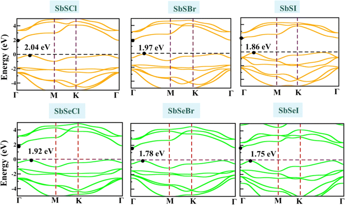
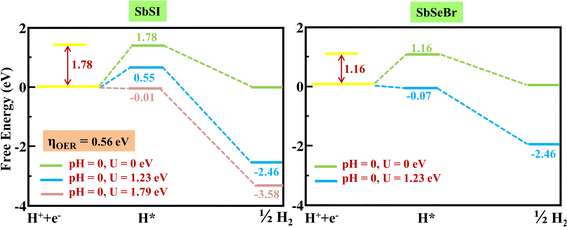
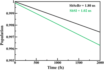
Specific functionalities at the nanoscale can emerge from the broken inversion symmetry in two-dimensional (2D) Janus monolayers. In this work, we employed the first-principles theory to systematically investigate novel 2D Janus SbYZ (Y = S and Se and Z = Cl, Br, and I) monolayers and study their applications in various energy conversion fields such as piezoelectric, thermoelectric, photovoltaic solar cell, and photocatalytic water splitting. The positive phonon spectra and ab initio molecular dynamics (AIMD) simulation plots suggest that these monolayers are dynamically and thermally stable. Our findings demonstrate that these monolayers have extremely low lattice thermal conductivity and excellent electronic transport properties. The computed thermoelectric performances (ZT) of the monolayers range from 0.15 to 1.66 at 800 K. The inspection of the piezoelectric stress and strain coefficients demonstrates strong out-of-plane piezoelectricity. These monolayers also exhibit characteristics such as semiconductor nature, high carrier mobility, and visible light absorption. The proposed heterostructures of these monolayers show high power conversion efficiencies, up to 19% in the case of SbSeBr/AsTeI heterostructures. We have demonstrated the photocatalytic properties of Janus SbSI and SbSeBr monolayers, as the band alignments of these monolayers are appropriate for photocatalytic water splitting. The HER process can occur without an external potential in pH 0 medium for SbSeBr monolayer. The high solar-to-hydrogen (STH) conversion efficiency (up to 18%) and relatively larger electron–hole recombination rates (1.02 ns and 1.80 ns for the Janus SbSI and SbSeBr monolayers, respectively) demonstrated via NAMD simulations indicated that these monolayers are potential materials for efficient photocatalytic water splitting. Our study suggests that these monolayers have the potential for various energy conversion applications.
1. Introduction
After the successful fabrication of single-layer graphene,1 various 2D monolayers were prepared including germanene,2 silicene,3 antimonene,4 and bismuthene.5 Recently, novel 2D material derivatives known as Janus materials have attracted considerable scientific interest due to their distinctive qualities.6 The out-of-plane asymmetry of Janus materials induces an intrinsic electric field (EF).7 The asymmetric nature of Janus monolayers makes them potential candidates for various applications including thermoelectric,8 piezoelectric,9 photovoltaic,10 photocatalytic water splitting,11 and ultrafast charge transfer dynamics in van der Waals heterostructures (vdWHs).12After the successful fabrication of Janus graphene,13 Lu et al. synthesized Janus MoSSe14 and Zheng et al. synthesized Janus WSSe.15 These experimental syntheses led to the theoretical investigations of numerous ternary Janus monolayers based on titanium chalcogenides,16 group-V transition metal trichalcogenides,17 group-IV(A) dichalcogenides,18 antimony-based chalco-halides,19 and transition metal dichalcogenide oxides.20 The thermoelectric properties of 2D Janus monolayers are characterized by a dimensionless quantity called the figure of merit (ZT). A small lattice thermal conductivity and high electrical conductivity are necessary conditions for a high thermoelectric performance. Ternary Janus monolayers such as BiTeBr,21 PdSX (X = Se and Te),22 BiOCl,23 WSX (X = Se and Te),24 AsTeX (Cl, Br and I),25 and BiTeCl (0.43)26 show moderate thermoelectric performance at room temperature (ZT ∼ up to 0.75).
Due to the absence of inversion symmetry, 2D Janus monolayers have an additional degree of freedom to tune piezoelectric properties.27 Piezoelectric materials have broad prospects such as human pulse diagnosis that can measure the weak vibration pattern of the human radial artery28 and detection of pressure distribution.29 The piezoelectric properties of 2D monolayers are characterized by in-plane and out-of-plane piezoelectric coefficients, i.e., d11 and d31. The piezoelectric properties of various Janus monolayers based on bismuth chalcogen halides,30 bismuth oxyhalide,31 group-IV monochalcogenides,9 PtXO (X = S, Se),27 γ-Ge2XX′ (X, X′ = S, Se, and Te),32 SnSSe,33 MoSTe,34 WXO (X = S, Se, and Te),20 X2PAs (X = Si, Ge, and Sn),35 MXY (M = Sb and As; X = Te and Se; Y = Br and I)36 and TiXY (X, Y = Cl, Br, and I)37 have been reported.
Due to the exciting properties of Janus monolayers, researchers further explored their application in excitonic solar cells.38–40 These solar cells feature a type-II band alignment and are centered on the donor–acceptor mechanism between two materials that form a heterostructure.41 Very recently, Janus monolayers were shown to possess good power conversion efficiency (PCE) in photovoltaic solar cells such as Pb2SSe/SnSe (20.02%),42 Pb2SSe/GeSe (19.28%),42 β-Te2S/α-Te2S (21.13%),10 ZrICl (15.91%),43 SbTeBr/SbSI44 and ZrIBr (14.13%).43
Apart from solar cells, Janus structures also show the potential for application in photocatalytic water splitting, which produces clean hydrogen energy using sunlight. For cost-effective commercial application, a photocatalyst's solar-to-hydrogen (STH) conversion efficiency should exceed 10%.45 Various Janus monolayers such as WSSe,46 MoSSe,47 PtSSe,48 WSeTe,49 AsTeX (X = Cl, Br),25 AsXY (X = Se, Te; Y = Br, I),50 and AlXY (X = S, Se; Y = Cl, Br and I)51 possess high STH conversion efficiency. The structural asymmetry-induced intrinsic electric field in Janus monolayers is favourable for hindering charge recombination.46
In addition to various energy conversion applications of 2D materials, the lifetimes of photogenerated charge carriers in these materials play a pivotal role in the performance of energy conversion devices. The suitable carrier lifetimes of 2D monolayers, i.e., black phosphorene (2.4 ns),52 TiO2 (31.1 ns),53 ReS2 (40.1 ps),54 ReSe2 (28.7 ps),54 XMMX′ (X = S, Se; M = Ga, In; X′ = Te) (39.9–72.8 ns),55 LiAlTe2 (1.69 ns),56 PtSe2 (>10 ns),57 MoSi2N4 (489 ps)58 and Cu2O (10.10 ps)59 make them potential candidates for various energy conversion fields.
Inspired by the experimental fabrication of 2D Janus BiTeX (X = Cl, Br and I) compounds,60,61 we systematically explored their analogous novel Janus monolayers SbYZ (Y = S, Se; Z = Cl, Br and I). The dynamical and thermal stability of Janus SbYZ was confirmed by performing phonon and AIMD simulations. We found that 2D SbYZ exhibits very low lattice thermal conductivity with high thermoelectric performance by including various elastic and inelastic scattering mechanisms. Next, we examined the mechanical response and the piezoelectric stress and strain coefficients. The effects of an electric field and magnetic field on free charges were evaluated in terms of Hall conductivity and Hall factor. These monolayers also showed high carrier mobility, computed using Matthiessen's rule, which included various scattering effects, i.e., acoustic, piezoelectric and polar-optical scattering. We also investigated the optical absorption spectrum using the GW+BSE level of theory. Type-II heterojunctions with other monolayers are designed to demonstrate the potential applications of 2D Janus monolayers in solar cells. The high STH conversion efficiency (>10%) with appropriate band edge positions was also obtained for Janus SbSI and SbSeBr monolayers. We also performed ab initio non-adiabatic molecular dynamics (NAMD) simulations on SbSI and SbSeBr Janus monolayers to evaluate the interfacial electron–hole recombination rate and charge transfer dynamics.
2. Computational details
We implemented density functional theory confined in the VASP package62,63 to perform calculations. To describe electron–ion interactions, projected augmented-wave (PAW)64 potentials were employed, while GGA parameterized by PBE65 was implemented to calculate exchange–correlation functionals. To certify the well-founded calculation of electronic properties, the screened hybrid HSE06 method was implemented by mixing nonlocal Fock exchange (25%) with PBE exchange (75%).66 We relaxed the structure until the forces on each atom decreased below 0.01 eV Å−1. The energy convergence criteria between sequential steps for structural relaxation were set to 10−5 eV. For the sampling of the Brillouin zone, the Γ-centred k-mesh of 16 × 16 × 1 (ref. 67) was implemented. A perpendicular cell length of 16 Å was used to eliminate the interactions between the adjoining layers along the z-direction.The phonon dispersion spectra calculations were performed using the DFPT method with a q-mesh of 8 × 8 × 1 and convergence threshold of 10−16 Ry, as incorporated with the Quantum Espresso package.68 The thermal stability of 2D SbYZ Janus monolayers was validated by AIMD simulations at room temperature. To control the temperature in AIMD simulations, the Nose–Hoover thermostat69,70 was employed under the NVT ensemble. The finite difference method confined in VASP was implemented to demonstrate the elastic constants and piezoelectric stress coefficients by integrating the ionic and electronic contributions for the relaxed ions with a 16 × 16 × 1 k-point grid.
The magneto-transport properties were investigated using the theory implemented in the AMMCR package.71 The electrical transport properties calculated by the constant relaxation time approach do not include any scattering mechanisms, which affects the experimental validation of the theoretically anticipated results. Therefore, for more steadiness of theoretically predicted results, we include various kinds of momentum scattering mechanisms as follows:
 | (1) |
The subscripts Ii, Ac, Pz, Dis, Alloy, Iv and Ni in the above equation indicate ionized impurity scattering, polar optical phonon scattering, dislocation scattering, alloy scattering, intra-valley scattering, piezoelectric scattering, acoustic deformation scattering and neutral impurity scattering, respectively.
The lattice transport properties of Janus monolayers were calculated using the Phono3py code.72 The ab initio NAMD simulations were carried out within the Hefei-NAMD code encoded in VASP.73 To obtain charge transfer dynamics, we implemented the (NVT) microcanonical ensemble to perform MD simulation at 300 K with a supercell of size 3 × 3 × 1.
3. Results and discussion
3.1. Geometric structure and energetics
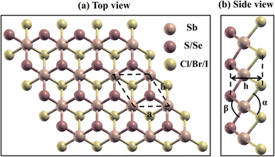
The schematic representation of the geometric optimized structure of 2D Janus SbYZ monolayers is depicted in Fig. 1. Janus SbYZ monolayers exhibit a trigonal structure with a three-atom hexagonal unit cell having a Sb atom sandwiched between Y and Z atoms. These monolayers exhibit a P3m1 space group with a C3v point group. The SbSCl possesses the smallest lattice constant due to the presence of the lightest atoms in it as compared to other SbYZ monolayers. The lattice constant of these monolayers is comparable with previous reports.19,30,36The thickness of Janus monolayers increases with the elongation of bonds, i.e., Sb–Y and Sb–Z, due to the reduction of attractive forces among the layers. On the other hand, the bond angle α (Y–Sb–Y; Y = S, Se and Te) increases while the bond angle β (Z–Sb–Z; Z = Cl, Br and I) shows an opposite trend as given in Table 1. When the electronegativity difference between chalcogen (Y) and halogens (Z) increases, more electrons gather around the more electronegative atoms, which leads to the widening of the bond angle (Table 1).
| 2D monolayer | (a = b) (Å) | h (Å) | α (°) | β (°) | d Sb–Y (Å) | d Sb–Z (Å) | ΔρSb–Y | ΔρSb–Z | ΔΦ (eV) | E C (eV per atom) |
|---|---|---|---|---|---|---|---|---|---|---|
| SbSCl | 3.94 | 3.89 | 86.61 | 94.74 | 2.75 | 2.95 | 0.76 | 0.40 | 0.25 | 3.84 |
| SbSBr | 3.99 | 4.02 | 86.83 | 94.71 | 2.83 | 3.01 | 0.60 | 0.76 | 0.23 | 3.56 |
| SbSI | 4.07 | 4.21 | 87.20 | 94.57 | 2.99 | 3.15 | 0.61 | 0.59 | 0.21 | 3.41 |
| SbSeCl | 4.03 | 3.99 | 88.02 | 97.08 | 3.03 | 3.07 | 0.42 | 0.59 | 0.29 | 3.48 |
| SbSeBr | 4.09 | 4.15 | 88.26 | 97.75 | 3.14 | 3.17 | 0.41 | 0.52 | 0.27 | 3.37 |
| SbSeI | 4.12 | 4.23 | 88.98 | 97.99 | 3.22 | 3.25 | 0.38 | 0.48 | 0.24 | 3.21 |
In Bader charge analysis, ΔρSb–Y (charge transfer from Sb to chalcogens) decreases as the atomic mass corresponding to the chalcogen increases but in the case of ΔρSb–Y (charge transfer from Sb to halogens), an irregular trend is observed. A similar kind of irregular charge transfer behaviour for the case of halogens is observed in the case of MXY (M = Sb, As; X = Te, Se; Y = Br, I)36 and γ-Ge2XX′ (X, X′ = S, Se and Te)32 monolayers. The bond lengths dSb–Y and dSb–Z of SbYZ monolayers increase as the lattice constant “a” increases as we move down the chalcogen and halogen groups. The unbalanced charge between the Y and Z generates an electric field between the Sb-atoms layer and the Y(Z)-atom layer, the direction of which points from Sb to Y(Z). The planar average potential of the SbY/SbZ sides and the potential difference between the two sides, i.e. Y and Z, are also shown in Fig. S1, ESI.† The charge differences between the work function (ΔΦ) of the Y and Z sides are listed in Table 1.
The energetic stability of novel 2D Janus monolayers was quantified in terms of cohesive energy (EC), which is formulated as follows:
 | (2) |
3.2. Dynamical, thermal and mechanical stability
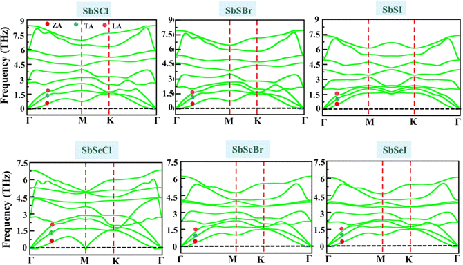
Next, we examine the dynamical and thermal stability of Janus SbYZ monolayers. The dynamical stability of Janus SbYZ monolayers is confirmed by computing phonon dispersion spectra. The phonon dispersion spectra of SbYZ monolayers have no imaginary frequencies, which indicates that these monolayers are dynamically stable, as depicted in Fig. 2. The phonon dispersion spectra of SbYZ monolayers incorporate nine vibrational modes (three acoustic phonon (AP) modes and six optical phonon (OP) modes). Three acoustic phonon modes are characterized by a flexural acoustic (ZA) branch that exhibits quadratic dispersion (p2), a transverse acoustic (TA) branch, and a longitudinal acoustic (LA) branch that possesses linear dispersion near the Γ-point.The phonon modes of SbYZ monolayers shifted to the lower frequencies, and phonon dispersion spectra increased as the atomic mass of constituent atoms increased, as depicted in Fig. 2. In the case of SbSCl, a gap appeared between the AP and OP modes due to the large difference in the atomic masses and the electronegativity differences between the constituent atoms.30 Due to the overlapping of AP and OP modes, strong optical-acoustic scattering arises in SbSBr, SbSI, SbSeCl, SbSeBr and SbSeI. Note that the narrow band dispersion leads to the suppression of their group velocity.32
To confirm the thermal stability of the SbYZ monolayers, we performed AIMD simulations at 300 K (800 K) for 5 ps with a supercell size of 4 × 4 × 1, as shown in Fig. S2, ESI (Fig. S3, ESI†). The variation of temperature with time and the snapshots of final structures show that the crystalline form of Janus SbYZ was maintained at 300 K and 800 K.
After confirming the dynamical and thermal stability, the mechanical stability of the suggested structures was quantified by computing Young's modulus (Y2D), Poisson ratio (ν), and the nonzero elastic constants (Cij), listed in Table 2. All the Janus SbYZ monolayers satisfy the Born and Huang requirements (C11 > |C12| and C66 = (C11 − C12)/2 > 0) for the hexagonal lattice, confirming their mechanical stability.74 The mechanical properties of the 2D SbYZ monolayers were computed by calculating Young's modulus (Y2D) and the Poisson ratio (ν). Young's modulus assesses the stiffness or stretchability of 2D monolayers. The Y2D of 2D Janus SbYZ was computed as follows:
 | (3) |
| 2D monolayers | C 11 (N m−1) | C 12 (N m−1) | Y 2D (N m−1) | (ν) |
|---|---|---|---|---|
| SbSCl | 35.56 | 11.53 | 31.91 | 0.31 |
| SbSBr | 33.83 | 11.96 | 29.60 | 0.34 |
| SbSI | 33.86 | 13.20 | 28.71 | 0.38 |
| SbSeCl | 36.16 | 12.74 | 31.67 | 0.34 |
| SbSeBr | 30.62 | 9.47 | 27.69 | 0.31 |
| SbSeI | 28.07 | 8.05 | 25.76 | 0.28 |
As we move down the halogen group, Y2D decreases, which indicates the elongation of the bonds (dSb–Z). Consequently, SbSeCl and SbSeI yielded the largest and smallest Y2D, respectively. Note that Y2D for SbSeBr was calculated to be 31.14 N m−1 in a previous report.36 Along the stretching direction, the fraction of the transverse strain to the axial strain delivers the Poisson ratio (ν = C12/C11). The computed ν values are in the range of 0.28–0.38, as shown in Table 2. According to the Frantsevich rule,75 the Poisson's ratio of the Janus SbSCl, SbSeBr and SbSeI monolayers are less than 1/3, which implies that these monolayers possess a brittle nature. Note that the Poisson's ratio in previous reports for SbSeBr36 and SbSeI19 was calculated to be 0.32 and 0.23, respectively.
3.3. Piezoelectric properties
The concept of “piezoelectricity” signifies the association of mechanical stress and electrical polarisation that occurs when external stress is applied and induces electric dipole moments in non-centrosymmetric materials, and vice versa. For 2D materials, the z-axis lattice parameter needs to be used to renormalize the piezoelectric stress coefficients, i.e., e11 and e31. Compared to their 3D counterparts, 2D materials exhibit improved piezoelectric constants, according to recent experimental research and theoretical predictions.76 The relaxed-ion piezoelectric tensor (eij) is calculated using a density functional perturbation theory (DFPT) based method, which is formulated as follows:| eij = dikCkj | (4) |
 | (5) |
The relations between piezoelectric coefficients for Janus SbYZ are given as34,77
 | (6) |
The calculated values of piezoelectric coefficients are tabulated in Table 3. The piezoelectric coefficient (d31) of SbSI and SbSeI, is higher as compared to the analogous Janus monolayers such as the MoSSe (0.29 pm V−1),77 MoSTe (0.4 pm V−1),34 1H-WSO (0.4 pm V−1),20 BiSF (−0.33 pm V−1),30 and BiSBr (−0.41 pm V−1)30 monolayers. Such high piezoelectric coefficient values make Janus SbSI and SbSeI monolayers potential candidates for piezoelectric devices. Note that the calculated value of d11 for SbSeBr (21.9 pm V−1) is comparable with the reported value of 22.84 pm V−1 in the literature.36
| 2D monolayers | e 11 (pC m−1) | e 31 (pC m−1) | d 11 (pm V−1) | d 31 (pm V−1) |
|---|---|---|---|---|
| SbSCl | 7.52 | −0.06 | 31.3 | −0.12 |
| SbSBr | 8.16 | −0.11 | 37.3 | −0.26 |
| SbSI | 10.56 | −0.23 | 51.1 | −0.48 |
| SbSeCl | 3.68 | −0.006 | 15.7 | −0.01 |
| SbSeBr | 4.64 | −0.1 | 21.9 | −0.25 |
| SbSeI | 4.16 | −0.22 | 20.8 | −0.60 |
3.4. Thermoelectric properties
| κl,j = ∑∑Cpvg,j2(λ,q′)τ(λ,q′) | (7) |
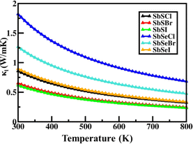
Janus SbYZ monolayers exhibit a decrease in lattice thermal conductivity as temperature increases, indicating Umklapp anharmonic interactions in these monolayers. The calculated values of κl at 300 K range from 0.61 W m−1 K−1 to 1.83 W m−1 K−1 for 2D Janus SbYZ (Fig. 3). The comparison of κl of 2D Janus SbYZ with the other similar monolayer at 300 K is given in Table 4.
| 2D monolayers | κ l (W m−1 K−1) | Reference |
|---|---|---|
| SbSCl, SbSBr, SbSI, SbSeCl, SbSeBr, SbSeI | 0.86, 0.64, 0.61, 1.83, 1.27, 0.91 | This study |
| BiOCl | 3.0 | 78 |
| AsTeCl, AsTeBr, AsTeI | 0.92, 2.02, 3.36 | 25 |
| PdSTe, PdSeTe | 5.45, 4.02 | 22 |
| BiTeCl | 1.46 | 26 |
| BiTeBr | 1.47 | 21 |
| In2SO, In2SeO | 0.42, 0.27 | 8 |
| 1T-ISbTe, 2H-ISbTe | 3.55, 1.63 | 79 |
Next, we computed the phonon's group velocities for different modes as follows:
 | (8) |
κ l can also be expressed in terms of a dimensionless quantity γ as follows:
 | (9) |
γ describes the anharmonic interaction in the crystal structure. A greater value of γ leads to a lower phonon relaxation time due to a higher phonon–phonon scattering rate. The calculated value of γ reached up to ∼45, corresponding to the Janus SbYZ monolayer. The ZA mode in γ contributes more than the TA and LA modes. It was observed that the contribution of optical modes is much less than acoustic modes (Fig. S5, ESI†), which indicates that κl majorly arises due to the anharmonic acoustic scattering of phonons.80 The high value of the Gruneisen parameter and the low value of the group velocity are responsible for the low lattice thermal conductivity in the case of the SbSI monolayer. The higher γ and lower vg are adequate conditions for a monolayer to exhibit low κl.
 | (10) |
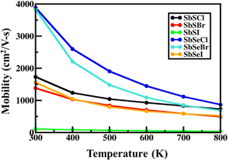
At room temperature, the carrier mobility of SbSeCl and SbSeBr reached 4000 cm2 V−1 s−1. We also studied the effect of magnetic field (B) on charge carriers. The magneto-transport properties of SbYZ monolayers are characterized in terms of the Hall conductivity (σ) and Hall factor (r). The Hall conductivity of SbYZ monolayers is expressed in the form of components of perturbations h(ε) and g(ε). This perturbation arises due to the B. The Hall conductivity in terms of perturbation is given as follows:81
 | (11) |
 | (12) |
We implemented the momentum-dependent scattering mechanism and semi-classical Boltzmann transport theory within the BoltzTraP code for the calculation of electronic transport properties.84 The Seebeck coefficient (S), electronic thermal conductivity (κe), electrical conductivity (σ), and power factor (P) of Janus SbYZ monolayers play an essential role in the calculation of (ZT). The electronic transport parameters, i.e., S, σ and κe are expressed as follows:84
 | (13) |
 | (14) |
 | (15) |
For the computation of κe, we used the Wiedemann–Franz law as follows:
| κe = LσT | (16) |
| PF = S2σ | (17) |
By the integrated effect of κl and PF, the thermoelectric performance of Janus SbYZ monolayers is formulated as follows:86
 | (18) |
The thermoelectric performance gradually increased with temperature (Fig. 6) because of the reduction of the lattice thermal conductivity with temperature. The calculated values of ZT for Janus SbYZ monolayers and their comparison with the other 2D monolayers are listed in Table 5. From this comparison, it is clear that the SbYZ monolayer can act as a potential candidate in the field of thermoelectrics at higher temperatures.
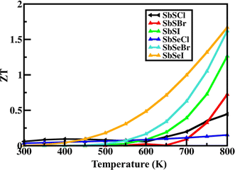 | ||
| Fig. 6 The thermoelectric figure of merit (ZT) of 2D Janus SbYZ monolayers as a function of temperature. | ||
3.5. Optical and photovoltaic solar cell properties
 | (19) |
The optical absorbance spectra of SbYZ monolayers lie in the UV-visible region, with the first most prominent peak being in the visible region, as depicted in Fig. 7. This indicates that these monolayers have excellent visible light harvesting capabilities. The photoexcitation of photogenerated charge carriers is depicted in terms of excitonic binding energy. The excitonic binding energy (Eb) of SbYZ monolayers is as follows:
| Eb = EQP − EOPT | (20) |
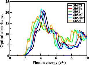 | ||
| Fig. 7 Optical absorbance of 2D Janus SbYZ (Y = S, Se and Z = Cl, Br & I) monolayers using GW-BSE theory. | ||
This excitonic binding energy is lower than other 2D monolayers, i.e., MgO (2.49 eV),89 BeN2 (1.07 eV),90 MoS2 (1.1 eV)91 and β-Te (0.84 eV).92 This signifies that 2D Janus SbYZ monolayers have good potential in the energy conversion fields.
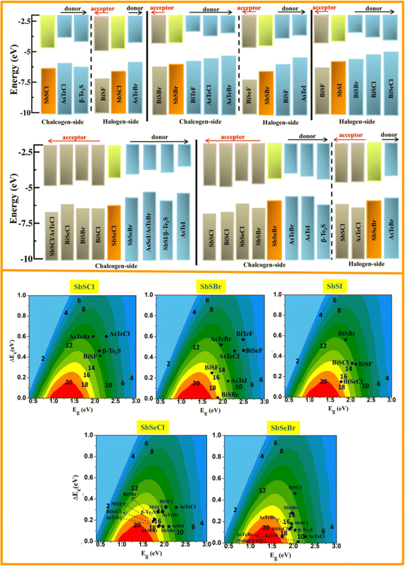
The band alignment of SbYZ monolayers w.r.t. to vacuum level is shown in Fig. 8 (upper panel). We aligned the 2D Janus monolayers corresponding to the chalcogen and halogen sides of SbYZ monolayers with minimum conduction band offset. The appropriate bandgap and smaller ΔEC led to a higher value of PCE. In the case of heterojunction solar cells, the material with the high value of CBM acts as a donor, and other materials act as acceptors.
We implemented the Scharber et al. formula for calculating the power conversion efficiency of the proposed heterostructures.94 PCE can be calculated as follows:
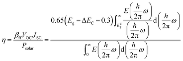 | (21) |
 is the total solar energy. The estimated value of βff is 0.65, which was calculated using the Shockley–Queisser limit. The power conversion efficiency of the proposed heterostructures as a function of donor band gap and conduction band offset is shown in Fig. 8 (lower panel). The PCE value of the Janus SbYZ monolayer and other similar 2D Janus monolayers are tabulated in Table S3, ESI.† The PCE value of SbSeBr/AsTeI heterostructure reached up to 19%, which makes them a potential candidate for photovoltaic solar cells.
3.6. Photocatalytic water-splitting properties
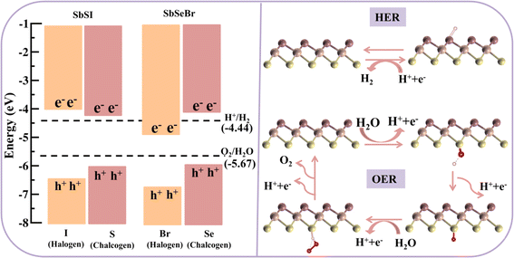
The photocatalytic properties were then computed. Among the different Janus SbYZ monolayers, it was discovered that only SbSI and SbSeBr monolayers had the appropriate band alignments for photocatalytic water splitting. As shown in Fig. 9 (left panel), the valence band position from the halogen side and conduction band position from the chalcogen side properly engulfed the redox potential of water, which made the hydrogen evolution reaction (HER) and oxygen evolution reaction (OER) feasible for both the Janus SbSI and SbSeBr monolayers. The photocatalyst stability in aqueous solution was demonstrated by calculating the reduction and oxidation potentials by implementing the method proposed by Chen and Wang.95 A detailed discussion of the calculation of these potentials is given in the ESI.† | (22) |
η CU is formulated as follows:
 | (23) |
 is as follows:
 | (24) |
The  of the SbSI and SbSeBr monolayers fulfilled the 10% efficiency target for the commercial production of hydrogen. The power conversion efficiencies of SbSI and SbSeBr monolayers and other Janus monolayers are listed in Table S5, ESI.†
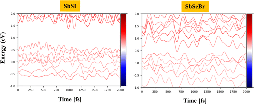 | ||
| Fig. 11 The energy evolution of the Kohn–Sham (KS) states of SbSI and SbSeBr monolayers near the Fermi level at 300 K. | ||
The time-dependent Kohn–Sham orbitals ψx(r,t) are expended in terms of KS orbitals ϕj(r′,R′(t)) as follows:73
 | (25) |
Photon excitation leads to the production of photogenerated charge carriers, electrons (e) and holes (h), in the CBM and VBM, which play a vital role in the recombination process. In the non-radiative electron–hole recombination process, the recombination time of electrons and holes depends on electron–phonon coupling. The recombination rate is determined by non-adiabatic coupling (NAC) and decoherence time.73 The smaller lifetime corresponds to smaller nonadiabatic coupling. The non-adiabatic coupling and decoherence time are related to phonon excitation and electron–phonon coupling. The NAC is given as follows:
 | (26) |
 | (27) |
The calculated values of the electron (hole) transfer rate for SbSI and SbSeBr monolayers are 0.08 ps (11.73 ps) and 5.66 ps (20.96 ps) (Fig. S10, ESI†). The values of τ for the SbSI and SbSeBr monolayers were calculated as 1.02 ns and 1.80 ns, respectively (Fig. 12), which are higher as compared to the other monolayers such as pristine black phosphorene (0.29 ns),52 TiO2 (31.1 ns),53 GaSe (48.6 ns),55 GaS (39.9 ns),55 Ga2SeTe (51.5 ns),55 In2SeTe (61.1 ns),55 In2STe (72.8 ns),55 and PtSe2 (>10 ns).57
4. Conclusions
In this work, we investigated the thermoelectric, piezoelectric, magneto-transport, optoelectronic, photocatalytic, photovoltaic and charge transfer dynamics properties of Janus SbYZ monolayers. The phonon spectra, AIMD simulations and elastic tensor analysis confirmed their dynamical, thermal, and mechanical stability. These monolayers possess low lattice thermal conductivity ranging from 0.61 to 1.83 W m−1 K−1. We incorporated various kinds of elastic and inelastic scattering mechanisms to deal with the electronic transport properties. By the integrated effect of lattice thermal conductivity and electronic transport properties, the computed values of the thermoelectric performance (ZT) of Janus SbYZ monolayers can reach up to ∼1.6 at 800 K. The piezoelectric coefficients were calculated and a large out-of-plane piezoelectric constant was observed in these monolayers. The carrier mobility of these monolayers was calculated using Matthiessen's rule, including the effect of acoustic, piezoelectric and polar-optical scattering; the SbSeCl monolayer carrier mobility reached 4000 cm2 V−1 s−1. To demonstrate the effects of an electric field and magnetic field on free charges, we studied the magneto-transport properties of Janus SbYZ monolayers and these properties were characterized in terms of the Hall conductivity (σ) and Hall factor (r). The most prominent peak of the optical absorbance spectra of SbXY monolayers lies in the visible region. The proposed type-II heterojunction solar cells based on Janus SbYZ monolayers possess high power conversion efficiencies (PCEs), especially in the case of the SbSeBr/AsTeI heterostructures marked up to ∼19%. We also looked into the photocatalytic capabilities of Janus SbSI and SbSeBr monolayers; the redox potential of water lies in the band edge alignment w.r.t to the different surface vacuum potentials of these monolayers. At zero pH, SbSeBr monolayer can be potential candidates for hydrogen generation. Janus SbSI and SbSeBr monolayers showed 12% and 18% STH conversion efficiency, respectively. The charge transfer dynamics properties were studied in the context of photocatalytic water splitting. The calculated prolonged electron–hole recombination rates of SbSI and SbSeBr monolayers were calculated as 1.02 ns and 1.82 ns, respectively. Our study indicates that these monolayers can act as efficient contenders for various energy harvesting fields.Conflicts of interest
There are no conflicts to declare.Acknowledgements
PC & JS thanks the CSIR for providing financial support in the form of a senior research fellowship (SRF). The results presented in this work were obtained using the computational resources at the Department of Physics at the Central University of Punjab.References
- K. S. Novoselov, A. K. Geim, S. V. Morozov, D.-e. Jiang, Y. Zhang, S. V. Dubonos, I. V. Grigorieva and A. A. Firsov, Science, 2004, 306, 666–669 CrossRef CAS PubMed.
- M. Dávila, L. Xian, S. Cahangirov, A. Rubio and G. Le Lay, New J. Phys., 2014, 16, 095002 CrossRef.
- P. Vogt, P. De Padova, C. Quaresima, J. Avila, E. Frantzeskakis, M. C. Asensio, A. Resta, B. Ealet and G. Le Lay, Phys. Rev. Lett., 2012, 108, 155501 CrossRef PubMed.
- E. Martínez-Periñán, M. P. Down, C. Gibaja, E. Lorenzo, F. Zamora and C. E. Banks, Adv. Energy Mater., 2018, 8, 1702606 CrossRef.
- F. Reis, G. Li, L. Dudy, M. Bauernfeind, S. Glass, W. Hanke, R. Thomale, J. Schäfer and R. Claessen, Science, 2017, 357, 287–290 CrossRef CAS PubMed.
- L. Zhang, Z. Yang, T. Gong, R. Pan, H. Wang, Z. Guo, H. Zhang and X. Fu, J. Mater. Chem. A, 2020, 8, 8813–8830 RSC.
- J. Zhang, S. Jia, I. Kholmanov, L. Dong, D. Er, W. Chen, H. Guo, Z. Jin, V. B. Shenoy and L. Shi, ACS Nano, 2017, 11, 8192–8198 CrossRef CAS PubMed.
- T. V. Vu, C. V. Nguyen, H. V. Phuc, A. Lavrentyev, O. Khyzhun, N. V. Hieu, M. Obeid, D. Rai, H. D. Tong and N. N. Hieu, Phys. Rev. B, 2021, 103, 085422 CrossRef CAS.
- N. Ghobadi, S. G. Rudi and S. Soleimani-Amiri, Phys. Rev. B, 2023, 107, 075443 CrossRef CAS.
- J. Singh and A. Kumar, J. Mater. Chem. C, 2023, 11, 1173–1183 RSC.
- D. Ozbey, M. Kilic and E. Durgun, Phys. Rev. Appl., 2022, 17, 034043 CrossRef CAS.
- B. Cai, J. Tan, L. Zhang, D. Xu, J. Dong and G. Ouyang, Phys. Rev. B, 2023, 108, 045416 CrossRef CAS.
- L. Zhang, J. Yu, M. Yang, Q. Xie, H. Peng and Z. Liu, Nat. Commun., 2013, 4, 1443 CrossRef PubMed.
- A.-Y. Lu, H. Zhu, J. Xiao, C.-P. Chuu, Y. Han, M.-H. Chiu, C.-C. Cheng, C.-W. Yang, K.-H. Wei and Y. Yang, Nat. Nanotechnol., 2017, 12, 744–749 CrossRef CAS PubMed.
- B. Zheng, C. Ma, D. Li, J. Lan, Z. Zhang, X. Sun, W. Zheng, T. Yang, C. Zhu and G. Ouyang, J. Am. Chem. Soc., 2018, 140, 11193–11197 CrossRef CAS PubMed.
- Y. Wang, W. Wei, H. Wang, N. Mao, F. Li, B. Huang and Y. Dai, J. Phys. Chem. Lett., 2019, 10, 7426–7432 CrossRef CAS PubMed.
- R. Ahammed, N. Jena, A. Rawat, M. K. Mohanta, Dimple and A. De Sarkar, J. Phys. Chem. C, 2020, 124, 21250–21260 CrossRef CAS.
- P. Nandi, A. Rawat, R. Ahammed, N. Jena and A. De Sarkar, Nanoscale, 2021, 13, 5460–5478 RSC.
- A. Bafekry, M. Faraji, M. Fadlallah, D. Hoat, H. Jappor, I. A. Sarsari, M. Ghergherehchi and S. Feghhi, Phys. Chem. Chem. Phys., 2021, 23, 25866–25876 RSC.
- M. J. Varjovi, M. Yagmurcukardes, F. M. Peeters and E. Durgun, Phys. Rev. B, 2021, 103, 195438 CrossRef CAS.
- S.-D. Guo and H.-C. Li, Comput. Mater. Sci., 2017, 139, 361–367 CrossRef CAS.
- W.-L. Tao, J.-Q. Lan, C.-E. Hu, Y. Cheng, J. Zhu and H.-Y. Geng, J. Appl. Phys., 2020, 127, 035101 CrossRef CAS.
- C.-W. Wu, X. Ren, G. Xie, W.-X. Zhou, G. Zhang and K.-Q. Chen, Phys. Rev. Appl., 2022, 18, 014053 CrossRef CAS.
- A. Patel, D. Singh, Y. Sonvane, P. Thakor and R. Ahuja, ACS Appl. Mater. Interfaces, 2020, 12, 46212–46219 CrossRef CAS PubMed.
- P. Chauhan, J. Singh and A. Kumar, J. Mater. Chem. A, 2023, 11, 10413–10424 RSC.
- P. Chauhan, J. Singh and A. Kumar, J. Phys. Chem. Solids, 2022, 167, 110758 CrossRef CAS.
- W. Zhang and W. Ji, Phys. Rev. B, 2023, 108, 035411 CrossRef CAS.
- Y. Chu, J. Zhong, H. Liu, Y. Ma, N. Liu, Y. Song, J. Liang, Z. Shao, Y. Sun and Y. Dong, Adv. Funct. Mater., 2018, 28, 1803413 CrossRef.
- Y. Cheng, Y. Ma, L. Li, M. Zhu, Y. Yue, W. Liu, L. Wang, S. Jia, C. Li and T. Qi, ACS Nano, 2020, 14, 2145–2155 CrossRef CAS PubMed.
- M. J. Varjovi and E. Durgun, Phys. Rev. Mater., 2021, 5, 104001 CrossRef CAS.
- X. Li, J. Qiu, X. Chen, F. Zhang, Z. Chen and J. Yu, Mater. Lett., 2022, 325, 132867 CrossRef CAS.
- M. J. Varjovi, S. Ershadrad and B. Sanyal, Phys. Rev. B, 2023, 107, 195421 CrossRef CAS.
- S.-D. Guo, X.-S. Guo, R.-Y. Han and Y. Deng, Phys. Chem. Chem. Phys., 2019, 21, 24620–24628 RSC.
- M. Yagmurcukardes, C. Sevik and F. Peeters, Phys. Rev. B, 2019, 100, 045415 CrossRef CAS.
- Y. Wu, C.-H. Yang, H.-N. Zhang, L.-H. Zhu, X.-Y. Wang, Y.-Q. Li, S.-Y. Zhu and X.-C. Wang, Appl. Surf. Sci., 2022, 589, 152999 CrossRef CAS.
- H.-Q. Xu, G. Xiao, W.-Z. Xiao and L.-L. Wang, Micro Nanostruct., 2022, 170, 207396 CrossRef CAS.
- Q. Yang, T. Zhang, C.-E. Hu, X.-R. Chen and H.-Y. Geng, Phys. Chem. Chem. Phys., 2023, 25, 274–285 RSC.
- W. Zhao, S. Li, H. Yao, S. Zhang, Y. Zhang, B. Yang and J. Hou, J. Am. Chem. Soc., 2017, 139, 7148–7151 CrossRef CAS PubMed.
- J. Gong, K. Sumathy, Q. Qiao and Z. Zhou, Renewable Sustainable Energy Rev., 2017, 68, 234–246 CrossRef CAS.
- J. Dai and X. C. Zeng, J. Phys. Chem. Lett., 2014, 5, 1289–1293 CrossRef CAS PubMed.
- D. Jariwala, A. R. Davoyan, J. Wong and H. A. Atwater, ACS Photonics, 2017, 4, 2962–2970 CrossRef CAS.
- F. Zhang, J. Qiu, H. Guo, L. Wu, B. Zhu, K. Zheng, H. Li, Z. Wang, X. Chen and J. Yu, Nanoscale, 2021, 13, 15611–15623 RSC.
- Y. Naik, D. Mehta, P. Parmar and P. Thakor, Phys. B, 2023, 415499 Search PubMed.
- H.-y. Liu, H. Yang and Y. Zheng, Phys. Chem. Chem. Phys., 2024, 26, 6228–6234 RSC.
- C. R. Cox, J. Z. Lee, D. G. Nocera and T. Buonassisi, Proc. Natl. Acad. Sci. U. S. A., 2014, 111, 14057–14061 CrossRef CAS PubMed.
- L. Ju, M. Bie, X. Tang, J. Shang and L. Kou, ACS Appl. Mater. Interfaces, 2020, 12, 29335–29343 CAS.
- L. Ju, M. Bie, J. Shang, X. Tang and L. Kou, J. Phys.: Mater., 2020, 3, 022004 CAS.
- R. Peng, Y. Ma, B. Huang and Y. Dai, J. Mater. Chem. A, 2019, 7, 603–610 RSC.
- P. Jamdagni, R. Pandey and K. Tankeshwar, Nanotechnology, 2021, 33, 025703 CrossRef PubMed.
- J. Wang, J. Lu, X. Zhao, G. Hu, X. Yuan and J. Ren, Eur. Phys. J. B, 2023, 96, 17 CrossRef CAS.
- L. Pan, T. Zhang, C.-E. Hu, X.-R. Chen and H.-Y. Geng, J. Mater. Chem. A, 2022, 10, 22676–22685 RSC.
- H. Guo, W. Chu, Q. Zheng and J. Zhao, J. Phys. Chem. Lett., 2020, 11, 4662–4667 CrossRef CAS PubMed.
- C. Gao, L. Zhang, Q. Zheng and J. Zhao, J. Phys. Chem. C, 2021, 125, 27275–27282 CrossRef CAS.
- W. Dou, L. Zhang, B. Song, C. Hua, M. Wu, T. Niu and M. Zhou, J. Phys. Chem. Lett., 2022, 13, 10656–10665 CrossRef CAS PubMed.
- B. Zhang, A. Li, J. Lin and W. Liang, Phys. Chem. Chem. Phys., 2022, 24, 23437–23446 RSC.
- H. Dong, J. Zhao, H. Yang and Y. Zheng, Phys. Rev. Mater., 2022, 6, 104001 CrossRef CAS.
- H. Huang, J. Peng, Z. Li, H. Dong, L. Huang, M. Wen and F. Wu, J. Phys. Chem. Lett., 2022, 13, 10988–10993 CrossRef CAS PubMed.
- J. Zhao, Y. Zhao, H. He, P. Zhou, Y. Liang and T. Frauenheim, J. Phys. Chem. Lett., 2021, 12, 10190–10196 CrossRef CAS PubMed.
- J. Su, J. Zhang, Y. Wang, C. Wang, Q. Niu, R. Sun and W. Zhang, ACS Omega, 2023, 8, 28846–28850 CrossRef CAS PubMed.
- D. Hajra, R. Sailus, M. Blei, K. Yumigeta, Y. Shen and S. Tongay, ACS Nano, 2020, 14, 15626–15632 CrossRef CAS PubMed.
- G. Bianca, C. Trovatello, A. Zilli, M. I. Zappia, S. Bellani, N. Curreli, I. Conticello, J. Buha, M. Piccinni and M. Ghini, ACS Appl. Mater. Interfaces, 2022, 14, 34963–34974 CrossRef CAS PubMed.
- G. Kresse and J. Furthmüller, Phys. Rev. B: Condens. Matter Mater. Phys., 1996, 54, 11169 CrossRef CAS PubMed.
- G. Kresse and D. Joubert, Phys. Rev. B: Condens. Matter Mater. Phys., 1999, 59, 1758 CrossRef CAS.
- P. E. Blöchl, Phys. Rev. B: Condens. Matter Mater. Phys., 1994, 50, 17953 CrossRef PubMed.
- J. P. Perdew, K. Burke and M. Ernzerhof, Phys. Rev. Lett., 1996, 77, 3865 CrossRef CAS PubMed.
- J. Heyd, G. E. Scuseria and M. Ernzerhof, J. Chem. Phys., 2003, 118, 8207–8215 CrossRef CAS.
- H. J. Monkhorst and J. D. Pack, Phys. Rev. B: Solid State, 1976, 13, 5188 CrossRef.
- P. Giannozzi, S. Baroni, N. Bonini, M. Calandra, R. Car, C. Cavazzoni, D. Ceresoli, G. L. Chiarotti, M. Cococcioni and I. Dabo, J. Phys.: Condens. Matter, 2009, 21, 395502 CrossRef PubMed.
- S. Nosé, J. Chem. Phys., 1984, 81, 511–519 CrossRef.
- W. G. Hoover, Phys. Rev. A: At., Mol., Opt. Phys., 1985, 31, 1695 CrossRef PubMed.
- A. K. Mandia, B. Muralidharan, J.-H. Choi, S.-C. Lee and S. Bhattacharjee, Comput. Phys. Commun., 2021, 259, 107697 CrossRef CAS.
- A. Togo, L. Chaput and I. Tanaka, Phys. Rev. B: Condens. Matter Mater. Phys., 2015, 91, 094306 CrossRef.
- Q. Zheng, W. Chu, C. Zhao, L. Zhang, H. Guo, Y. Wang, X. Jiang and J. Zhao, Wiley Interdiscip. Rev.: Comput. Mol. Sci., 2019, 9, e1411 CAS.
- F. Mouhat and F.-X. Coudert, Phys. Rev. B: Condens. Matter Mater. Phys., 2014, 90, 224104 CrossRef.
- I. N. Frantsevich, Reference Book, 1982 Search PubMed.
- L. C. Gomes, A. Carvalho and A. C. Neto, Phys. Rev. B: Condens. Matter Mater. Phys., 2015, 92, 214103 CrossRef.
- L. Dong, J. Lou and V. B. Shenoy, ACS Nano, 2017, 11, 8242–8248 CrossRef CAS PubMed.
- Y. Gan, C.-W. Wu, Z.-X. Xie, Y.-X. Deng, Y. Zhang, W.-X. Zhou and X.-K. Chen, Langmuir, 2022, 38, 7733–7739 CrossRef CAS PubMed.
- V.-H. Chu, T.-H. Le, T.-T. Pham and D.-L. Nguyen, RSC Adv., 2023, 13, 4202–4210 RSC.
- D. Broido, A. Ward and N. Mingo, Phys. Rev. B: Condens. Matter Mater. Phys., 2005, 72, 014308 CrossRef.
- A. K. Mandia, N. A. Koshi, B. Muralidharan, S.-C. Lee and S. Bhattacharjee, J. Mater. Chem. C, 2022, 10, 9062–9072 RSC.
- T. Fang, X. Zhao and T. Zhu, Materials, 2018, 11, 847 CrossRef PubMed.
- N. Wang, M. Li, H. Xiao, Z. Gao, Z. Liu, X. Zu, S. Li and L. Qiao, npj Comput. Mater., 2021, 7, 18 CrossRef CAS.
- G. K. Madsen and D. J. Singh, Comput. Phys. Commun., 2006, 175, 67–71 CrossRef CAS.
- M. Liu, S.-B. Chen, C.-E. Hu, Y. Cheng and H.-Y. Geng, Solid State Commun., 2022, 342, 114612 CrossRef CAS.
- J. Yang, L. Xi, W. Qiu, L. Wu, X. Shi, L. Chen, J. Yang, W. Zhang, C. Uher and D. J. Singh, npj Comput. Mater., 2016, 2, 1–17 CrossRef.
- M. Rohlfing and S. G. Louie, Phys. Rev. B: Condens. Matter Mater. Phys., 2000, 62, 4927 CrossRef CAS.
- L. Matthes, O. Pulci and F. Bechstedt, J. Phys.: Condens. Matter, 2013, 25, 395305 CrossRef PubMed.
- Y.-m. Ding, X. Nie and Y. Li, Phys. Rev. Mater., 2021, 5, 074005 CrossRef CAS.
- Y.-m. Ding, Y. Ji, H. Dong, N. Rujisamphan and Y. Li, Nanotechnology, 2019, 30, 465202 CrossRef CAS PubMed.
- H.-P. Komsa and A. V. Krasheninnikov, Phys. Rev. B: Condens. Matter Mater. Phys., 2012, 86, 241201 CrossRef.
- J. Min, C. Zhao, Z. Zeng, Y. Jia and Z. Du, Phys. Rev. B, 2019, 100, 085402 CrossRef CAS.
- R. Anderson, IBM J. Res. Dev., 1960, 4, 283–287 CAS.
- M. C. Scharber, D. Mühlbacher, M. Koppe, P. Denk, C. Waldauf, A. J. Heeger and C. J. Brabec, Adv. Mater., 2006, 18, 789–794 CrossRef CAS.
- S. Chen and L.-W. Wang, Chem. Mater., 2012, 24, 3659–3666 CrossRef CAS.
- Z. Zafar, S. Yi, J. Li, C. Li, Y. Zhu, A. Zada, W. Yao, Z. Liu and X. Yue, Energy Environ. Mater., 2022, 5, 68–114 CrossRef CAS.
- X. Zhao, X. Yang, D. Singh, P. K. Panda, W. Luo, Y. Li and R. Ahuja, J. Phys. Chem. C, 2020, 124, 7884–7892 CrossRef CAS.
- C.-F. Fu, J. Sun, Q. Luo, X. Li, W. Hu and J. Yang, Nano Lett., 2018, 18, 6312–6317 CrossRef CAS PubMed.
- S. Wang, Q. Luo, W.-H. Fang and R. Long, J. Phys. Chem. Lett., 2019, 10, 1234–1241 CrossRef CAS PubMed.
Footnote |
| † Electronic supplementary information (ESI) available. See DOI: https://doi.org/10.1039/d4ta02974g |
| This journal is © The Royal Society of Chemistry 2024 |

