Enhancing electron transport through metal oxide adjustments in perovskite solar cells and their suitability for X-ray detection†
Xin
Li‡
abc,
Sikandar
Aftab‡
 *de,
Hailiang
Liu‡
 f,
Dhanasekaran
Vikraman
 g,
Sajjad
Hussain
h,
Abdullah A.
Al-Kahtani
i,
Ganesh
Koyyada
 *jl,
Jungwon
Kang
*f and
Erdi
Akman
 *k
*k
aState Key Laboratory of Pulsed Power Laser Technology, National University of Defense Technology, Hefei 230037, Anhui, China
bAnhui Laboratory of Advanced Laser Technology, Hefei 230037, Anhui, China
cNanhu Laser Laboratory, Changsha 410015, Hunan, China
dDepartment of Semiconductor Systems Engineering and Clean Energy, Sejong University, Seoul 05006, Republic of Korea. E-mail: aftab@sejong.ac.kr
eDepartment of Artificial Intelligence and Robotics, Sejong University, Seoul 05006, Republic of Korea
fDepartment of Electronics and Electrical Engineering, Dankook University, Yongin 16890, Korea
gDivision of Electronics and Electrical Engineering, Dongguk University-Seoul, Seoul 04620, Korea
hDepartment of Nanotechnology and Advanced Materials Engineering, Sejong University, Seoul, South Korea
iChemistry Department, College of Science, King Saud University, P. O. Box 2455, Riyadh, 11451, Saudi Arabia
jSchool of Chemical Engineering, Yeungnam University, Gyeongsan 38541, Republic of Korea
kScientific and Technological Research & Application Center, Karamanoglu Mehmetbey University, Karaman, 70100, Turkey
lDepartment of Chemistry, School of Sciences, SR University, Warangal 506371, Telangana, India
First published on 9th July 2024
Abstract
For perovskite solar cells (PSCs) with inverted planar architectures, the widely used (6,6)-phenyl-C61 butyric acid methyl ester (PCBM), as an electron transport layer (ETL), shows drawbacks such as poor film-forming and undesirable charge transfer ability. Herein, different metal oxides, including vanadium oxide (V2O5), manganese dioxide (MnO2), and magnesium(II) oxide (MgO), are introduced into the PCBM ETL layer of PSCs with an FA0.5MA0.5PbI3 active layer, which increases the intensity of photoluminescence, carrier lifetime and crystallinity of the perovskite film. Moreover, results for the modified ETL are extrapolated to X-ray detectors. The study sheds light on metal oxide dopant sources of the ETL in PSCs employing various physical and chemical characterization techniques. Among these metal oxides, MgO stands out as a crucial dopant that optimizes the ETL and yields a peak power conversion efficiency (PCE) of 15.12% at 2 wt% MgO. The performance of X-ray detectors is then closely examined, and it is found that the MgO-doped ETL increases sensitivity, decreases dark current, and improves charge collection efficiency. MgO (2 wt%) is found to be the ideal balance for better X-ray detector performance based on concentration-dependent analyses. The study presents comprehensive collected charge density (CCD) and dark current density (DCD) characteristics (CCD–DCD), showing that the MgO-doped ETL performs better than its counterparts with V2O5 and MnO2, with a sensitivity of 4.49 mA Gy−1 cm−2 at 2 wt% MgO and a CCD–DCD of 15 μA cm−2. These results highlight the versatility of MgO as a dopant, improving the performance of PSCs and X-ray detectors while providing insightful information for cutting-edge electronic devices in applications such as next-generation optoelectronic devices and medical imaging technologies.
1. Introduction
In the field of photovoltaics (PVs), perovskite solar cells (PSCs) have emerged as a revolutionary technology that has the potential to completely change the way solar energy is harvested.1–10 These solar cells, which get their name from the naturally occurring mineral perovskite, are a focus of renewable energy research and development owing to their exceptional efficiency and affordability. Perovskite materials' distinctive crystalline structure makes it possible for them to absorb sunlight and produce electric currents with an efficiency that rivals that of commercial silicon-based solar cells.11 They also have the benefits of flexibility, lightweight design, and ease of fabrication. PSCs have the potential to become a widely used, commercially viable method for supplying the world's growing energy needs in a sustainable and eco-friendly way as long as researchers keep looking into new materials, fabrication methods, and stability enhancements.12,13Metal oxide-modified ETLs have drawn attention recently owing to their potential to maximize the performance of PSCs and X-ray detectors. Metal oxide-based ETLs, such as titanium dioxide (TiO2), zinc oxide (ZnO) and tin oxide (SnO2), have special qualities that can be used to improve charge transport, lower recombination losses, and boost overall device performance in regular PSCs.14 In perovskite-based devices, metal oxide layers are essential for resolving stability concerns and meeting the demand for effective charge extraction. To increase stability in comparison to that of organic materials, recent research has concentrated on refining low-temperature methods for the deposition of metal oxide charge transport layers in PSCs.14,15 Although metal oxide-modified ETLs in X-ray detectors were not specifically mentioned in the search results, metal halide perovskites have been proven to have excellent X-ray detection performance because of their appealing features, such as large area.16 Alternatively, a PCBM ETL material is commonly employed in inverted architecture PSCs owing to its good conductivity and unique electron extraction capacity. However, on the rough surface of the perovskite absorber layer, it is challenging to fabricate uniform and flawless coatings of the PCBM ETL because of the low solubility in commonly used solvents and undesirable viscosity properties.17 Its inability to disperse efficiently in solvents suitable for its perovskite structure not only limits its use as an ETL but also encourages the synthesis of complex solutions. Additionally, the insufficient coverage on the perovskite layer caused by PCBM aggregation leads to charge recombination and buildup at the perovskite/PCBM interface.18–20 Moreover, the energy level between the lowest unoccupied molecular orbital of the PCBM material and the work function of the commonly used silver (Ag) electrode are not fully compatible. Furthermore, it is important to remember that PCBM ETL is not the best blocking layer for preventing ion migration from the perovskite layer to the Ag electrode or to stop the outside environment from being too humid and oxygenated.21
The modification of the PCBM ETL material is an interesting/effective approach that contributes to its physical and optoelectronic properties. One kind of modification that aids in producing a uniform coating is the doping strategy, which also offers guidance on fabrication methods. Another critical issue is the correct determination of the type of dopant material, which further enhances the superior physical/electrochemical properties of PCBM ETL. In particular, metal oxide-based dopant materials and their derivatives have great potential in PCBM of inverted PSCs to enhance the electron extraction from the absorber layer to the ETL layer and suppress the hysteresis effect of devices.22,23
Recent research has presented metal oxides, such ZnO and Fe3O4, between its sheets to act as the supporting geometry of PCBM ETLs in inverted PSCs and X-ray detectors.24,25 These attempts have contributed to device performance and stability while reducing charge recombination and improving charge transport mechanisms. In order to create stable and effective optoelectronic devices, metal oxide compact ETL modifications have also been investigated, with an emphasis on enhancing stability and reducing perovskite corrosion.14
In this work, various efficient metal oxide (MnO2, V2O5, and MgO) dopant materials are proposed to combine with PCBM to eliminate universal lagging problems of ETL in inverted PSCs. With an ideal concentration of 2 wt%, the highest PCE of 15.12% at 2 wt% is obtained when MgO is added to PCBM in the ETL. This is also accompanied by a VOC of 0.907 V, JSC of 23.547 mA cm−2, and FF of 70.05%. The study highlights the effect of MgO concentration-dependency, finding that 2 wt% MgO is the ideal balance for better results in solar cells. Devices doped with MgO show a significantly higher average PCE of 15% compared to devices with pure PCBM-based devices. In addition, the effects of different MgO concentrations in ETL on detector performance were examined in the X-ray detector study. When compared to counterparts with V2O5 and MnO2, MgO-doped ETL showed improved charge collection efficiency, decreased dark current and increased sensitivity. 2 wt% MgO was found to be the ideal concentration for improved performance, with the highest charge collection efficiency of 15 μA cm−2 and sensitivity of 4.49 mA Gy−1 cm−2. Furthermore, both charge collection efficiency and sensitivity were enhanced by higher applied voltages. The results highlight the importance of MgO as a potential dopant for enhancing the performance of X-ray detectors and highlight how its effect on device performance varies with concentration.
2. Materials and methods
2.1. Materials
Indium tin oxide (ITO) coated glass substrates, poly(3,4-ethylenedioxythiophene):poly(styrenesulfonate) (PEDOT:PSS), sodium hydroxide (NaOH), N,N-dimethylformamide (DMF, anhydrous, 99.8%), dimethyl sulfoxide anhydrous (DMSO anhydrous, 99.9%), butyrolactone (GBL), and chlorobenzene (CB, anhydrous, 99.8%) and hydrochloric acid (HCl) were supplied from Sigma-Aldrich. Cesium iodide (CsI, 99.999% trace metals basis), formamidinium iodide (FAI, anhydrous, 99%), and methylammonium iodide (MAI, 99.8%) were supplied from Lumtech. Lead iodide (PbI2, 99.99%, trace metals basis), lead bromide (PbBr2, 98%) and PCBM (purity > 99.5%) were purchased from TCI Chemicals. All chemicals are reagent grade and were used as received without further purification.2.2. Preparation of MgO, V2O5 and MnO2
MgO nanostructures were fabricated via a hydrothermal synthesis approach involving the dissolution of a 0.1 mM (2 g) magnesium (Mg) (0.2 g) precursor solution in 100 mL of deionized water (DI), supplemented with the addition of 0.1 M NaOH. The freshly prepared solution underwent magnetic stirring for ∼1 h. Subsequently, the solution was moved into a Teflon-lined stainless-steel autoclave and retained at a temperature of 200 °C for a duration of 15 h. Then, the as-prepared solution underwent a purification process involving successive washes with DI and ethanol until the attained pH level reached 7. Subsequently, the rinsed solution underwent centrifugation at 4000 rpm iteratively, followed by calcination at 400 °C for a duration of 4 h.To synthesize V2O5 nanoparticles, ammonium metavanadate [NH4VO3] and oxalic acid dihydrate within the ratio of 1![[thin space (1/6-em)]](https://www.rsc.org/images/entities/char_2009.gif) :
:![[thin space (1/6-em)]](https://www.rsc.org/images/entities/char_2009.gif) 2 were dissolved in 100 mL of DI under continuous stirring for a period of 1 hour. Subsequently, 400 μL HCl was added dropwise to the freshly prepared solution. The remaining steps followed the identical hydrothermal synthesis process employed for MgO. Commercially acquired MnO2 nanoparticles were utilized for the preparation of MnO2 nanoparticles employing a chemical reduction methodology.
2 were dissolved in 100 mL of DI under continuous stirring for a period of 1 hour. Subsequently, 400 μL HCl was added dropwise to the freshly prepared solution. The remaining steps followed the identical hydrothermal synthesis process employed for MgO. Commercially acquired MnO2 nanoparticles were utilized for the preparation of MnO2 nanoparticles employing a chemical reduction methodology.
2.3. Device fabrications
ITO-patterned glass substrates were sonicated in acetone, methanol, and then isopropanol for 15 min and heated in an oven at 100 °C for 10 min before use. To form a hole transport layer of approximately 40 nm, PEDOT:PSS solution filtered with a 0.45 μm filter was dynamically spin-coated on a preheated ITO substrate at 3000 rpm for 30 s and then transferred to a hot plate for annealing at 150 °C for 30 min. The precursor solution was prepared by dissolving FAI (0.6 mmol), MAI (0.6 mmol), and PbI2 (1.2 mmol) in 700 μL of GBL and 300 μL of DMSO to make FA0.5MA0.5PbI3 perovskite solution. All perovskite precursors were spin-coated on the PEDOT:PSS/ITO substrate at 3500 rpm for 60 s with 300 μL of CB dripping at 40 s during the spin-casting process and then annealed at 100 °C for 1 h. For optimized devices, different concentrations (1, 1.5, 2, and 2.5 wt%) of additives (MnO2, V2O5 and MgO) were added to the 20 mg per mL PCBM solution. The mixed solutions were allowed to stir overnight. Afterward, mixed solutions were spin-coated onto the perovskite layer at 1100 rpm for 30 s. All the substrates were transferred to the thermal evaporation chamber. A 5 nm sample of lithium fluoride (LiF) and 120 nm of aluminum (Al) were evaporated successively under a vacuum of 5 × 10⁻⁶ Pa condition. The active area was 0.04 cm2. Finally, all prepared samples were encapsulated with UV-curable epoxy glue and covered glass in a vacuum environment. The detailed characterizations are given in the ESI.†3. Result and discussion
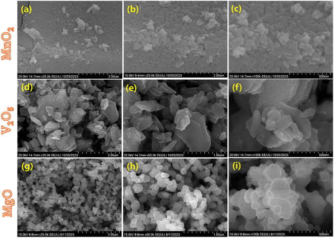
The field emission scanning electron microscopy (FESEM) images in Fig. 1a–c for MnO2, Fig. 1d–f for V2O2, and Fig. 1g–i for MgO provide a detailed view of the surface morphology of the materials, while Fig. 2a–c for MnO2, Fig. 2e–g for V2O2, and Fig. 2i–k for MgO present the images of the X-ray spectroscopy (EDX) mapping area under investigation. EDX measures the X-rays released when a sample is exposed to high-energy electrons in order to learn more about the composition of solid materials. The different concentrations of the elements across the material's surface are displayed by the individual EDX mappings of these elements in Fig. S1.† The elemental composition of the material is quantitatively analyzed by the EDX spectrum of MnO2, V2O2, and MgO in Fig. 2d, h and i, respectively. It can determine which chemical elements are present in a sample and provide an estimate of how abundant each element is relative to the other. MnO2, is known for having a certain oxygen to manganese ratio and for having a high O abundance in comparison to Mn. The elemental compositions of the compounds are as follows: Mg/O, which is composed of 39.72% magnesium and 60.28% oxygen; V/O, which is composed of 41.24% vanadium and 58.74% oxygen; and Mn/O, which is composed of 28.46% oxygen and 70.54% manganese. These compositions show the proportion of each element in the corresponding compounds, reflecting the magnesium, vanadium, manganese, and oxygen stoichiometry of each compound. The agglomerated grains are observed in the SEM images. However, the average sizes of the grains are exhibited in the nm scale. The prepared metal oxide's average grain sizes lie between 60 and 140 nm, and their profile graph result is presented in Fig. S2.† Hence, the prepared metal oxide particles show a more feasible morphology for interacting with PCBM.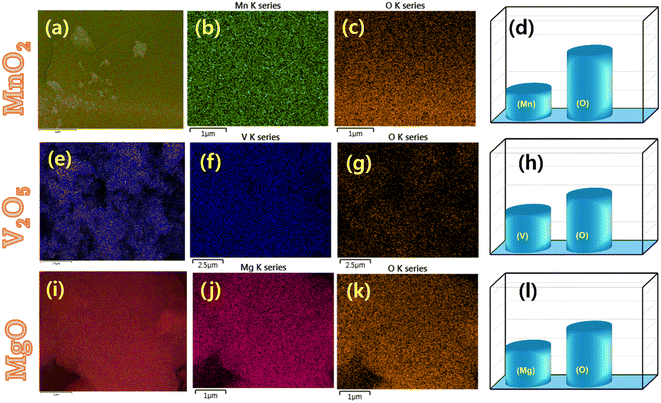 | ||
| Fig. 2 (a–c) EDX mapping of MnO2. (d) EDX spectrum of MnO2. (e–g) EDX mapping of V2O5. (h) EDX spectrum of V2O5. (i–k) EDX mapping of MgO. (l) EDX spectrum of MgO. | ||
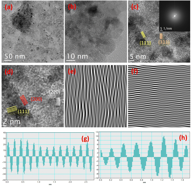
Fig. 3 shows the TEM images of MgO nanoparticles. The elevation of dispersed vertically aligned nanofringe-shaped arrays is observed in the low-resolution TEM images (Fig. 3a and b). Fig. 3c demonstrates the high-resolution images showing fringe-shaped arrays, and their inset shows the FFT pattern. The magnified image obviously elucidates the different direction-oriented arrays of grains (Fig. 3d). Fig. 3e and f shows the iFFT pattern of MgO nanoparticles. Fig. 3g and h displays the 0.21 and 0.25 nm spacing lattice profiles related to the (200) and (111) orientations, respectively.
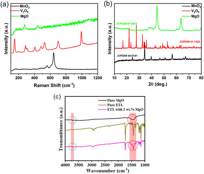
Raman measurements are utilized to assess the crystalline quality of materials. In the Raman spectra of MnO2, the peaks observed at 642 and 563 cm−1 are attributed to the stretching vibration of Mn–O bonds (Fig. 4a).26 From the V2O5 product, the prominent peak observed at 145 cm−1 wavenumber is attributed to the B3g mode of V–O–V chains, which signifies the layered structure of the V2O5 material. The peak observed at 993 cm−1 corresponds to the Ag vibration mode associated with the terminal oxygen (V![[double bond, length as m-dash]](https://www.rsc.org/images/entities/char_e001.gif) O) stretching mode. Additionally, peaks observed at 406 cm−1 and 284 cm−1 are attributed to the bending vibration of V
O) stretching mode. Additionally, peaks observed at 406 cm−1 and 284 cm−1 are attributed to the bending vibration of V![[double bond, length as m-dash]](https://www.rsc.org/images/entities/char_e001.gif) O bonds. Moreover, peaks observed at 481 cm−1 and 303 cm−1 are associated with the bending vibrations of the V–O–V and V3–O bonds, respectively. Furthermore, the V3–O stretching mode, resulting from edge-shared oxygen common to three pyramids, is identified at 524 cm−1. Lastly, the peak centered at 699 cm−1 is indicative of the V2–O stretching mode, arising from corner-shared oxygens common to two pyramids.27 The two bands observed at 276 and 442 cm−1 in the spectrum of MgO can be assigned to the transverse acoustic (TA) phonon at the zone boundary.28 The XRD spectra of MnO2 exhibit prominent peaks originating from crystallographic planes (220), (400), (330), (321), (411), (600), (710) and (202), which closely correspond to the data in JCPDS card no.: 44-0141 (Fig. 4b). Conversely, the XRD pattern of the V2O5 product reveals major peaks at orientation planes (001), (110), (101), (011), (301), (002), (020), (420), and (710), consistent with the composition of an orthorhombic structure as per the standard card JCPDS no. 41-1426. The sharp peaks observed at 2θ angles corresponding to orientation planes (200), (111), (200), (220), (311), and (440) of MgO are consistent with the data provided in the standard card JCPDS no. 87-0653, and well consistent with our TEM results (Fig. 3). On the other hand, we performed the ATR-FTIR measurement of the MgO-modified PCBM films in order to confirm the presence of MgO within the PCBM (Fig. 4c). The infrared spectral peaks at 1336–1576 cm−1 (hydroxyl group) and 3707–3752 cm−1 (–OH stretching and bending), which belong to standard MgO, are clearly seen in Fig. 4c. It confirms that MgO is present in the PCBM layer.
O bonds. Moreover, peaks observed at 481 cm−1 and 303 cm−1 are associated with the bending vibrations of the V–O–V and V3–O bonds, respectively. Furthermore, the V3–O stretching mode, resulting from edge-shared oxygen common to three pyramids, is identified at 524 cm−1. Lastly, the peak centered at 699 cm−1 is indicative of the V2–O stretching mode, arising from corner-shared oxygens common to two pyramids.27 The two bands observed at 276 and 442 cm−1 in the spectrum of MgO can be assigned to the transverse acoustic (TA) phonon at the zone boundary.28 The XRD spectra of MnO2 exhibit prominent peaks originating from crystallographic planes (220), (400), (330), (321), (411), (600), (710) and (202), which closely correspond to the data in JCPDS card no.: 44-0141 (Fig. 4b). Conversely, the XRD pattern of the V2O5 product reveals major peaks at orientation planes (001), (110), (101), (011), (301), (002), (020), (420), and (710), consistent with the composition of an orthorhombic structure as per the standard card JCPDS no. 41-1426. The sharp peaks observed at 2θ angles corresponding to orientation planes (200), (111), (200), (220), (311), and (440) of MgO are consistent with the data provided in the standard card JCPDS no. 87-0653, and well consistent with our TEM results (Fig. 3). On the other hand, we performed the ATR-FTIR measurement of the MgO-modified PCBM films in order to confirm the presence of MgO within the PCBM (Fig. 4c). The infrared spectral peaks at 1336–1576 cm−1 (hydroxyl group) and 3707–3752 cm−1 (–OH stretching and bending), which belong to standard MgO, are clearly seen in Fig. 4c. It confirms that MgO is present in the PCBM layer.
The PCBM ETL coverage is critical to the functioning of the device. We investigated how various metal oxide (MnO2, V2O5, and MgO) dopant materials affected the PCBM layer's morphology. Although the pure PCBM ETL distribution on the perovskite surface is homogeneous, it is noticeable that it contains many pinholes, as shown in Fig. 5a–c. The number of pinholes on the perovskite surface decreased significantly after introducing the metal oxide additives. Especially in case of the MgO additive (Fig. 5d), it obtained pinhole-free ETLs, which significantly contributed to effective charge transfer.
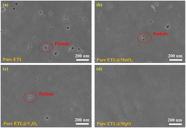 | ||
| Fig. 5 SEM images of (a) pure ETL, (b) PCBM doped with MnO2, (c) PCBM doped with V2O5, and (d) PCBM doped with MgO at the same concentration (2 wt%). | ||
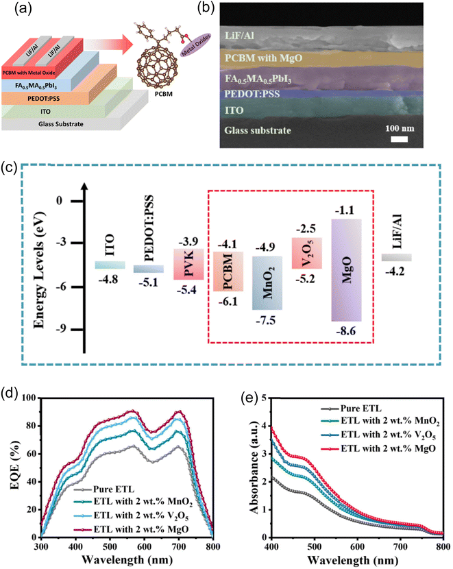
The fabricated bulk heterojunction (BHJ) PSC on a glass substrate is shown in Fig. 6a, layer by layer. An indium tin oxide (ITO) transparent electrode on a glass substrate is used in the device. A poly(3,4-ethylenedioxythiophene):poly(styrenesulfonate) (PEDOT:PSS) layer makes up the hole transport layer (HTL). FA0.5MA0.5PbI3, employed as absorber material in the device, makes up the active layer. Pure PCBM and doped PCBM incorporating metal oxides such as V2O5, MnO2, and MgO have been employed as ETLs. Following the formation of the ETL by lithium fluoride (LiF), aluminum (Al) is finally deposited as the contact material. This intricate layer arrangement offers information about the components and framework used to build the BHJ PSC for effective solar energy conversion. The FESEM image presented in Fig. 6b reveals the cross-sectional morphology of the manufactured BHJ PSC. The layered structure of the device is seen in detail in this image. The LiF/Al cathode, ITO, HTL PEDOT:PSS, active layer FA0.5MA0.5PbI3, and ETL PCBM blended with MgO are all clearly visible layers. Important information about the homogeneity of each layer and the overall structural integrity of the BHJ PSC can be gleaned from the cross-sectional viewpoint. These features are essential to comprehending and enhancing the device's performance in applications involving solar energy conversion. The energy band diagrams for each part of the PV device are shown in Fig. 6c. The active layer of the PVK is composed of FA0.5MA0.5PbI3. The LiF/Al cathode, ITO, PEDOT:PSS HTL, and ETL created by PCBM with metal oxides like V2O5, MnO2, and MgO are all traversed by the energy levels shown. This energy band alignment diagram is essential for efficient charge generation, transport, and extraction within the solar cell because it provides information about the electrical interactions taking place throughout the device's layers. MgO is incorporated into PCBM in a way that creates an advantageous configuration where the valence band is below the conduction band, making PCBM an efficient ETL for solar cells. With this arrangement, the energy gap is maximized, and the amount of energy needed for electrons to move from the valence to the conduction band is reduced. In solar cell applications, PCBM with MgO is crucial because it increases electron mobility and has a higher valence band energy than the surrounding layers. This special combination guarantees a well-aligned energy level structure within the solar cell and enhances the electron transport properties. The exact location of these energy levels is further determined by the interactions of MgO with other elements in the structure of the solar cell, highlighting its critical role in affecting the overall performance of the solar cell and assisting in increasing the efficiency in converting sunlight into electrical energy.29,30 The aforementioned discussion on the special properties of these materials can help explain the observed differences in EQE plots between devices with pure and ETL PCBM doped with V2O5, MnO2, and MgO, as depicted in Fig. 6d. When MgO is present at 2 wt%, the EQE (which estimates how well a solar cell converts incident photons to electrons) is higher than when V2O5 and MnO2 are at the same concentration. This difference can be explained by the unique properties of MgO in the structure of the solar cell.29,30 Adding MgO to PCBM results in improved electron mobility, energy gap optimization, and a higher valence band energy. A higher EQE results from these factors working together to improve the charge transport properties. However, because of variations in their energy level alignment and electron mobility, the devices containing V2O5 and MnO2 may show a relatively lower EQE. This highlights the critical role that the ETL material plays in determining the overall performance of the solar cell. The trends that have been observed emphasize the importance of material selection, with MgO being a particularly good option for maximizing the EQE in solar cell applications. The discussed properties of these materials are supported by the consistent trends seen in the UV-vis absorption spectra of pure and ETL PCBM doped with V2O5, MnO2, and MgO at the same concentration (2 wt%) throughout the wavelength spectrum from 400 nm to 800 nm (Fig. 6e). The materials' ability to absorb light at various wavelengths is revealed by the absorption spectra. The comparable absorption trends in this case suggest that MgO at 2 wt% is superior to V2O5 and MnO2 in terms of boosting light absorption within the designated wavelength range. This is explained by the special qualities of MgO, which include a higher valence band energy, enhanced electron mobility, and an optimized energy gap. These features all help to improve light absorption, which in turn raises EQE. The constancy of these patterns throughout the UV-vis spectrum highlights how crucial MgO is as an ETL for maximizing the solar cell's overall performance and optical characteristics.31
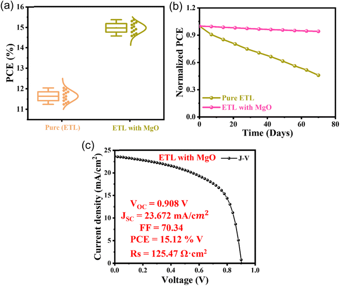
The J–V profiles are shown in Fig. 7a for various weight percentages of MnO2 (1, 1.5, 2, and 2.5 wt%) in relation to the ETL PCBM. With a peak PCE of 12.84%, the device performs exceptionally well at the ideal concentration of 2 wt% MnO2. A high open-circuit voltage (VOC) of 0.901 V, a significant short-circuit current density (JSC) of 21.795 mA cm−2, and an excellent fill factor (FF) of 65.39% serve as indicators of this. The positive J–V characteristics show how well MnO2 and PCBM were integrated into the ETL. Nevertheless, there is a noticeable drop in performance as the MnO2 concentration rises to 2.5 wt%, with decreased JSC, FF, and PCE values (21.142 mA cm−2, 64.63%, and 12.27%, respectively). The decrease in the overall device efficiency is ascribed to the formation of clusters, resulting in an elevated series resistance (RS) of 152.55 Ω cm2. This resistance hinders charge transport. A consistent trend is seen in the J–V profiles for V2O5 with different weight percentages (1, 1.5, 2, and 2.5 wt%) combined with the ETL PCBM (Fig. 7b). With a PCE of 13.97%, the device operates at peak efficiency at the ideal concentration of 2 wt% V2O5. This is characterized by a high VOC of 0.904 V, a substantial JSC of 22.638 mA cm−2, and an impressive FF of 68.26%. The J–V characteristics clearly show how well V2O5 and PCBM are integrated into the ETL, enabling efficient charge transport. On the other hand, performance is clearly diminished at higher concentrations, such as 2.5 wt% V2O5, with decreased JSC, FF, and PCE values (21.889 mA cm−2, 67.73%, and 13.24%, respectively). Cluster formation is the cause of this decrease, which results in an elevated RS of 142.62 Ω cm2, impeding charge transport and lowering total device efficiency. The J–V profiles for various MgO weight percentages combined with the ETL PCBM are shown in Fig. 7c, which shows a steady trend in the device's performance. Highest efficiency is achieved at the ideal concentration of 2 wt% MgO, where the PCE is 15.12%. A high FF of 70.34%, a significant JSC of 23.672 mA cm−2, and VOC of 0.908 V all support this. The J–V characteristics show that MgO and PCBM were well integrated in the ETL, indicating effective charge transport. On the other hand, performance slightly declines at higher concentrations, such as 2.5 wt% MgO, with decreased JSC, FF, and PCE values (22.763 mA cm−2, 68.61%, and 14.15%, respectively). This decrease can be explained by the cluster formation, which results in a marginally higher RS of 134.98 Ω cm2, which may partially impede charge transport but nevertheless retains a comparatively high efficiency when compared to lower concentrations. Finally, at higher concentrations of materials such as MnO2, V2O5, or MgO, the device structure forms clusters (as mentioned above for each case), which introduce localized regions of increased resistance and constrained pathways for charge carriers. The effective movement of electrons and holes is impeded by these clusters, which function as barriers. The higher RS linked to cluster formation hinders current flow through the device, lowering the efficiency of charge transport overall. Moreover, charge recombination, the recombination of electrons and holes prior to reaching the electrodes, can be encouraged by clusters, which would further reduce the efficiency of the device. Clusters introduce inhomogeneity that leads to non-uniform charge transport, which, in turn, reduces the efficiency of electronic devices like solar cells.32–34J–V profiles for pure and optimized (2 wt%) hybrids of MnO2, MgO, and V2O5 doped in the ETL with PCBM are shown in Fig. 7d. In comparison to the pure ETL, this has a PCE of 11.63%, and the MgO-based device exhibits the highest PCE of these hybrids, coming in at 15.12%. This indicates a significant ∼30% increase in efficiency as a result of adding MgO to the ETL with a high VOC of 0.908 V, a significant JSC of 23.672 mA cm−2, and an outstanding FF of 70.34% photovoltaic parameters. The MgO hybrid outperforms the V2O5 and MnO2 hybrids in comparison to the pure ETL with PCE values of 12.84% and 13.97%, respectively. This highlights the critical role that the MgO hybrid plays in improving electron mobility and energy band alignment.
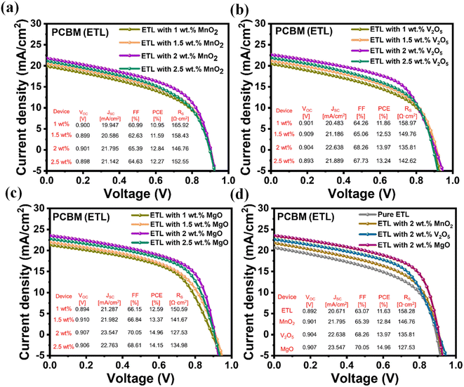 | ||
| Fig. 7 J–V profiles for 1, 1.5, 2 and 2.5 wt% of (a) MnO2, (b) V2O5, and (c) MgO doped PCBM as ETLs. (d) J–V profiles for pure and optimized (2 wt%) V2O5, MnO2, and MgO hybrids doped ETL. | ||
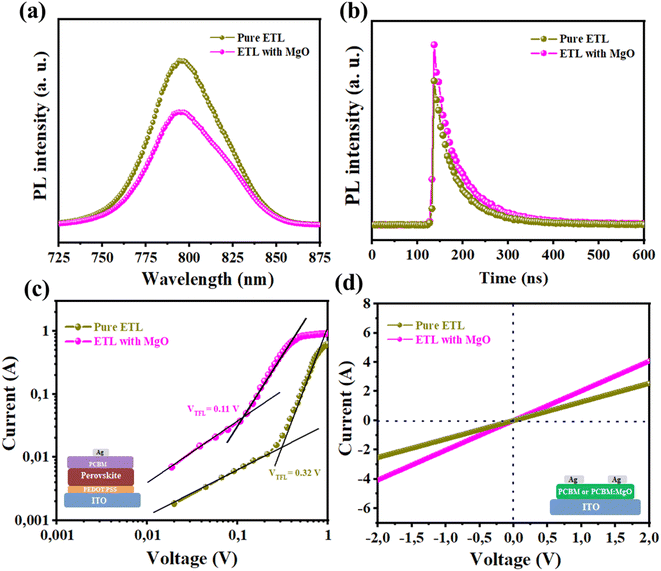
The steady-state photoluminescence (PL) and time-resolved PL spectra of the samples were measured and studied, as illustrated in Fig. 8a and b, to gain insight into the charge extraction properties of the photogenerated carriers from the hybrid perovskite to the PCBM ETL. When compared to the pure ETL film, the FA0.5MA0.5PbI3 perovskite film formed on a 2 wt% MgO-doped PCBM clearly exhibits considerable PL quenching (∼30%), demonstrating that the MgO doping has effectively increased the rate of carrier extraction at the ETL/perovskite interface.35 The perovskite film with 2 wt% MgO doped PCBM (τ2 = 148.4 ns) exhibits a shorter carrier lifetime than those of the control sample (τ2 = 385.5 ns), demonstrating that MgO-treated ETL has faster electron extraction speed from perovskite film than bare ETL, thus reducing the charge buildup and recombination loss at the perovskite/PCBM interface and improving the performance of the PSCs. In order to confirm this phenomenon and quantitatively assess the degree of trap states, we used the space-charge-limited current (SCLC) model in hole-only and electron-only device configurations in Fig. 8c. Lower trap-filled limit voltage (VTFL) was reached for the treated device (0.11 V) compared to the control device (0.32 V), as indicated in the SCLC curves of hole-only devices. These findings showed that the impact of the doping approach on the trap states is revealed by the reduction of both VTFL values in pure perovskite films following MgO doping.36,37 In order to gain a better understanding of the source of the performance boost in the MgO doping-based inverted PSC, in sandwich cells made up of ITO/ETL/Ag, with PCBM or MgO:PCBM utilized as ETLs, the I–V characteristics were examined (Fig. 8d). One can ascertain the direct current conductivity by examining the slope of the I–V plot. As seen in Fig. 8d, the MgO-doped PCBM ETL films presented higher conductivity than control films. As a result, it is expected that the photogenerated charge carriers in FA0.5MA0.5PbI3 perovskite are more efficiently transported to MgO:PCBM than to the control PCBM.23,38 The enhanced charge extraction from the perovskite-based absorber toward the ETL, which results in the observed PL quenching, is explained by the greater conductance of the MgO-based ETL.
It is clear from the PCE statistics for the 13 devices in Fig. 9a that MgO doping in PCBM significantly affects the devices' performance. According to the data, devices with pure PCBM have an average PCE of 11%, whereas devices with PCBM that have been doped with MgO have an average PCE that is significantly higher at 15%. This suggests that the addition of MgO has resulted in a noticeable increase in efficiency. Although the individual values for each of the 13 devices would shed more light on the consistency and variability of the performance enhancement, the general trend points to MgO doping as a viable approach to improving the PV performance of these devices. The average efficiency increased from 11% to 15%, indicating that the devices' performance is improved by the addition of MgO to PCBM. In the context of these devices, MgO probably improves the charge transport properties, lowers recombination losses, or helps achieve a more advantageous energy band alignment, leading to an overall improvement in efficiency. The information emphasizes how MgO works well as a dopant in PCBM to improve the devices' PV capabilities. A significant difference between the performance stability of devices with pure and MgO-doped PCBM in the ETL over a 70 day period is shown by the stability analysis shown in Fig. 9b. According to the data, devices that have PCBM doped with MgO show better stability than devices that have PCBM that is pure ETL. Over 70 days, the MgO-doped devices remain efficient, but the PCE of the pure ETL PCBM devices gradually decreases. This finding implies that adding MgO to the PCBM improves the devices' long-term stability. There are several possible reasons for the enhanced stability, including enhanced charge transport capabilities, decreased deterioration of active materials, or reduced environmental influence on the device's constituent parts. The stability analysis emphasizes that MgO doping in PCBM is a viable approach for increasing device efficiency at startup and sustaining performance over time, which is essential for the real-world use of PV devices.32,33,39,40
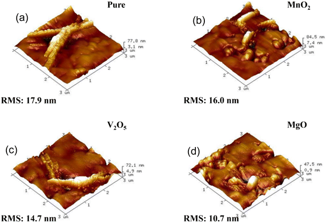
Based on the data presented in Fig. 10a–d, which shows AFM images of pure PCBM as well as PCBM doped with MnO2, V2O5, and MgO, it can be inferred that MgO-doped PCBM has better morphology than MnO2 and V2O5. The surface topography and morphology of the films are revealed by the AFM images. The claim that MgO-doped PCBM exhibits improved morphology suggests that there may be fewer irregularities or roughness on the surface, making it more uniform. The unique qualities of MgO, such as its capacity to function as a stabilizing agent, affect crystallinity, or promote better film formation during the deposition process, may be the cause of this improved morphology in MgO-doped PCBM. On the other hand, MnO2 and V2O5 might add some characteristics or clusters that have distinct effects on the surface morphology. On the PCBM surface, these materials may aggregate or form irregular structures, as indicated by the claim that MgO-doped PCBM has superior morphology in contrast. Taking everything into account, the AFM images in Fig. 10 show how different dopants impact the morphology of PCBM films, with MgO showing a more favorable surface structure than MnO2 and V2O5.41–44
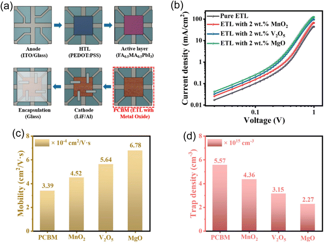
Fig. 11a describes the method of fabricating a FA0.5MA0.5PbI3 X-ray detector using metal oxide doped PCBM. The first step in the process is the deposition of the perovskite precursor onto a substrate that has been prepared. Next, metal oxide doped PCBM is added to the perovskite film. MnO2, V2O5, or MgO are examples of metal oxide dopants that are added to PCBM to improve certain characteristics. The film quality is optimized by subsequent annealing, and electrode deposition is applied to the structured device to collect the charge. The finished product is sealed to guarantee defense against external influences. In order to optimize charge transport characteristics and overall device performance, metal oxide-doped PCBM is incorporated, which adds to the X-ray detector's increased functionality. We present the logarithmic J–V (current–voltage) characteristics of MgO-doped and V2O5-doped PCBM ETL detectors (Fig. 11b). Notably, the MgO-doped ETL performs better than the other two. The dynamic range of the J–V characteristics is highlighted by the logarithmic scale. When compared to detectors doped with V2O5 and MnO2, the enhanced behavior of MgO-doped detectors indicates improved charge transport properties and superior device performance. The substantial efficiency difference is shown by the logarithmic representation, which also presents MgO as a potential dopant for improving the ETL in these detectors. The results highlight the significance of MgO in obtaining superior logarithmic J–V characteristics, indicating that it may be able to improve the devices' overall efficiency and functionality. The metal oxide dopant-MgO, for example, is emphasized because it helps achieve better morphology than V2O5 and MnO2, as the artificial X-ray detector shows. ETL doped with V2O5, MnO2, and MgO are examined for their mobility in detectors that are pure ETL PCBM (Fig. 11c). We simplified the mobility measurement by testing them under the dark or light. Using the linear fit of the log(J)–V profiles, the charge carrier mobilities were determined through the application of the Mott–Gurney relation:
The results show that the ETL doped with MgO has the highest mobility. Mobility is a key factor in figuring out how easily charge carriers pass through a material. The observation that MgO-doped detectors exhibit the highest mobility implies that the addition of MgO considerably improves charge carriers' capacity to move across the ETL. The unique characteristics of MgO, such as its effect on charge transport pathways or the crystalline structure of the ETL, may be responsible for this improvement. The findings demonstrate how beneficial MgO is as a dopant for maximizing charge carrier mobility within the ETL, which eventually leads to better performance in these detectors when compared to those doped with V2O5 and MnO2.32,39,40,45Fig. 11d displays the trap density data for detectors doped with V2O5, MnO2, and MgO, or PCBM. The data indicates that the trap density of the MgO-doped ETL is lower than those of the other dopants. A lower trap density indicates fewer defects or charge carrier trapping sites that could obstruct the free passage of charges through the material, making trap density an important parameter in semiconductor devices. The observation that MgO-doped detectors exhibit a lower trap density is consistent with MgO's superior charge transport characteristics. The extracted values from the data reveal that the MgO-doped ETL possesses the highest mobility (6.78 × 10⁻⁴ cm2 V−1 s−1) and the lowest trap density (2.27 × 1015 cm−3) among the investigated materials. This result highlights the efficiency of MgO in reducing charge carrier trapping, which enhances the overall performance of the device and makes MgO an advantageous dopant for optimizing the ETL in these detectors.39,40,46,47
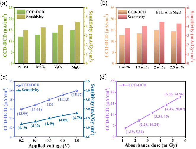
The X-ray detectors that use pure, V2O5, MnO2, and MgO-blended PCBM ETL as well as their sensitivity variations are analyzed (Fig. 12a). The results show that MgO performs better. The charge collection efficiency-dark current density (CCD–DCD) characteristics show how well the detectors gather charges and reduce dark current; MgO-doped ETL performs better than V2O5 and MnO2. The sensitivity variations highlight the beneficial effect of MgO and show that it is effective in improving the detectors' response to X-ray stimuli. When compared to V2O5 and MnO2 counterparts, MgO performs better, indicating that it plays a crucial role in improving charge collection, decreasing dark current, and boosting sensitivity. MgO-doped ETL has a CCD–DDC of 15 μA cm−2, which is higher than that of MnO2, V2O5, and pure ETL. Furthermore, MgO exhibits higher sensitivity at 4.49 mA Gy−1 cm−2 compared to MnO2 (3.86), V2O5 (4.15), and the reference ETL (3.59). As such, it is a promising dopant for attaining superior functionality in these X-ray detectors.39,40,46–48Fig. 12b shows the CCD–DCD and sensitivity characteristics for X-ray detectors with MgO-blended PCBM ETL concentrations of 1, 1.5, 2, and 2.5 wt%. The values in the figure show that performance has improved concentration-dependently. The sensitivity of CCD–DCD is 3.79 mA Gy−1 cm−2 at 1 wt%, and the measurement is 12.66 μA cm−2. The sensitivity rises to 4.05 mA Gy−1 cm−2 and the CCD–DCD improves to 13.53 μA cm−2 as the MgO concentration reaches 1.5 wt%. The CCD–DCD notably reaches 15 μA cm−2 at 2 wt%, along with a sensitivity of 4.49 mA Gy−1 cm−2, which is the highest performance among the concentrations studied. At 2.5 wt%, the sensitivity stays high at 4.31 mA Gy−1 cm−2, even though the CCD–DCD slightly drops to 14.4 μA cm−2. According to the data, the detectors perform better at 2 wt% MgO concentration, as shown by higher CCD and lower DCD values, which highlight effective charge collection and decreased dark current. Nevertheless, a decrease in performance is noted above 2 wt%, indicating that concentrations above 2 wt% may result in diminishing returns or possibly negative effects on the characteristics of the detectors. This result highlights how important the MgO concentration is for maximizing CCD–DCD and sensitivity; 2 wt% is the ideal balance for improved X-ray detector performance. The CCD–DCD and sensitivity for V2O5 and MnO2 are shown in the ESI in Fig. S4 and S5.† The CCD–DCD and sensitivity characteristics of X-ray detectors with the ETL that is blended PCBM composed of MgO are shown in Fig. 12c at different applied bias voltages. Higher applied voltages increase both CCD and sensitivity according to the data. This behavior is in line with the expected response of detectors, which are generally more sensitive and efficient at collecting charges when higher bias voltages are applied. The increase in CCD implies improved charge collection, while the rising sensitivity indicates a more responsive detection capability at higher voltages. This result highlights the significance of applied bias voltage in affecting the MgO-blended PCBM ETL X-ray detector performance and highlights the necessity of optimizing voltage conditions to obtain the intended detector characteristics. Presenting the CCD–DCD characteristics at different dose rates for X-ray detectors with the ETL made of PCBM blended with magnesium oxide, an increase is observed with higher absorbed doses (Fig. 12d). This result implies that the detectors with the MgO-blended PCBM ETL show better CCD–DCD as the dose rate or absorbed dose of X-rays increases. The responsiveness of the detectors to different exposure levels to X-rays is indicated by the correlation between CCD–DCD and the absorbed dose. This result emphasizes how MgO can be used as a dopant in PCBM ETLs to improve X-ray detector performance, especially in situations where dose rates are higher.
4. Conclusion
In conclusion, our study on the ETL PCBM for PSCs X-ray and detectors with metal oxide dopants (V2O5, MnO2, and MgO) emphasises the crucial role MgO plays in enhancing device efficiency. The PSC outperforms its V2O5 and MnO2 counterparts, achieving a peak PCE of 15.12% when optimized with 2 wt% MgO in the ETL. Additionally, X-ray detectors benefit greatly from this ideal MgO concentration, showing increased sensitivity, decreased dark current, and enhanced charge collection efficiency. The influence of MgO on the surface morphology and elemental composition is demonstrated by comprehensive characterization methods such as EDX and FESEM. The concentration-dependent analyses highlight 2 wt% MgO as the optimal ratio for better results in X-ray detectors and PSCs. These results highlight the versatility and potential of MgO for future advancements in electronic devices while contributing to our understanding of metal oxide dopants in electronic devices and offering hope for applications in medical imaging and renewable energy.Data availability
The data that support the findings of this study are available from the corresponding author upon reasonable request. The data are not publicly available due to privacy and ethical restrictions.Conflicts of interest
The authors declare that there are no competing financial interests.Acknowledgements
This work was supported by the National Research Foundation of Korea (NRF) grant funded by the Korean government (MSIT) (No. RS-2022-00165798). The authors also thank the Researchers Supporting Project number (RSP2024R266), King Saud University, Riyadh, Saudi Arabia, for their financial support.References
- S. Aftab, M. Z. Iqbal, S. Hussain, F. Kabir, A. A. Al-Kahtani and H. H. Hegazy, Adv. Funct. Mater., 2023, 2303449 CrossRef CAS.
- S. Aftab, A. Abbas, M. Z. Iqbal, S. Hussain, F. Kabir, H. H. Hegazy, F. Xu, J. H. Kim and B. S. Goud, Mater. Today Energy, 2023, 101366 CrossRef CAS.
- S. Aftab, M. Z. Iqbal, S. Hussain, H. H. Hegazy and M. A. Saeed, Nano Energy, 2023, 108, 108249 CrossRef CAS.
- S. Aftab, M. Z. Iqbal, H. H Hegazy, S. Azam and F. Kabir, Nanoscale, 2023, 15(8), 3610–3629 RSC.
- B. Parida, A. Singh, A. K. Kalathil Soopy, S. Sangaraju, M. Sundaray, S. Mishra, S. Liu and A. Najar, Advanced Science, 2022, 9, 2200308 CrossRef PubMed.
- A. K. Nasr, M. K. Kashan, A. Maleki, N. Jafari and H. Hashemi, Entrepreneurship and Sustainability Issues, 2020, 7, 2526 CrossRef.
- J. Tang, H. Liu, D. Zhitomirsky, S. Hoogland, X. Wang, M. Furukawa, L. Levina and E. H. Sargent, Nano Lett., 2012, 12, 4889–4894 CrossRef CAS.
- S. Aftab, M. Z. Iqbal, S. Hussain, H. H. Hegazy and M. A. Saeed, Nano Energy, 2023, 108249 CrossRef CAS.
- S. Aftab, A. Abbas, M. Z. Iqbal, S. Hussain, F. Kabir, H. H. Hegazy, F. Xu, J. H. Kim and B. S. Goud, Mater. Today Energy, 2023, 36, 101366 CrossRef CAS.
- S. Aftab, M. Z. Iqbal, S. Hussain, F. Kabir, S. Kumar, H. Hegazy and B. S. Goud, J. Mater. Chem. C, 2023, 11, 13189–13203 RSC.
- E. Akman, T. Ozturk, W. Xiang, F. Sadegh, D. Prochowicz, M. M. Tavakoli, P. Yadav, M. Yilmaz and S. Akin, Energy Environ. Sci., 2023, 16, 372–403 RSC.
- R. Azmi, S. Zhumagali, H. Bristow, S. Zhang, A. Yazmaciyan, A. R. Pininti, D. S. Utomo, A. S. Subbiah and S. De Wolf, Adv. Mater., 2023, 2211317 Search PubMed.
- T. Ozturk, E. Akman, B. Surucu, H. Dursun, V. Ozkaya and S. Akin, Eur. J. Inorg. Chem., 2021, 2021, 4251–4264 CrossRef CAS.
- Y. Wang, A. B. Djurišić, W. Chen, F. Liu, R. Cheng, S. P. Feng, A. M. C. Ng and Z. He, J. Phys.: Energy, 2020, 3, 012004 Search PubMed.
- L. Zhang, C. Fu, S. Wang, M. Wang, R. Wang, S. Xiang, Z. Wang, J. Liu, H. Ma and Y. Wang, Adv. Funct. Mater., 2023, 33, 2213961 CrossRef CAS.
- H. Wu, Y. Ge, G. Niu and J. Tang, Matter, 2021, 4, 144–163 CrossRef CAS.
- D. Angmo, X. Peng, J. Cheng, M. Gao, N. Rolston, K. Sears, C. Zuo, J. Subbiah, S.-S. Kim and H. Weerasinghe, ACS Appl. Mater. Interfaces, 2018, 10, 22143–22155 CrossRef CAS.
- J. Han, H.-Y. Wang, Y. Wang, M. Yu, S. Yuan, P. Sun, Y. Qin, Z.-X. Guo, J.-P. Zhang and X.-C. Ai, RSC Adv., 2016, 6, 112512–112519 RSC.
- C. Tian, G. Betancourt-Solis, Z. Nan, K. Liu, K. Lin, J. Lu, L. Xie, L. Echegoyen and Z. Wei, Sci. Bull., 2021, 66, 339–346 CrossRef CAS.
- M. Jiang, Q. Niu, X. Tang, H. Zhang, H. Xu, W. Huang, J. Yao, B. Yan and R. Xia, Polymers, 2019, 11, 147 CrossRef PubMed.
- J. Liu, G. Wang, K. Luo, X. He, Q. Ye, C. Liao and J. Mei, ChemPhysChem, 2017, 18, 617–625 CrossRef CAS.
- A. Agresti, S. Pescetelli, L. Cinà, D. Konios, G. Kakavelakis, E. Kymakis and A. D. Carlo, Adv. Funct. Mater., 2016, 26, 2686–2694 CrossRef CAS.
- Z. Yang, J. Xie, V. Arivazhagan, K. Xiao, Y. Qiang, K. Huang, M. Hu, C. Cui, X. Yu and D. Yang, Nano Energy, 2017, 40, 345–351 CrossRef CAS.
- A. A. Qureshi, E. R. Schütz, S. Javed, L. Schmidt-Mende and A. Fakharuddin, Energy Adv., 2023, 2, 1905–1914 RSC.
- J. Zhang, C. H. Tan, T. Du, M. Morbidoni, C.-T. Lin, S. Xu, J. R. Durrant and M. A. McLachlan, Sci. Bull., 2018, 63, 343–348 CrossRef CAS.
- V. Sannasi and K. Subbian, J. Mater. Sci.: Mater. Electron., 2020, 31, 17120–17132 CrossRef CAS.
- N. M. Abd-Alghafour, G. A. Naeem and S. M. Mohammad, J. Phys.: Conf. Ser., 2020, 1535(1), 012046 CrossRef CAS.
- N. S. Awwad, A. M. Alshahrani, K. A. Saleh and M. S. Hamdy, Molecules, 2017, 22, 1947 CrossRef PubMed.
- S. Mohapatra, T. A. Nguyen and P. Nguyen-Tri, Noble Metal-Metal Oxide Hybrid Nanoparticles: Fundamentals and Applications, Elsevier, 2018 Search PubMed.
- E. Cavaliere, G. Benetti, F. Banfi and L. Gavioli, Front. Nanosci., 2020, 2020, 291–311 Search PubMed.
- S. N. Vodapally and M. H. Ali, Energies, 2022, 16, 319 CrossRef.
- P.-H. Lee, T.-T. Wu, K.-Y. Tian, C.-F. Li, C.-H. Hou, J.-J. Shyue, C.-F. Lu, Y.-C. Huang and W.-F. Su, ACS Appl. Mater. Interfaces, 2020, 12, 45936–45949 CrossRef CAS.
- F. Jafari, B. R. Patil, F. Mohtaram, A. L. F. Cauduro, H.-G. Rubahn, A. Behjat and M. Madsen, Sci. Rep., 2019, 9, 10422 CrossRef PubMed.
- Z. Wang, D. Yang and T.-K. Sham, Surf. Sci., 2018, 676, 71–76 CrossRef CAS.
- E. Akman and S. Akin, Adv. Mater., 2021, 33, 2006087 CrossRef CAS.
- D. Yang, X. Zhang, K. Wang, C. Wu, R. Yang, Y. Hou, Y. Jiang, S. Liu and S. Priya, Nano Lett., 2019, 19, 3313–3320 CrossRef CAS.
- M. K. A. Mohammed, M. I. Abualsayed, A. M. Alshehri, A. Kumar, M. Dehghanipour, R. Sh Alnayli, S. Aftab and E. Akman, ACS Appl. Energy Mater., 2024, 7(3), 1358–1368 CrossRef CAS.
- G. Kakavelakis, T. Maksudov, D. Konios, I. Paradisanos, G. Kioseoglou, E. Stratakis and E. Kymakis, Adv. Energy Mater., 2017, 7, 1602120 CrossRef.
- S. Hussain, H. Liu, D. Vikraman, S. H. A. Jaffery, G. Nazir, F. Shahzad, K. M. Batoo, J. Jung, J. Kang and H.-S. Kim, Nanoscale, 2023, 15, 7329–7343 RSC.
- Z. Zhu, Q. Xue, H. He, K. Jiang, Z. Hu, Y. Bai, T. Zhang, S. Xiao, K. Gundogdu and B. R. Gautam, Advanced Science, 2016, 3, 1500353 CrossRef PubMed.
- L. Liirò-Peluso, J. Wrigley, D. B. Amabilino and P. H. Beton, ACS Appl. Nano Mater., 2022, 5, 13794–13804 CrossRef PubMed.
- E. M. Mkawi, Y. Al-Hadeethi, B. Arkook and E. Bekyarova, Materials, 2023, 16, 2218 CrossRef CAS.
- S. Shah, Nano Express, 2020, 1, 020037 CrossRef.
- L. Liirò-Peluso, J. Wrigley, D. B. Amabilino and P. H. Beton, ACS Appl. Nano Mater., 2022, 5, 13794–13804 CrossRef.
- S. Luan, Y. Liu, Y. Wang and R. Jia, Mater. Lett., 2018, 217, 139–142 CrossRef CAS.
- S. Luan, Y. Liu, Y. Wang and R. Jia, Mater. Lett., 2018, 217, 139–142 CrossRef CAS.
- Z. Bin, J. Li, L. Wang and L. Duan, Energy Environ. Sci., 2016, 9, 3424–3428 RSC.
- S. Demchyshyn, M. Verdi, L. Basiricò, A. Ciavatti, B. Hailegnaw, D. Cavalcoli, M. C. Scharber, N. S. Sariciftci, M. Kaltenbrunner and B. Fraboni, Advanced Science, 2020, 7, 2002586 CrossRef CAS.
Footnotes |
| † Electronic supplementary information (ESI) available. See DOI: https://doi.org/10.1039/d4ta03785e |
| ‡ These authors are contributed equally. |
| This journal is © The Royal Society of Chemistry 2024 |

