Advances in direct optical lithography of nanomaterials
Yuelin
Yang†
,
Jie
Guan†
,
Nannan
Zhang
,
Lin
Ru
,
Yihao
Zou
and
Yuanyuan
Wang
 *
*
State Key Laboratory of Coordination Chemistry, School of Chemistry and Chemical Engineering, Nanjing University, Nanjing 210093, China. E-mail: wangyy@nju.edu.cn
First published on 5th November 2024
Abstract
The precise assembly of nanomaterials is essential for integrating nanomaterials into sophisticated devices. However, conventional nanoscale patterning methods face obstacles such as high cost, low resolution, and environmental contamination. Direct optical lithography is used to fabricate photosensitive nanomaterials using surface engineering and utilizes the photochemical reactions of ligands to alter their solubility, enabling optical patterning. This method, which does not rely on polymer photoresists, holds great potential as an emerging lithographic technology. This approach simplifies the lithography process, reduces costs, and minimizes the environmental impact. In this review, we begin with an in-depth analysis of the evolution of optical lithography and key optical pattern strategies. We then emphasize how advanced nanomaterials, such as quantum dots, metal oxides, metals, clusters, and metal–organic frameworks, contribute to precise patterning for electronic and optoelectronic applications. Finally, we discuss current challenges in this field and propose solutions to improve patterning efficiency and quality while addressing issues about environmental sustainability.
1 Introduction
Nanomaterials are characterized by having at least one dimension of 100 nm or smaller. Due to their unique size and surface effects, such as high specific surface area, quantum size effects, and surface effects, nanomaterials exhibit superior physicochemical properties.1,2 These properties endow nanomaterials with broad application potential in various fields, including energy, biomedicine, information technology, and environmental science.3–11 In order to fully utilize the potential of nanomaterials in the construction of high-tech devices, it is essential to achieve efficient and precise directed assembly. This process is crucial for the creation of microelectronic devices, optoelectronic devices, and sensors, where the distinctive properties of nanomaterials can be optimally employed.12Over the past few decades, a variety of patterning techniques for nanomaterials have been developed, including stimulus-based methods such as optical lithography,13–15 electron-beam lithography,16–18 and thermal lithography,19–21 as well as physical methods such as inkjet printing22–24 and transfer printing.25–27 Each technique has its own advantages and limitations. For example, electron-beam lithography can achieve sub-10 nm resolutions, but applying resist films to non-planar substrates is challenging due to the limitations of spin coating.28,29 Thermal lithography, particularly thermal scanning probe lithography (t-SPL), also offers high-resolution patterning down to sub-10 nm resolution. However, its application is limited by throughput and potential tip degradation.30,31 Inkjet printing is cost-effective and suitable for large-area patterning, but the resolution of inkjet printing in nanoscale applications is relatively low, typically in tens to hundreds of microns.32,33
Optical lithography is an essential technique for nanomaterial patterning, playing a significant role in the development of microelectronic devices, optoelectronic devices, and sensors due to its high resolution and repeatability.34 The traditional optical lithography process involves exposing and developing geometric structures on a photoresist layer, followed by an etching process to transfer the pattern onto the substrate. There are two primary methods to pattern nanomaterials by using traditional optical lithography: using polymer photoresists as templates or mixing polymer photoresists with the materials for lithography. However, both approaches have their own challenges. When using a photoresist as a template, uneven thickness or defects in the photoresist will directly affect the quality of the pattern and the performance of the device.35 Moreover, the photoresist may expand or contract during exposure and development, which can also cause pattern distortion. Although the method of mixing the photoresist can reduce some issues of thickness and uniformity, impurities or bubbles may be introduced during the mixing process, affecting the optoelectronic performance of the material.36 At the same time, the compatibility of photoresists with nanomaterials is also an issue that needs to be considered.37 To overcome these problems, researchers explored polymer photoresist-free patterning methods. Photoresist-free lithography, also known as direct optical lithography, achieves patterning through direct photochemical action, avoiding polymer photoresists. This method has the advantage of achieving higher pattern accuracy and better device performance while simplifying the manufacturing process and reducing costs, as well as reducing the impact on the environment.37–47
The research on direct optical lithography focuses on the development of new types of photosensitive inks tailored to various applications. These unique inks consist of nanomaterials that require patterning and can be prepared in three ways: without photosensitive molecules,48 utilizing photosensitive molecules as ligands,38,43,49–51 or incorporating photosensitive molecules as additives.47,51–57 This approach not only expands the application scope of nanomaterials but also enhances their potential uses. In addition, direct optical lithography is gradually overcoming the challenges of conventional lithography techniques by directly patterning materials through photochemical processes, offering new solutions for micro- and nano-manufacturing.
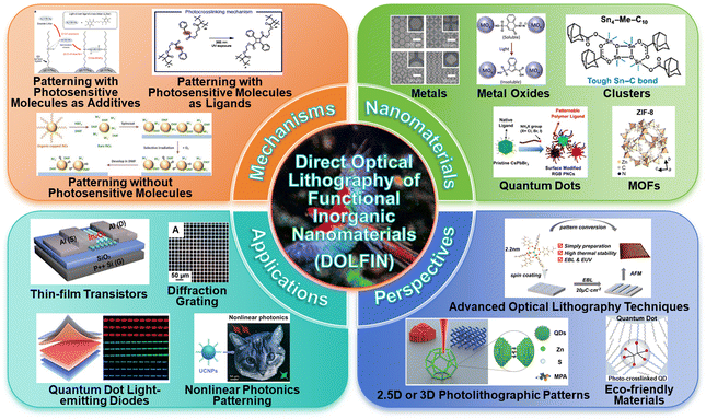
In this review, we provided an in-depth look at the evolution of optical lithography, focusing on the benefits and challenges of direct optical lithography. We highlighted the Direct Optical Lithography of Functional Inorganic Nanomaterials (DOLFIN) process and discussed three key pattern design strategies. We emphasized the role of advanced nanomaterials, such as quantum dots (QDs), metal oxides, metals, clusters, and metal–organic frameworks (MOFs), in achieving precise patterning for applications in electronics and optoelectronics. Finally, we addressed the current challenges in direct optical lithography and proposed solutions to improve patterning efficiency and quality, while considering environmental sustainability and the development of multi-level patterning technologies to advance the field (Scheme 1).
2 The background and development of optical lithography of nanomaterials
2.1 The evolution of direct optical lithography
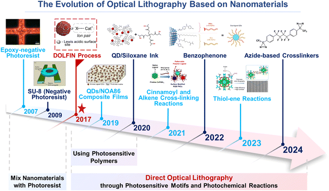
The evolution of materials science has marked a significant transition in lithography technology from traditional to direct optical lithography (Fig. 1). Traditional lithography, dependent on photoresists as a photosensitive medium and involving pattern transfer through exposure and development, presents challenges in material adaptability and potential interference with the optoelectronic properties of materials.58,59 Direct optical lithography has emerged as a solution, enabling patterning by modifying the chemical properties of the material surface, eschewing the need for photoresists.37–47 This method is particularly adept at patterning nanomaterials such as QDs, facilitating high-precision patterning without compromising material integrity.The progression of direct optical lithography has been remarkable. Advances in functional inorganic materials and photoresists have been integral to the development of optical lithography. Photoresists are key materials for transferring microfabricated patterns and are often used as polymer formulations to assist in patterning nanomaterials in traditional optical lithography. Functional inorganic materials can be used as one of the components of photoresists and, at the same time, can be directly patterned in direct optical lithography applications. Photoresists, one of the focuses of research in traditional optical lithography, are critical for enabling micro- and nanofabrication and the precise patterning of integrated circuits.60–66 Initially, researchers used well-established traditional optical lithography to combine nanomaterials with photoresists to simplify the patterning process. This phase facilitated the introduction of photoresists with different material compositions, including epoxy-negative photoresists60 and commercial photoresists (SU-8 (ref. 61 and 62) and EOC series66), and these photoresist products are still widely used today. However, the inherent incompatibility between nanomaterials and typical photoresists posed challenges in achieving homogeneous dispersion.67–71 To counter this, researchers explored alternative photosensitive polymers and surface modifications to enhance the compatibility and uniform dispersion of nanomaterials within polymer matrices. Subsequently, the concept of polymer photoresist-free, direct optical lithography of functional inorganic nanomaterials was introduced, offering an alternative patterning approach that capitalizes on the design of photoactive ligands. This method, proposed by Talapin's group in 2017, retains the advantages of traditional optical lithography while being inherently adaptable to material-specific requirements and eliminating the need for a polymeric photoresist.38
As research progressed, the focus shifted from merely achieving patterning quality to exploring the various applications of patterned nanomaterials. Numerous direct photolithographic techniques have been demonstrated to have non-destructive or even beneficial effects on the properties of nanomaterials. These methods not only enhanced the properties of nanomaterials but also ensured the quality of patterns. The exploration of stimulus-sensitive ligands that respond to light irradiation has opened new avenues for nanomaterial patterning. Photosensitive ligands and photochemical reactions, such as azide,37,41,46,72 benzophenone,45 cinnamoyl,43 photo-acid generation,52 oxime sulfonate,73 thiol-ene,56,58,74 photo-amine generation,53 oxide bridging,75 photo-oxidation,48 and alkene cross-linking,43,76,77 have been successfully employed for direct photopatterning of nanomaterials.
Today, researchers are increasingly focusing on the practical applications of patterned nanomaterials, extending the use of direct optical lithography to various materials and fields. The pursuit of higher resolution, 3D patterning, and multimaterial integration continues to drive innovation in this area, all while preserving the optoelectronic properties of the materials.38,78,79 The future of direct optical lithography holds the promise of integrating nanomaterials into sophisticated photonic and electronic devices, marking a significant step towards the commercialization of advanced technologies.
2.2 Direct optical lithography of functional inorganic nanomaterials (DOLFIN)
In 2017, the Talapin group introduced a groundbreaking technique known as Direct Optical Lithography of Functional Inorganic Nanomaterials (DOLFIN). This method revolutionizes the field of nanomaterial patterning by bypassing the need for traditional photoresists.38 This innovative approach utilized photosensitive inorganic ligands, such as photoacid generators (PAGs) and ammonium 1,2,3,4-thiatriazole-5-thiolate (TTT, NH4CS2N3), which underwent chemical transformations upon ultraviolet (UV) irradiation. This reaction modified the solubility of nanocrystals (NCs) in a developer solution, enabling direct patterning of various functional inorganic materials (Fig. 2A).49 The chemical reactivity of these surface ligands, as depicted in Fig. 2B, allowed for precise control over the patterning process without compromising the material's electronic and optical properties, which is essential for high-performance device fabrication.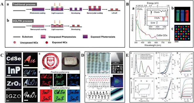 | ||
| Fig. 2 Schematic overview of lithographic techniques. (A) Traditional optical lithography process (a) and DOLFIN process (b).49 Copyright 2019, American Chemical Society. (B) Examples of various inorganic materials patterned using DOLFIN technology with PAG+-based and CS2N3− ligands. (C) Optical patterning of different materials with photosensitive inorganic ligands. (D) Typical pattern characteristics achieved with DOLFIN technology, including multilayer patterning of CdSe NCs using NH4CS2N3 ligands and control over thickness and resolution through the use of various ligands. (E) The properties of directly optically patterned semiconductor and dielectric materials, illustrating the preservation of material integrity and performance post-patterning, as evidenced by sharp photoluminescence spectra, dielectric constants, and the electrical characteristics of prototype FETs.38 Copyright 2017, American Association for the Advancement of Science. | ||
DOLFIN's versatility was evident in its ability to operate across a wide range of photon energies, including deep ultraviolet (DUV, 254 nm), near-ultraviolet (365 nm), blue (405 nm), and visible light (450 nm).49 This broad applicability facilitated high-resolution patterning of diverse inorganic materials such as semiconductors, metals, oxides, and magnetic materials, as shown in Fig. 2C and D.38 The process was designed to maintain the absorption spectra and morphological features of the materials, which was crucial for applications in electronic circuits, sensor arrays, and high-definition displays. In addition, DOLFIN's compatibility with various substrates, including silicon, glass, and polymers, opened up possibilities for the development of hybrid devices. The potential application area of this technology included the fabrication of electronic and optoelectronic devices such as light-emitting diodes (LEDs), field-effect transistors (FETs), photodetectors, and solar cells (Fig. 2E). It also enabled the precise patterning required for sensor arrays and high-definition quantum dot light-emitting diodes (QLEDs), showcasing its broad utility in nanofabrication.38 The introduction of DOLFIN marks a significant milestone in nanofabrication technology. This technology provides a more efficient and versatile complement to traditional photopolymer lithography for patterning nanomaterials and device fabrication. By enhancing performance and reliability, it holds the potential to shape the future of electronic and optoelectronic device manufacturing.
2.3 Key parameters for direct optical lithography
Direct optical lithography has emerged as a powerful technique for fabricating high-resolution patterns of functional inorganic nanomaterials. In pursuit of the optimization of direct optical lithography technology, this article integrates the current outstanding research findings in direct optical lithography and summarizes several critical parameters of the technology, including:37,42,79,80(1) Light source and wavelength. Depending on the properties of the nanomaterials and the desired pattern characteristics, choosing an appropriate wavelength can optimize the quality and resolution of the pattern. For example, shorter wavelengths (e.g., DUV) can provide higher resolution. However, they may damage some materials, while longer wavelengths (e.g., near-ultraviolet or visible light) can penetrate thicker films but may have lower resolution.
(2) Exposure dose. The exposure dose needs to be precisely controlled according to the photosensitivity of the nanomaterials and the resolution requirements of the patterns. The exposure dose, measured in mJ cm−2, is a critical factor directly influencing the degree of solubility change in the nanomaterial film. An optimal exposure dose ensures that the film undergoes the intended photochemical transformations, such as cross-linking or desorption of ligands, without degrading the material's properties or inducing unwanted side reactions.
(3) Developer solvent. The ideal developer solvent can be used to differentiate between exposed and unexposed regions of the nanomaterial film. Parameters such as the developer's polarity, solvency, and compatibility with the nanomaterials are critical in the selection process.
Direct optical lithography is essential for achieving high-resolution and high-performance patterning of inorganic nanomaterials. The following sections will provide an in-depth discussion of the optimization of these patterning parameters, with a focus on various nanomaterial patterning examples. This discussion aims to offer the reader a thorough understanding of how the patterning process can be tailored for different applications.
2.4 Optimization strategies for nanomaterial patterning
Great breakthroughs have been made in direct optical lithography of nanomaterials. Nevertheless, there are still some aspects that need to be considered.Exploring stimulus-sensitive molecules in patterning. Most current researchers have investigated diverse photosensitive molecules that can be used for direct nanomaterials patterning so that the direct optical lithography process for nanomaterials has much space for development. Future development of stimulus-sensitive molecules would build upon these established reported molecule families and involve more careful chemical design with specific targets in terms of stimulus, nanomaterials type, and pattern properties, followed by custom molecules synthesis.48,81–86
Developing a wide range of patternable materials. Most of the current direct optical lithography patterning strategies have been proven to be suitable for stable group II–VI semiconductor QD materials. However, realizing nondestructive patterning of unstable QDs (such as perovskite and III–V QDs) is more challenging, so the compatibility of the nanomaterial surface and direct optical lithography technique should be studied from the perspective of photochemical nature. Therefore, these strategies would be preferably extended to other functional nanomaterials in the future.47,52–56
Focusing on the quality of direct optical lithography patterning. The optimization and innovation of the optical lithography process will be the main direction of the future development of direct optical lithography patterning for nanomaterials, which would provide greater impetus for the advancement of high-resolution patterning technology. Ideally, the patterning for nanomaterials should simultaneously satisfy the following set of requirements: (i) high resolution, ideally sub-micrometers, (ii) high throughput, (iii) high fidelity, (iv) a uniform pattern profile, and (v) no contamination or damage of their own performance during the patterning process.47,49,78
In the following sections, we provide a detailed account of the advantages and challenges of direct optical lithography. First, we summarize the three main methods of direct optical lithography: patterning using photosensitive molecules as ligands, patterning with photosensitive molecules as additives, and patterning without photosensitive molecules. Then we provide a comprehensive overview of the nanomaterials currently amenable to direct patterning, including QDs, metal oxides, metals, clusters, and MOFs. Finally, in light of the ongoing discourse on the quality issues associated with direct optical lithography patterning, we will explore various application scenarios for this technique.
3 Mechanisms of direct optical lithography for nanomaterial patterning
A profound comprehension of its underlying mechanisms is required to harness the opportunities and challenges of direct optical lithography. This foundational knowledge is crucial for enhancing the performance of photosensitive nanomaterials and for propelling the technology forward to satisfy the stringent requirements of high-resolution patterning across diverse applications. The essence of direct optical lithography lies in the creation of photosensitive nanomaterials through surface engineering, which enables the alteration of the solubility of these nanomaterials in their respective solvents upon exposure to specific wavelengths of light, thereby facilitating the formation of patterns.38 In this advancement, photosensitive nanomaterials are predominantly fabricated by incorporating photosensitive molecules. The approaches to achieve this are categorized based on the role of these photosensitive molecules.In this section, we summarized three distinct mechanisms of direct optical lithography: patterning using photosensitive molecules as ligands, patterning with photosensitive molecules as additives and patterning without photosensitive molecules. These mechanisms directly alter the solubility of nanomaterials, further enabling optical patterning. Exploration of these mechanisms is important, because it paves the way for innovative applications and advances in the fields of nanotechnology and materials science.
3.1 Patterning with photosensitive molecules as ligands
The synthesis of nanomaterials typically requires encapsulation with alkyl ligands, which is crucial for maintaining a stable dispersion and passivating surface dangling bonds, thereby preventing aggregation or unwanted chemical reactions. However, the inherent chemical stability of these alkyl ligands poses challenges for direct optical lithography, as this technique relies on the transformation of ligands under light exposure to form patterns. Traditionally, such transformations depend on high-energy irradiation sources, such as electron beams (e-beams) or X-rays, which can induce chemical changes in the ligands, allowing for the creation of nanoscale patterns.87–91 Unfortunately, the need for such high-energy sources limits the accessibility and scalability of this technology.To address this issue, researchers have been exploring the use of photosensitive molecules as ligands—these ligands can initiate chemical reactions under lower energy light, such as the light available in standard optical lithography setups. These photosensitive ligands undergo photochemical reactions upon exposure to light, leading to cross-linking or other structural changes that effectively “lock” the nanomaterials into the desired area. The unexposed areas can then be easily washed away, enabling more convenient and efficient direct optical lithography.38,49
Direct optical lithography mechanisms using photosensitive ligands involve a photoinitiated process, where light triggers a series of chemical events within the ligand molecules. The absorbed photons excite the ligands to a higher energy state, promoting the formation of reactive intermediates that engage in cross-linking reactions with neighboring ligands or the substrate.47,49 This cross-linking reaction secures the nanomaterials in the exposed areas, forming stable patterns that withstand the development process, which removes the uncross-linked, mobile nanomaterials. By adjusting the photosensitivity range of the ligands, it is possible to achieve nanoscale patterning using light sources of different energies, such as 254 nm, 365 nm, and 405 nm.43,50,51
DOLFIN, a groundbreaking strategy initially proposed by Talapin and coworkers, leveraged the characteristics of compact photosensitive surface ligands that undergo changes under controlled light exposure.38 These ligands provided colloidal stability to nanomaterials and undergo chemical reactions upon photon absorption, altering the solubility of nanomaterials in the development solution. In their pioneering study, the authors designed photochemically active anionic (X−) and cationic (Cat+) groups, such as NH4CS2N3 and diphenyliodonium (Ph2I+) or triphenylsulfonium (Ph3S+) cations, respectively. As shown in Fig. 3A, these groups could function as photosensitive ligands either by covalently attaching to the nanomaterial surface or through ion-pair interactions. Initially, the sensitivity of these ligands was limited to 254 nm photons, corresponding to DUV. Subsequent advancements led to the development of ligand systems responsive to a broader range of photon energies, thereby expanding the applicability of the technique. As detailed in Fig. 3B, this innovation allowed the direct patterning of nanomaterials not only with UV light but also with near-UV light (365 nm), blue light (405 nm), and visible light (450 nm).49
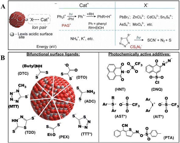 | ||
| Fig. 3 The strategy of employing photosensitive molecules as photoreactive ligands for direct optical lithography. (A) Schematic representation of a nanocrystal with ion pair surface ligands and two complementary approaches to the design of photosensitive inorganic ligands.38 Copyright 2017, American Association for the Advancement of Science. (B) Chemical structures of designed photoactive ligands used for DOLFIN.49 Copyright 2019, American Chemical Society. | ||
Building upon this work, the field has advanced by combining short, photo-decomposable ion-pair ligands with polymer molecules containing cross-linkable fragments, developing photosensitive ligands capable of directly patterning nanomaterials. These ligands can undergo cyclization and polymerization reactions under UV irradiation. A typical example was the cross-linking reaction of ligands containing alkene groups, where the UV-induced cleavage of C![[double bond, length as m-dash]](https://www.rsc.org/images/entities/char_e001.gif) C bonds led to the formation of new C–C bonds (Fig. 4A).43 This cross-linking mechanism has been extensively utilized in the synthesis of photosensitive ligands for nanomaterial patterning. For example, Bang and colleagues synthesized a multifunctional polymer ligand, ammonium halide-terminated poly(2-cinnamoyloxyethyl methacrylate) (PCEMA–NH3X, where X = Cl, Br, I), to facilitate the patterning of nanomaterials through direct optical lithography (Fig. 4B).43 Additionally, Kim et al. demonstrated the application of azide-containing molecular ligands, such as 4-(2-azidoethyl)benzoic acid (AzL1) and 4-(4-azidobutoxy)benzoic acid (AzL2), in patterning.50 Azides are known to generate nitrene radicals under DUV light irradiation, which can insert into C–H bonds, enabling chemical cross-linking between neighboring nanomaterials when azide-containing ligands are present on their surface. Following a similar strategy, Ko et al. designed a random copolymeric ligand, poly(vinyltriphenylamine-random-azidostyrene) (P(TPA-r-SN3)-SH), for the purpose of nanomaterial patterning (Fig. 4C).51 Benzophenone is another photoactive group that can undergo crosslinking reactions with neighboring aliphatic chains under UV light. Recently, Bae et al. demonstrated direct optical patterning nanomaterials by incorporating photo-crosslinkable ligands containing benzophenone derivatives (Fig. 4D).45 These advancements highlight the versatility and efficacy of photosensitive ligands in the precise and efficient patterning of nanomaterials.
C bonds led to the formation of new C–C bonds (Fig. 4A).43 This cross-linking mechanism has been extensively utilized in the synthesis of photosensitive ligands for nanomaterial patterning. For example, Bang and colleagues synthesized a multifunctional polymer ligand, ammonium halide-terminated poly(2-cinnamoyloxyethyl methacrylate) (PCEMA–NH3X, where X = Cl, Br, I), to facilitate the patterning of nanomaterials through direct optical lithography (Fig. 4B).43 Additionally, Kim et al. demonstrated the application of azide-containing molecular ligands, such as 4-(2-azidoethyl)benzoic acid (AzL1) and 4-(4-azidobutoxy)benzoic acid (AzL2), in patterning.50 Azides are known to generate nitrene radicals under DUV light irradiation, which can insert into C–H bonds, enabling chemical cross-linking between neighboring nanomaterials when azide-containing ligands are present on their surface. Following a similar strategy, Ko et al. designed a random copolymeric ligand, poly(vinyltriphenylamine-random-azidostyrene) (P(TPA-r-SN3)-SH), for the purpose of nanomaterial patterning (Fig. 4C).51 Benzophenone is another photoactive group that can undergo crosslinking reactions with neighboring aliphatic chains under UV light. Recently, Bae et al. demonstrated direct optical patterning nanomaterials by incorporating photo-crosslinkable ligands containing benzophenone derivatives (Fig. 4D).45 These advancements highlight the versatility and efficacy of photosensitive ligands in the precise and efficient patterning of nanomaterials.
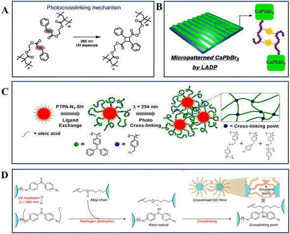 | ||
| Fig. 4 Photoreactive mechanisms and applications in direct optical lithography and nanomaterial hybridization. (A) Photo-cross-linking mechanism of the cinnamoyl group on the ligand during the patterning process (only the head-to-tail cycloaddition mechanism is presented for simplicity).43 Copyright 2021, American Chemical Society. (B) Graphical description of patterned CsPbBr3via ligand-assisted direct optical lithography.43 Copyright 2021, American Chemical Society. (C) Schematic illustration of hybridization of nanomaterials with PTPA-N3-SH ligands.50 Copyright 2021, the Royal Society of Chemistry. (D) Schematic illustrating the photocrosslinking between dual-ligand nanomaterials. On UV irradiation, the carbonyl group yields a radical and forms a covalent bond with the ligands of neighboring nanomaterials.45 Copyright 2022, Springer Nature. | ||
3.2 Patterning with photosensitive molecules as additives
The aforementioned patterning strategies are based on ligand photochemistry, where ligand changes affect the solubility or dissolution rate of the materials in specific solvents. Consequently, this process typically requires a pretreatment step before initiating patterning, in which pristine nanomaterials undergo ligand exchange with photosensitive ligands.92 However, recent research demonstrated a more streamlined approach that can bypass this pretreatment process. Direct optical lithography can be achieved by directly incorporating photo-induced additives into the nanomaterial film without the need for prior ligand exchange.The utilization of PAGs has enabled a significant advancement in high-resolution patterning. Upon UV irradiation, the PAG molecules were optically decomposed and protons were generated. The as-generated protons facilitated the detachment of the carboxylate surface ligands on the nanomaterials surface, thereby altering the solubility of the nanomaterials.38,49 As shown in Fig. 5A, a special ink containing nanomaterials (capped with carboxylates such as oleic acid) and PAGs (such as 2-(4-methoxystyryl)-4,6-bis(trichloromethyl)-1,3,5-triazine (MBT) and 2-diazo1-naphthol-4-sulfonic acid) was designed.52 Building upon this, other researchers have explored the use of photoamine generators (PAmGs) as additives, which decompose under deep UV exposure to release primary amines such as n-butylamine. Xiao et al. demonstrated that these released amines can bind to the exposed surface cations of nanomaterials, thereby reducing the solubility and forming uniform patterns (Fig. 5B).53
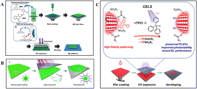 | ||
| Fig. 5 High-resolution nanoscale patterning strategy utilizing different additives in nanomaterial inks. (A) Schematic of the DOLFIN process using nanomaterial inks, highlighting the role of PAGs in UV-induced, high-resolution patterning of luminescent core/shell nanomaterials.52 Copyright 2020, Wiley-VCH GmbH. (B) Illustration of PAmG-assisted DOLFIN, showing the release of primary amines upon UV exposure, which bind to nanomaterial surfaces, reducing solubility and forming uniform patterns.53 Copyright 2023, The Author(s). (C) Schematic of light-triggered CELS, depicting TPCl photodissociation under 254 nm UV light into TP+ and Cl−. TP+ cations remove native surface ligands, enhancing pattern fidelity, while Cl− anions passivate the surface, preserving nanomaterial properties for stable patterning.47 Copyright 2023, American Chemical Society. | ||
Zhang et al. expanded the scope of direct photopatterning by proposing a method that incorporates photosensitive additives, such as triphenylmethyl chloride (TPCl), into nanomaterial films.47 TPCl underwent photodissociation, yielding triphenylcarbonium cations (TP+) and chloride anions (Cl−). As shown in Fig. 5C, the local release of the Lewis acidic TP+ cations effectively stripped the native ligands from the nanomaterial surface, reducing their solubility in nonpolar solvents and paving the way for high-resolution patterns.
The innovative approaches utilizing PAGs, PAmGs, and other photoactive additives have significantly advanced the field of direct photopatterning of nanomaterials. Furthermore, the application of compounds containing azide groups as photosensitive additives for nanomaterial patterning has further expanded the scope of this technology. Kang and colleagues pioneered the application of a phenyl azide-based photo-crosslinking agent, ethane-1,2-diyl bis(4-azido-2,3,5,6-tetrafluorobenzoate), as an additive for direct photopatterning of nanomaterials.54 This agent, known for its photoactivity, forms reactive nitrene intermediates upon UV exposure at 254 nm, which can readily engage in C–H insertion reactions with nearby alkyl chains (as depicted in Fig. 6A). This discovery facilitated a systematic investigation into how the structure of fluorinated aryl azide (the light-driven ligand crosslinkers, referred to as n-LiXers, are denoted with “n” indicating the number of azide units present in the molecule) relates to the structural and photophysical attributes of nanomaterial patterns, as shown in Fig. 6B.55 Zhang and colleagues reported the use of carbene-based crosslinkers for nanomaterial patterning for the first time, broadening the scope of direct optical patterning techniques.37,44 The general mechanism for this patterning process is outlined in Fig. 6C and D. Under UV irradiation, the photolysis of these crosslinker molecules releases nitrogen and generates highly reactive singlet nitrene or carbene intermediates. These intermediates are prone to undergo nonspecific C–H insertion with the native alkyl ligands of the nanomaterials, forming covalent bonds between adjacent nanomaterials. This crosslinking significantly diminishes the solubility of the nanomaterials in the exposed areas within their original nonpolar solvents, laying the groundwork for pattern formation.
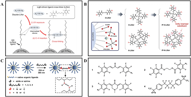 | ||
| Fig. 6 Direct optical patterning of QDs and NCs through photochemical crosslinking. (A) Schematic illustration of the ligand crosslinking process between adjacent QDs facilitated by the C–H insertion reaction of the nitrene moiety derived from the LiXer.54 Copyright 2020, The Author(s). The inset provides the chemical structure of ethane-1,2-diyl bis(4-azido-2,3,5,6-tetrafluorobenzoate), the specific LiXer utilized in this research. (B) Chemical structures of the series of n-LiXers and isopropyl-n-LiXers, highlighting the design variations that influence the crosslinking efficiency and photophysical properties of the resulting nanocrystal patterns.55 Copyright 2022, Wiley-VCH GmbH. (C) Patterning mechanism overview, depicting how photogenerated nitrene and carbene-based crosslinkers form covalent bonds with native ligands on neighboring NCs, enabling high-resolution pattern formation through C–H insertion reactions.37 Copyright 2024, American Chemical Society. (D) Molecular structures of four representative photocrosslinkers, emphasizing the distinct functional groups that contribute to the photochemical reactivity and patterning performance of the nanocrystals.44 Copyright 2022, Wiley-VCH GmbH. | ||
Additionally, the utilization of the thiol-ene click reaction for nanomaterial film patterning offers several distinct advantages. This innovative approach leverages the exceptional efficiency of the thiol-ene reaction to induce crosslinking between thiol molecules and the carbon double bonds present in the surface ligands of nanomaterials upon UV irradiation. The process is very efficient, allowing for precise patterning without the need for ligand exchange processes or the introduction of byproducts. Shin et al. used pentaerythritol tetrakis(3-mercaptopropionate) (PETMP) as a thiol additive for efficient cross-linking reactions with oleic acid ligands on the QD surface.57 Under UV light irradiation, these thiol molecules were made to react with the QD ligands containing C![[double bond, length as m-dash]](https://www.rsc.org/images/entities/char_e001.gif) C bonds to form thiyl radicals and cross-link them, resulting in microscale photo-patterning of QD films. This cross-linking strategy not only enhances the solvent resistance of the QD films, but also improves their optoelectronic properties.
C bonds to form thiyl radicals and cross-link them, resulting in microscale photo-patterning of QD films. This cross-linking strategy not only enhances the solvent resistance of the QD films, but also improves their optoelectronic properties.
The success of these strategies lies in their simplicity, universality, and the ability to preserve or even improve the intrinsic properties of a wide range of nanomaterials. This convergence of material chemistry and photochemistry opens up new horizons for the development of next-generation optoelectronic devices, including high-resolution displays and advanced integrated circuits, by enabling the precise and non-destructive patterning of nanomaterial films at a level of control that was previously unattainable.
3.3 Patterning without photosensitive molecules
The mechanism of direct optical lithography without photosensitizers marks a significant breakthrough in nanotechnology, offering a streamlined and practical approach to the fabrication of nanostructures. This method leverages the susceptibility of bare colloidal NCs to oxidation under UV irradiation. Through a photochemical oxidation process, the surface state of the NCs is altered, reducing their solubility in polar solvents. This change facilitates the creation of high-resolution patterns using a straightforward exposure and development process.83In their pioneering work, Pan et al. introduced a method for direct optical patterning that did not require photosensitive ligands or additives (Fig. 7).48 They utilized a strong acid, such as HBF4 in dimethylformamide (DMF), to strip the native ligands from the original nanomaterials, resulting in electrostatically stabilized “bare” nanomaterials. These “bare” nanomaterials were then deposited as thin films and selectively exposed to UV light through a photomask, inducing local photo-oxidation of surface atoms and triggering changes in solubility. The strategic combination of electrostatically stabilized bare nanomaterials with non-coordinating anions such as BF4−, along with the well-demonstrated phenomenon of light-induced oxidation of semiconductor nanomaterials, has led to the development of a novel ligand-free direct optical lithography technique.
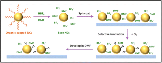 | ||
| Fig. 7 Schematic of ligand-free direct optical lithography for patterning bare colloidal NCs.48 The process initiates with the synthesis of NCs capped with organic ligands, which are then removed via ligand exchange using HBF4 in DMF, yielding electrostatically stabilized “bare” NCs. These NCs are deposited on a substrate and selectively irradiated through a photomask, inducing surface photo-oxidation and altering solubility. Development in DMF removes unexposed areas, resulting in a precisely patterned NC layer. This technique demonstrates high-resolution patterning capability without the need for additional photosensitive ligands or additives. Copyright 2022, American Chemical Society. | ||
The implications of this method were significant as it provided a direct and convenient patterning approach for a variety of NCs, including but not limited to ZnSe, CdSe, ZnS, InP, and CeO2.48,81,82 In addition, by employing auxiliary processing techniques such as using block copolymer templates and hot isostatic pressing, the porosity and refractive index of patterned films could be adjusted, further enhancing the versatility of this technology.84–86 This tunability is critical for advanced nanophotonic devices and applications that demand precise control over the physical and chemical properties of nanomaterials.
4 Selection of nanomaterials in direct optical lithography
The study of photopatternable nanomaterials is an important area at the intersection of materials science, nanotechnology and micro-nano manufacturing technology. These efforts directly determine the versatility and applicability of direct optical lithography techniques. In recent years, there has been growing interest among researchers in the diversity of materials suitable for direct optical lithography. In addition to the widely used QD materials, more emerging nanomaterials continue to be developed as direct patternable materials, such as metal oxides, metals, clusters, and MOFs. This section will provide an in-depth look at the various nanoscale materials that can be patterned directly using optical lithography.4.1 Parameters for evaluating pattern quality
Before investigating nanomaterials for direct optical lithography, it is crucial to define criteria and parameters for assessing the quality of patterning. This approach ensures that we can accurately measure and refine the patterning process, thereby enhancing the performance and reliability of the final device. The primary considerations include:- Resolution and pattern fidelity. The feature size determines the resolution or pixel density. High resolution means that more functional units can be accommodated in a small area, which is critical to improving device integration and performance. For example, in high-pixel-density displays, high-resolution lithography is essential for producing finer images and offering a sharper visual experience. Fidelity ensures that the optical and electronic properties of the nanomaterials remain intact during patterning. In QLEDs, the photoluminescence quantum yield (PLQY) and electroluminescence (EL) properties of the QDs must be preserved during the patterning process to ensure the color accuracy and brightness of the display.38,49
- Surface and edge quality. The line-edge roughness (LER) and line-width roughness (LWR) are critical metrics for the success of nanomaterial patterning. Low LER and LWR indicate that the pattern has well-defined edges and consistent line widths, which is essential for precise pixel alignment and color management. Poor LER and LWR mean that pattern edges are not sharp and line widths are not uniform, affecting the device's optical performance, such as brightness and color uniformity. They can also compromise electronic properties such as charge transport efficiency and device stability.13,34,93
- Device performance evaluation. One important criterion for evaluating the patterning quality of direct optical lithography is the performance of devices constructed using patterned nanomaterials. This comprehensive evaluation includes testing the devices' conductivity, optical efficiency, and long-term stability. For example, devices such as LEDs and photodetectors, which rely on patterned nanomaterials, require meticulous testing to ensure their effectiveness in practical applications.38,47,75
4.2 Luminescent materials – quantum dots (QDs)
When the size of semiconductor materials is precisely controlled within the range of 2 to 20 nm, the electronic and optical properties of these materials differ markedly from those of their three-dimensional bulk counterparts. QDs exhibit unique quantum confinement effects, with their bandgap being size-dependent, which reveals their tremendous potential in the field of optoelectronic conversion.94–96The exceptionally high PLQY and extremely narrow emission spectrum make QDs widely applicable in various optoelectronic devices, including LEDs, photodetectors, and laser devices. Particularly in the realm of LED displays, QDs not only significantly enhance color fidelity and image quality stability but also facilitate the precise alignment of pixels through direct optical lithography patterning technology, which is crucial for improving display resolution and visual performance.97–100 To fully harness the potential of QDs, researchers are actively exploring more efficient and precise synthesis and patterning techniques. By optimizing the synthesis process, it is possible to produce QDs that exhibit high consistency and stability. On the other hand, precise optical lithography techniques can be applied to directly pattern these QDs into specific locations, paving the way for the creation of complex light-emitting arrays or circuit configurations. These technological advancements are integrated to revolutionize the manufacturing of next-generation high-performance optoelectronic devices.
In recent years, the patterning technology of semiconductor QDs has undergone rapid development, with significant advances particularly evident in the areas of Cd-based QDs, green and non-toxic InP-based QDs, and perovskite nanocrystal (PNC)-based QDs. Talapin and his colleagues developed an innovative, high-resolution patterning technology that eliminates the need for a photoresist, particularly suitable for QLEDs based on Cd-based QDs.52 The team achieved high-quality synthesis of cadmium-based QDs by meticulously controlling the synthesis conditions and accomplished patterning through direct optical lithography with a feature size of approximately 1.5 μm, which is critical for high-resolution display technologies (Fig. 8A). In the patterning process, they utilized ultraviolet (UV) light with wavelengths of 365 or 405 nm as the light source, and the exposure dose was controlled by adjusting the duration of exposure while maintaining a power density of 30 mW cm−2. The resulting patterns feature high contrast with edge roughness estimated to be less than 50 nm, and the resolution achieved is 1.5 μm, meeting the demands of high-resolution display manufacturing.
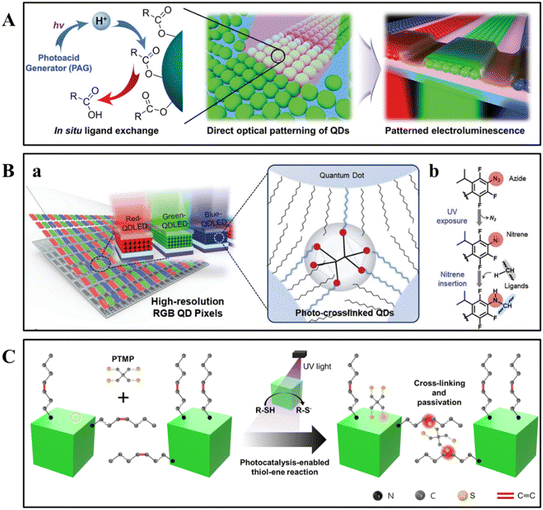 | ||
| Fig. 8 Schematic illustration of the patterning of QDs using direct optical lithography. (A) Schematic illustration of patterning using photochemically activated reactions between PAGs and the surface ligands of Cd-based QDs.52 Copyright 2020, Wiley-VCH GmbH. (B) Schematic illustration of photo-crosslinked heavy-metal-free QD patterns formed with branched n-LiXers (a) and the ligand crosslinking process (b).55 Copyright 2022, Wiley-VCH GmbH. (C) Schematic illustration of a process for patterning PNCs using photocatalysis through thiol-ene click chemistry.56 Copyright 2023, American Association for the Advancement of Science. | ||
Other researchers expanded the field by focusing on heavy-metal-free InP-based QDs, which were of interest due to their environmental friendliness and low toxicity.101–103 In their recent work, Kang et al. presented a groundbreaking approach to nondestructive direct photopatterning of heavy-metal-free InP-based QDs, leveraging branched LiXers (Fig. 8B).55 This technique achieved exceptional pattern resolution, with the ability to fabricate features as small as 1 μm, while maintaining the QDs' photoluminescence and EL properties. By employing a low UV dosage of 2 mJ cm−2 at 254 nm, the method ensured pattern fidelity and minimized edge roughness, which was pivotal for high-resolution display applications. The versatility of this approach across various QD types, provided they have compatible alkyl-ligand passivation, underscores its potential for broad implementation in the optoelectronic industry.
Furthermore, the research team investigated the patterning of PNCs. Himchan et al. presented a novel direct photocatalytic patterning method for PNCs and other luminescent nanomaterials, achieving high-resolution patterns without compromising the optical properties.56 The method leveraged a photoinduced thiol-ene click reaction, enabled by pentaerythritol tetrakis(3-mercaptopropionate) (PTMP), which also served as a defect passivation agent enhancing the PLQY by approximately 5% and photostability (Fig. 8C). Using a 275 nm light source, the patterning process was carried out at a low light intensity dose of approximately 30 millijoules per square centimeter. The PNCs exhibited high-resolution patterns with features as small as 560 nm, corresponding to a pixel density of over 12![[thin space (1/6-em)]](https://www.rsc.org/images/entities/char_2009.gif) 000 pixels per inch (ppi), and edge roughness measurements indicated a LWR of 0.6 μm and a LER of 0.22 μm, showcasing the potential for next-generation optoelectronic applications.
000 pixels per inch (ppi), and edge roughness measurements indicated a LWR of 0.6 μm and a LER of 0.22 μm, showcasing the potential for next-generation optoelectronic applications.
In summary, QDs have become the most widely used materials in photolithography due to their unique quantum confinement effects and size-dependent band gaps. Advances in direct optical patterning technology have led to significant advances in the patterning of Cd-based, InP-based and PNC-based QDs, not only improving pattern resolution but also maintaining the luminescent properties of the QDs, paving the way for the fabrication of high-performance optoelectronic devices.
4.3 Wide bandgap materials – metal oxides
Metal oxides possess high dielectric constants, transparency, and wide bandgaps in the UV to visible range, making them critical in electronic devices, photonics, and optoelectronic devices.104 These materials offer optical transparency, a high refractive index, and tunable conductivity, making them ideal candidates for high-performance device fabrication. It is notable that the implementation of high-resolution patterning is frequently a crucial step in optimizing the utilization of these properties and for seamlessly integrating oxide layers into practical device applications.Pan et al. utilized amorphous zirconia (ZrO2) nanoparticles for direct optical lithography, achieving micron-resolution patterns with a minimum feature size of 1.2 μm, as demonstrated in Fig. 9A.75 After annealing at 400 °C, the patterned ZrO2 layers demonstrated high diffraction behavior and excellent optical transparency across a wide wavelength range (0.3–10 μm). The patterning process involved irradiation with 405 nm light, which is widely available and compatible with standard photolithographic equipment. The exposure doses required for these amorphous ZrO2 nanoparticles were comparable to those used for commercial diazonaphthoquinone (DNQ) resists, with a minimum dose of less than 100 mJ cm−2 for a 500 nm thick film. After annealing at 400 °C, the patterned ZrO2 layers exhibited high diffraction behavior and excellent optical transparency across a wide wavelength range (0.3–10 μm). These layers possessed a high refractive index of approximately 1.84 at a wavelength of 633 nm, which is essential for fabricating high-performance optical components. Atomic force microscopy revealed an average surface roughness of 0.37 nm, ensuring minimal scattering loss and making these layers suitable for efficient optical applications.
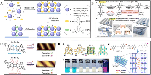 | ||
| Fig. 9 Schematic illustration of the patterning of QDs using direct optical lithography. (A) Schematic illustration of patterning using photochemically activated reactions between PAGs and the surface ligands of Cd-based QDs.75 Copyright 2021, American Chemical Society. (B) Schematic illustration of photo-crosslinked heavy-metal-free QD patterns formed with branched n-LiXers (a) and the ligand crosslinking process (b).105 Copyright 2022, American Chemical Society. (C) Schematic illustration of achieving patterning with different properties by adjusting the coordination structure of tin atoms and alkyl groups in tin–oxo clusters.106 Copyright 2024, Chinese Chemical Society. (D) Chemical principle of patterning MOFs through CLIP-MOF. (a) and (b) Schematic of colloidal MOF nanoparticles used as precursors for patterning. (c) Schematic of the crosslinking chemical reaction for patterning.41 Copyright 2024, The Author(s). | ||
Jeong and colleagues expanded the application of direct optical lithography by utilizing UV-induced cross-linking of zinc diacrylate (ZDA) to fabricate patterned ZnO thin films.107 They found that exposing the ZDA film to 254 nm ultraviolet light for 20 minutes resulted in clear patterns with micrometer resolution and feature spacings of less than 40 μm. The UV-irradiated ZDA thin films became insoluble in the developing solvent due to photo-cross-linking of the acrylate moiety. Atomic force microscopy (AFM) revealed that the patterned ZnO thin films had very smooth surfaces, with a root mean square (RMS) roughness value of 0.411 nm. This photocured ZnO film, created through direct optical lithography without the need for photoresists or additional photoinitiators, offers a novel approach for the production of thin-film transistors and complementary inverters operating at low voltages.
4.4 Conductive materials – metals
Metal nanomaterials play a critical role in nanotechnology due to their high conductivity, thermal conductivity, and unique surface plasmon resonance effects. These properties make them ideal candidates for sensors, optoelectronic devices, and catalytic applications. However, precise patterning is essential to integrate these materials into microscale and nanoscale electronic devices. This process allows for accurate control over material distribution at the microscopic level, which is crucial for the production of high-performance devices.38,47,49In the field of metal nanomaterial patterning, Wang and colleagues showed that the conductivity of gold nanocrystals can be significantly enhanced through a process that involves using the photoactive ligand NH4CS2N3 for patterning, followed by annealing at 150 °C.38 The resistivity of a 60 nm-thick gold film at 300 K, measured using the four-probe van der Pauw method, was found to be 5.2 × 10⁻⁸ ohm m. This value is comparable to that of gold films produced by physical vapor deposition highlighting the effectiveness of this method for the direct patterning of metal electrodes and interconnects.
Kwak and colleagues introduced a novel photopatterning method using the photocrosslinker 2Bx−4EO, which facilitates crosslinking reactions between silver nanowires (Ag NWs) and between Ag NWs and the substrate under UV irradiation at 254 nm (Fig. 9B).105 This process required only a minimal amount of the photo-crosslinker (<3 wt%), thus preserving the inherent physical properties of the Ag NW network. The resulting patterns had a resolution capable of achieving features as small as 10 μm, with an RMS roughness value of less than 6.5 nm, ensuring the maintenance of the network's excellent electrical characteristics. Additionally, by utilizing the roughness-assisted wetting phenomenon, poly(3,4-ethylenedioxythiophene)polystyrene sulfonate (PEDOT:PSS) was selectively coated onto the silver nanowire patterns, creating a bilayer nanowire/conducting polymer electrode.
4.5 Discrete molecular-like materials – clusters
Metal–organic clusters (MOCs) are a class of materials that consist of a metal or metal oxide core and peripheral organic ligands. They demonstrate considerable potential in the field of nanomanufacturing, particularly in advanced lithography techniques, due to their small size, excellent etch resistance, and high absorption efficiency for extreme ultraviolet (EUV) light.In their study, Peng and colleagues introduced a novel zinc–oxygen cluster molecule, Zn–VBA, which featured a [Zn4O]6+ core and six organic ligands based on 4-vinylbenzoic acid (VBA).108 The molecule displayed remarkable thermal stability, retaining its structure with only a 5% mass loss at 392 °C and maintaining integrity up to 400 °C, significantly outperforming reported zinc–oxo clusters with aliphatic acid ligands that typically have T95 (the temperature at which 5% weight loss is observed) below 200 °C. During e-beam lithography (EBL), Zn–VBA demonstrated a sensitivity of 20 μC cm−2 at an e-beam energy of 30 keV. Notably, at a dose of 5 μC cm−2, it was capable of producing patterns with 200 nm resolution. Moreover, atomic force microscopy (AFM) images revealed extremely low roughness values, underscoring Zn–VBA's potential for high-resolution patterning in advanced lithography applications.
Furthermore, two bicoordinated tin–oxo clusters, Sn4–Me–C10 and Sn4–Bu–C10, were investigated for their lithographic properties (Fig. 9C).106 In EBL, Sn4–Me–C10 demonstrated superior resolution, with an LER of 7.26 nm at an exposure dose of 640 μC cm−2. This characteristic was attributed to its higher Sn–C bond energy, which results in a lower propensity for free radical generation during exposure, thereby minimizing overexposure reactions and preserving the integrity of the patterned lines. Conversely, Sn4–Bu–C10 showcased greater sensitivity, with a dose-to-size (D0) of 4.05 μC cm−2 and a dose-to-insize (D100) of 123.94 μC cm−2. This higher sensitivity was primarily due to its lower Sn–C bond energy, which was more susceptible to cleavage under irradiation, leading to the generation of highly reactive species and enhancing photolithographic responsiveness. These results underscored the pivotal role of alkyl ligands in determining the irradiation chemistry and patterning performance of tin–oxo clusters in advanced lithography processes.
The click lithography technology proposed by He's research group was an innovative lithographic strategy that capitalizes on the high efficiency of the thiol-ene click reaction.39 Utilizing multialkene-functionalized ZrO2–methacrylic acid (MAA) clusters and thiol compounds, this approach achieved high-contrast patterning under an extremely low deep-ultraviolet exposure dose. The technology demonstrated a high sensitivity of 7.5 mJ cm−2 under DUV irradiation and enabled the creation of 45 nm dense patterns in e-beam lithography, highlighting its significant potential for high-resolution patterning. Then, they further reported the density functional theory (DFT) studies of the alkene-containing ZrO2 cluster, which are rationally synthesized accordingly, to disclose the mechanism of the nanoscale patterning driven by the switch of solubility from acid-catalyzed or electron-triggered ligand dissociation.109
4.6 Porous materials – metal–organic frameworks (MOFs)
Metal–organic frameworks (MOFs) are a versatile class of tunable porous materials, distinguished by their unique chemical properties, pore structures, and functionalities, making them ideal candidates for miniaturized solid-state devices with significant potential in integrated microelectronics and nanophotonics.41,110 Tian et al. introduced a patterning approach termed CLIP-MOF, which stands for crosslinking-induced patterning in MOFs. This innovative method utilizes resist-free direct photo- and electron-beam lithography for high-resolution patterning of diverse MOFs (Fig. 9D).41 This technique leveraged ligand cross-linking chemistry, where UV exposure at 254 nm with a dosage of 90 mJ cm−2 or electron-beam irradiation at a dosage of 50 μC cm−2 had activated the formation of covalent bonds on the surface of MOF nanoparticles. This activation resulted in an insoluble cross-linked network, significantly enhancing the solubility differential of MOFs in developer solvents and enabling selective dissolution of unexposed regions. The process achieved high-resolution patterning with a resolution of approximately 70 nm and edge roughness as low as 2.3 nm, suitable for both rigid and flexible substrates. The CLIP-MOF method was successfully applied to various MOFs, including ZIF-8, ZIF-7, HKUST-1, UiO-66, and Eu(BTC), preserving their crystallinity, porosity, and tailored functionalities. This approach demonstrated its potential as an efficient and versatile solution for direct patterning of MOF materials.5 Applications and device performance
The latest advancements in direct optical lithography have significantly enhanced the precision of nanomaterial patterning while preserving their critical optoelectronic properties, providing an accurate tool for micrometer-scale pixel patterning. Recent research has confirmed that efficient patterning can be achieved through direct optical lithography, successfully applied in the fabrication of advanced devices such as LEDs, transistors, diffraction gratings, and photodetectors. Moreover, the application of this technology in 3D printing and the patterning of upconversion nanoparticles (UCNPs) has further expanded its scope within the field of micro- and nanofabrication.5.1 QLEDs
In the field of QLED manufacturing, direct optical lithography patterning has become essential for fabricating high-resolution displays by precisely controlling the patterning of QDs.Zhang's team has achieved a breakthrough in the field of QLEDs by creating the highest-performing patterned cadmium-based QLEDs, setting a new benchmark.47 By employing direct optical patterning technology, they successfully developed QLEDs with high efficiency and long lifetimes (Fig. 10A). This method preserved the high PLQYs of the QDs and significantly improved their photostability. The resulting red, green, and blue QLEDs exhibited outstanding external quantum efficiencies (EQEs) of 19.1%, 17.5%, and 12.0% respectively. Moreover, at a brightness of 1000 nits, the T95 operational lifetimes of these devices were an impressive 7600 hours, 8700 hours, and 60 hours, respectively. These performance metrics were unprecedented for patterned QLEDs and comparable to those of non-patterned QLEDs.
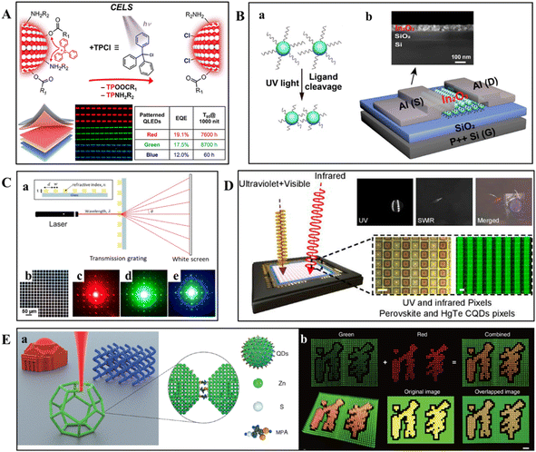 | ||
| Fig. 10 Schematic representation of the devices and their performance characteristics achieved by the direct photolithographic patterning process. (A) Schematic diagram of Cd-based QLEDs with high efficiency and long lifespan developed through direct optical lithography patterning using the light-triggered CELS technique.47 Copyright 2023, American Chemical Society. (B) Schematic illustration of the DOVE patterning process (a) and schematic illustration (bottom) and (b) SEM cross-section image (top) of TFTs with patterned In2O3 NC channels.78 Copyright 2022, American Chemical Society. (C) Schematic diagram of the diffraction grating scheme (a) constructed after patterning CeO2 NCs (note: figures are not drawn to scale). (b) Optical microscopy images of CeO2 NCs in a 2D pattern. (c)–(e) Diffraction patterns obtained by illuminating 2D grating patterns with red, green, and blue continuous-wave (CW) lasers.49 Copyright 2019, American Chemical Society. (D) Schematic diagram of a multispectral broadband CMOS-compatible imager implemented through layer-by-layer direct optical lithography of CQDs, featuring ultraviolet-enhanced visible pixels and SWIR pixels.79 Copyright 2022, American Chemical Society. (E) Schematic illustration showing 3D nanoprinting of 3-mercaptopropionic acid (MPA)-capped CdSe/ZnS QDs using PEB (a) and illustrating the multicolor display and heterogeneous 3D printing capabilities of the PEB technique, demonstrating the printing of “Tsinghua University” in yellow emitted light from a mixture of green and red QDs (b).111 Copyright 2022, American Association for the Advancement of Science. | ||
In another significant contribution, Oh and colleagues employed a thiol-ene click chemistry to pattern QDs.57 This strategy offers advantages such as rapid reaction kinetics, regioselectivity, and the ability to alter QD solubility without the need for additional photoinitiators. These characteristics not only greatly enhanced the chemical stability and solvent resistance of the QD films but also preserved their excellent optoelectronic properties. Notably, this crosslinking method increased the PLQY of QD films by 22.9%. Furthermore, in EL device testing, t the crosslinked QLEDs demonstrated a maximum brightness of 8463 cd m−2 and a peak current efficiency (CE) of 23.04 cd A−1, representing a 158% improvement over traditional InP QLEDs.
Regarding PNC-based QDs, researchers have successfully achieved non-destructive direct optical patterning of PNCs through the use of a well-designed carbon-based crosslinker.37 The resulting patterned LED device prototype exhibited a peak brightness of up to 64![[thin space (1/6-em)]](https://www.rsc.org/images/entities/char_2009.gif) 726 cd m−2 and a maximum EQE of approximately 16%, marking high-performance achievements among patterned perovskite LEDs.
726 cd m−2 and a maximum EQE of approximately 16%, marking high-performance achievements among patterned perovskite LEDs.
These breakthroughs advance the field of QD patterning technology, providing a solid foundation for the development of next-generation QLEDs. These future QLEDs are expected to be more efficient, stable, and capable of delivering vivid and long-lasting display performance.
5.2 Transistors
This technology also exhibits considerable promise in the fabrication of transistors, offering effective solutions for the miniaturization and efficiency of electronic devices, which is crucial for the advancement of integrated circuits and microchip technology.Wang and colleagues showed that the use of PAGs and NH4CS2N3 as surface ligands enables direct optical patterning of inorganic materials without compromising their electronic and optical properties.38 Specifically, in the fabrication of FETs, the patterning of CdSe NCs with a (p-CH3S–C6H4)(C6H5)2S+OTf− PAG, combined with compositionally matched Cd2Se32− semiconductor solders, has achieved an electron mobility (μe) of over 100 cm2 V−1 s−1. This represents a significant performance improvement attributed to optimized charge transport.
Furthermore, Wang and colleagues reported a direct optical patterning method for In2O3 NCs without the need for photosensitizing molecules, termed DOVE (Direct Optical UV Etching) technology (Fig. 10B).78 This technique leverages the cleavage of native ligands on In2O3 NCs under UV light exposure to achieve patterning. The thin-film transistors (TFTs) obtained through the DOVE process transitioned from an inactive to an active state, exhibiting substantially enhanced electronic performance following ligand exchange, with a saturation electron mobility (μsat) of 0.0005 cm2 V−1 s−1, a threshold voltage (Vth) of 1.6 V, a subthreshold swing (SS) of 1.3 V dec−1, and an on/off current ratio (Ion/off) of 1.6 × 10³.
These studies not only showcase the application potential of direct optical lithography in patterning inorganic materials but also provide new directions and possibilities for the future development of electronic devices.
5.3 Others
Direct optical lithography technology has expanded its applications to other areas in the field of nanomaterial patterning, with various innovative applications being reported.Direct optical lithography technology opened new avenues for the fabrication of optical components such as diffraction gratings, which are indispensable in optical communication systems and precision laser devices. In the study conducted by Wang et al., the potential of direct optical lithography was harnessed to pattern metal oxide materials efficiently.49 The process involved utilizing high refractive index materials to etch periodic patterns onto glass substrates, resulting in the creation of fully transparent binary phase diffraction grating prototypes (Fig. 10C). The gratings produced through one or two steps of direct optical lithography exhibited remarkable optical transparency and thermal stability, with the latter being tested up to 600 °C. These prototypes, with their exceptional optical and thermal properties, simplified the production process by eliminating the need for traditional photolithography steps, such as photoresist application and chemical etching, marking a significant breakthrough in fabrication techniques.
Pan et al. successfully patterned CsPbBr3 QDs on gold electrodes using direct optical lithography and a photo-induced ligand breakage mechanism to prepare photodetectors with excellent performance.73 These detectors had a significant photocurrent response to 395 nm UV irradiation and exhibited high sensitivity and fast response. In addition, a high quantum yield of 79% was achieved by ligand exchange treatment. Through ligand and anion exchange, the emission wavelength of the detectors could be tuned to cover the visible spectrum, broadening their spectral response range.
In addition, the Tang group constructed a colloidal quantum dot (CQD)-based multispectral broadband complementary metal oxide semiconductor (CMOS)-compatible photodetectors using direct optical lithography (Fig. 10D).79 The precise control provided by direct optical lithography enables the high-resolution imaging capabilities of the device and allowed for the integration of different spectral responses into a single unit. The detector captures a spectrum ranging from UV to short-wave infrared (SWIR) by utilizing UV-enhanced visible pixels and SWIR pixels. Its performance advantages include a photoresponse uniformity of less than 5%, no dead pixels, and room-temperature responsivities of 0.25 A W−1 at 300 nm, 0.4 A W−1 at 750 nm, and 0.25 A W−1 at 2.0 μm, which hold significant research value for applications such as fingerprint recognition, night vision, and material composition analysis.
In another study, Pan developed a method for directly patterning UCNPs that takes advantage of specifically designed ligands capable of forming new ionic or covalent bonds under UV, e-beam, or near-infrared (NIR) light exposure, achieving a patterning resolution as low as approximately 100 nm.112 This technique is crucial for applications in microscopy, sensing, and photonics, where extremely high-resolution patterning is required. The study demonstrated that 6 nm UCNPs could be patterned with compact ionic-based ligands, while larger UCNPs required long-chain, cross-linkable ligands to prevent irreversible aggregation. The researchers also emphasized the cost-effectiveness of continuous-wave lasers in high-resolution 2D and 3D lithography of colloidal materials, paving the way for next-generation UCNP applications in nonlinear photonics.
Recently, the research by Liu et al. has brought a new perspective to the field by presenting a 3D nanoprinting method using photoexcitation-induced chemical bonding (PEB) to create high-resolution structures from semiconductor QDs.111 The process involved the generation of electron–hole pairs under laser excitation, which led to the desorption of surface ligands and the formation of interparticle chemical bonds. The researchers demonstrated the technique by printing complex 3D structures, such as the characters for “Tsinghua University,” with a resolution exceeding the diffraction limit (Fig. 10E). The printed structures exhibited uniform height and fluorescence intensity distribution, with a minimum feature size of 81 ± 4 nm and a line edge roughness of 12 ± 2 nm. The photoluminescence (PL) spectra and radiative recombination lifetimes of the printed QDs were comparable to those of the original QD dispersions, indicating that the PEB process preserves the optoelectronic properties of the QDs.
Direct optical lithography represents a pivotal technology in the field of optoelectronics, offering the capability to pattern materials with precision while maintaining their intrinsic properties. It plays an important role in enhancing display resolution, device performance, and reducing costs. It will expand its applications as it progresses, addressing industry demands for complexity and miniaturization.
6 Summary and perspectives
In this review, we comprehensively reviewed pattern design strategies and their related mechanisms in direct optical lithography, with a particular focus on QDs and other advanced nanomaterials, such as metal oxides, metals, clusters, and MOFs. This article provides insights into the advantages of these materials in the patterning process, as well as their unique properties in forming high-resolution patterns. In addition, we summarized the applications of these materials in the fabrication of high-resolution display screens, high-sensitive photodetectors, and high-performance light-emitting diodes, highlighting the versatility and significant value of direct optical lithography technology in the field of nanofabrication.As technology continues to advance, photolithography is evolving towards higher resolution, greater flexibility and greater environmental adaptability. It is expected that increasingly complex micro- and nanostructures will be realized through direct optical lithography in the future, thereby meeting the stringent requirements of nanoscale manufacturing and facilitating innovation in a range of fields, including microelectronics, optoelectronics, biomedicine and new materials. However, the field is still in the developmental stage and requires further research and exploration, particularly in the following areas:
6.1 Developing direct patterning for multilevel complex structures
Multilevel direct patterning technology represents a significant advancement from traditional planar lithographic processes, proposed to meet the increasing demand for micro- and nanostructures beyond two dimensions, such as 2.5D and 3D. Recent studies have reported the realization of 2.5D and 3D printing through the photochemical bonding of QDs.113,114 This technology's ability to handle a variety of materials and create complex 3D structures paves the way for a new era in manufacturing. As it continues to mature, it is expected to play a crucial role in driving innovation and enabling the development of next-generation devices and systems with unprecedented performance and functionality.6.2 Advancing EUV lithography with metal-based inorganic materials
The current trend in photolithography is towards ultraviolet to visible wavelengths to meet practical application needs, but short wavelength patterning, particularly in EUV lithography, remains critical. Traditional organic photoresists, well established for DUV lithography, face significant challenges when applied to EUV lithography, such as diminished sensitivity and inadequate etch resistance.115–117 In contrast, metal-based inorganic materials, with their d-orbital electrons, provide an EUV absorption cross-section many times larger than that of carbon, effectively mitigating the reduced photosensitivity due to the failure of chemical amplification mechanisms. In addition, these materials offer superior etch resistance compared to their organic counterparts, enabling higher line densities and aspect ratios essential for the manufacture of more integrated advanced chips.118,119 Thus, metal- or semiconductor-based inorganic nanoparticles with high resolution, etch resistance and EUV absorption coefficients are a potential solution to the existing problems in EUV lithography, making them suitable for direct EUV patterning.6.3 Environmentally friendly systems
In the future, the development of direct optical lithography technology will increasingly favor the use of environmentally friendly nanomaterials and processes to achieve green manufacturing. It is important to explore more efficient lithography processes to minimize chemical waste and wastewater emissions during production. Consequently, the use of industrial green solvents, such as propylene glycol methyl ether acetate (PGMEA) and diethylene glycol ether acetate (DGMEA), for patterning will be a key direction in the future evolution of direct optical lithography technology.In conclusion, the development of direct optical lithography technology will significantly accelerate the process of constructing complex nanomaterial-based devices at the nanoscale using solution-based methods. Its compatibility with various nanomaterials and substrates offers new pathways for developing diverse hybrid devices.
List of abbreviations
| AFM | Atomic force microscopy |
| Ag NWs | Silver nanowires |
| Cat+ | Cationic |
| CE | Current efficiency |
| Cl− | Chloride anions |
| CLIP-MOF | Crosslinking-induced patterning in MOFs |
| CMOS | Complementary metal oxide semiconductor |
| CQDs | Colloidal quantum dots |
| DFT | Density functional theory |
| DGMEA | Diethylene glycol ether acetate |
| DMF | Dimethylformamide |
| DNQ | Diazonaphthoquinone |
| DOLFIN | Direct optical lithography of functional inorganic nanomaterials |
| DOVE | Direct optical UV etching |
| DUV | Deep ultraviolet |
| e-beam | Electron beam |
| EBL | e-beam lithography |
| EL | Electroluminescence |
| EOC | A highly transparent negative overcoat photoresist |
| EQEs | External quantum efficiencies |
| EUV | Extreme ultraviolet |
| FETs | Field-effect transistors |
| I on/off | On/off current ratio |
| LEDs | Light-emitting diodes |
| LER | Line-edge roughness |
| LWR | Line-width roughness |
| MAA | Multialkene-functionalized ZrO2–methacrylic acid |
| MOCs | Metal–organic clusters |
| MOFs | Metal–organic frameworks |
| MPA | 3-Mercaptopropionic acid |
| NCs | Nanocrystals |
| NH4CS2N3 | Ammonium 1,2,3,4-thiatriazole-5-thiolate |
| NIR | Near-infrared |
| n-LiXers | The light-driven ligand crosslinkers, “n” represents the number of azide groups in the molecule |
| PAGs | Photoacid generators |
| PAmGs | Photoamine generators |
| PEB | Photoexcitation-induced chemical bonding |
| PEDOT:PSS | Poly(3,4-ethylenedioxythiophene)polystyrene sulfonate |
| PETMP | Pentaerythritol tetrakis(3-mercaptopropionate) |
| PGMEA | Propylene glycol methyl ether acetate |
| Ph2I+ | Diphenyliodonium cations |
| Ph3S+ | Triphenylsulfonium cations |
| PL | Photoluminescence |
| PLQY | Photoluminescence quantum yield |
| PNCs | Perovskite nanocrystals |
| QDs | Quantum dots |
| QLEDs | Quantum dot light-emitting diodes |
| RMS | Root mean square |
| SS | Subthreshold swing |
| SU-8 | A photoreactive bisphenol A-based epoxy resin |
| SWIR | Short-wave infrared |
| TFTs | Thin-film transistors |
| TP+ | Triphenylcarbonium cations |
| TPCl | Triphenylmethyl chloride |
| t-SPL | Thermal scanning probe lithography |
| TTT | Ammonium 1,2,3,4-thiatriazole-5-thiolate |
| UCNPs | Upconversion nanoparticles |
| UV | Ultraviolet |
| VBA | 4-Vinylbenzoic acid |
| V th | Threshold voltage |
| X− | Active anionic |
| ZDA | Zinc diacrylate |
| μ e | Electron mobility |
| μ sat | Saturation electron mobility |
Data availability
No primary research results, software or code have been included and no new data were generated or analyzed as part of this review.Author contributions
Yuelin Yang: data curation, writing – original draft, writing – review & editing. Jie Guan: data curation, writing – original draft. Nannan Zhang: conceptualization, writing – review & editing. Lin Ru: conceptualization, writing – review & editing. Yihao Zou: conceptualization, writing – review & editing. Yuanyuan Wang: conceptualization, supervision, writing – review & editing, funding acquisition.Conflicts of interest
The authors declare no conflict of interest.Acknowledgements
This work was supported by the National Key R&D Program of China (2022YFB3607000), the Science and Technology Program in Jiangsu Province (BK20232041), the National Natural Science Foundation of China (22171132 and 52472165), the Program for Innovative Talents and Entrepreneurs in Jiangsu (020513006012 and 020513006014) and the Zijin Scholars Foundation (0205181022).References
- M. M. El-Kady, I. Ansari, C. Arora, N. Rai, S. Soni, D. K. Verma, P. Singh and A. E. D. Mahmoud, J. Mol. Liq., 2023, 370, 121046 CrossRef CAS.
- B. Mekuye and B. Abera, Nano Sel., 2023, 4, 486–501 CrossRef CAS.
- R. Augustine, A. A. Mamun, A. Hasan, S. A. Salam, R. Chandrasekaran, R. Ahmed and A. S. Thakor, Adv. Colloid Interface Sci., 2021, 294, 102457 CrossRef CAS PubMed.
- Y. V. Lee and B. Tian, Nano Lett., 2019, 19, 2189–2197 CrossRef CAS PubMed.
- P. L. Saldanha, V. Lesnyak and L. Manna, Nano Today, 2017, 12, 46–63 CrossRef CAS.
- M. V. Kovalenko, L. Manna, A. Cabot, Z. Hens, D. V. Talapin, C. R. Kagan, V. I. Klimov, A. L. Rogach, P. Reiss, D. J. Milliron, P. Guyot-Sionnnest, G. Konstantatos, W. J. Parak, T. Hyeon, B. A. Korgel, C. B. Murray and W. Heiss, ACS Nano, 2015, 9, 1012–1057 CrossRef CAS PubMed.
- X. Cui, Q. Ruan, X. Zhuo, X. Xia, J. Hu, R. Fu, Y. Li, J. Wang and H. Xu, Chem. Rev., 2023, 123, 6891–6952 CrossRef CAS PubMed.
- C. A. Ferreira, D. Ni, Z. T. Rosenkrans and W. Cai, Angew. Chem., Int. Ed., 2019, 58, 13232–13252 CrossRef CAS PubMed.
- S. Su, Q. Sun, X. Gu, Y. Xu, J. Shen, D. Zhu, J. Chao, C. Fan and L. Wang, TrAC, Trends Anal. Chem., 2019, 119, 115610 CrossRef CAS.
- X. Zhao, H. Jin, J. Liu, J. Chao, T. Liu, H. Zhang, G. Wang, W. Lyu, S. Wageh, O. A. Al-Hartomy, A. G. Al-Sehemi, B. Fu and H. Zhang, Laser Photonics Rev., 2022, 16, 2200386 CrossRef.
- J. Zhu and M. C. Hersam, Adv. Mater., 2017, 29, 1603895 CrossRef.
- Y. Xia, J. A. Rogers, K. E. Paul and G. M. Whitesides, Chem. Rev., 1999, 99, 1823–1848 CrossRef CAS PubMed.
- S. Y. Park, S. Lee, J. Yang and M. S. Kang, Adv. Mater., 2023, 35, e2300546 CrossRef PubMed.
- W. Guo, J. Chen, T. Ma, Z. Chen, M. Li, H. Zeng and J. Lu, Adv. Funct. Mater., 2023, 34, 2310338 CrossRef.
- S. Baek and J. S. Son, Adv. Phys. Res., 2023, 3, 2300069 CrossRef.
- M. S. M. Saifullah, M. Asbahi, M. Binti-Kamran Kiyani, S. Tripathy, E. A. H. Ong, A. Ibn Saifullah, H. R. Tan, T. Dutta, R. Ganesan, S. Valiyaveettil and K. S. L. Chong, ACS Nano, 2017, 11, 9920–9929 CrossRef CAS PubMed.
- M. S. M. Saifullah, M. Asbahi, D. C. J. Neo, Z. Mahfoud, H. R. Tan, S. T. Ha, N. Dwivedi, T. Dutta, S. Bin Dolmanan, Z. Aabdin, M. Bosman, R. Ganesan, S. Tripathy, D. G. Hasko and S. Valiyaveettil, Nano Lett., 2022, 22, 7432–7440 CrossRef CAS PubMed.
- D. Zhou, P. Zhao, J. Zhang, X. Jiang, S. Qin, X. Zhang, R. Jiang, Y. Deng, H. Jiang, G. Zhan, Y. Luo, H. Ma and L. Wang, Small, 2022, 18, e2205227 CrossRef PubMed.
- H. Wu, Y. Wang, J. Yu, J. A. Pan, H. Cho, A. Gupta, I. Coropceanu, C. Zhou, J. Park and D. V. Talapin, J. Am. Chem. Soc., 2022, 144, 10495–10506 CrossRef CAS PubMed.
- G. W. Yang, G. P. Wu, X. Chen, S. Xiong, C. G. Arges, S. Ji, P. F. Nealey, X. B. Lu, D. J. Darensbourg and Z. K. Xu, Nano Lett., 2017, 17, 1233–1239 CrossRef CAS PubMed.
- F. Li, C. Chen, S. Lu, X. Chen, W. Liu, K. Weng, Z. Fu, D. Liu, L. Zhang, H. Abudukeremu, L. Lin, Y. Wang, M. Zhong, H. Zhang and J. Li, ACS Nano, 2022, 16, 13674–13683 CrossRef CAS.
- W. Li, Y. Wang, M. Li, L. P. Garbarini and F. G. Omenetto, Adv. Mater., 2019, 31, e1901036 CrossRef PubMed.
- C. Wei, W. Su, J. Li, B. Xu, Q. Shan, Y. Wu, F. Zhang, M. Luo, H. Xiang, Z. Cui and H. Zeng, Adv. Mater., 2022, 34, e2107798 CrossRef PubMed.
- J. Cai, W. Lai, Y. Chen, X. Zhang, Y. Zheng, W. Zhang, X. Chen, Y. Ye, S. Xu, Q. Yan, T. Guo and E. Chen, Laser Photonics Rev., 2024, 2400298 CrossRef CAS.
- S. Y. Kim, J. I. Kwon, H. H. Song, G. H. Lee, W. S. Yu, S. Li, M. K. Choi and J. Yang, Appl. Surf. Sci., 2023, 610, 155579 CrossRef CAS.
- T. W. Nam, M. Kim, Y. Wang, G. Y. Kim, W. Choi, H. Lim, K. M. Song, M. J. Choi, D. Y. Jeon, J. C. Grossman and Y. S. Jung, Nat. Commun., 2020, 11, 3040 CrossRef CAS PubMed.
- T. Meng, Y. Zheng, D. Zhao, H. Hu, Y. Zhu, Z. Xu, S. Ju, J. Jing, X. Chen, H. Gao, K. Yang, T. Guo, F. Li, J. Fan and L. Qian, Nat. Photonics, 2022, 16, 297–303 CrossRef CAS.
- C. Zhu, H. Ekinci, A. Pan, B. Cui and X. Zhu, Microsyst. Nanoeng., 2024, 10, 52 CrossRef CAS.
- Y. Chen, Microelectron. Eng., 2015, 135, 57–72 CrossRef CAS.
- S. T. Howell, A. Grushina, F. Holzner and J. Brugger, Microsyst. Nanoeng., 2020, 6, 21 CrossRef.
- P. C. Paul, A. W. Knoll, F. Holzner, M. Despont and U. Duerig, Nanotechnology, 2011, 22, 275306 CrossRef PubMed.
- T. Cao, Z. Yang, H. Zhang and Y. Wang, Heliyon, 2024, 10, e30163 CrossRef CAS PubMed.
- J. Chen, K. Zhang, K. Zhang, L. Yang and B. Jiang, J. Appl. Polym. Sci., 2021, 138, e50894 CrossRef.
- X. Kong, X. Fan, Y. Wang, Y. Luo, Y. Chen, T. Wu, Z. Chen, Y. Lin and S. Wang, Nano Mater. Sci., 2024 DOI:10.1016/j.nanoms.2024.03.005.
- C. Luo, C. Xu, L. Lv, H. Li, X. Huang and W. Liu, RSC Adv., 2020, 10, 8385–8395 RSC.
- W. Khuen Ho, A. Tay, L. Lay Lee and C. D. Schaper, Control Engineering Practice, 2004, 12, 881–892 CrossRef.
- D. Liu, K. Weng, H. Zhao, S. Wang, H. Qiu, X. Luo, S. Lu, L. Duan, S. Bai, H. Zhang and J. Li, ACS Nano, 2024, 18, 6896–6907 CrossRef CAS PubMed.
- Y. Wang, I. Fedin, H. Zhang and D. V. Talapin, Science, 2017, 357, 385–388 CrossRef CAS PubMed.
- Q. Wang, H. Cui, X. Wang, Z. Hu, P. Tao, M. Li, J. Wang, Y. Tang, H. Xu and X. He, J. Am. Chem. Soc., 2023, 145, 3064–3074 CrossRef CAS PubMed.
- N. Li, Z. G. Gu and J. Zhang, Small Methods, 2023, 7, e2201231 CrossRef PubMed.
- X. Tian, F. Li, Z. Tang, S. Wang, K. Weng, D. Liu, S. Lu, W. Liu, Z. Fu, W. Li, H. Qiu, M. Tu, H. Zhang and J. Li, Nat. Commun., 2024, 15, 2920 CrossRef CAS PubMed.
- J. Lee, J. Ha, H. Lee, H. Cho, D. C. Lee, D. V. Talapin and H. Cho, ACS Energy Lett., 2023, 8, 4210–4217 CrossRef CAS.
- J. Ko, K. Ma, J. F. Joung, S. Park and J. Bang, Nano Lett., 2021, 21, 2288–2295 CrossRef CAS PubMed.
- S. Lu, Z. Fu, F. Li, K. Weng, L. Zhou, L. Zhang, Y. Yang, H. Qiu, D. Liu, W. Qing, H. Ding, X. Sheng, M. Chen, X. Tang, L. Duan, W. Liu, L. Wu, Y. Yang, H. Zhang and J. Li, Angew. Chem., Int. Ed., 2022, 61, e202202633 CrossRef CAS PubMed.
- D. Hahm, J. Lim, H. Kim, J. W. Shin, S. Hwang, S. Rhee, J. H. Chang, J. Yang, C. H. Lim, H. Jo, B. Choi, N. S. Cho, Y. S. Park, D. C. Lee, E. Hwang, S. Chung, C. M. Kang, M. S. Kang and W. K. Bae, Nat. Nanotechnol., 2022, 17, 952–958 CrossRef CAS PubMed.
- L. Dan, W. Kangkang, L. Shaoyong, L. Fu, A. Hannikezi, Z. Lipeng, Y. Yuchen, H. Junyang, Q. Hengwei, F. Zhong, L. Xiyu, D. Lian, Z. Youyu, Z. Hao and L. Jinghong, Sci. Adv., 2022, 8, eabm8433 CrossRef PubMed.
- Z. Fu, L. Zhou, Y. Yin, K. Weng, F. Li, S. Lu, D. Liu, W. Liu, L. Wu, Y. Yang, H. Li, L. Duan, H. Xiao, H. Zhang and J. Li, Nano Lett., 2023, 23, 2000–2008 CrossRef CAS PubMed.
- J. A. Pan, H. Wu, A. Gomez, J. C. Ondry, J. Portner, W. Cho, A. Hinkle, D. Wang and D. V. Talapin, ACS Nano, 2022, 16, 16067–16076 CrossRef CAS PubMed.
- Y. Wang, J. A. Pan, H. Wu and D. V. Talapin, ACS Nano, 2019, 13, 13917–13931 CrossRef CAS PubMed.
- B. M. Oh, Y. Jeong, J. Zheng, N. Y. Cho, M. Song, J. W. Choi and J. H. Kim, Chem. Commun., 2021, 57, 12824–12827 RSC.
- J. Ko, J. H. Chang, B. G. Jeong, H. J. Kim, J. F. Joung, S. Park, D. H. Choi, W. K. Bae and J. Bang, ACS Appl. Mater. Interfaces, 2020, 12, 42153–42160 CrossRef PubMed.
- H. Cho, J. A. Pan, H. Wu, X. Lan, I. Coropceanu, Y. Wang, W. Cho, E. A. Hill, J. S. Anderson and D. V. Talapin, Adv. Mater., 2020, 32, e2003805 CrossRef PubMed.
- P. Xiao, Z. Zhang, J. Ge, Y. Deng, X. Chen, J. R. Zhang, Z. Deng, Y. Kambe, D. V. Talapin and Y. Wang, Nat. Commun., 2023, 14, 49 CrossRef CAS PubMed.
- J. Yang, D. Hahm, K. Kim, S. Rhee, M. Lee, S. Kim, J. H. Chang, H. W. Park, J. Lim, M. Lee, H. Kim, J. Bang, H. Ahn, J. H. Cho, J. Kwak, B. Kim, C. Lee, W. K. Bae and M. S. Kang, Nat. Commun., 2020, 11, 2874 CrossRef CAS PubMed.
- J. Yang, M. Lee, S. Y. Park, M. Park, J. Kim, N. Sitapure, D. Hahm, S. Rhee, D. Lee, H. Jo, Y. H. Jo, J. Lim, J. Kim, T. J. Shin, D. C. Lee, K. Kwak, J. S. Kwon, B. Kim, W. K. Bae and M. S. Kang, Adv. Mater., 2022, 34, e2205504 CrossRef PubMed.
- M. Seongkyu, P. S. Jae, L. Jaehwan, L. Hyungdoh, C. Jonghui, K. J. Ku and C. Himchan, Sci. Adv., 2023, 9, eadi6950 CrossRef PubMed.
- S. Shin, K. Kang, H. Jang, N. Gwak, S. Kim, T. A. Kim and N. Oh, Small Methods, 2023, 7, e2300206 CrossRef PubMed.
- P. Zhang, G. Yang, F. Li, J. Shi and H. Zhong, Nat. Commun., 2022, 13, 6713 CrossRef CAS PubMed.
- A. G. Shulga, A. Yamamura, K. Tsuzuku, R. M. Dragoman, D. N. Dirin, S. Watanabe, M. V. Kovalenko, J. Takeya and M. A. Loi, Adv. Mater. Technol., 2019, 4, 1900054 CrossRef CAS.
- C. Ingrosso, V. Fakhfouri, M. Striccoli, A. Agostiano, A. Voigt, G. Gruetzner, M. L. Curri and J. Brugger, Adv. Funct. Mater., 2007, 17, 2009–2017 CrossRef CAS.
- S. Lee, Polymer, 2019, 182, 121839 CrossRef CAS.
- V. M. Menon, S. Husaini, N. Okoye and N. V. Valappil, J. Nanophotonics, 2009, 3, 031608 CrossRef.
- S. Srivastava, K. E. Lee, E. A. Fitzgerald, S. J. Pennycook and S. Gradecak, ACS Appl. Mater. Interfaces, 2022, 14, 48995–49002 CrossRef CAS PubMed.
- J. Jang, Y. H. Kim, S. Park, D. Yoo, H. Cho, J. Jang, H. B. Jeong, H. Lee, J. M. Yuk, C. B. Park, D. Y. Jeon, Y. H. Kim, B. S. Bae and T. W. Lee, Adv. Mater., 2021, 33, e2005255 CrossRef PubMed.
- S.-W. H. Chen, Y.-M. Huang, K. J. Singh, Y.-C. Hsu, F.-J. Liou, J. Song, J. Choi, P.-T. Lee, C.-C. Lin, Z. Chen, J. Han, T. Wu and H.-C. Kuo, Photonics Res., 2020, 8, 630–636 CrossRef CAS.
- P. Li, X. Zhang, Y. Li, L. Qi, C. W. Tang and K. M. Lau, J. Soc. Inf. Disp., 2020, 29, 157–165 CrossRef.
- S. Lee and C. Lee, Polym. Adv. Technol., 2018, 30, 749–754 CrossRef.
- X. Li, D. Kundaliya, Z. J. Tan, M. Anc and N. X. Fang, Opt. Express, 2019, 27, 30864–30874 CrossRef CAS PubMed.
- Y. H. Kim, S. Koh, H. Lee, S. M. Kang, D. C. Lee and B. S. Bae, ACS Appl. Mater. Interfaces, 2020, 12, 3961–3968 CrossRef CAS PubMed.
- Y. Nakanishi, T. Takeshita, Y. Qu, H. Imabayashi, S. Okamoto, H. Utsumi, M. Kanehiro, E. Angioni, E. A. Boardman, I. Hamilton, A. Zampetti, V. Berryman-Bousquet, T. M. Smeeton and T. Ishida, J. Soc. Inf. Disp., 2020, 28, 499–508 CrossRef CAS.
- D. Hahm, J. Park, I. Jeong, S. Rhee, T. Lee, C. Lee, S. Chung, W. K. Bae and S. Lee, ACS Appl. Mater. Interfaces, 2020, 12, 10563–10570 CrossRef CAS PubMed.
- S. Wang, S. Lu, X. Tian, W. Liu, Y. Si, Y. Yang, H. Qiu, H. Zhang and J. Li, ACS Nano, 2023, 17, 2792–2801 CrossRef CAS PubMed.
- J. A. Pan, J. C. Ondry and D. V. Talapin, Nano Lett., 2021, 21, 7609–7616 CrossRef CAS PubMed.
- C. Cao, J. Liu, X. Xia, X. Shen, Y. Qiu, C. Kuang and X. Liu, Addit. Manuf., 2022, 51, 102658 CAS.
- J. A. Pan, Z. Rong, Y. Wang, H. Cho, I. Coropceanu, H. Wu and D. V. Talapin, J. Am. Chem. Soc., 2021, 143, 2372–2383 CrossRef CAS PubMed.
- S. Shin, Y. Kim, N. Gwak, I. Jeong, M. Lee, K. Kang, S. Yeon, S. Kim, T. A. Kim and N. Oh, Appl. Surf. Sci., 2023, 608, 155016 CrossRef CAS.
- S. H. Noh, W. Jeong, K. H. Lee, H. S. Yang, E. H. Suh, J. Jung, S. C. Park, D. Lee, I. H. Jung, Y. J. Jeong and J. Jang, Adv. Funct. Mater., 2023, 33, 2304004 CrossRef CAS.
- Y. Wang, X. Shan, Y. Tang, T. Liu, B. Li, P. Jin, K. Liang, D. Li, Y. M. Yang, H. Shen, B. Zhu and B. Ji, ACS Appl. Nano Mater., 2022, 5, 8457–8466 CrossRef CAS.
- S. Zhang, C. Bi, Y. Tan, Y. Luo, Y. Liu, J. Cao, M. Chen, Q. Hao and X. Tang, ACS Nano, 2022, 16, 18822–18829 CrossRef CAS PubMed.
- J. Yang, M. K. Choi, U. J. Yang, S. Y. Kim, Y. S. Kim, J. H. Kim, D. H. Kim and T. Hyeon, Nano Lett., 2021, 21, 26–33 CrossRef CAS PubMed.
- S. Maenosono, E. Ozaki, K. Yoshie and Y. Yamaguchi, Jpn. J. Appl. Phys., 2001, 40, L638–L641 CrossRef CAS.
- N. Hellgren, M. A. Steves, J. Shallenberger, S. K. O'Boyle, E. Mellott and A. R. Noble, Appl. Surf. Sci., 2020, 528, 146604 CrossRef CAS.
- V. W. Manner, A. Y. Koposov, P. Szymanski, V. I. Klimov and M. Sykora, ACS Nano, 2012, 6, 2371–2377 CrossRef CAS PubMed.
- R. Buonsanti, T. E. Pick, N. Krins, T. J. Richardson, B. A. Helms and D. J. Milliron, Nano Lett., 2012, 12, 3872–3877 CrossRef CAS PubMed.
- I. E. Rauda, L. C. Saldarriaga-Lopez, B. A. Helms, L. T. Schelhas, D. Membreno, D. J. Milliron and S. H. Tolbert, Adv. Mater., 2013, 25, 1315–1322 CrossRef CAS PubMed.
- H. V. Atkinson and S. Davies, Metall. Mater. Trans. A, 2000, 31, 2981–3000 CrossRef.
- V. Nandwana, C. Subramani, Y.-C. Yeh, B. Yang, S. Dickert, M. D. Barnes, M. T. Tuominen and V. M. Rotello, J. Mater. Chem., 2011, 21, 16859–16862 RSC.
- D. B. Dement, M. K. Quan and V. E. Ferry, ACS Appl. Mater. Interfaces, 2019, 11, 14970–14979 CrossRef CAS PubMed.
- K. Miszta, F. Greullet, S. Marras, M. Prato, A. Toma, M. Arciniegas, L. Manna and R. Krahne, Nano Lett., 2014, 14, 2116–2122 CrossRef CAS PubMed.
- F. Palazon, Q. A. Akkerman, M. Prato and L. Manna, ACS Nano, 2016, 10, 1224–1230 CrossRef CAS PubMed.
- F. Palazon, M. Prato and L. Manna, J. Am. Chem. Soc., 2017, 139, 13250–13259 CrossRef CAS PubMed.
- J. H. Bae, S. Kim, J. Ahn, C. Shin, B. K. Jung, Y. M. Lee, Y. K. Hong, W. Kim, D. H. Ha, T. N. Ng, J. Kim and S. J. Oh, ACS Appl. Mater. Interfaces, 2022, 14, 47831–47840 CrossRef CAS PubMed.
- Z. Hu, R. Zhao, X. Wang, P. Tao, Q. Wang, Y. Wang, H. Xu and X. He, ACS Omega, 2023, 8, 3992–3997 CrossRef CAS PubMed.
- J. Kim, S. Song, Y.-H. Kim and S. K. Park, Small Struct., 2020, 2, 2000024 CrossRef.
- M. V. Kovalenko, Nat. Nanotechnol., 2015, 10, 994–997 CrossRef CAS PubMed.
- K. Susumu, L. D. Field, E. Oh, M. Hunt, J. B. Delehanty, V. Palomo, P. E. Dawson, A. L. Huston and I. L. Medintz, Chem. Mater., 2017, 29, 7330–7344 CrossRef CAS.
- T. Wang, Z. Chen, H. Zhang and W. Ji, ACS Appl. Mater. Interfaces, 2021, 13, 45815–45821 CrossRef CAS PubMed.
- N. Đorđević, R. Schwanninger, M. Yarema, S. Koepfli, O. Yarema, Y. Salamin, N. Lassaline, B. Cheng, N. Yazdani, A. Dorodnyy, Y. M. Fedoryshyn, V. Wood and J. Leuthold, ACS Photonics, 2022, 9, 482–492 CrossRef.
- Y.-S. Park, J. Roh, B. T. Diroll, R. D. Schaller and V. I. Klimov, Nat. Rev. Mater., 2021, 6, 382–401 CrossRef CAS.
- X. Dai, Z. Zhang, Y. Jin, Y. Niu, H. Cao, X. Liang, L. Chen, J. Wang and X. Peng, Nature, 2014, 515, 96–99 CrossRef CAS PubMed.
- F. W. Eagle, S. Harvey, H. Larson, A. Abbott, D. M. Ladd, K. R. Levine, M. F. Toney, D. R. Gamelin and B. M. Cossairt, Chem. Mater., 2024, 36, 2888–2897 CrossRef CAS.
- D. C. Gary, M. W. Terban, S. J. L. Billinge and B. M. Cossairt, Chem. Mater., 2015, 27, 1432–1441 CrossRef CAS.
- M. R. Friedfeld, J. L. Stein, D. A. Johnson, N. Park, N. A. Henry, M. J. Enright, D. Mocatta and B. M. Cossairt, J. Chem. Phys., 2019, 151, 194702 CrossRef PubMed.
- C. C. Yeh, H. W. Zan and O. Soppera, Adv. Mater., 2018, 30, e1800923 CrossRef PubMed.
- I. C. Kwak, W. H. Cho, T. H. Kwon, M. J. Kim, J. I. Lee, D. G. Roe, D. H. Ho, S. B. Jo, M. S. Kang, B. Kim and J. H. Cho, Chem. Mater., 2022, 35, 71–80 CrossRef.
- H. Chen, Y. Peng, H. Fu, F. Han, G. Shi, F. Luo, J. Zhao, D. Zhou, P. Chen and X. Peng, CCS Chem., 2024, 6, 2044–2053 CrossRef.
- Y. J. Jeong, T. K. An, D. J. Yun, L. H. Kim, S. Park, Y. Kim, S. Nam, K. H. Lee, S. H. Kim, J. Jang and C. E. Park, ACS Appl. Mater. Interfaces, 2016, 8, 5499–5508 CrossRef CAS PubMed.
- Y. Si, Y. Zhao, G. Shi, D. Zhou, F. Luo, P. Chen, J. Fan and X. Peng, J. Mater. Chem. A, 2023, 11, 4801–4807 RSC.
- Q. Wang, M. Vockenhuber, H. Cui, X. Wang, P. Tao, Z. Hu, J. Zhao, J. Wang, Y. Ekinci, H. Xu and X. He, Small Methods, 2023, 7, e2300309 CrossRef PubMed.
- R. Saha and C. J. G. García, Chem. Soc. Rev., 2024, 53, 9490–9559 RSC.
- S.-F. Liu, Z.-W. Hou, L. Lin, F. Li, Y. Zhao, X.-Z. Li, H. Zhang, H.-H. Fang, Z. Li and H.-B. Sun, Science, 2022, 377, 1112–1116 CrossRef CAS PubMed.
- J. A. Pan, A. Skripka, C. Lee, X. Qi, A. L. Pham, J. J. Woods, R. J. Abergel, P. J. Schuck, B. E. Cohen and E. M. Chan, J. Am. Chem. Soc., 2024, 146, 7487–7497 CrossRef CAS PubMed.
- F. Li, S.-F. Liu, W. Liu, Z.-W. Hou, J. Jiang, Z. Fu, S. Wang, Y. Si, S. Lu, H. Zhou, D. Liu, X. Tian, H. Qiu, Y. Yang, Z. Li, X. Li, L. Lin, H.-B. Sun, H. Zhang and J. Li, Science, 2023, 381, 1468–1474 CrossRef CAS PubMed.
- S. Baek, H. W. Ban, S. Jeong, S. H. Heo, D. H. Gu, W. Choi, S. Choo, Y. E. Park, J. Yoo, M. K. Choi, J. Lee and J. S. Son, Nat. Commun., 2022, 13, 5262 CrossRef CAS PubMed.
- X. Wang, P. Tao, Q. Wang, R. Zhao, T. Liu, Y. Hu, Z. Hu, Y. Wang, J. Wang, Y. Tang, H. Xu and X. He, Mater. Today, 2023, 67, 299–319 CrossRef CAS.
- L.-T. Tseng, P. Karadan, D. Kazazis, P. C. Constantinou, T. J. Z. Stock, N. J. Curson, S. R. Schofield, M. Muntwiler, G. Aeppli and Y. Ekinci, Sci. Adv., 2023, 9, eadf5997 CrossRef CAS PubMed.
- G. Lim, K. Lee, C. Koh, T. Nishi and H. J. Yoon, ACS Mater. Au, 2024, 4, 468–478 CrossRef CAS PubMed.
- Y. Yamashita, T. Chikyow, J. J. Santillan and T. Itani, Jpn. J. Appl. Phys., 2019, 58, SDDC01 CrossRef CAS.
- X. Sun, Y. Mignot, C. Cole, E. Liu, D. Santos, A. Raley, J. Church, L. Meli, S. A. Sieg and P. Biolsi, J. Vac. Sci. Technol. B, 2022, 40, 023207 CrossRef CAS.
Footnote |
| † The authors contributed equally to this work. |
| This journal is © The Royal Society of Chemistry 2024 |

