Designing CMOS compatible efficient ohmic contacts to WSi2N4via surface-engineered Mo2B monolayer electrodes
Liemao
Cao
 a,
Xiaohui
Deng
 *a,
Zhen-kun
Tang
 a,
Rui
Tan
a and
Yee Sin
Ang
 *b
*b
aThe Key Laboratory of Micro–nano Energy Materials and Application Technologies, University of Hunan Province, College of Physics and Electronic Engineering, Hengyang Normal University, Hengyang 421002, China. E-mail: x.deng@hynu.edu.cn
bScience, Mathematics and Technology (SMT), Singapore University of Technology and Design (SUTD), 8 Somapah Road, Singapore, 487372, Singapore. E-mail: yeesinang@sutd.edu.sg
First published on 5th December 2023
Abstract
Forming ohmic contacts between metals and semiconductors is critical to achieving high-performance and energy-efficient electronics. Here we investigate the interface properties of WSi2N4 contacted by Mo2B, O-modified Mo2B (Mo2BO2) and OH-modified Mo2B (Mo2B(OH)2) nanosheets using density functional theory simulations. We show that WSi2N4 and Mo2B form n-type Schottky contacts with barrier heights that are robust against external electric fields. In contrast, functionalizing Mo2B with O and OH causes the work function to energetically down- and up-shift significantly, thus forming both n-type and p-type ohmic contacts with WSi2N4, respectively. The possibility of achieving both p-type and n-type ohmic contacts immediately suggests the role of surface-engineered Mo2B as a key enabler towards WSi2N4-based complementary metal–oxide–semiconductor (CMOS) device technology in which both n-type and p-type devices are needed. We further demonstrate the emergence of quasi-ohmic contact with ultralow lateral Schottky barrier and zero vertical interfacial tunneling barriers in Mo2B(OH)2-contacted WSi2N4 – a feature rarely found in other 2D/2D metal/semiconductor contacts, thus demonstrating surface-engineered Mo2B as a promising electrode to WSi2N4 with high charge injection efficiency. These results offer design insights useful for the development of high-performance 2D semiconductor CMOS device technology.
1. Introduction
As silicon-based field effect transistors are approaching their physical scaling limits, the development of semiconductor technologies with advanced nanomaterials has become a topic of tremendous interest in both scientific and industry research.1 Two-dimensional (2D) materials are considered a promising candidate to complement the silicon technology for extending Moore's Law, owing to their ultrathin body, excellent electronic properties, dangling bond free surface and unique atomically layered structure.2–4 Since the successful preparation of graphene, a large variety of 2D materials have emerged, including transition metal dichalcogenides (TMDs),5,6 MXenes,7,8 black phosphorene9–11 and MA2Z4,12 many of which are promising for device applications, such as field effect transistors, spintronics, photovoltaic cells, photodetectors, and so on.13–16 2D materials thus provide a platform for designing novel functional devices beyond conventional silicon technology.Although 2D materials exhibit competitive performance, the contact resistance arising at the metal/2D-semiconductor interface remains a challenging issue to tame. Contact resistance governs the charge carrier injection efficiency from the metal electrode into the 2D channel,17–20 and dictates the performance as well as energy efficiency of 2D semiconductor devices. Major research efforts have thus been devoted to reducing the contact resistance in 2D semiconductor devices. To achieve this, a suitable combination of metal and semiconductor materials to form an ohmic contact, in which the Fermi level of the metal lies within the bands rather than in the band gap,21–23 is a critical first step. For most 3D metals, it is often difficult to achieve ideal ohmic contact with 2D semiconductors due to the strong interfacial interactions, such as orbital hybridization, metal-induced gap states (MIGS) and Fermi level pinning effect, which can compromise the functionality and tunability of a 3D-metal/2D-semiconductor contact. Semimetals, such as Bi and Sb,24–27 have recently emerged as a promising metal contact candidate to 2D semiconductors due to the low MIGS and appropriate band alignment with archetypal 2D semiconductor species, such as MoS2 and WS2. Beyond 3D metals, metallic 2D layered materials, such as graphene, NbS228 and transition metal borides,29 provide an alternative strategy for achieving high-quality ohmic contacts. Due to the weak van der Waals (vdW) interactions and 2D/2D metal/semiconductor (MS) contact, MIGS is strongly suppressed, leading to nearly ideal contacts that approach the Schottky–Mott limit.30 The atomic thickness of 2D metals is also beneficial in achieving MS contact with adjustable Schottky barriers31–36 due to the weak screening effect.
WSi2N4 monolayer, an experimentally synthesized member of the MA2Z4 family, is a promising electronic material for semiconductor nanodevices due to its exceptional electrical properties.37–39 As metal/semiconductor contact is nearly always present in semiconductor devices, the search for suitable electrode materials is a critical first step towards high-performance WSi2N4-based devices that have yet to be addressed thus far. In this work, the interfacial properties of monolayer WSi2N4 and MoB2 contacts are systematically studied based on density functional theory (DFT) calculations. The results show that, although MoB2 forms an n-type Schottky contact with WSi2N4, surface-engineered Mo2B, namely the O-modified Mo2BO2 and OH-modified Mo2B(OH)2, forms p-type and n-type ohmic contact with WSi2N4, respectively. The possibility of achieving both p-and n-type ohmic contacts suggests that surface-engineered Mo2B may pave a way towards WSi2N4-based complementary metal–oxide–semiconductor (CMOS) device technology.40
2. Computational methods
All calculations are based on the DFT scheme implemented in the Vienna ab initio simulation package (VASP) code.41,42 We employ the generalized gradient approximation (GGA) with the Perdew–Burke–Ernzerhof (PBE) functional to describe the exchange correlation interactions, together with the DFT-D3 method to correct the effect of weak vdW interaction.43 The projector-augmented wave (PAW) method is used to describe the electron–ion interactions.44 The k-mesh 15 × 15 × 1 and an energy cutoff of 500 eV are adopted. The convergence thresholds of force and energy are set to 0.01 eV Å−1 and 10−6 eV, respectively. A vacuum space (>15 Å) between periodic images is used to suppress the interactions in the non-periodic directions. The dipole correction is taken into account in the calculation.3 Results and discussion
3.1. Structural and electronic properties of WSi2N4/Mo2B contact: influence of stacking configurations
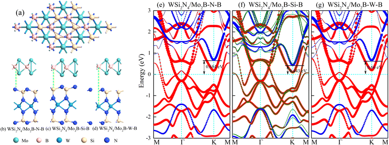
We examine the structural parameters of pristine WSi2N4 and Mo2B before investigating the WSi2N4/Mo2B heterostructures. The optimized lattice constants of WSi2N4 and Mo2B are 2.91 Å and 2.87 Å, respectively, which are in agreement with previous studies.45–47 A lattice mismatch of around 1.38% is obtained when WSi2N4 (1 × 1) and Mo2B (1 × 1) are vertically stacked. Three possible vertical stacking patterns are investigated, which are denoted as WSi2N4/Mo2B-N-B, WSi2N4/Mo2B-Si-B and WSi2N4/Mo2B-W-B [see Fig. 1(b)–(d)] in which the B atoms of Mo2B are directly aligned with the N, Si and W atoms of WSi2N4, respectively. To further characterize the interfacial stability and to determine the most energetically stable stacking configurations, the binding energy is calculated as Eb = (Eh − Em − Ew)/A, where the Eh, Ew and Em are the total energies of the heterostructures, isolated WSi2N4 and isolated Mo2B, respectively, and A is the surface area of the heterostructure supercell. The calculated binding energies are listed in Table 1. Here, the negative-valued Eb suggests that all three stacking configurations of WSi2N4/Mo2B are energetically stable and may be realized experimentally. Among the three stacking patterns, WSi2N4/Mo2B-Si-B stacking has the lowest Esb, thus suggesting its energetic stability. The interlayer spacing of the WSi2N4/Mo2B-Si-B stacking configuration is 2.32 Å, which is significantly lower than that of the other two stacking configurations.| WSi2N4/MoB2 | WSi2N4/MoB2O2 | WSi2N4/MoB2 (OH)2 | |||||||
|---|---|---|---|---|---|---|---|---|---|
| N–B | Si–B | W–B | N–O | Si–O | W–O | N–H | Si–H | W–H | |
| d (Å) | 3.344 | 2.32 | 3.538 | 3.023 | 2.491 | 2.615 | 1.785 | 2.081 | 1.969 |
| E b (eV Å−2) | −0.407 | −0.492 | −0.406 | −0.458 | −0.472 | −0.466 | −0.526 | −0.502 | −0.505 |
| Φ SB (eV) | 0.684, n | 0.443, n | 0.660, n | Ohmic contact, p | Ohmic contact, n | ||||
| Φ t (eV) | 3.079 | 0.168 | 3.291 | 6.013 | 5.486 | 5.676 | 0 | 0.812 | 0.43 |
| ω t (Å) | 1.156 | 0.08 | 1.4 | 1.63 | 1.13 | 1.27 | 0 | 0.54 | 0.37 |
| P t (%) | 12.5 | 96.7 | 7.4 | 1.66 | 6.64 | 4.5 | 100 | 24.1 | 77.9 |
| ρ t (10−9 Ω cm2) | 4.42 | 4.26 × 10⁻³ | 1.424 | 2.471 | 0.876 | 1.056 | 0 | 2.083 × 10⁻² | 1.527 × 10⁻² |
In Fig. 1(e)–(g), we show the projected band structure for the WSi2N4/Mo2B heterostructures. As the monolayers are coupled via weak van der Waals force, the absence of strong interlayer interactions enables the band structures of WSi2N4 and Mo2B to be well-preserved, with well-defined band edges of the semiconductor bands. The contact type and barrier height can usually be determined by the energy difference between the Fermi level and the semiconductor band edge in the heterostructure: Φn = ECBM − EF, Φp = EF − EVBM, where the ECBM and EVBM are the energy of the conduction band minimum and the valence band maximum of the semiconductor in the heterostructure, respectively. EF is the Fermi energy. Here, for all three stacking configurations of WSi2N4/Mo2B, the conduction bands are closer to the Fermi level, leading to an n-type Schottky contact with the Schottky barrier height (SBH) ranging from 0.443 eV to 0.684 eV (see Table 1). It is worth noting that the band structures of WSi2N4/Mo2B-N-B and WSi2N4/Mo2B-W-B are similar, giving rise to comparable SBH of 0.684 eV and 0.660 eV, respectively. However, the projected band structure of Mo2B in WSi2N4/Mo2B-Si-B near the Fermi level is obviously different from the other two stacking configurations, which arises from the closer interlayer distance and hence the slightly stronger interlayer interaction. Correspondingly, the SBH of the WSi2N4/MoB2-SiB stacking configuration is about 0.2 eV lower than that of the other two. In addition, using WSi2N4/Mo2B-Si-B as an example, we found that spin–orbit coupling (SOC) has little effect on the results [see Fig. 1(f)].
3.2. Interfacial properties of WSi2N4/Mo2B contact: interfacial charge transfer and tunneling barrier
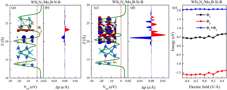
To confirm the stacking-dependent interlayer interaction observed above, we calculate the electrostatic potentials along the vertical direction of the heterostructures and the charge density differences according to Δρ = ρh − ρW − ρM, as displayed in Fig. 2(a)–(d). Here the ρh, ρW and ρM are the charge densities of the heterostructures, isolated WSi2N4 and Mo2B, respectively. The blue and red regions represent the charge depletion and accumulation. The stacking of different materials to form heterostructures breaks the original symmetry of the material, which causes charge redistribution across the interface. It can be clearly seen from Fig. 2(a)–(d) that there are significant differences in the amount of electron transfer between the two stacking configurations. There is only a small amount of charge transfer between WSi2N4 and Mo2B in WSi2N4/Mo2B-N-B, while a significantly larger amount of charge transfer occurs between WSi2N4 and Mo2B in the WSi2N4/Mo2B-Si-B configuration. The transfer of a sizable amount of electrons from WSi2N4 to Mo2B causes the Fermi level of Mo2B to energetically upshift, resulting in a smaller n-type SBH of the WSi2N4/Mo2B-Si-B configuration as compared to that of the WSi2N4/Mo2B-N-B configuration. The work function of isolated Mo2B is 4.897 eV, which changes to 4.624 eV in WSi2N4/Mo2B-Si-B, and 4.784 eV in WSi2N4/Mo2B-N-B, respectively, after forming a heterostructure with WSi2N4. It is worth noting that in addition to the Schottky barrier, the tunneling barrier at the interface of the semiconductor and metal also impedes the charge injection efficiency.48,49 The tunneling barrier height Φt and width wt of the heterostructures with different stacking configurations are summarized in Table 1, which are drastically different for the three configurations since the tunneling potential barrier is sensitively influenced by the spatial location and alignment of the atoms at the contacting interface. The tunneling barrier of WSi2N4/Mo2B-Si-B is extremely low, which means that the electron tunneling probability will be high. The tunneling probability (Pt) across the interface can be estimated as ,48–50 where the ωt is the full width at half-maximum of the potential barrier; ħ and m are the reduced Planck constant and the free electron mass, respectively; Φt represents the tunneling barrier height. The tunneling probability of WSi2N4/Mo2B-Si-B is calculated to be 96.7%, which is close to 100% as the Fermi level nearly crosses the tunneling potential barrier top. Such a high transparency suggests that the charge injection across the WSi2N4/Mo2B contact under the WSi2N4/Mo2B-Si-B stacking configuration is predominantly limited by the SBH instead of the interfacial tunneling barrier. The tunneling-specific resistivity (ρt) can also be estimated based on Simmons tunneling injection model:
  under intermediate bias voltages and
  when the ωt is too small.39,49 The calculated ρt is listed in Table 1.
We further find that the SBH under the WSi2N4/Mo2B-Si-B stacking configuration is robust against an external electric field, as shown in Fig. 2(e), which is in stark contrast to many heterostructures studied previously.35,36,51–54 An external electric field is thus ineffective in driving a Schottky-to-ohmic transition in the WSi2N4/Mo2B contact. Nevertheless, the robustness of the SBH of WSi2N4/Mo2B may be beneficial for achieving a stable Schottky diode operation. We further note that reducing the distance between the semiconducting and the metallic monolayers can also reduce the SBH. However, as the distance between Mo and N atoms is only 2.32 Å in WSi2N4/Mo2B-Si-B, which is close to the sum of their covalent radii, we do not expect further reducing the interlayer distance of WSi2N4/Mo2B to be a feasible way of contact-type tuning.
3.3. n-Type and p-type ohmic contact design via Mo2B surface engineering*
Modulating the metal work function provides an alternative way to tune the SBH. Since the outermost atoms of Mo2B are the Mo atom, there is an abundance of free electrons on its surface, which can stably adsorb other atoms or small molecules. Previous studies have demonstrated that Mo2B can be surface-engineered with O(Mo2BO2) or OH(Mo2B(OH)2) while still retaining its metallic nature, as well as its dynamic and thermal stability.47 Importantly, the work functions of the surface-engineered Mo2BO2 and Mo2B(OH)2 are significantly modulated to the high value of 7.39 eV and the low value of 3.14 eV, respectively, which is in stark contrast to the work function of 4.89 eV in the pristine Mo2B monolayer. Such significantly modulated work function immediately suggests surface engineering as a feasible approach to achieve n- and p-type ohmic contact to WSi2N4.To verify whether surface-engineered Mo2B can form ohmic contacts with WSi2N4, we reconstruct the WSi2N4 contact heterostructure using Mo2BO2 and Mo2B(OH)2 as the metal electrodes under the same set of stacking configurations (see Fig. 3 for the lattice structure and Table 1 for a summary of various contact parameters). Here we denote the stacking configurations as WSi2N4/Mo2BO2-(N, Si, W)-O and WSi2N4/Mo2B(OH)2-(N, Si, W)-H to denote the cases where (N, Si, W) is directly above the O or H atom. The Eb values of both WSi2N4/Mo2BO2 and WSi2N4/Mo2B(OH)2 contacts are negative, thus suggesting their energetic stability. The Eb of all stacking configurations of WSi2N4/Mo2B(OH)2 is generally lower than that of WSi2N4/Mo2B. The electronic structure characteristics of WSi2N4/Mo2BO2 and WSi2N4/Mo2B(OH)2 contacts are shown in Fig. 4. Intriguingly, the valence band of WSi2N4 in WSi2N4/Mo2BO2 and the conduction band of WSi2N4 in WSi2N4/Mo2B(OH)2 cross the Fermi level, which means that WSi2N4/Mo2BO2 and WSi2N4/Mo2B(OH)2 form p-type and n-type ohmic contacts, respectively, under all three different stacking configurations. The surface engineering of Mo2 with O or OH is thus an effective method to transform Mo2B into an ohmic electrode for WSi2N4.
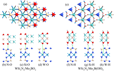 | ||
| Fig. 3 Top view and side view of the heterostructures of WSi2N4 contact with Mo2BO2 (a)–(d) and Mo2B(OH)2 (e)–(h), respectively. | ||
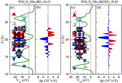
We now examine how the interfacial charge redistribution can shift the Fermi level upon forming a contact. To understand the role of Mo2BO2 and Mo2B(OH)2 in the charge transfer, using WSi2N4/Mo2BO2-Si-O and WSi2N4/Mo2B(OH)2-N-H as the respective examples, we calculate the plane-averaged electron density difference Δρ and the three dimensional isosurfaces, as depicted in Fig. 5. The electron accumulation region and depletion region are marked in red and blue, respectively. One can see that the charges are mainly accumulated in the Mo2BO2 layer, whereas they are depleted in the WSi2N4 layer for WSi2N4/Mo2BO2-Si-O (see Fig. 5(a) and (b)). However, the situation is reversed in WSi2N4/Mo2B(OH)2-N-H (see Fig. 5(c) and (d)). Thus, an opposite contact type is formed when WSi2N4 is in contact with Mo2BO2 and Mo2B(OH)2. Compared with WSi2N4/Mo2B-Si-B (see Fig. 2), we find that although the charge is depleted around the WSi2N4 layer, the electron activity area is mainly in the metal layer in WSi2N4/Mo2B-Si-B. However, the charge of the WSi2N4 layer is more affected. Surprisingly, the effective electrostatic potential of WSi2N4/Mo2B(OH)2-N-H exhibits zero interfacial tunneling barrier height, thus indicating that the WSi2N4/Mo2B(OH)2 ohmic contacts are compatible with high charge injection efficiency. This aspect is in contrast to WSi2N4/Mo2BO2 ohmic contact in which the interfacial tunneling barriers are significantly higher, with the best performing contact exhibiting a transmission probability of only Pt = 6.64% with the WSi2N4/Mo2BO2-Si-O stacking configuration, thus suggesting interfacial tunneling as a key factor that limits the charge injection across such a contact.
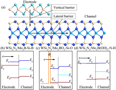
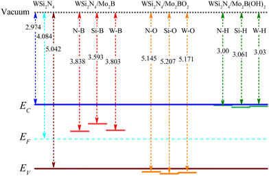
In addition to the Schottky barrier at the vertical contact interface between the semiconductor and the metal, the transport barrier between the lateral source/drain and the two-dimensional semiconductor channel interface is also another key factor that may influence the device performance. Fig. 6 shows a schematic drawing of the Mo2B-WSi2N4 interface outlining the charge transport pathway across the interface. The lateral SBH is calculated as: Φn,L = ECBM − EF and Φp,L = EF − EVBM, where the ECBM and EVBM are the energies of the CBM and VBM of pure WSi2N4. EF is the Fermi level of the heterostructure. The band edges of WSi2N4 and work functions of the heterostructures are summarized in Fig. 7. We present a schematic of the band alignments and electron injection mechanism in Fig. 6(b–d). For WSi2N4/Mo2B-Si-B, there are high barriers in both the vertical (0.443 eV) and lateral (0.619 eV) directions [see Fig. 6(b)]. The Fermi level of WSi2N4/Mo2BO2-Si-O is slightly lower than the VBM of pure WSi2N4, suggesting that lateral p-type ohmic contact can be formed in WSi2N4/Mo2BO2-Si-O, as shown in Fig. 6(c). Unfortunately, it has a very high tunneling barrier (5.486 eV). Similarly, the Fermi level of the WSi2N4/Mo2B(OH)2-N-H contact aligns nearly with the CBM energy of the WSi2N4 channel, giving rise to n-type quasi-ohmic contact with ultra-low SBH (0.026 eV), as is demonstrated in Fig. 6(d). The WSi2N4/Mo2B(OH)2 thus represents an exceptional ohmic contact with simultaneous n-type ohmic or quasi-ohmic behaviors along both vertical and lateral transport directions. The zero interfacial tunneling WSi2N4/Mo2B(OH)2 represents another practically useful feature that rarely occurs in other 2D/2D metal/semiconductor contacts.
4. Conclusion
In conclusion, we study the contact properties of WSi2N4 with Mo2B and Mo2B whose surface is fully saturated by O and OH groups using DFT calculations. WSi2N4 and Mo2B form n-type Schottky contacts in both the vertical and lateral directions, and the Schottky barrier in the vertical direction is robust to the electric field. p-Type ohmic contact is formed when WSi2N4 is in contact with Mo2BO2. Importantly, n-type ohmic contact with zero tunneling barrier in the vertical direction of the transistor and quasi-ohmic contact with ultra-low SBH in the lateral direction can be obtained in WSi2N4/Mo2B(OH)2, suggesting the potential role of WSi2N4/Mo2B(OH)2 in achieving an energy-efficient transistor device. Furthermore, the WSi2N4/Mo2BO2 contact, despite having a sizable interfacial tunneling barrier, similarly exhibits excellent p-type ohmic contact along the lateral direction. The simultaneous presence of n- and p-type contacts immediately suggests the potential of surface-engineered Mo2B metallic monolayers as an electrode materials to achieve WSi2N4-based CMOS device technology. Our results reveal surface engineering of 2D metallic monolayers as a feasible route towards energy-efficient 2D semiconductor electronic devices.Conflicts of interest
There are no conflicts to declare.Acknowledgements
The authors acknowledge support from the National Natural Science Foundation of China (Grant No. 12104136), Scientific Research Found of Hunan Provincial Education Department (Grant No. 21B0622 and 21C0549), Hunan Provincial Natural Science Foundation of China (No. 2022JJ40008 and No. 2023JJ30094), and Science Foundation of Hengyang Normal University of China (Grant No. 2021QD12). Y. S. A. is supported by the Singapore Ministry of Education (MOE) Academic Research Fund (AcRF) Tier 2 Grant (MOE-T2EP502210019) and the SUTD-ZJU IDEA Thematic Research Grant (SUTD-ZJU (TR) 202203).References
- R. K. Ratnesh, A. Goel, G. Kaushik, H. Garg, Chandan, M. Singh and B. Prasad, Mater. Sci. Semicond. Process., 2021, 134, 106002 CrossRef CAS.
- F. Schwierz, J. Pezoldt and R. Granzner, Nanoscale, 2015, 7, 8261 RSC.
- S. Das, A. Sebastian, E. Pop, C. J. McClellan, A. D. Franklin, T. Grasser, T. Knoblochm, Y. Illarionov, A. V. Penumatcha, J. Appenzeller, Z. Chen, W. Zhu, I. Asselberghs, L. Li, U. E. Avci, N. Bhat, T. D. Anthopoulos and R. Singh, Nat. Electron., 2021, 4, 786 CrossRef CAS.
- C. Liu, H. Chen, S. Wang, Q. Liu, Y. Jiang, D. W. Zhang, M. Liu and P. Zhou, Nat. Nanotechnol., 2020, 15, 545 CrossRef CAS PubMed.
- Q. H. Wang, K. Kalantar-Zadeh, A. Kis, J. N. Coleman and M. S. Strano, Nat. Nanotechnol., 2012, 7, 699 CrossRef CAS PubMed.
- S. Joseph, J. Mohan, S. Lakshmy, S. Thomas, B. Chakraborty, S. Thomas and N. Kalarikkal, Mater. Chem. Phys., 2023, 297, 127332 CrossRef CAS.
- M. Naguib, V. N. Mochalin, M. W. Barsoum and Y. Gogotsi, Adv. Mater., 2014, 26, 992 CrossRef CAS PubMed.
- A. Ahmed, S. Sharma, B. Adak, M. M. Hossain, A. M. LaChance, S. Mukhopadhyay and L. Sun, InfoMat, 2022, 4, e12295 CrossRef CAS.
- H. Liu, A. T. Neal, Z. Zhu, Z. Luo, X. Xu, D. Tomanek and P. D. Ye, ACS Nano, 2014, 8, 4033 CrossRef CAS PubMed.
- H. Liu, Y. Du, Y. Deng and P. D. Ye, Chem. Soc. Rev., 2015, 44, 2732 RSC.
- V. Cheudhary, P. Neugebauer, O. Mounkachi, S. Lahbabi and A. E. Fatimy, 2D Mater., 2022, 9, 032001 CrossRef.
- Y. Hong, Z. Liu, L. Wang, T. Zhou, W. Ma, C. Xu, S. Feng, L. Chen, M. Chen, D. Sun, X. Chen, H. Cheng and W. Ren, Science, 2020, 369, 670 CrossRef CAS PubMed.
- W. Fei, J. Trommer, M. C. Lemme, T. Mikolajick and A. Heinzig, InfoMat, 2022, 4, e12355 CrossRef CAS.
- S. B. Mitta, M. S. Choi, A. Nipane, F. Ali, C. Kim, J. T. Teherani, J. Hone and W. J. Yoo, 2D Mater., 2021, 8, 012002 CrossRef CAS.
- Y. S. Ang, L. Cao and L. K. Ang, InfoMat, 2021, 3, 502 CrossRef CAS.
- P. V. Pham, S. C. Bodepudi, K. Shehazad, Y. Liu, Y. Xu, B. Yu and X. Duan, Chem. Rev., 2022, 122, 6514 CrossRef CAS PubMed.
- D. S. Schulman, A. J. Amold and S. Das, Chem. Soc. Rev., 2018, 47, 3037 RSC.
- Y. Wang, S. Liu, Q. Li, R. Quhe, C. Yang, Y. Guo, X. Zhang, Y. Pan, J. Li, H. Zhang, L. Xu, B. Shi, H. Tang, Y. Li, J. Yang, Z. Zhang, L. Xiao, F. Pan and J. Lu, Rep. Prog. Phys., 2021, 84, 056501 CrossRef CAS PubMed.
- Y. Zheng, J. Gao, C. Han and W. Chen, Cell Rep. Phys. Sci., 2021, 2, 100298 CrossRef CAS.
- X. Liu, M. S. Choi, E. Hwang, W. J. Yoo and J. Sun, Adv. Mater., 2022, 34, 2108425 CrossRef CAS PubMed.
- L. Cao, G. Zhou, Q. Wu, S. Yang, H. Y. Yang, Y. S. Ang and L. K. Ang, Phys. Rev. Appl., 2020, 13, 054030 CrossRef CAS.
- C. S. Lau, J. Y. Chee, Y. S. Ang, S. W. Tong, L. Cao, Z. Ooi, T. Wang, L. K. Ang, Y. Wang, M. Chhowalla and K. E. J. Goh, ACS Nano, 2020, 14, 13700 CrossRef CAS PubMed.
- L. Cao, X. Deng, Z. Tang, G. Zhou and Y. S. Ang, Appl. Phys. Lett., 2022, 121, 113104 CrossRef CAS.
- P.-C. Shen, et al. , Nature, 2021, 593, 211 CrossRef CAS PubMed.
- T. Wu and J. Guo, Appl. Phys. Lett., 2022, 121, 023507 CrossRef CAS.
- W. Li, et al. , Nature, 2023, 613, 274 CrossRef CAS PubMed.
- T. Su, Y. Li, Q. Wang, W. Zhao, L. Cao and Y. S. Ang, J. Phys. D: Appl. Phys., 2023, 56, 234001 CrossRef.
- X. Ding, S. Zhang, M. Zhao, Y. Xiang, K. H. L. Zhang, X. T. Zu, S. Li and L. Qiao, Phys. Rev. Appl., 2019, 12, 064061 CrossRef CAS.
- B. Zhang, J. Zhou and Z. Sun, J. Mater. Chem. A, 2022, 10, 15965 Search PubMed.
- Y. Liu, P. Stradins and S. H. Wei, Sci. Adv., 2016, 2, e1600069 CrossRef PubMed.
- M. K. Mohanata and A. D. Sarkat, Appl. Surf. Sci., 2021, 540, 148389 CrossRef.
- Z. Xu, M. Chen and S. F. Liu, J. Phys. Chem. Lett., 2021, 12, 1718 CrossRef CAS PubMed.
- X. Zhang, L. Feng, S. Zhong, Y. Ye, H. Pan, P. Liu, X. Zheng, H. Li, M. Qu and X. Wang, Sci. China Mater., 2023, 66, 811 CrossRef CAS.
- Z. Li, Y. Zheng, G. Li, H. Wang, W. Zhu, H. Wang, Z. Chen, Y. Yuan, X. C. Zeng and Y. Wu, J. Phys. Chem. Lett., 2023, 14, 2941 Search PubMed.
- S. Nguyen, C. Q. Nguyen, Y. S. Ang, N. V. Hiang, N. M. Hung and C. V. Nguyen, Langmuir, 2023, 39, 6637 CrossRef CAS PubMed.
- C. V. Nguyen, Phys. Rev. B, 2021, 103, 115429 CrossRef CAS.
- C. C. Tho, C. Yu, Q. Tang, Q. Wang, T. Su, Z. Feng, Q. Wu, C. V. Nguyen, W. Ong, S. Liang, S. Guo, L. Cao, S. Zhang, S. A. Yang, L. K. Ang, G. Wang and Y. S. Ang, Adv. Mater. Interfaces, 2023, 10, 2201856 CrossRef CAS.
- Y. Yin, Q. Gong, M. Yi and W. Guo, Adv. Funct. Mater., 2023, 2214050 CrossRef CAS.
- C. C. Tho, S. Guo, S. Liang, W. L. Ong, C. S. Lau, L. Cao, G. Zhao and Y. S. Ang, Appl. Phys. Rev., 2023, 10, 041307 Search PubMed.
- L. Kong, Y. Chen and Y. Liu, Nano Res., 2021, 14, 1768 CrossRef CAS.
- G. Kresse and J. Furthmüller, Phys. Rev. B, 1996, 54, 11169 CrossRef CAS PubMed.
- G. Kresse and J. Furthmüller, Comput. Mater. Sci., 1996, 6, 15 CrossRef CAS.
- S. Grimme, J. Antony, S. Ehrlich and H. Krieg, J. Chem. Phys., 2010, 132, 154104 CrossRef PubMed.
- G. Kresse and D. Joubert, Phys. Rev. B, 1999, 59, 1758 CrossRef CAS.
- L. Wang, Y. Shi, M. Liu, A. Zhang, Y. Hong, R. Li, Q. Gao, M. Chen, W. Ren, H. Cheng, Y. Li and X. Chen, Nat. Commun., 2021, 12, 2361 CrossRef CAS PubMed.
- Z. Wang, S. W. Fan, H. G. Piao and Z. S. Lu, Appl. Surf. Sci., 2021, 538, 148026 CrossRef CAS.
- A. Shukla, G. Sharma and S. Krishnamurty, Appl. Surf. Sci., 2023, 615, 156299 CrossRef CAS.
- A. Allain, J. Kang, K. Banerjee and A. Kis, Nat. Mater., 2015, 14, 1195 CrossRef CAS PubMed.
- Q. Wang, L. Cao, S. Liang, W. Wu, G. Wang, C. H. Lee, W. L. Ong, H. Y. Yang, L. K. Ang, S. A. Yang and Y. S. Ang, npj 2D Mater. Appl., 2021, 5, 71 CrossRef CAS.
- Y. Wang, H. Yuan, Z. Li, J. Yang and A. C. S. Appl, Electron. Mater., 2022, 4, 1082 CAS.
- L. Cao, G. Zhou, Q. Wang, L. K. Ang and Y. S. Ang, Appl. Phys. Lett., 2021, 118, 013106 CrossRef CAS.
- J. E. Padilha, A. Fazzio and A. J. R. Silva, Phys. Rev. Lett., 2015, 114, 066803 CrossRef CAS PubMed.
- L. Cao, Y. S. Ang, Q. Wu and L. K. Ang, Appl. Phys. Lett., 2019, 115, 241601 CrossRef.
- N. T. T. Binh, C. Q. Nguyen, T. V. Vu and C. V. Nguyen, J. Phys. Chem. Lett., 2021, 12, 3934 CrossRef CAS PubMed.
| This journal is © The Royal Society of Chemistry 2024 |

