
 Open Access Article
 This Open Access Article is licensed under a
 Creative Commons Attribution 3.0 Unported Licence
Structural changes in HfSe2 and ZrSe2 thin films with various oxidation methods†
Alexandre C.
Foucher
 a,
Wouter
Mortelmans
a,
Wu
Bing
b,
Zdeněk
Sofer
b,
Rafael
Jaramillo
a and
Frances M.
Ross
*a
a,
Wouter
Mortelmans
a,
Wu
Bing
b,
Zdeněk
Sofer
b,
Rafael
Jaramillo
a and
Frances M.
Ross
*a
aDepartment of Materials Science and Engineering, Massachusetts Institute of Technology, Cambridge, Massachusetts 02139, USA. E-mail: fmross@mit.edu
bDepartment of Inorganic Chemistry, University of Chemistry and Technology Prague, Technická 5, 166 28 Prague 6, Czech Republic
First published on 10th June 2024
Abstract
HfSe2 and ZrSe2 transition metal dichalcogenide (TMD) films are of interest for their potential applications in field-effect transistors. To implement the use of these materials in devices, the formation of an oxide/TMD interface with well-defined dielectric/semiconductor properties is essential. The method by which the oxide is created, as well as any structural changes in the TMD under the conditions used for oxide formation, will affect the performance of both the dielectric and the semiconductor. In this work, we describe the structure of the oxide and the morphological changes occurring in HfSe2 and ZrSe2 under several oxidation conditions. Using in situ transmission electron microscopy, we show that room temperature oxidation in air causes segregation of Se and uneven surface oxidation. Exposure to O2 at high temperatures readily forms a crystalline oxide layer, although defects and cavities are also detectable. Finally, plasma oxidation forms a smoother and more uniform oxide layer than that formed by thermal oxidation. These results can guide the rational design of oxide/TMD interfaces for field-effect transistors and other electronic devices that incorporate HfSe2 and ZrSe2.
Introduction
HfSe2 and ZrSe2 are transition metal dichalcogenides (TMDs) that can be exfoliated into thin films with a nanoscale thickness. Although MoS2 and WS2 are the most widely used and studied TMDs,1–5 there has been an increasing interest in other compositions, especially Hf- and Zr-based materials. Recent studies have focused on implementing HfSe2 and ZrSe2 as two-dimensional semiconductors with native high-κ oxides HfO2 and ZrO2 respectively.6–9 This would be especially advantageous with a simple processing route in which direct oxidation of HfSe2 and ZrSe2 formed high-quality Hf or Zr oxides. Both HfSe2 and ZrSe2 are semiconductors with a band gap of approximately 1 eV in bulk, increasing to 1.2–1.5 eV for monolayer thickness;7,9,10 the HfO2 and ZrO2 band gaps are close to 5.5 eV and 5.3 eV, respectively, making these oxides good insulators.11,12 Hence, HfSe2 and ZrSe2 can form a semiconductor–insulator couple that is similar in bandgap to the widely-used Si–SiO2 combination, with band gaps 1.12 eV and approximately 9.3 eV respectively.13–15 An advantage of HfSe2 and ZrSe2 in comparison to Si is that they can readily be exfoliated to atomically thin 2D layers on which the an oxide layer can subsequently be formed.7 HfSe2/HfO2 and ZrSe2/ZrO2 stacks also offer benefits over MoS2 or WS2 as the semiconductor does not need to be combined with a dielectric of a different metal. Thus, HfSe2 and ZrSe2 can be considered for nanoscale, low-power devices, and recent reports have demonstrated that the oxide/TMD heterostructures (with oxidation in air) can be implemented in transistors to achieve promising electronic performance.7Creating the oxide/TMD interface requires either oxidation or deposition of oxide. One of the most widely used deposition methods for oxides is atomic layer deposition (ALD). This offers a high level of control over the oxide thickness, but delamination and poor contact at the oxide/TMDs interface have been observed.16 Indeed, with ALD, the top surface of the oxide is smooth but strain, roughness at the oxide/TMD interface, pinholes and delamination can impact the electronic performance of the materials.17,18 It is therefore useful to assess whether thermal oxidation to grow an oxide directly on the TMD may be a preferable alternative for the formation of heterostructures with a suitably smooth interface. Previous studies have focused on structural changes of HfSe2 flakes when oxidized but without direct comparison of oxidation structure and mechanisms of HfSe2 or ZrSe2 with different oxidation strategies.6
Thus, our aim is to understand the outcome of direct oxidation of TMDs (HfSe2 and ZrSe2) and determine potential degradation mechanisms in a reactive environment. In this work, we perform a detailed ex situ and in situ scanning transmission electron microscopy (STEM) analysis of HfSe2 and ZrSe2 films under various conditions to guide oxidation strategies for creating oxide/TMD heterostructures. We aim to understand structural changes that could be expected in the semiconductors and compare different oxidation processes to form an oxide/TMD interface. These experiments demonstrate that plasma oxidation tends to produce better-controlled oxide layers on these TMDs, whereas thermal oxidation (at low or high temperatures) causes the formation of substantial defects.
Experimental section
Materials
Hafnium (99.9%, −300 mesh) and zirconium powder (99.9%, −80 mesh) were obtained from Beijing Metallurgy and Materials Technology Co., Ltd. (China). Selenium (99.9999%, 1–6 mm granules) was bought from Wuhan Xinrong New Material Co. (China). Zirconium chloride (99.5%) and hafnium chloride (99.9%) were obtained from STREM (USA).Synthesis of bulk material and exfoliation
HfSe2 and ZrSe2 crystals were prepared by direct reaction from the elements in a quartz ampoule.19,20 All heating ramps used in the synthesis procedure were 0.5 °C min−1. Pre-reacted formed dichalcogenides in a quartz ampoule were placed in a horizontal two zone furnace and chemical vapor transport crystal growth was performed using a 100 °C thermal gradient. The source zone was kept at 1000 °C and the growth zone at 900 °C for 10 days. Formed crystals were removed from the ampoule inside an argon-filled glovebox.Sample preparation and electron microscopy
Ex situ and in situ STEM was performed using a Hitachi HF5000-IS instrument operating at 200 kV. Annular dark field, bright field and secondary electron images were collected simultaneously. For ex situ analysis (i.e. imaging and spectroscopy under standard vacuum conditions of 1 × 10⁻⁵ Pa and room temperature), cross-sectional samples were used. These samples were prepared using an FEI Helios Nanolab 600 Dual Beam System (FIB/SEM). For in situ analysis (i.e. investigation of the samples in a reactive atmosphere at elevated pressure and temperature), plan view samples were used. The bulk materials were first exfoliated with tape, which was then pressed onto a 90 nm thick SiO2 on Si wafer using 3 M Magic Scotch tape, leaving flakes on the surface. The flakes (5–20 layers thick) were then transferred onto TEM grids that included a SiNx window with holes and a microfabricated heating circuit (Norcada, Inc., Canada). These samples were imaged under vacuum or at pressures of 10 Pa H2 or O2. In situ energy dispersive spectroscopy (EDS) data were acquired with detectors provided by Oxford Instruments. All images and EDS were acquired after at least 30 minutes after exposure at the mentioned temperature and gas. Additional electron energy loss spectroscopy (EELS) data were collected with a JEOL NEOARM operating at 200 kV, using a K2 Summit Camera.Oxidation
The two procedures for forming the TMD/oxide heterostructures were thermal, achieved by heating exfoliated samples in O2in situ in the TEM, and oxygen plasma processing, to form an oxide layer on the top surface of few-layer TMD crystals that were subsequently made into cross-sectional samples for characterization. An oxygen plasma asher (AutoGlow) was used with an unheated sample (nominally at room temperature) of bulk HfSe2 and ZrSe2 crystals, placed in the chamber and pumped down to <0.5 Torr before introducing O2 gas and igniting the plasma.Spectroscopic ellipsometry (SE)
SE measurements were performed on the (001) basal planes (perpendicular to the optic axis) in the photon energy range 1.5 to 4.1 eV (800 to 300 nm). The ellipsometer (UV-NIR Vase, from J. A. Woollam) uses an automatic rotating analyzer and an auto-retarder. We perform all measurements on mirror-smooth surfaces and carry out all measurements at an angle of incidence of both 65° and 70°. Only the 70° angle data are presented. We then use SE analysis software to perform model-based analysis of the SE data. We use an optical model consisting of four layers: air, surface roughness, a thin oxide layer, and a semi-infinite bulk crystal. We assume that the dielectric properties of the oxide and underlying HfSe2 and ZrSe2 crystals remain unchanged. We model oxide surface roughness using the effective medium approximation, with the roughness being fixed by the results of atomic force microscopy (AFM) measurements on the same samples. We determine the complex refractive index (n, κ) for HfSe2 and ZrSe2 from SE measurements on freshly exposed surfaces, and we use a Cauchy model for the optical properties of the oxides.Results and discussion
The images shown in Fig. 1 summarize the main features observed in HfSe2 and ZrSe2 samples directly after fabrication by exfoliation. Additional images are shown in Fig. S1 (ESI†) to provide a comprehensive overview of the samples. HfSe2 and ZrSe2 belong to the trigonal crystal system with space group P![[3 with combining macron]](https://www.rsc.org/images/entities/char_0033_0304.gif) m1, with diffraction patterns provided in Fig. S2 (ESI†).21,22 In Fig. 1a, one can see that the edges of flakes are quickly oxidized to form amorphous HfO2 (or ZrO2), a result confirmed by electron energy loss spectroscopy in Fig. S3 (ESI†). The oxidation of the flakes occurred during exposure to air before the transfer of the samples into the TEM, which was a time period of below 10 minutes. Oxidation at the edges of 2D materials is a common phenomenon that has been reported previously.23,24 Overall, the results show that HfSe2 and ZrSe2 are sensitive to ambient conditions such that a brief exposure to air causes oxidation.
m1, with diffraction patterns provided in Fig. S2 (ESI†).21,22 In Fig. 1a, one can see that the edges of flakes are quickly oxidized to form amorphous HfO2 (or ZrO2), a result confirmed by electron energy loss spectroscopy in Fig. S3 (ESI†). The oxidation of the flakes occurred during exposure to air before the transfer of the samples into the TEM, which was a time period of below 10 minutes. Oxidation at the edges of 2D materials is a common phenomenon that has been reported previously.23,24 Overall, the results show that HfSe2 and ZrSe2 are sensitive to ambient conditions such that a brief exposure to air causes oxidation.
 | ||
| Fig. 1 HAADF-STEM images of HfSe2 and ZrSe2. (a) Plan-view image of exfoliated HfSe2 showing a crystalline structure consistent with Pm1. An amorphous layer of HfO2 has formed at the edges of the flakes. (b) Lower magnification image of exfoliated ZrSe2 showing a crystalline structure consistent with Pm1 and varying contrast. | ||
To further investigate changes due to oxidation, the samples were left exposed to air at room temperature for two weeks, and the results are summarized in Fig. 2. This exposure to air causes further amorphization (Fig. 2a) and the formation of particles on top of the films for both HfSe2 and ZrSe2, as seen in Fig. 2a and e. Energy-dispersive X-ray spectroscopy showing the spatial distribution of Hf, Zr, Se, and O reveals the segregation of Se. Segregation of Se was not observed in freshly exfoliated flakes (Fig. S4, ESI†). One can hypothesize that oxygen causes the displacement of Se atoms to form HfO2 and ZrO2. In fact, formation of HfO2-rich regions in HfSe2 upon oxidation in air at room temperature has been reported in a previous work.25 We also hypothesize that the oxidation of Hf and Zr causes migration and aggregation of Se to form the particles observed in Fig. 2g. Thus, the composition of the films is not uniform after prolonged oxidation under air and room temperature. We also observed similar results for flakes oxidized in air at 100 °C (Fig. S5, ESI†). We conclude that mild oxidation of HfSe2 and ZrSe2 under air, without annealing, does not spontaneously produce uniform oxide layers.
 | ||
| Fig. 2 EDS analysis of the two samples after exposure to air at room temperature for two weeks. (a)–(d) HfSe2 flake. (e)–(h) ZrSe2 flake. Oxidation and segregation of Se are shown by the EDS maps in (c) and (g). The particles in (e) are enriched in Se, based on the EDS analysis, as strong signal was collected only for Se (g). | ||
Since the oxidation of HfSe2 and ZrSe2 in mild conditions (air at room temperature) does not result in the morphology required for device applications, we investigated the effect of oxidation at high temperatures. Using in situ STEM, the temperature of the samples was ramped up at 1 °C min−1 in 10 Pa of O2. STEM images were collected as the temperature was progressively increased (200 °C, 400 °C, 600 °C, 800 °C). Further images and EDS data were collected after 1 hour of prolonged oxidation at 1000 °C. The results are shown in Fig. 2. By exploring this extreme temperature range, we could determine major structural changes that can be expected with HfSe2 and ZrSe2.
We first note that STEM images indicate that pits and cavities form in the films during thermal oxidation (Fig. 3). Fig. 3a and b shows the progressive changes in the flakes when the temperature is increased. Cavities become visible at temperatures above 800 °C for both samples, although in ZrSe2 changes in the morphology are visible even at 400 °C. Fig. 3c and d shows HAADF-STEM images with corresponding EDS maps after the sample was cooled down, showing the absence of Hf and O consistent with internal cavities and pits. Comparing STEM and SEM images (Fig. S6, ESI†) shows pits at the surface of heated HfSe2 and ZrSe2. A cross-section of the oxidized HfSe2 film shown in Fig. 3e confirms this conclusion. One can hypothesize that these changes during heating result from the accumulation of vacancies during Se removal and other internal movements of elements, ultimately causing the formation of pits and cavities. The formation and role of vacancies in TMDs have been reported and studied in previous publications.26,27 It has been shown that chalcogen vacancies are the most likely type of defects, due to a relatively low formation enthalpy. The formation of vacancies is often linked to reactions with oxygen and has been described in a previous study.26 The formation of cavities and pits suggests that oxidation at these highly elevated temperatures is not ideal for forming a uniform and defect-free oxide layer for implementation in nanodevices, even if the temperature were compatible with other processing steps. Oxidation causes voids and pits that would impact the electrical properties of the heterostructure and compromise the contact between the oxide and the TMD. Additional images of the progressive oxidation of HfSe2 and ZrSe2 in O2 (in situ STEM) show the formation of pits and cavities in the temperature range of 150–500 °C (Fig. S7, ESI†). Moreover, we oxidized HfSe2 and ZrSe2 in a furnace at 300 °C for 5 min (air at ambient pressure), as shown in Fig. S8 (ESI†). The results show cavities in the oxide layer and delamination at the oxide/TMD interface, underscoring that a thermal treatment to oxidize the samples is far from ideal.
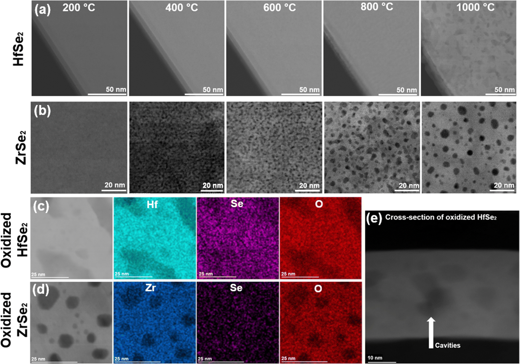 | ||
| Fig. 3 Investigation of HfSe2 and ZrSe2 crystals around 20 atomic layers in thickness after oxidation at high temperatures (after 30 min in O2 at 1000 °C). (a) and (b) HAADF-STEM image of HfSe2 and ZrSe2 at elevated temperatures in O2. Formation of cavities can be seen at high temperatures. (c) and (d) Oxidized samples with corresponding EDS maps. (e) FIB cut of oxidized HfSe2 confirming the presence of cavities. | ||
To see if the results of thermal oxidation can be modified, we explored the pre-treatment of HfSe2 and ZrSe2 by annealing in H2 or vacuum at elevated temperatures. Data for H2 is shown in Fig. 4 and data for vacuum annealing in Fig. S9 (ESI†). Our objective was to evaluate whether the amorphous oxides that could be detected in freshly exfoliated samples (Fig. 1) could be removed, and whether this might influence the formation of cavities on subsequent high temperature thermal oxidation. Indeed, as we have already discussed, oxidation at room temperature is not optimal as it is non-uniform and leads to segregation of Se. Thus, one could imagine annealing the sample first to remove heterogeneities and ultimately better control subsequent oxidation.
 | ||
| Fig. 4 In situ HAADF-STEM and SEM images of HfSe2 and ZrSe2 flakes after short exposure to air (before insertion in the TEM column) followed by reduction with H2 at 1000 °C for 30 min. (a)–(c) HfSe2 flakes with SEM images in (a) and (b) and bright-field-STEM images in (c). Epitaxial orientation between the islands and the underlying film can be seen. (d)–(f) HfSe2 flakes with SEM images in (d) and (e) and HAADF-STEM images in (f). Epitaxy between islands and thin film was also observed (shown by the white lines). Oxygen is detected everywhere, including in the small islands formed after reduction. | ||
The analysis was performed at temperatures increasing progressively to 1000 °C to determine major structural changes that can be expected with HfSe2 and ZrSe2. Changes at lower temperatures are minimal, and only above 800 °C is it possible to detect a strong morphological change, the formation of islands on the surface of the flakes (Fig. 4). Similar islands are also formed in vacuum (Fig. S10, ESI†). The in situ SEM images shown in Fig. 4 after prolonged exposure to H2 at 1000 °C indicate that these islands are aligned and have 3-fold or 6-fold symmetry, although some rectangular islands are visible. The alignment suggests epitaxial guiding by HfSe2 and ZrSe2. Indeed, epitaxy between nanoparticles and the TMD can be seen directly from the HAADF-STEM images in Fig. 4c and f. The atomic rows of the substrate are aligned with the crystal directions in the nano-islands. This was confirmed with a fast Fourier transform (FFT) analysis of areas over islands and the underlying HfSe2 or ZrSe2 flakes (Fig. S11, ESI†). EDS analysis of the islands in Fig. 4 shows some oxidation (Fig. S12, ESI†), so we conclude that these structures combine oxide and metals. The crystal structure of the oxides cannot be directly determined, but previous work suggest that monoclinic HfO2 and ZrO2 are stable in the considered temperature and pressure range.28,29 This indicates that oxygen in the initial flakes was not removed but remained in the crystal structure of the TMDs even under these highly reductive environments. Indeed, HfO2 and ZrO2 are thermodynamically highly stable, as reported previously.30,31
Annealing does not reduce the oxide but does appear able to change its structure. In the series of images during heating in H2 shown in Fig. S13 (ESI†), the initially amorphous oxides on the edges of the sample have re-crystallized. Based on measurements of the fast Fourier transform of the images, amorphous HfO2 and ZrO2 are reorganized into a crystal structure that is consistent with the P21/c structure reported in the literature.32,33 The change of structure is observed at 250–300 °C. This is consistent with previous reports34,35 in which transitions to a crystalline structure at elevated temperatures have been observed for amorphous HfO2 and ZrO2 on a crystalline substrate. EDS analysis indicates that the samples are still oxidized, even after annealing in H2. Overall, our experiments therefore show that oxidation at room temperature in air forms an amorphous oxide phase (ZrO2 or HfO2) while crystallization into a monoclinic crystal structure occurs after heating the sample above 250 °C.
After measurement of these changes under reducing conditions, the sample was cooled to room temperature, H2 was pumped out of the sample region and O2 was flowed, with results shown in Fig. 5. The sample was heated at the same ramp rate (1 °C s−1) as for the previous step. The features on the surface remained stable for a temperature up to 700 °C. At 950 °C, the features are almost non-distinguishable with SEM, and the surface roughness has substantially decreased. Thus, the islands formed on heating in vacuum or H2 are stable at elevated temperature (1000 °C) in these environments, but they disappear on exposure to oxygen. This might be advantageous in forming smooth surfaces: oxidation, in contrast to reduction, does not cause surface roughening, but yields a smoother oxide surface. It suggests that the surface smoothing is not due to surface diffusion at high temperatures but requires oxidation of the material. However, voids and cavities were still observed after the oxidation process, and the first annealing step in H2 or vacuum does not seem to impact the ultimate morphology after oxidation (Fig. 5k). Thus, one can conclude that a thermal pre-treatment (with H2) does not prevent the formation of cavities after oxidation at elevated temperatures. As an overall conclusion on the oxidation experiments, neither native oxidation in ambient conditions nor thermal oxidation at high temperatures form smooth, uniform, and defect-free oxide layers on these TMDs, and pre-treatment in H2 or vacuum at elevated temperatures to remove initial traces of oxides in the fresh flakes does not change the outcome.
 | ||
| Fig. 5 Oxidation of HfSe2 and ZrSe2 after pretreatment involving reduction with H2. (a)–(e) SEM images of ZrSe2 in which surface features are reduced at high temperatures. (f)–(j) Similar results obtained with SEM imaging of HfSe2. (k) HAADF-STEM image of oxidized HfSe2 after prolonged exposure to O2 at 1000 °C showing that oxidation still forms cavities. | ||
We finally perform plasma oxidation of HfSe2 and ZrSe2 flakes to determine if this oxidation method can produce more smooth and uniform oxide layers compared to thermal oxidation. The bulk samples were first exfoliated and (after 10 minutes of air exposure) plasma oxidation was performed for 2 minutes at 1000 W and 1 sccm of O2. AFM and ellipsometry data were collected before and after plasma oxidation to obtain the surface roughness and average thickness of the oxide layer, and cross-sectional TEM imaging was performed. The results are summarized in Fig. 6.
 | ||
| Fig. 6 Combined STEM imaging, ellipsometry and AFM study of bulk HfSe2 and ZrSe2 after plasma oxidation. (a) and (b) Images of the flakes with blue dots indicating the regions where AFM and ellipsometry were performed. (c) and (d) AFM image of the pristine and plasma-treated samples. The scale bar is 1 μm. (e) Ellipsometry data used for calculating the average surface roughness and oxide thickness. (f) and (g) Cross-sectional imaging of atypical regions showing delamination and a higher-than-average oxide layer. | ||
The AFM analysis of samples after oxidation shows an average surface roughness of 3.4 nm for both samples over the majority of the surface. AFM also shows the presence of protrusions at the μm-scale (Fig. 6c and d). (A lower density of similar protrusions is visible in as-exfoliated ZrSe2 samples.) We speculate that these micrometer-scale defects may originate from accumulation of Se and metals during the oxidation process. The roughness measured by AFM is slightly higher than that of other reference materials that we have oxidized under similar plasma oxidation conditions, such as MoS2 (3.0 nm) or HfS2 (2.0 nm).
In terms of the oxide thickness, ellipsometry produces a value (Fig. 6e) of 3.5 ± 0.4 nm on HfSe2 and 3.2 ± 0.2 nm on ZrSe2. This is lower than the measured oxide layer thickness of 5–8 nm seen in the STEM images in Fig. 6f and g. These differences may arise from the challenge of modelling the optical properties of the oxide layer throughout its depth.
In terms of the structure and composition, STEM imaging of HfSe2 and ZrSe2 in Fig. 6f and g shows that plasma oxidation creates a smooth and amorphous oxide layer (HfO2 or ZrO2) on top of a crystalline TMD (additional images are provided in Fig. S14, ESI†). The amorphous oxide can be crystallized after annealing.35 No cavities were observed, and EDS analysis shows a uniform composition (Fig. S14 and S15, ESI†). We expect from the annealing experiments that this oxide can be transformed into a crystalline structure after its formation, as is commonly done with ALD-deposited oxides. The absence of internal cavities or pits with the plasma oxidation process is a clear benefit compared to thermal oxidation methods. However, some delamination (as seen from EDS data of ZrSe2 in Fig. S15, ESI†) can be observed and the micrometer-scale defects seen with AFM are an obstacle for implementing the oxide/TMD heterostructure into devices. The analysis of plasma oxidation of HfSe2 and ZrSe2 also underlines a difference compared to HfS2 plasma oxidation, which has been reported to be very successful.36,37 Even though plasma oxidation is not without issues, it still appears to be the best method to avoid compositional heterogeneities and nanoscale defects such as pits and cavities. Particles seen in Fig. 6c and d are an issue and undesirable, but plasma oxidation still represents an improvement compared to thermal oxidation as the nanoscale structure of the oxide layer is of better quality.
Conclusion
Through analysis with multiple techniques, we find a variety of structural changes in HfSe2 and ZrSe2 as a result of different oxidation methods. Ex situ microscopy shows a tendency of Se to segregate upon oxidation at room temperature, creating compositional heterogeneities. In situ STEM analysis revealed the results of oxidation at high temperatures, with the formation of an oxide layer without compositional heterogeneities, but with cavities. We also showed that a pre-treatment in vacuum or H2 at high temperature followed by oxidation does not prevent the formation of cavities. Plasma oxidation appears to be a more favorable method to form an oxide layer without cavities or compositional heterogeneities, even though some delamination and defects were observed. This work underlines the structural modifications in HfSe2 and ZrSe2 in reductive and oxidative environments and thereby may help to establish guidelines for implementing these materials and their native oxides in novel transistors and other electronic devices.Conflicts of interest
The authors declare no competing interests.Acknowledgements
This work was funded in part by Semiconductor Research Corporation (SRC) under contract no. 2021-NM-3027. This work was supported by the Office of Naval Research (ONR) MURI through grant no. N00014-17-1-2661. This work was performed with the use of facilities and instrumentation supported by NSF through the Massachusetts Institute of Technology Materials Research Science and Engineering Center DMR-1419807. This work was performed in part through the use of MIT.nano's facilities. Z. S. was supported by ERC-CZ program (project LL2101) from the Ministry of Education Youth and Sports (MEYS), Czech Republic.References
- K. Reidy, W. Mortelmans, S. Soon Jo, A. Penn, B. Wang, A. Foucher, F. M. Ross and R. Jaramillo, Nano Lett., 2023, 23, 5894–5901 CrossRef CAS PubMed.
- A. Nourbakhsh, A. Zubair, R. N. Sajjad, T. K. G. Amir, W. Chen, S. Fang, X. Ling, J. Kong, M. S. Dresselhaus, E. Kaxiras, K. K. Berggren, D. Antoniadis and T. Palacios, Nano Lett., 2016, 16, 7798–7806 CrossRef CAS PubMed.
- H. Kim, W. Kim, M. O’Brien, N. McEvoy, C. Yim, M. Marcia, F. Hauke, A. Hirsch, G. T. Kim and G. S. Duesberg, Nanoscale, 2018, 10, 17557–17566 RSC.
- A. Sebastian, R. Pendurthi, T. H. Choudhury, J. M. Redwing and S. Das, Nat. Commun., 2021, 12, 1–12 CrossRef PubMed.
- M. W. Iqbal, M. Z. Iqbal, M. F. Khan, M. A. Shehzad, Y. Seo, J. H. Park, C. Hwang and J. Eom, Sci. Rep., 2015, 5, 1–9 Search PubMed.
- Q. Yao, L. Zhang, P. Bampoulis and H. J. W. Zandvliet, J. Phys. Chem. C, 2018, 122, 25498–25505 CrossRef CAS PubMed.
- M. J. Mleczko, C. Zhang, H. R. Lee, H. H. Kuo, B. Magyari-Kope, Z. X. Shen, R. G. Moore, I. R. Fisher, Y. Nishi and E. Pop, Device Res. Conf. - Conf. Dig. DRC.
- J.-M. Zhang, X.-Y. Gao, X.-M. Wei, Y.-H. Huang, A. Ali and I. Shahid, Thin Solid Films, 2022, 755, 139332 CrossRef CAS.
- X. Zhao, H. Zhang, T. Chen, Y. Gao, H. Wang, T. Wang and S. Wei, Superlattices Microstruct., 2018, 120, 659–669 CrossRef CAS.
- K. E. Aretouli, P. Tsipas, D. Tsoutsou, J. Marquez-Velasco, E. Xenogiannopoulou, S. A. Giamini, E. Vassalou, N. Kelaidis and A. Dimoulas, Appl. Phys. Lett., 2015, 106, 143105 CrossRef.
- E.-S. R. Khattab, S. S. Abd, E. Rehim, W. M. I. Hassan and T. S. El-Shazly, ACS Omega, 2021, 6, 30061–30068 CrossRef CAS PubMed.
- M. K. Hudait and Y. Zhu, Cit. J. Appl. Phys., 2013, 113, 17–314 Search PubMed.
- H. E. Romero, N. Shen, P. Joshi, H. R. Gutierrez, S. A. Tadigadapa, J. O. Sofo and P. C. Eklund, ACS Nano, 2008, 2, 2037–2044 CrossRef CAS PubMed.
- B. J. Hinds, K. Nishiguchi, A. Dutta, T. Yamanaka, S. Hatanani and S. Oda, Jpn. J. Appl. Phys., 2000, 39, 4637–4641 CrossRef CAS.
- R. E. Hummel, Electronics Properties of Materials, Springer, 2011, 4th edn Search PubMed.
- M. H. Heyne, D. Chiappe, J. Meersschaut, T. Nuytten, T. Conard, H. Bender, C. Huyghebaert, I. P. Radu, M. Caymax, J. F. De Marneffe, E. C. Neyts and S. De Gendt, J. Mater. Chem. C, 2016, 4, 1295–1304 RSC.
- M. Luisier, A. Szabo, C. Stieger, C. Klinkert, S. Bruck, A. Jain and L. Novotny, Tech. Dig. - Int. Electron Devices Meet. IEDM, 2017, 5.4.1–5.4.4 Search PubMed.
- F. Sadeghi-Tohidi, D. Samet, S. Graham and O. N. Pierron, Sci. Technol. Adv. Mater., 2014, 15, 8 CrossRef PubMed.
- P. K. Roy, N. Antonatos, T. Li, Y. Jing, J. Luxa, J. Azadmanjiri, P. Marvan, T. Heine and Z. Sofer, ACS Appl. Mater. Interfaces, 2023, 15, 1859–1870 CrossRef CAS PubMed.
- K. Lee, B. M. Szydłowska, O. Hartwig, K. Synnatschke, B. Tywoniuk, T. Hartman, T. Tomašević-Ilić, C. P. Gabbett, J. N. Coleman, Z. Sofer, M. Spasenović, C. Backes and G. S. Duesberg, J. Mater. Chem. C, 2023, 11, 593–599 RSC.
- The Materials Project, Materials Data on HfSe2 by Materials Project, 2020.
- The Materials Project, Materials Data on ZrSe2 by Materials Project, 2020.
- J. Martincová, M. Otyepka and P. Lazar, 2D Mater., 2020, 7, 045005 CrossRef.
- T. T. Pham, R. Castelino, A. Felten and R. Sporken, Surf. Interfaces, 2022, 28, 101681 CrossRef CAS.
- Q. Yao, L. Zhang, P. Bampoulis and H. J. W. Zandvliet, J. Phys. Chem. C, 2018, 122, 25498–25505 CrossRef CAS PubMed.
- A. Dabral, A. K. A. Lu, D. Chiappe, M. Houssa and G. Pourtois, Phys. Chem. Chem. Phys., 2019, 21, 1089–1099 RSC.
- R. L. H. Freire, F. C. De Lima and A. Fazzio, Phys. Rev. Mater., 2022, 6, 084002 CrossRef CAS.
- A. S. Bazhenov and K. Honkala, Top. Catal., 2017, 60, 382–391 CrossRef CAS.
- G. R. Waetzig, S. W. Depner, H. Asayesh-Ardakani, N. D. Cultrara, R. Shahbazian-Yassar and S. Banerjee, Chem. Sci., 2016, 7, 4930–4939 RSC.
- S. Stemmer, J. Vac. Sci. Technol., 2024, B 22, 791–800 Search PubMed.
- A. Ruiz Puigdollers, F. Illas and G. Pacchioni, ACS Omega, 2017, 2, 3878–3885 CrossRef CAS PubMed.
- V. Rani, A. Sharma, A. Kumar, P. Singh, S. Thakur, A. Singh, Q. Van Le, V. H. Nguyen and P. Raizada, Catal., 2022, 12, 1418 CAS.
- A. J. Lee, B. S. Kim, J. H. Hwang, Y. Kim, H. Oh, Y. J. Park and W. Jeon, Appl. Surf. Sci., 2022, 590, 153082 CrossRef CAS.
- S. Kim, Y. Oshima, N. Nakajima, N. Hashikawa, K. Asayama and K. Takayanagi, Thin Solid Films, 2012, 520, 2562–2565 CrossRef CAS.
- X. Y. Zhang, J. Han, D. C. Peng, Y. J. Ruan, W. Y. Wu, D. S. Wuu, C. J. Huang, S. Y. Lien and W. Z. Zhu, Nanomaterials, 2022, 12, 3890 CrossRef CAS PubMed.
- T. Jin, Y. Zheng, J. Gao, Y. Wang, E. Li, H. Chen, X. Pan, M. Lin and W. Chen, ACS Appl. Mater. Interfaces, 2021, 13, 10639–10649 CrossRef CAS PubMed.
- X. Wang, S. K. Ghosh, M. Afshar-Mohajer, H. Zhou, Y. Liu, X. Han, J. Cai, M. Zou and X. Meng, J. Mater. Res., 2020, 35, 804–812 CrossRef CAS.
Footnote |
| † Electronic supplementary information (ESI) available: Additional STEM images, EELS spectra, EDS maps. See DOI: https://doi.org/10.1039/d3tc04698b |
| This journal is © The Royal Society of Chemistry 2024 |