Strain-induced tunable valley polarization and topological phase transition in SVSiN2 monolayer†
Yunxi
Qi
 a,
Can
Yao
a,
Jun
Zhao
a,
Can
Yao
a,
Jun
Zhao
 *a and
Hui
Zeng
 *b
*b
aNew Energy Technology Engineering Laboratory of Jiangsu Province & School of Science, Nanjing University of Posts and Telecommunications, Nanjing, Jiangsu 210023, China. E-mail: zhaojun@njupt.edu.cn
bSchool of Microelectronics, Nanjing University of Science and Technology, Nanjing, Jiangsu 210094, China. E-mail: zenghui@njust.edu.cn
First published on 20th February 2024
Abstract
The potential application of a two-dimensional (2D) ferrovalley semiconductor in the field of valleytronics has sparked extensive research interest. Using first-principles calculations, we predict that the SVSiN2 monolayer is a promising ferrovalley material with excellent dynamical and thermal stability, and its Curie temperature is around room temperature. A giant valley polarization of −72.73 meV is obtained by shifting the magnetization direction from in-plane to out-of-plane. The valley-contrasting properties of the SVSiN2 monolayer can be remarkably modulated by in-plane strains. Most importantly, topological phase transition is predicted to be realized by a 5.5–6% tensile strain, which is verified by the nonzero Chern number and the nontrivial edge state. Compared to the in-plane strain modulation, the valley-dependent properties of the SVSiN2 monolayer are robust to vertical electric fields. Our findings could enrich the physical understanding of the effects of manipulating the valley-dependent properties of 2D ferrovalley semiconductors, facilitating potential applications of 2D Janus monolayers for valleytronics.
1 Introduction
A valley, which is defined as a local extremum in momentum space, can be used to manipulate information encoding, transfer, and processing.1 Correspondingly, valleytronics that relying on manipulating the emergent degree of freedom of a valley, has received increasing research focus in recent years.2 However, valleys may degenerate in terms of energy aspect due to the protection of time reversal symmetry. As a result, breaking the degeneracy of valleys is crucial for fabricating high-storage density and low-energy electronic devices.3 Over the past decade, the 2D transition metal dichalcogenides (TMDs) monolayer with broken inversion symmetry and spin–orbit coupling (SOC) has extensively promoted the development of valleytronics.4–7 Non-equilibrium distributions for valley carriers in TMDs can be realized by many routes, including the valley contrasting optical selection rule, the Zeeman effect of the external magnetic field, magnetic atom doping, and magnetic proximity effect.6–11 However, some drawbacks are accompanied with the implementation of these routes. For example, the optical pumping method demands harsh experimental conditions. The efficiency of valley polarization generated by an external magnetic field is very low. Regarding magnetic atom doping, it may lead to unstable valley polarization as a result of introducing impurity scattering between different valleys. Fortunately, the 2D intrinsic ferrovalley materials provide new opportunities to solve these issues. Therefore, it is necessary to explore novel intrinsic ferrovalley semiconductors (FVS) with emerging valley-related properties.Monolayered FVS exhibit not only spontaneous valley polarization, but also valley-contrasting transport under the optical selection rule resulting from spin-valley coupling. This is attributed to the presence of inherent long-range ferromagnetism combined with the SOC effect, and furthermore, the ferromagnetism is crucial because it breaks the time-reversal symmetry of the system.12,13 In addition, some emergent quantum states, such as topological states and half-valley-metal (HVM) states, are predicted to be achievable using a finite strain on the FVS material.14,15 However, only a few 2D materials are shown to exhibit spontaneous valley polarization, such as the monolayers of 2H-VSe2,16 Nb3I8,17 NbX2,18 and GdI2.19 Moreover, most 2D monolayers under consideration essentially possess an in-plane easy magnetization axis. In contrast, the FVS materials with tunable multiple valley states and out-of-plane magnetization are rarely reported.20 Correspondingly, searching for a new intrinsic FVS materials is of great importance to broaden the practical application of the valleytronics.21
To date, most intrinsic FVS materials are synthesized or proposed on the basis of binary or ternary chemical compounds.22–27 In recent years, layered 2D materials MoSi2N4 and WSi2N4 have been prepared through chemical vapor deposition (CVD).28 Many theoretical investigations are devoted to the understanding of MA2Z4 (M = Cr, Mo, W, V, Nb, Ta, Ti, Zr or Hf; A = Si or Ge; and Z = N, P, As) based 2D materials, using first principles calculations. The MA2Z4 family has emerging topological, magnetic, valley, superconducting, and catalytic properties.29–34 Hence, the physical properties of various MA2Z4-based van der Waals (vdW) heterostructures have also been investigated to explore their electronic and optoelectronic applications.35,36
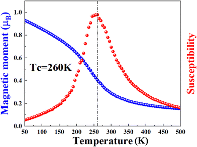
In this work, we propose a Janus SVSiN2 monolayer with five layers of atoms, which can be obtained from the VSi2N4 monolayer by replacing one side of the N–Si–N atom with an S atom. It can be regarded as a 2D Janus material with reflection symmetry breaking.37 The SVSiN2 monolayer is predicted to be a FVS material with a Curie temperature of 260 K. It has excellent thermal and dynamical stability. We predict that a large valley polarization of −72.73 meV can be achieved by switching the magnetization direction of the SVSiN2 monolayer from the in-plane direction to the out-of-plane direction. A tight-binding model is used to elucidate the anomalous valley Hall effect (AVHE) induced by the valley polarization and the opposite Berry curvatures at the K/−K valleys in the SVSiN2 monolayer. Strain and electric field are also introduced to tune the valley polarization and Berry curvature of the system. Most importantly, a biaxial tensile strain of 5.5–6% can induce valley quantum anomalous Hall effect. Our findings broaden the knowledge of 2D ferrovalley materials and deepen the understanding of strain-induced topological and valley states in the Janus SVSiN2 monolayer.38–41
2 Computational methods
All our first-principles calculations are based on density functional theory (DFT) implemented using the Vienna ab initio simulation package (VASP).42,43 The Perdew–Burke–Ernzerhof (PBE) exchange–correlation function of the generalized gradient approximation (GGA) was utilized to calculate the structural relaxation and electronic structure.44 We use the GGA+U method to describe the strong correlation correction of V-3d orbitals. We test various U-values and compare them with the electronic structures obtained from the hybrid functional HSE06,45 which typically gives an accurate electronic structure. It is found that the calculated results obtained from GGA+U and HSE06 agree well when Ueff = 3.2 eV. To avoid interlayer interactions, a vacuum layer of 20 Å is considered along the z-axis direction. The cutoff energy is 500 eV for the plane-wave basis. To fully optimize the structure, the convergence criteria for total energy and atomic residual force are 1 × 10⁻⁸ eV and 0.001 eV Å−1, respectively. The first Brillouin zone integration is carried out using 16 × 16 × 1 Γ-centered k-grids.46 The 9 × 16 × 1 Monkhorst–Pack k-meshes are used to calculate ferromagnetic (FM)/antiferromagnetic (AFM) energy using rectangular superlattices. Table S1 (ESI†) shows that the effects of dipole correction on the geometric structure and electronic property are negligible. The calculations regarding the SVSiN2 monolayer will not consider the dipole correction hereafter. The SOC effect is considered to study the magnetocrystalline anisotropy and electronic properties of the SVSiN2 monolayer. The phonon dispersion of a 4 × 4 × 1 supercell is calculated using density functional perturbation theory and PHONOPY code.47 The ab initio molecular dynamics (AIMD) simulations were carried out using a 4 × 4 × 1 supercell at 300 K. The VASPBERRY subroutine is used to calculate the materials' Berry curvature and circular polarization.48 In addition, we construct the maximum localized Wannier function (MLWF) using the WANNIER90 package,49 and calculate the edge states and anomalous Hall conductivity with the help of WANNIERTOOLS subroutine.50 Based on the Heisenberg model, we perform Monte Carlo (MC) simulations on a 10 × 10 × 1 supercell using the multi-dimensional Curie Temperature Simulation Package.51 All crystal structures are visualized by VESTA software.523 Results and discussion
3.1 Atomic structure and stability
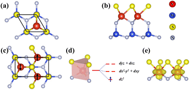
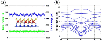
We first study the atomic and electronic structures of SVSiN2, as shown in Fig. 1(a) and (b). The stacking order of the SVSiN2 monolayer is S–V–N–Si–N, which can be considered to be a Janus structure. The lattice constant of the SVSiN2 monolayer is a = b = 2.952 Å. The crystal symmetry of the SVSiN2 monolayer is C3v. Similar to the TMDs, the inversion symmetry of the SVSiN2 monolayer is also broken. We conduct AIMD simulations to explore the thermal stability of the SVSiN2 monolayer, as illustrated in Fig. 2(a).During a simulation time of 5 ps, the simulated results show that the total energy fluctuation is not significant, and is always near the equilibrium value at a temperature of 300 K. As shown in the inset of Fig. 2(a), there is no significant structural break in the final snapshot of the SVSiN2 monolayer. The calculated AIMD result indicates that the SVSiN2 monolayer possesses excellent thermal stability at room temperature. The phonon dispersion shown in Fig. 2(b) illustrates that there is no imaginary frequency in any branches, ensuring the dynamical stability of the SVSiN2 monolayer. The structural stability is evaluated by its formation energy (Eform), which is defined as:
 | (1) |
3.2 Magnetic ground state
We investigate the electron occupancy in V atoms based on crystal field theory. In a trigonal prismatic crystal field environment, the V-d orbitals split into a low-lying dz2 orbital, followed by (dxy, dx2−y2) and (dxz, dyz) orbitals. Among them, an unpaired electron occupies the dz2 orbital, which is evidenced by the spin density distribution of the occupied V-d orbital exhibited in Fig. 1(d) and (e), which generates a net magnetic moment of 1μB into the SVSiN2 monolayer. In Fig. S1(a) (ESI†), we evaluate the effects of different Ueff values on the magnetic moments of the V atom. The calculated results show that the atomic magnetic moments obtained are in the range 2–4 eV, which agrees well with the theoretical values. The average distance between two V atoms in the SVSiN2 is 2.952 Å. Such a large atomic distance results in a weak direct exchange interaction force between the V atoms. And the super-exchange mechanism is considered to dominate the interaction between V atoms since the V–N–V angle is close to 90°. According to the Goodenough–Kanamori rule,54,55 the SVSiN2 monolayer adopts FM-ordered ground states and forms FM coupling, which is attributed to the overlap of V-dz2 and N-p orbitals.We also calculate the energy difference (ΔE) with respect to different Ueff values between the AFM- and FM-ordered states by ΔE = EAFM − EFM, as presented in Fig. S1(b) (ESI†). The rectangular supercell shown in Fig. 1(c) is employed for the ΔE calculation. The results indicate that the SVSiN2 monolayer remains in the FM ground state with the Ueff value changing within the range 0–5 eV. Compared to the calculated ΔE results under different Ueff with the corresponding HSE06 results, we find that two calculations agree well when Ueff = 3.2 eV. The calculated local magnetic moment of the system in Fig. S1(a) (ESI†) is about 1.044μB with Ueff = 3.2 eV, which is consistent with the above analysis in Fig. 1(d). Moreover, the band structures of the SVSiN2 monolayer under different Ueff values is shown in Fig. S2 (ESI†). It can be seen that the SVSiN2 is a half-metal when Ueff = 0 eV. When the Ueff value changes in the range 3–4 eV, the band structure of the SVSiN2 monolayer is qualitatively consistent with that obtained from HSE06. In addition, the projected density of states shown in Fig. S3 (ESI†) demonstrates that there is no significant difference in orbital contributions between PBE+U and HSE06. Therefore, in the following discussion, we choose Ueff = 3.2 eV to investigate the spin valley coupling of the SVSiN2 monolayer.
When the SOC effect is considered, the direction of susceptibility depends on the area where the electron clouds overlap, which can be described by the magnetic anisotropy energy (EMAE) and is calculated by:
| EMAE = EMCA + EMSA | (2) |
| EMCA = E[100] − E[001] | (3) |
 | (4) |
 represents the magnetic moment of the V atom at position i, and
  represents the vector of V atoms at positions i and j. Correspondingly, EMSA can be expressed as:
 | (5) |
 and
and  . The EMCA values calculated at different k-meshes are plotted in Fig. S4 (ESI†). It is noted that the EMCA results are almost unchanged when the k-meshes are increased from 16 × 16 × 1 to 28 × 28 × 1, indicating that a converged result is obtained. The EMAE is predicted to be −93.08 μeV with EMCA = −75.88 μeV and EMSA = −17.20 μeV. Our calculated value of EMSA agrees well with EMSA = −17 μeV reported in the case of the monolayered VSiGeN4.58 It is noticed that the calculated EMSA values are approximately −14 to −17 μeV for VSiGeN4 (−16 μeV) and VSiSnN4 (−14 μeV) and VSi2N4 (−17 μeV) monolayers,59 suggesting that the D–D interaction between the V atoms are very similar. In contrast, the EMCA is defined as the energy difference between the in-plane (x-direction) spin configuration and out-of-plane (z-direction) spin configuration. Our calculated EMSA indicates that the SOC effect makes the SVSiN2 monolayer have in-plane spin configuration, which is more prominent than that in the VSi2N4 monolayer (EMCA = −42 to −64 μeV).29,59 Moreover, we calculated the influence of different Ueff values on EMCA. With the enhancement of the Coulomb repulsion effect, it is expected to induce the spin configuration of the SVSiN2 monolayer to shift from an in-plane to out-of-plane direction. This anticipation is confirmed by Fig. S5 (ESI†). The calculated EMCA is found to change to a positive value when Ueff = 5 eV. Hence, the negative EMAE means that the magnetization axis of the SVSiN2 monolayer is parallel to the plane of the monolayer, revealing that the SVSiN2 monolayer is a 2D XY magnet.60,61 In principle, the magnetization orientation of the SVSiN2 monolayer can be elaborately modulated from the in-plane direction to the out-of-plane direction by overcoming a 93.08 μeV energy barrier. Furthermore, the negative EMAE is also obtained in the 2D VSi2N4 and Janus VSiGeN4 and VSiSnN4 monolayers.59
To further explore the nature of the in-plane EMAE, we calculate the orbital contribution of the V atom to the EMCA, as shown in Fig. S6 (ESI†). For V-d orbitals, the in-plane EMCA is mainly contributed by hybridization of dxy/dx2−y2, dz2/dyz, and dz2/dxz. However, the EMCA contribution of the V atom in the V-p orbital is one order of magnitude greater than that in the V-d orbital. Therefore, the in-plane EMAE mainly originates from the hybridization of the p-orbitals. The Curie temperature (Tc) of the SVSiN2 monolayer is estimated on the basis of the Heisenberg model:
 | (6) |
3.3 Electronic structure
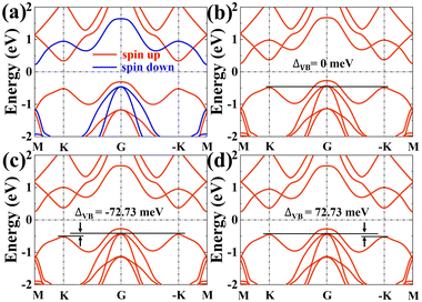
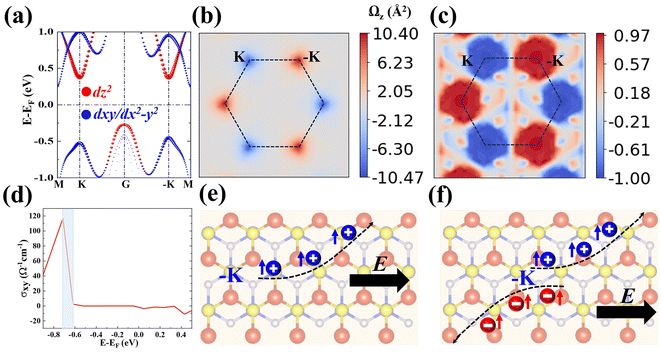
The band structure of the SVSiN2 monolayer is shown in Fig. 4. When the SOC is not considered, the electronic bands are completely spin polarized, as shown in Fig. 4(a). The valence band maximum (VBM) and conduction band minimum (CBM) of the SVSiN2 monolayer is located at the G and M point, respectively, leading to an indirect bandgap of about 0.53 eV. We define the valley splitting of the valence band ΔVB (conduction band ΔCB) as:| ΔVB = EVBK − EVB−K(ΔCB = ECBK − ECB−K) | (7) |
To further examine the characteristics of valley splitting in the SVSiN2 monolayer, we derive a simple model to describe the intensity of valley splitting for the SVSiN2 monolayer:67
 | (8) |
 | (9) |
![[L with combining circumflex]](https://www.rsc.org/images/entities/i_char_004c_0302.gif) ·Ŝ are based on d-orbitals.68 The valence band (conduction band) valley splitting can be expressed as:
·Ŝ are based on d-orbitals.68 The valence band (conduction band) valley splitting can be expressed as:| ΔCB = 〈dz2|Ĥsoc|dz2〉 − 〈dz2|Ĥsoc|dz2〉 = 0 | (10) |
 | (11) |
When the magnetization direction is parallel to the x-axis, Ĥsoc = λ![[L with combining circumflex]](https://www.rsc.org/images/entities/i_char_004c_0302.gif) x, the valley of the valence band (conduction band) splits into ΔCB = ΔVB = 〈ψv1|λ
x, the valley of the valence band (conduction band) splits into ΔCB = ΔVB = 〈ψv1|λ![[L with combining circumflex]](https://www.rsc.org/images/entities/i_char_004c_0302.gif) x|ψv1〉 − 〈ψv−1|λ
x|ψv1〉 − 〈ψv−1|λ![[L with combining circumflex]](https://www.rsc.org/images/entities/i_char_004c_0302.gif) x|ψv−1〉 = 0. The above analyses are consistent with our valley splitting results obtained from first principles calculations. The significant differences between valence band valley splitting and conduction band valley splitting are attributed to different basis functions determined by different orbital contributions of different K/−K valleys.
x|ψv−1〉 = 0. The above analyses are consistent with our valley splitting results obtained from first principles calculations. The significant differences between valence band valley splitting and conduction band valley splitting are attributed to different basis functions determined by different orbital contributions of different K/−K valleys.
For 2D hexagonal lattices, there may be anomalous Hall effects in the FVS materials without the assistance of a magnetic field. In the following, we will study the valley-related transport properties of the SVSiN2 monolayer. The transport properties related to valleys are closely related to the Berry curvature. For a 2D system, the Berry curvature can be expressed as:
 | (12) |
 the non-zero and opposite Berry curvatures indicate that the SVSiN2 monolayer exhibit opposite anomalous velocities at the K/−K valleys. In contrast, the Berry curvature is close to zero at other positions in the momentum space. The anomalous Hall conductivity σxy can be calculated by integrating the Berry curvature over the whole occupied states:71
 . As shown in Fig. 5(d), the presence of AVHE is confirmed by the non-zero σxy highlighted by the shaded area. Furthermore, we have proposed a theoretical design to achieve AVHE, as shown in Fig. 5(e). Owing to the remarkable valley splitting of VBM at the K/−K valleys, we can modulate the EF to achieve hole doping at the desired valley, e.g., the −K valley shown in Fig. 4(c).
In addition, the non-zero berry curvature indicates that the K/−K valley has chirality, in which the circularly polarized light selection rule can be described as:
 | (13) |
Using a specific frequency of right circularly polarized light, an electron–hole pair with the same spin can be generated at the −K valley, and the electron (hole) will accumulate at the top (bottom) of the sample, as shown in Fig. 5(f). The valley-contrasting transport properties are similar to those in the MoS2 monolayer.66
3.4 Strain effects and topological phase transition
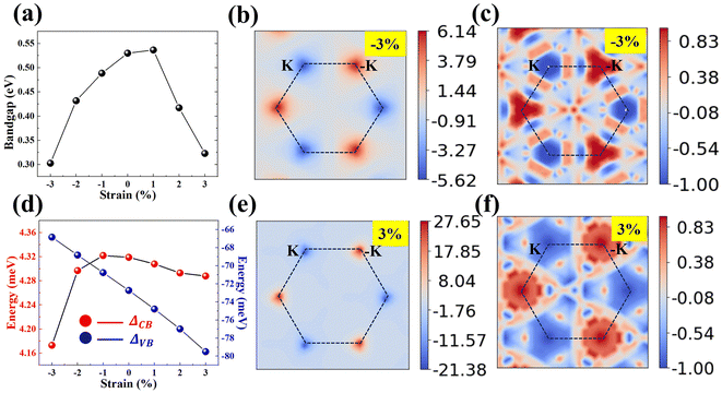
The exchange interaction in the SVSiN2 monolayer is related to the overlap of orbital wave functions between ions. Therefore, the distance between magnetic ions or the distance (bond angle) between magnetic ions and ligand atoms, has a substantial impact on the electronic properties of the SVSiN2 monolayer. Strain engineering has been widely used to modulate the electronic structure of 2D materials. One of the main advantages of 2D materials is that their tensile properties are much higher than their bulk counterparts.73 Therefore, we examine the effect of biaxial strain within ±3% on the electronic structure of the SVSiN2 monolayer. Here, the biaxial strain is simulated by changing the lattice constant of the crystal cell and can be defined as: | (14) |
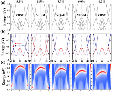
The in-plane biaxial strains give rise to the prominent influence on the Berry curvature at the K/−K valleys, as shown in Fig. 6(b) and (e). The variation of the Berry curvature at the K/−K valleys is consistent with the trend of valley splitting of the valence band, i.e., a tensile strain induces a greater Berry curvature difference at the K/−K valleys. Furthermore, both the CBM and VBM at the K/−K valleys are shifted towards the EF when a tensile strain is applied, as shown in Fig. S9 (ESI†). It is expected that the bandgap at the K/−K valleys could be closed when a sufficiently large strain is performed on the SVSiN2 monolayer. Most importantly, the bandgap closure generally implies the presence of a strain-driven topological transition associated with a nontrivial electronic state.74 We therefore calculate the orbital-resolved electronic structure and edge states of the SVSiN2 monolayer under 5.3–6.2% biaxial strain.
It can be seen from Fig. 7(a) and (b) that the SVSiN2 monolayer is a valley-half-semiconductor (VHSC) when ε < 5.5%. In contrast, the bandgap of the SVSiN2 monolayer at the −K valley is essentially closed when a strain of ε = 5.5% is applied. Moreover, the VBM at the −K valley is contributed by the dz2 orbital of the V atom, revealing the presence of strain-driven band inversion. Therefore, a valley-half-semimetal (VHSM) state is obtained under ε = 5.5%. When the tensile strain is continuously increased, the bandgap at the −K valley reopens and the SVSiN2 monolayer enters the valley quantum anonymous Hall (VQAH) state. When ε = 6%, the bandgap of the SVSiN2 monolayer at the K valley is closed, and a similar band inversion for the CBM is clearly observed at the K valley. Similar strain induced valley-dependent band inversion was also observed in the VSi2N4 monolayer and Janus VSiGeN4 monolayer.34,41,58 The band inversion is a strong implication of the nontrivial topological phase.40,74 The bandgap at the K valley reopens and the SVSiN2 monolayer becomes VHSC when ε > 6%.
To understand the mechanism of multiple topological phase transitions, we analyzed the orbital projection band structure and edge states, as shown in Fig. 7(c). Under a tensile strain of 5.7%, it is found that an edge state crosses the Fermi level, and it connects the VBM at the K valley and the CBM at the −K valley. The strain induced edge state in the SVSiN2 monolayer is very similar to the case of the strained (4.5–4.8%) VSiCN4 monolayer.41 The topologically nontrivial phase is characterized by the nonzero topology invariant. The Chern number ![[Doublestruck C]](https://www.rsc.org/images/entities/char_e166.gif) is obtained by integrating the Berry curvature in the first Brillouin zone, and the calculated
is obtained by integrating the Berry curvature in the first Brillouin zone, and the calculated ![[Doublestruck C]](https://www.rsc.org/images/entities/char_e166.gif) in the strain range 5.5–6% is −1. The nonzero topology invariant shows that the 5.5–6.0% strained SVSiN2 monolayer possesses nonzero intrinsic quantum anomalous Hall conductivity σxy according to:74
in the strain range 5.5–6% is −1. The nonzero topology invariant shows that the 5.5–6.0% strained SVSiN2 monolayer possesses nonzero intrinsic quantum anomalous Hall conductivity σxy according to:74
σxy = −![[Doublestruck C]](https://www.rsc.org/images/entities/char_e166.gif) G0 G0 | (15) |
 is the quantum conductance. The VQAH is predicated to be achieved in the SVSiN2 monolayer using a 6% in-plane tensile strain. The SVSiN2 monolayer provides a new platform to explore valley-contrasting properties and strain-driven topological state transitions.
3.5 Effects of external electric field
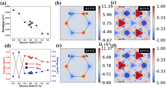
In addition, we explore the effects of external electric field on the valleytronics properties of the SVSiN2 monolayer, as shown in Fig. 8. The bandgap of the SVSiN2 monolayer exhibits a decreasing trend in the range from negative electric field to positive electric field. Compared to the strain modulation, the vertical electric field gives rise to negligible influence on the bandgap variation, as confirmed in Fig. 8(a). Fig. S10 (ESI†) demonstrates that their band structures are almost unaffected by the electric field. The valleytronic properties of the SVSiN2 monolayer are robust to the vertical electric fields. Therefore, the vertical electric field has a weak impact on the valley splitting and Berry curvature, as verified in Fig. 8(b)–(f). The different tuning behavior of biaxial strains and vertical electric fields on the SVSiN2 monolayer enrich the understanding of its valley-dependent properties, and are helpful to the development of FVS devices.4 Conclusions
Based on first-principles calculations, we have demonstrated that the SVSiN2 monolayer is a promising FVS material. Our calculation results indicate that: (1) the SVSiN2 monolayer is a 2D XY magnetic material with a Curie temperature of 260 K, and its in-plane magnetic anisotropy energy mainly originates from the hybridization of the p-orbitals, exhibiting excellent thermal and dynamical stability. (2) A giant valley polarization of −72.73 meV and opposite Berry curvatures can be achieved in the SVSiN2 monolayer by shifting the magnetization from the in-plane to out-of-plane direction, leading to an anomalous valley Hall effect. (3) The valley-contrasting properties of the SVSiN2 monolayer can be significantly tuned by in-plane biaxial strains. Specifically, the 5.5–6.0% strain driven topological phase transition is confirmed by the band inversion and nontrivial edge state. The calculated nonzero Chern number demonstrates that the strained SVSiN2 monolayer possesses nonzero intrinsic quantum anomalous Hall conductivity to realize the valley polarized quantum anomalous Hall effect. (4) Compared to the in-plane strain modulation, the valley-related property of the SVSiN2 monolayer is rather robust to the vertical electric fields. Overall, our research has broadened the scope of 2D FVS materials, which is beneficial for practical applications of the SVSiN2 monolayer for valleytronic devices.Conflicts of interest
The authors declare that they have no known competing financial interests or personal relationships that could have appeared to influence the work reported in this paper.Acknowledgements
This work was supported by the National Natural Science Foundation of China (No. 62174088 and 62371238). We are grateful to the High-Performance Computing Centre of Nanjing University for providing the IBM Blade cluster system.References
- D. Xiao, W. Yao and Q. Niu, Phys. Rev. Lett., 2007, 99, 236809 CrossRef.
- J. R. Schaibley, H. Yu, G. Clark, P. Rivera, J. S. Ross, K. L. Seyler, W. Yao and X. Xu, Nat. Rev. Mater., 2016, 1, 16055 CrossRef CAS.
- A. Rycerz, J. Tworzydlo and C. W. J. Beenakker, Nat. Phys., 2007, 3, 172–175 Search PubMed.
- H. Zeng, J. Dai, W. Yao, D. Xiao and X. Cui, Nat. Nanotechnol., 2012, 7, 490–493 CrossRef CAS.
- G. Aivazian, Z. Gong, A. M. Jones, R.-L. Chu, J. Yan, D. G. Mandrus, C. Zhang, D. Cobden, W. Yao and X. Xu, Nat. Phys., 2015, 11, 148–152 Search PubMed.
- K. F. Mak, K. He, J. Shan and T. F. Heinz, Nat. Nanotechnol., 2012, 7, 494–498 CrossRef CAS PubMed.
- A. Srivastava, M. Sidler, A. V. Allain, D. S. Lembke, A. Kis and A. Imamoglu, Nat. Phys., 2015, 11, 141–147 Search PubMed.
- D. MacNeill, C. Heikes, K. F. Mak, Z. Anderson, A. Kormányos, V. Zólyomi, J. Park and D. C. Ralph, Phys. Rev. Lett., 2015, 114, 037401 CrossRef CAS PubMed.
- P. Back, M. Sidler, O. Cotlet, A. Srivastava, N. Takemura, M. Kroner and A. Imamoğlu, Phys. Rev. Lett., 2017, 118, 237404 CrossRef PubMed.
- R. Peng, Y. Ma, S. Zhang, B. Huang and Y. Dai, J. Phys. Chem. Lett., 2018, 9, 3612–3617 CrossRef CAS PubMed.
- J. Zhao, X. Jin, H. Zeng, C. Yao and G. Yan, Appl. Phys. Lett., 2021, 119, 213101 CrossRef CAS.
- W.-Y. Tong, S.-J. Gong, X. Wan and C.-G. Duan, Nat. Commun., 2016, 7, 13612 CrossRef CAS PubMed.
- Z. He, R. Peng, X. Feng, X. Xu, Y. Dai, B. Huang and Y. Ma, Phys. Rev. B, 2021, 104, 075105 CrossRef CAS.
- H. Huan, Y. Xue, B. Zhao, G. Gao, H. Bao and Z. Yang, Phys. Rev. B, 2021, 104, 165427 CrossRef CAS.
- H. Hu, W. Y. Tong, Y. H. Shen, X. Wan and C. G. Duan, npj Quantum Mater., 2020, 6, 7 CrossRef.
- J. Liu, W.-J. Hou, C. Cheng, H.-X. Fu, J.-T. Sun and S. Meng, J. Phys.: Condens. Matter, 2017, 29, 255501 CrossRef PubMed.
- R. Peng, Y. Ma, X. Xu, Z. He, B. Huang and Y. Dai, Phys. Rev. B, 2020, 102, 035412 CrossRef CAS.
- Y. Zang, Y. Ma, R. Peng, H. Wang, B. Huang and Y. Dai, Nano Res., 2021, 14, 834–839 CrossRef CAS.
- H.-X. Cheng, J. Zhou, W. Ji, Y.-N. Zhang and Y.-P. Feng, Phys. Rev. B, 2021, 103, 125121 CrossRef CAS.
- S.-D. Guo, Y.-L. Tao, H.-T. Guo, Z.-Y. Zhao, B. Wang, G. Wang and X. Wang, Phys. Rev. B, 2023, 107, 054414 CrossRef CAS.
- J.-D. Zheng, Y.-F. Zhao, Y.-F. Tan, Z. Guan, N. Zhong, F.-Y. Yue, P.-H. Xiang and C.-G. Duan, J. Appl. Phys., 2022, 132, 120902 CrossRef CAS.
- K. Sheng, B. Zhang, H.-K. Yuan and Z.-Y. Wang, Phys. Rev. B, 2022, 105, 195312 CrossRef CAS.
- S.-D. Guo, Y.-L. Tao, G. Wang, S. Chen, D. Huang and Y. S. Ang, Front. Phys., 2024, 19, 23302 CrossRef.
- W. Pan, Phys. Rev. B, 2022, 106, 125122 CrossRef CAS.
- W. Zhou, G. Zheng, Z. Wan, T. Sun, A. Li and F. Ouyang, Appl. Phys. Lett., 2023, 123, 143101 CrossRef CAS.
- R. Li, N. Mao, X. Wu, B. Huang, Y. Dai and C. Niu, Nano Lett., 2023, 23, 91–97 CrossRef CAS.
- L. Cai, R. Li, X. Wu, B. Huang, Y. Dai and C. Niu, Phys. Rev. B, 2023, 107, 245116 CrossRef CAS.
- Y.-L. Hong, Z. Liu, L. Wang, T. Zhou, W. Ma, C. Xu, S. Feng, L. Chen, M.-L. Chen, D.-M. Sun, X.-Q. Chen, H.-M. Cheng and W. Ren, Science, 2020, 369, 670–674 CrossRef CAS.
- Q. Cui, Y. Zhu, J. Liang, P. Cui and H. Yang, Phys. Rev. B, 2021, 103, 085421 CrossRef CAS.
- X. Feng, X. Xu, Z. He, R. Peng, Y. Dai, B. Huang and Y. Ma, Phys. Rev. B, 2021, 104, 075421 CrossRef CAS.
- L. Yan, B.-T. Wang, X. Huang, Q. Li, K. Xue, J. Zhang, W. Ren and L. Zhou, Nanoscale, 2021, 13, 18947–18954 RSC.
- Y. Liu, Y. Ji and Y. Li, J. Phys. Chem. Lett., 2021, 12, 9149–9154 CrossRef CAS PubMed.
- Y. Feng, Z. Wang, X. Zuo and G. Gao, Appl. Phys. Lett., 2022, 120, 092405 CrossRef CAS.
- X. Zhou, R.-W. Zhang, Z. Zhang, W. Feng, Y. Mokrousov and Y. Yao, npj Comput. Mater., 2021, 7, 160 CrossRef.
- Y. Qi, C. Yao, J. Zhao and H. Zeng, Phys. Chem. Chem. Phys., 2023, 25, 28104–28112 RSC.
- J. Wang, Z. Zhang, J. Shen, M. Zhang, L. Niu and L. Bai, J. Phys. Chem. C, 2023, 127, 18067–18075 CrossRef CAS.
- J. Zhao, Y. Qi, C. Yao and H. Zeng, Phys. Rev. B, 2024, 109, 035408 CrossRef CAS.
- Y. Yin, Q. Gong, M. Yi and W. Guo, Adv. Funct. Mater., 2023, 33, 2214050 CrossRef CAS.
- C. C. Tho, S.-D. Guo, S.-J. Liang, W. L. Ong, C. S. Lau, L. Cao, G. Wang and Y. S. Ang, Appl. Phys. Rev., 2023, 10, 041307 CAS.
- X.-S. Guo and S.-D. Guo, Phys. Chem. Chem. Phys., 2023, 25, 18577–18583 RSC.
- P. Li, X. Yang, Q.-S. Jiang, Y.-Z. Wu and W. Xun, Phys. Rev. Mater., 2023, 7, 064002 CrossRef CAS.
- G. Kresse and J. Furthmüller, Phys. Rev. B: Condens. Matter, 1996, 54, 11169–11186 CrossRef CAS PubMed.
- G. Kresse and J. Hafner, Phys. Rev. B: Condens. Matter, 1993, 47, 558–561 CrossRef CAS PubMed.
- J. P. Perdew, K. Burke and M. Ernzerhof, Phys. Rev. Lett., 1996, 77, 3865–3868 CrossRef CAS PubMed.
- J. Heyd, G. E. Scuseria and M. Ernzerhof, J. Chem. Phys., 2003, 118, 8207–8215 CrossRef CAS.
- H. J. Monkhorst and J. D. Pack, Phys. Rev. B: Solid State, 1976, 13, 5188–5192 CrossRef.
- A. Togo and I. Tanaka, Scr. Mater., 2015, 108, 1–5 CrossRef CAS.
- S.-W. Kim, H.-J. Kim, S. Cheon and T.-H. Kim, Phys. Rev. Lett., 2022, 128, 046401 CrossRef CAS PubMed.
- N. Marzari, A. A. Mostofi, J. R. Yates, I. Souza and D. Vanderbilt, Rev. Mod. Phys., 2012, 84, 1419–1475 CrossRef CAS.
- Q. Wu, S. Zhang, H.-F. Song, M. Troyer and A. A. Soluyanov, Comput. Phys. Commun., 2018, 224, 405–416 CrossRef CAS.
- Y. Zhang, B. Wang, Y. Guo, Q. Li and J. Wang, Comput. Mater. Sci., 2021, 197, 110638 CrossRef CAS.
- K. Momma and F. Izumi, J. Appl. Crystallogr., 2011, 44, 1272–1276 CrossRef CAS.
- R. T. Sibatov, R. M. Meftakhutdinov and A. I. Kochaev, Appl. Surf. Sci., 2022, 585, 152465 CrossRef CAS.
- J. B. Goodenough, Phys. Rev., 1955, 100, 564–573 CrossRef CAS.
- J. Kanamori, J. Phys. Chem. Solids, 1959, 10, 87–98 CrossRef CAS.
- D.-S. Wang, R. Wu and A. J. Freeman, Phys. Rev. B: Condens. Matter, 1993, 47, 14932–14947 CrossRef CAS PubMed.
- C. Pellegrini, T. Müller, J. K. Dewhurst, S. Sharma, A. Sanna and E. K. U. Gross, Phys. Rev. B, 2020, 101, 144401 CrossRef CAS.
- S.-D. Guo, W.-Q. Mu, J.-H. Wang, Y.-X. Yang, B. Wang and Y.-S. Ang, Phys. Rev. B, 2022, 106, 064416 CrossRef CAS.
- D. Dey, A. Ray and L. Yu, Phys. Rev. Mater., 2022, 6, L061002 CrossRef CAS.
- K. Sheng, Q. Chen, H.-K. Yuan and Z.-Y. Wang, Phys. Rev. B, 2022, 105, 075304 CrossRef CAS.
- J. L. Lado and J. Fernandez-Rossier, 2D Mater., 2017, 4, 035002 CrossRef.
- W.-B. Zhang, Q. Qu, P. Zhu and C.-H. Lam, J. Mater. Chem. C, 2015, 3, 12457–12468 RSC.
- H. Sun, S.-S. Li, W.-X. Ji and C.-W. Zhang, Phys. Rev. B, 2022, 105, 195112 CrossRef CAS.
- Y. Qi, C. Yao, J. Zhao and H. Zeng, Phys. Rev. B, 2023, 108, 125304 CrossRef CAS.
- Q. Li, C.-X. Zhang, D. Wang, K.-Q. Chen and L.-M. Tang, Mater. Adv., 2022, 3, 2927–2933 RSC.
- D. Xiao, G.-B. Liu, W. Feng, X. Xu and W. Yao, Phys. Rev. Lett., 2012, 108, 196802 CrossRef PubMed.
- D. Dai, H. Xiang and M.-H. Whangbo, J. Comput. Chem., 2008, 29, 2187–2209 CrossRef CAS PubMed.
- S. Konschuh, M. Gmitra and J. Fabian, Phys. Rev. B: Condens. Matter Mater. Phys., 2010, 82, 245412 CrossRef.
- C. Ke, Y. Wu, W. Yang, Z. Wu, C. Zhang, X. Li and J. Kang, Phys. Rev. B, 2019, 100, 195435 CrossRef CAS.
- Y. Yao, L. Kleinman, A. H. MacDonald, J. Sinova, T. Jungwirth, D.-S. Wang, E. Wang and Q. Niu, Phys. Rev. Lett., 2004, 92, 037204 CrossRef PubMed.
- D. J. Thouless, M. Kohmoto, M. P. Nightingale and M. den Nijs, Phys. Rev. Lett., 1982, 49, 405–408 CrossRef CAS.
- T. Cao, G. Wang, W. Han, H. Ye, C. Zhu, J. Shi, Q. Niu, P. Tan, E. Wang, B. Liu and J. Feng, Nat. Commun., 2012, 3, 887 CrossRef PubMed.
- L. Zhang, Y. Tang, A. R. Khan, M. M. Hasan, P. Wang, H. Yan, T. Yildirim, J. F. Torres, G. P. Neupane, Y. Zhang, Q. Li and Y. Lu, Adv. Sci., 2020, 7, 2002697 CrossRef CAS.
- X.-L. Qi and S.-C. Zhang, Rev. Mod. Phys., 2011, 83, 1057–1110 CrossRef CAS.
Footnote |
| † Electronic supplementary information (ESI) available. See DOI: https://doi.org/10.1039/d3tc04759h |
| This journal is © The Royal Society of Chemistry 2024 |

