 Open Access Article
A NaBiF4:Gd/Tb nanoscintillator for high-resolution X-ray imaging†
Manisha
Bungla
ab,
Mohit
Tyagi
c,
Ashok K.
Ganguli
 *bd and
Paras N.
Prasad
 *a
*a
aDepartment of Chemistry and The Institute for Lasers, Photonics and Biophotonics, University at Buffalo (SUNY), 14260 Buffalo, NY, USA. E-mail: pnprasad@buffalo.edu
bDepartment of Chemistry, Indian Institute of Technology Delhi, Hauz Khas, New Delhi 110016, India. E-mail: ashok@chemistry.iitd.ac.in
cTechnical Physics Division, Bhabha Atomic Research Centre, Trombay, Mumbai 400085, India
dDepartment of Chemical Sciences, Indian Institute of Science Education & Research, Laudigam, Berhampur, Odisha 760003, India
First published on 8th May 2024
Abstract
Lanthanide doped fluoride nanoscintillators have received tremendous attention due to their high photochemical stability and tunable X-ray excited optical luminescence compared to traditional inorganic scintillators. Advancement in this field requires design strategies for the development of nanoscintillators that offer tailorable excitation dynamics through nanostructuring, thus enabling high luminescence in a suitable host. However, selection of an appropriate host matrix with low phonon energy and a nanoarchitecture that mitigates surface quenching due to the large surface-to-volume ratio of nanoparticles is still a challenge. Herein, we introduce NaBiF4:Gd,Tb (NBF) nanoparticles as highly efficient nanoscintillators with reduced afterglow to minimize interference in radioimaging, which utilizes the high X-ray attenuation coefficient of bismuth (5.74 cm2 g−1 at about 100 keV). The host NaBiF4 has a high refractive index and low phonon energy, which reduces the multiphonon non-radiative relaxation rates and enhances the radiative emission probability, thus yielding a long-life time for luminescence. Furthermore, by varying the composition of the nanoparticles and the relative concentrations of Gd and Tb, luminescence at multiple wavelengths in changing relative intensities can be achieved to enable multiplexed imaging. We show that NaBiF4:Gd/Tb can be easily synthesized using the co-precipitation method at room temperature within 1 min. Furthermore, we succeeded in fabricating organic–inorganic nanocomposite self-standing films of NaBiF4:Gd,Tb in high loading, uniformly dispersed in poly(methyl methacrylate) (PMMA) polymer. Their application in radiography is demonstrated by recording X-ray images using a commercially available charge-coupled device camera. We attained a resolution comparable to the non-flexible commercial CsI (TI) scintillator and significantly superior to the commercial Gd2O2S:Tb, GOS:Tb scintillators commonly used for screens.
1. Introduction
Scintillators act as an energy transformer, converting high-energy X-rays into low energy visible or ultraviolet photons.1–3 These are broadly employed to actualize X-ray excited optical luminescence (XEOL) imaging in security inspections and industrial materials4–6 as well as in medical imaging7–9 and space explorations.10,11 Conventional scintillators (for example: NaI:Tl,12 Lu3Al5O12:Ce13 and Bi4Ge3O1214) have been successfully developed and applied to a variety of commercial X-ray detectors. However, these traditional inorganic scintillators are typically confined to bulk crystals, and exhibit uncontrollable particle sizes,15,16 non-uniform morphology,17 non-tunable XEOL wavelength,18,19 and limited conversion efficiency, hindering their practical utility.20,21 As a result, it would be critical to investigate innovative methods for developing highly efficient and cost-effective scintillators22,23 to overcome the aforementioned constraints and fulfil the rising needs of X-ray imaging technologies.Lanthanide-doped fluoride nanoscintillators have received tremendous attention due to their high photochemical stability24–28 and tunable X-ray excited optical luminescence29,30 compared to the traditional inorganic scintillators. However, the limited availability and high cost of rare earth compounds restricts the commercialization of these scintillator materials.31–33 As a consequence, development of less expensive and non-rare earth and environmentally friendly host materials for scintillators is required urgently. Fortunately, elements like bismuth can substitute the rare earth element in NaREF4-based matrices with comparable performance.34,35 The advancements in this field demand the development of nanoscintillators with tailorable excitation dynamics through effective nanostructuring, facilitating high luminescence within a suitable host matrix. However, a significant research gap persists in the selection of an appropriate host matrix with low phonon energy and a nanoarchitecture that mitigates surface quenching, a consequence of the large surface-to-volume ratio in nanoparticles.
Herein, we introduce NaBiF4:Gd,Tb (NBF) nanoparticles as a highly efficient nanoscintillator with reduced afterglow to minimize interference in radioimaging. Interest in bismuth-based compounds arises as these phosphors are an intriguing class of optical materials with the additional benefit of being intrinsically suitable for multi-imaging due to the high X-ray attenuation coefficient of bismuth (5.74 cm2 g−1 at about 100 keV).36–40 NaBiF4 has a high refractive index and low phonon energy, which reduces the multiphonon non-radiative relaxation rates and enhances the radiative emission probability.41,42 Apart from this, NaBiF4 can be easily synthesized at room temperature within 1 min.43 However, to date, the scintillation properties and X-ray imaging of lanthanide-doped NaBiF4 NSs are rarely reported. These promising features motivated us to further investigate bismuth based compounds as luminescent materials/scintillators.
In this work, we report room temperature synthesis of NaBiF4:Gd/Tb as an inorganic scintillator with strong radioluminescence (RL) performance and weak afterglow. Furthermore, we succeeded in fabricating organic–inorganic nanocomposite self-standing films of NaBiF4:Gd,Tb with high loading, uniformly dispersed in a poly(methyl methacrylate) (PMMA) polymer matrix. The novel nanocomposite films, thus developed, hold significant promise for applications in radiography. The research showcases their efficacy by recording X-ray images using a commercially available charge-coupled device (CCD) camera. The achieved resolution is not only comparable to the non-flexible commercial CsI (Tl) scintillator but also significantly superior to the widely used Gd2O2S:Tb40 and GOS:Tb41 scintillators employed in commercial screens. By addressing the research gap in host matrix selection and nanoarchitecture design, this study contributes to the advancement of lanthanide-doped fluoride nanoscintillators, paving the way for their enhanced performance and broader application in X-ray imaging technologies.
2. Experimental
2.1 Materials
Bismuth nitrate pentahydrate (CDH, >99%), sodium nitrate (Fisher Scientific), and ammonium fluoride (Qualigens fine Chemicals) were used. Terbium(III) nitrate pentahydrate (Tb(NO3)3·5H2O, 99.9%) and gadolinium(III) nitrate hexahydrate (Gd(NO3)3·6H2O, 99.99%) were purchased from Sigma-Aldrich. Ethylene glycol and toluene were obtained from Thermo Fisher Scientific India Pvt. Ltd. Polymethyl methacrylate (PMMA) was purchased from Tokyo Chemical Industry Co., Ltd. CsI (TI) commercial scintillator was purchased from Fermi mechanical and electrical equipment company. All chemicals were used as such without any further purification.2.2 Synthesis of NaBiF4:Tb3+
NaBiF4:Tb3+ nanoparticles were synthesized using the chemical precipitation method. To synthesize NaBiF4:x%Tb3+ (x = 2, 6, 10, 12, 16, 20, 24, 30), Bi(NO3)3·5H2O ((1 − x) mmol), Tb(NO3)3·5H2O (x = 0.02, 0.06, 0.1, 0.12, 0.16, 0.20, 0.24 and 0.30 mmol) was dissolved in 10 mL of EG. In another flask, 14 mmol of NH4F was dissolved in 20 mL of ethylene glycol with magnetic stirring. These two solutions were mixed together at room temperature and allowed to stir for 30 min. The solution became milky after 10 s, which indicates the formation of nanoparticles. The solution was centrifuged at 3000 rpm to obtain a white precipitate, which was further washed with ethanol. The precipitate was dried overnight in an oven at 65 °C.2.3 Preparation of a thin film
First, 100 mg PMMA and 1 mL toluene solution were mixed and stirred to form a transparent solution. After that NBF:Gd,Tb nanoparticles were added into PMMA toluene solution, and stirred for more than 3 hours until the solution was uniform paste-like and did not agglomerate. These solutions were deposited on a quartz substrate by using a spin coater. Then, these solutions were spin coated on quartz slides at 1000 rpm for 20 s and kept for drying at room temperature for 2 h.3. Results and discussion
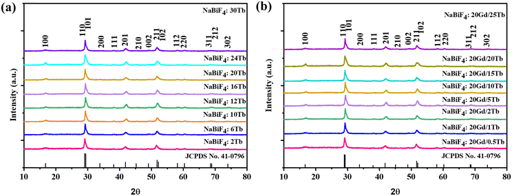
The X-ray diffraction (XRD) patterns revealed that all the resulting NBF:Ln NPs belonged to the hexagonal phase and no impurity peaks were observed (Fig. 1(a) and (b)).Fig. S1 (ESI†) depicts the PXRD pattern of the nanoparticles formed immediately after turbidity appearance, which matches with the hexagonal phase of NaBiF4. The PXRD pattern of the nanoparticles formed after 1 min of reaction matches well with the nanoparticles obtained after 30 min of reaction; hence, it confirms the formation of NaBiF4 immediately after mixing the solutions.
However, compared with the standard PDF card (PDF #41-0796), as the doping of Tb3+ concentration increases from 2% to 30% for NBF:x%Tb and from 0.5% to 25% for NBF:20% Gd,x%Tb, the positions of the diffraction peaks shift to large angles, which is caused by the decrease of the interplanar spacing (d). Since the radii of Tb3+ ions and Gd3+ ions are slightly smaller than the radius of Bi3+ ions, the substitution of Tb3+ ions and Gd3+ ions for Bi3+ ions causes lattice shrinkage (and hence the interplanar spacings), which further suggests that the rare-earth ions successfully occupy the lattice site of Bi3+. The peak observed around 41° of these patterns is magnified and shown in Fig. S2 (ESI†). It is clearly seen that the peak is shifting toward higher 2θ with increasing Tb3+ concentration. This is attributed to lattice shrinkage due to replacement of larger Bi3+ ions with smaller Tb3+ and Gd3+ ions as mentioned earlier. To confirm this fact, these XRD patterns are analysed by the Rietveld refinement method and the refinement plots are shown in Fig. S3 (ESI†). The refined unit cell parameters, typical structural parameters and residuals of the refinements are given in Table S1 (ESI†).
Moreover, when the dopant concentration increases from 2% to 24%, the XRD patterns of the samples remain in good agreement with those for hexagonal NaBiF4 nanocrystals.
Scanning electron microscopy (SEM) (Fig. 2(a)) and transmission electron microscopy (TEM) micrographs (Fig. 2(b)) indicate that the synthesized NPs exhibit a spherical shape. High-resolution TEM images show clear lattice fringes with a d-spacing of 0.305 nm corresponding to the (110) plane (Fig. 2(c)). The presence of Na, Bi, Gd, Tb, and F elements in the NPs was confirmed by energy-dispersive X-ray (EDX) spectra [Fig. S4(g), ESI†], and elemental mapping images [Fig. S4(a)–(f) and S4(b), ESI†] indicated a uniform distribution of these elements.
Gd/Tb co-doped systems have been broadly used to realize UV-excited downshifted emission, in which the input UV photons are absorbed by Gd3+ sensitizers and then transferred to Tb3+ activators. A high doping concentration of activators allows the harvesting of photon energy via energy transfer during UV excitation, but it also causes detrimental cross-relaxation and energy migration to surface quenchers. In our experimental results, we found that the optical characteristics between the UV-excited downshifted emission and the XEOL emission were significantly different.
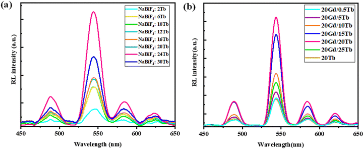
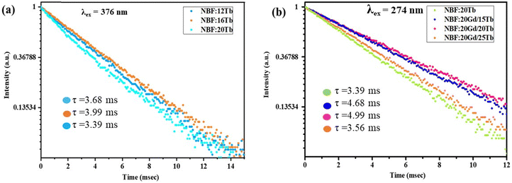
Emission spectra from the NBF:x%Tb nanoparticles (with varying concentrations of Tb) upon excitation at 376 nm are shown in Fig. 3(a). With the excitation of 376 nm UV light, NBF:x%Tb shows several narrow emission bands mainly in the green and orange part of the visible region due to the typical 5D4–7F5 (J = 3, 4, 5, and 6) transition of the Tb3+ ion. The emission spectrum consists of four sharp peaks at 490, 544, 590 and 621 nm and is attributed to the 5D4 → 7F6, 5D4 → 7F5, 5D4 → 7F4, and 5D4 → 7F3, transitions, respectively due to the Tb3+ ions present in the NBF lattice.42 These emission bands are dominated by the emission originating at 544 nm from the 5D4 → 7F5 transition. The optimal doping content of Tb3+ ions was only about 16 mol% and the emission intensity was enhanced about ∼3.8 times compared with that of 10 mol%. Integrated PL intensity profiles at various Tb3+ doping contents are shown in Fig. S5 (ESI†). The decrease in emission intensity beyond 16 mol% is attributed to concentration quenching. The radioluminescence spectrum of NBF:x%Tb and NBF:Gd,Tb nanoparticles upon X-ray excitation was recorded, as shown in Fig. 4(a) and (b). However, in the case of XEOL, the optimum doping concentration of Tb3+ ions was 24 mol% (Fig. 4(a)) and the XEOL intensity was enhanced by 3 times when increasing the Tb3+ ion dopant concentration from 2% to 24 mol%; then it started to decrease with a further increase in the Tb3+ ion dopant concentration to 30 mol%. According to the PL decay curves, the 16 mol% Tb3+ doped sample had a longer lifetime than the 12 and 20 mol% samples (Fig. 5(a)), supporting the efficient contribution due to radiative transition. The photoluminescence excitation spectra (Fig. S6, ESI†) of NBF:Gd,Tb correspond to 544 nm emission and consist of a sharp peak with a maximum at ∼274 nm along with less intense peaks. Peaks at about 273 and 312 nm are assigned to the Gd3+ transitions from the ground level 8S7/2 to excited levels 6IJ, 6PJ, respectively. Narrow peaks above 300 nm are assigned to intra-configurational f–f transitions of Tb3+ ions, i.e., 7F6 → 5D0,1 (317, 327 nm), 7F6 → 5G2–6 (341, 350, 357 nm) and 7F6 → 5D2,3 (368, 377 nm) transitions.
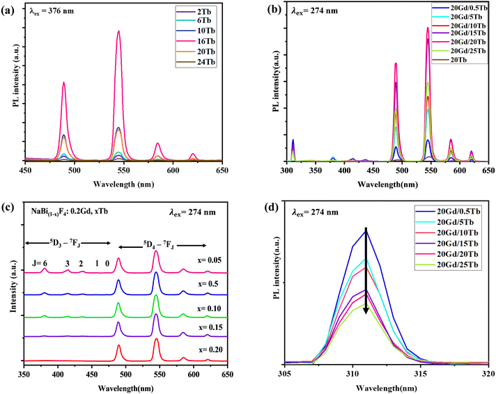 | ||
| Fig. 3 (a) PL spectra of NBF:x%Tb (x = 2–24%) under 376 nm excitation; (b) and (c) NBF:20Gd,x%Tb under 273 nm excitation; (d) PL emission spectra from Gd3+ ions corresponding to emission at 310 nm. | ||
To further investigate the energy transfer from Gd3+ to Tb3+ ions, the emission spectrum of NBF:20Gd3+,xTb3+ (0.5% ≤ x ≤ 25%) monitored at 274 nm was measured, as shown in Fig. 3(b)–(d). The emissions could be attributed to 5D3 → 7FJ (J = 2, 3, 4, 5 and 6) and 5D4 → 7FJ (J = 3, 4, 5 and 6) transitions of Tb3+ ions, among which the transition 5D4 → 7F5 leads to green emission at 544 nm. The 5D4 emission of Tb3+ increased, while the 5D3 emission decreased with an increase in the Tb3+ content, which is due to the cross relaxation between the 5D3 → 5D4 transition and 7F6 → 7F0 transition of Tb3+. The 5D4 emission of Tb3+ increased rapidly with an increase in the concentration of Tb3+. This is due to numerous factors along with the cross relaxation between the 5D3 and 5D4 levels since luminescence centres increase with the concentration of the Tb3+ ions in the host. The decreasing emission intensities from Gd3+ ions at 310 nm (Fig. 3(d)) with increasing Tb3+ ion content indicated that much more efficient energy transfer from Gd3+ to Tb3+ ions occurs in a sample. The highest PL intensity was observed for NBF:20Gd,20Tb nanoparticles. The PL decay curves suggested that the NBF:20Gd,20Tb sample exhibited a longer lifetime than that of NBF:20Tb, which confirms the efficient energy transfer from Gd3+ to Tb3+ ions [Fig. 5(a) and (b)].
Nonetheless, in our experimental results, the optical characteristics between the UV-excited downshifted emission and the XEOL emission were significantly different. The energy capture and transfer mechanisms were investigated to explain the different optical luminescence intensity variation trends under UV and X-ray excitation.
The proposed mechanism of X-ray scintillation in the lanthanide doped nanoscintillators is described below. The incident X-ray photons (<50 keV) first interact with all heavy elements present (Bi3+, Gd3+, and Tb3+) to generate hot electrons and deep holes, mainly through the photoelectric effect and the Compton scattering effect (Fig. 6). Subsequently, a large number of secondary electrons are produced via electron–electron scattering and the Auger process, resulting in the creation of charge carriers with significantly lower kinetic energy. These numerous charge carriers, including electrons and holes, are predominantly directed towards luminescence centers. To understand the process of electron population in the excited states of Tb3+, X-ray-excited optical luminescence (XEOL) intensities were measured for NBF:20Tb and NBF:20Gd/20Tb NPs under identical conditions. In comparison to NBF:20Tb nanoparticles, the XEOL intensity increased after doping with Gd3+ ions, as depicted in Fig. 4(b). This suggests that the Gd3+ 6P7/2 state has the ability to capture a portion of the secondary electrons and then transfer the energy to Tb3+:5D3 states to produce strong green emission upon X-ray radiation. The maximum XEOL intensity was seen in NBF:20Gd/20Tb and is also in accordance with the PL results (Scheme 1).
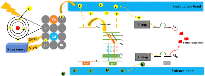 | ||
| Fig. 6 Proposed energy conversion and transport and luminescence mechanisms in the NBF:Gd/Tb nanoscintillator. | ||
A significant decrease in the luminescence persistence was observed and this is due to the generation of fluoride vacancies and interstitials as electron traps (E-traps) and hole traps (H-traps) due to elastic collisions between X-ray photons and fluoride ions. The captured secondary electrons in E-traps migrate to the conduction band and subsequently to activators, leading to radiative emission through electron–hole recombination. Compared to NaBiF4:24Tb, the afterglow was significantly quenched with doping Gd3+ (20 mol%) and Bi3+ (60 mol%) ions (Fig. S7, ESI†), confirming that both Gd3+ and Bi3+ ions could quench the afterglow. Owing to the elastic collision of large momentum X-ray photons with small fluoride ions, fluoride vacancies and interstitials are formed as electron traps (E-traps) and hole traps (H-traps), respectively. The secondary electrons captured by E-traps can escape over time to the conduction band followed by their migration to the activators; meanwhile, the trapped holes can also migrate toward the activators, leading to radiative emission via electron–hole recombination. For NaBiF4:20Gd/20Tb NPs, a significant portion of Bi3+ ions in the matrix facilitates energy migration from E-trap states to surface quenchers via the Bi3+ sublattice, reducing electron storage in the E-trap states and resulting in a substantial afterglow reduction. Additionally, the Gd3+ excited state competes with E-trap states for capturing secondary electrons, leading to a decreased electron population in the E-trap states and a subsequent reduction in afterglow (Fig. S8(c), ESI†).
The integral scintillation intensity of the NBF:20Gd/20Tb NSs was measured to be about 37.8% of that from the commercial CsI (Tl), which is much higher than the previously reported value of 11.5% [Fig. S8(b), ESI†]. The stability tests of the NBF:20Gd/20Tb NPs were conducted under continuous X-ray irradiation (Fig. S8(d), ESI†). The radioluminescence intensities of the NBF:20Gd/20Tb NPs show no obvious reduction after continuous X-ray exposure for 60 min, indicating excellent resistance to X-ray radiation damage [Fig. S8(d), ESI†].
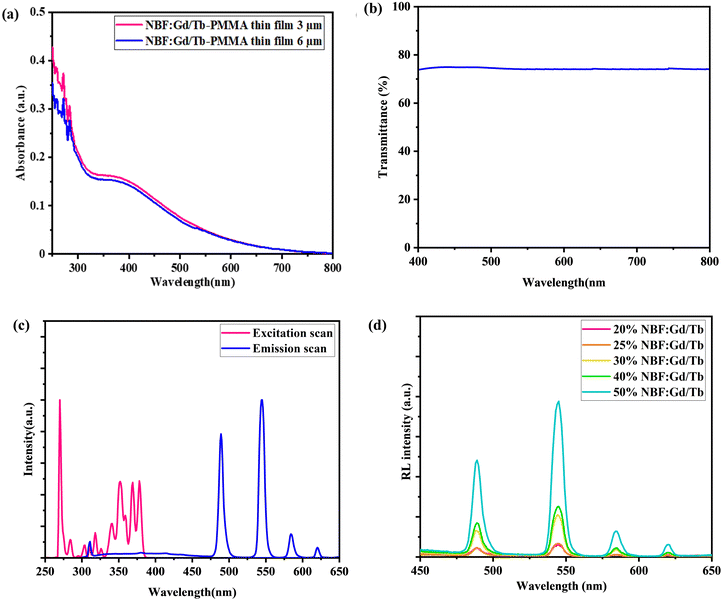
To explore the potential application of these NSs in X-ray imaging, uniform PMMA–NBF composite films were prepared. A uniform film with a thickness of ∼3.03 μm was prepared by blending NBF:20Gd/20Tb NPs with PMMA (Fig. 7(b)). The FE-SEM (Fig. 7(a)) and EDX images indicate uniformity and the presence of all the elements in the film (Fig. S9, ESI†). More importantly, this film is highly transparent in the measured wavelengths ranging from 400 to 700 nm (Fig. 8(b)), benefiting from the reduced light scattering and then a reduction in the signal cross-talk in the photodiode array, thus producing an improved image resolution. For application in radiography, it is important to optically characterize the NBF:Gd/Tb nanoparticles as well as the PMMA–NBF composite films.
 | ||
| Fig. 7 (a) FESEM image of a PMMA–NBF film and (b) cross-sectional FE-SEM image of a PMMA–NBF thin film. | ||
The optical characterization was carried out by recording the absorption spectra and the photoluminescence spectra. The absorption spectra of the NBF:Gd/Tb and PMMA–NBF:Gd/Tb composite films are compared in Fig. S8(a) (ESI†). All the samples exhibit absorption bands at 368, 377, and 486 nm, which can be attributed to the Tb3+ 7F6 → 5L10, 5D3, 5D4 transitions. Whereas, the bands peaking at ∼275 and ∼225 nm belong to the low spin-allowed (LS) 4f → 5d1 and 4f → 5d2 absorption transitions, respectively, in Tb3+. It is clear that there are additional peaks at about 250, 273, and 312 nm, which are assigned to the Gd3+ transitions from the ground level 8S7/2 to excited levels 6DJ, 6IJ, 6PJ, respectively. No additional bands were observed due to PMMA.42 The comparison between the absorption spectra of the PMMA–NBF:Gd/Tb composite films with varying thickness is shown in Fig. 8(a). No significant change in absorbance is observed with varying thickness of the film, indicating that the PMMA matrix is transparent to NBF:Gd/Tb emission and this confirms that thicker films can be used as imaging screens.
Fig. S10(a) (ESI†) shows the transmittance spectra of the prepared PMMA:NBF films with different thicknesses, 3 and 6 μm. It is observed that with an increase in the thickness of the PMMA:NBF film the transmittance was decreased and the corresponding image quality (resolution) became worse due to the increased light scattering from the NBF particles (Fig. S10(b), ESI†).
Fig. 8(c) shows the PL spectra of the PMMA–NBF:Gd/Tb composite film. The emission spectra of the composite films consist of an intense peak at 544 nm. This emission is due to the 5D4 → 7F5 transitions of Tb3+ ions present in the NBF lattice.18 This confirms that the luminescence property of the composite film is dominated by the inorganic component (NBF:Gd/Tb) and the organic polymer is transparent to this emission and it does not give any additional emission, nor does it affect the luminescence properties of NBF:Gd/Tb. The advantage of the green emission at 544 nm is that it can be directly coupled to a CCD camera that has its maximum sensitivity in this range for imaging applications.
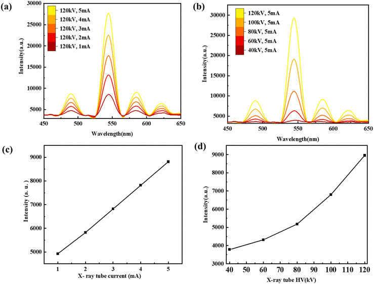
The scintillation and PL properties of the PMMA–NBF composite films were evaluated by measuring their luminescence characteristics. The main RL peak observed at 544 nm (Fig. 8(d)) closely resembles the PL peak and hence can be attributed to the Tb emission. The integrated XEOL intensity of the NBF:Gd/Tb as a function of X-ray tube voltage and tube current is shown in (Fig. 9(a) and (b)). An increase in the integrated RL intensity is observed initially with increasing voltage and then it starts saturating. The integrated XEOL intensity is linearly correlated with X-ray dose, which is in favour of high X-ray image contrast [Fig. 9(c) and (d)].
Fig. 8(d) shows the XEOL spectra of PMMA:NBF composite films at different loading percentages. XEOL spectra for all the films show peaks at 490, 544, 590 and 621 nm and are attributed to the 5D4 → 7F6, 5D4 → 7F5, 5D4 → 7F4, and 5D4 → 7F3, transitions, respectively, of Tb3+ ions present in the NBF lattice.18 The XEOL and PL (Fig. S11(a), ESI†) intensity increases on increasing the loading level of NBF due to the presence of more luminescent centres. Fig. S11(b) (ESI†) shows the transmission spectra of the PMMA:NBF film (thickness 3 μm) with different loading percentages. It is observed that with an increase in the loading percentage the transmittance decreases due to the increased scattering from the NBF particles.
Considering the requirements for high-quality X-ray imaging and high-sensitivity photoelectric conversion, strong RL and high transparency of PMMA–NBF:Gd,Tb composite films are expected. Therefore, the PMMA–NBF:Gd,Tb composite film was selected to demonstrate their practical application.
To further reveal the potential possibility of our prepared NBF:20Gd/20Tb nanoscintillator for practical X-ray imaging, its corresponding uniform film is employed as a nanoscintillator screen and a simple X-ray imaging system is setup (Fig. 10). The composite film was kept at the screen position and a direct image of the X-ray beam as well as the image shadow of the duplex wire was recorded using a commercially available CCD camera in the transmission mode. Fig. S12 (ESI†) shows the X-ray images recorded with PMMA:NBF (thickness 3 μm) films with different loading percentages. We observe that the brightness and the sharpness of the image increase with the loading from 20 to 50% (amount of NBF:Gd/Tb is 20% “by weight” to that of PMMA polymer). The best image is recorded for a 50% loaded film. As stated earlier, increasing the loading percentage of NBF beyond 50% also rendered brittleness to the films and generation of stress, which makes the films curl at the edges. The best results have been achieved in 50% loading (amount of NaBiF4: 20Gd/20Tb is 50% “by weight” to that of the PMMA polymer). A spatial resolution of 100 microns was achieved with the PMMA–NBF composite film using the standard line pair (Fig. 10(b)). The radiography image is of a duplex wire, imaged successfully by a PMMA–NBF-50 composite film with a spatial resolution of 100 microns (10 lp mm−1). We would like to add that this value is comparable to that for typical commercial CsI (Tl) scintillator40 (∼10 lp mm−1)-based X-ray imaging and much better than the resolution of 2.8 lines per mm reported for commercial Gd2O2S:Tb, GOS:Tb screens.41,42,44
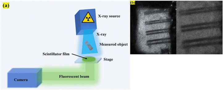 | ||
| Fig. 10 (a) X-Ray radiography setup consisting of an X-ray source, object, CCD camera, and the composite screen and (b) image formed by a duplex wire with a resolution of 100 microns. | ||
4. Conclusions
In summary, NBF:20Gd/20Tb NP was synthesized using the co-precipitation method at room temperature. These NSs showed strong XEOL intensity, excellent stability, and ultra-weak afterglow. The incorporation of Gd3+ ions enhanced the XEOL intensity of the NaBiF4:Tb NSs, indicating energy transfer from Gd3+ to Tb3+ ions. Moreover, by employing the highly transparent NBF:20Gd/20Tb film with a thickness of 3.03 μm as a nanoscintillator screen for XEOL imaging, a high spatial resolution of 100 microns was realized, which is comparable to the commercial CsI (TI) scintillator and much better than that of the commercial Gd2O2S:Tb, GOS:Tb scintillators employed for screens. Our results promote the development of a new generation of NSs, with low cost and high performance in the X-ray imaging field. Overall, this work represents a new direction for designing and developing Bi-based nanophosphors for rare earth luminescence upon X-ray excitation, and will lead the way to access broad use of these advanced bismuth-based NSs for X-ray detection and imaging applications.Conflicts of interest
The authors declare no competing financial interest.Acknowledgements
A. K. G. thanks the Department of Science & Technology (DST), Govt. of India for providing financial support. M. B. thanks CSIR and University at Buffalo for the support. We acknowledge Dr P. S. Sarkar from Technical Physics Division, BARC for his support in the measurement of X-ray imaging.References
- H. Wu, Q. Wang, A. Zhang, G. Niu, M. Nikl, C. Ming, J. Zhu, Z. Zhou, Y. Y. Sun, G. Nan, G. Ren, Y. Wu and J. Tang, One-Dimensional Scintillator Film with Benign Grain Boundaries for High-Resolution and Fast X-ray Imaging, Sci. Adv., 2023, 9 DOI:10.1126/sciadv.adh1789.
- S. Y. Yao, H. Li, M. Zhou, T. C. Wang, X. Yu, Y. S. Xu, J. H. Yi, J. B. Qiu, J. Yu and X. H. Xu, Visualization of X-Rays with an Ultralow Detection Limit via Zero-Dimensional Perovskite Scintillators, ACS Appl. Mater. Interfaces, 2022, 14, 56957–56962 CrossRef CAS PubMed.
- T.-C. Wang, S.-Y. Yao, S.-P. Yan, J. Yu, Z.-Y. Deng, A. N. Yakovlev, B. Meng, J.-B. Qiu and X.-H. Xu, High Thermal Stability of Copper-Based Perovskite Scintillators for High-Temperature X-Ray Detection, ACS Appl. Mater. Interfaces, 2023, 15, 23421–23428 CrossRef CAS PubMed.
- L. Lian, M. Zheng, W. Zhang, L. Yin, X. Du, P. Zhang, X. Zhang, J. Gao, D. Zhang, L. Gao, G. Niu, H. Song, R. Chen, X. Lan, J. Tang and J. Zhang, Efficient and Reabsorption-Free Radioluminescence in Cs3Cu2I5 Nanocrystals with Self-Trapped Excitons, Adv. Sci., 2020, 7, 2000195 CrossRef CAS PubMed.
- X. Wang, H. Shi, H. Ma, W. Ye, L. Song, J. Zan, X. Yao, X. Ou, G. Yang, Z. Zhao, M. Singh, C. Lin, H. Wang, W. Jia, Q. Wang, J. Zhi, C. Dong, X. Jiang, Y. Tang, X. Xie, Y. Yang, J. Wang, Q. Chen, Y. Wang, H. Yang, G. Zhang, Z. An, X. Liu and W. Huang, Organic Phosphors with Bright Triplet Excitons for Efficient X-Ray-Excited Luminescence, Nat. Photonics, 2021, 15, 187–192 CrossRef CAS.
- T. Ji, T. Wang, H. Li, Q. Peng, H. Tang, S. Hu, A. Yakovlev, Y. Zhong and X. Xu, Ce3+-Doped Yttrium Aluminum Garnet Transparent Ceramics for High-Resolution X-Ray Imaging, Adv. Opt. Mater., 2022, 10, 2102056 CrossRef CAS.
- J. Ma, W. Zhu, L. Lei, D. Deng, Y. Hua, Y. M. Yang, S. Xu and P. N. Prasad, Highly Efficient NaGdF4:Ce/Tb Nanoscintillator with Reduced Afterglow and Light Scattering for High-Resolution X-Ray Imaging, ACS Appl. Mater. Interfaces, 2021, 13, 44596–44603 CrossRef CAS PubMed.
- Y. C. Kim, K. H. Kim, D.-Y. Son, D.-N. Jeong, J.-Y. Seo, Y. S. Choi, I. T. Han, S. Y. Lee and N.-G. Park, Printable Organometallic Perovskite Enables Large-Area, Low-Dose X-Ray Imaging, Nature, 2017, 550, 87–91 CrossRef CAS PubMed.
- W. Ma, Y. Su, Q. Zhang, C. Deng, L. Pasquali, W. Zhu, Y. Tian, P. Ran, Z. Chen, G. Yang, G. Liang, T. Liu, H. Zhu, P. Huang, H. Zhong, K. Wang, S. Peng, J. Xia, H. Liu, X. Liu and Y. (Michael) Yang, Thermally Activated Delayed Fluorescence (TADF) Organic Molecules for Efficient X-Ray Scintillation and Imaging, Nat. Mater., 2022, 21, 210–216 CrossRef CAS PubMed.
- Y. Zhang, Light People: Professor Jianhua Jiang, Light: Sci. Appl., 2022, 11, 12 CrossRef CAS PubMed.
- L.-J. Xu, X. Lin, Q. He, M. Worku and B. Ma, Highly Efficient Eco-Friendly X-Ray Scintillators Based on an Organic Manganese Halide, Nat. Commun., 2020, 11, 4329 CrossRef CAS PubMed.
- I. V. Khodyuk, P. A. Rodnyi and P. Dorenbos, Nonproportional Scintillation Response of NaI:Tl to Low Energy X-Ray Photons and Electrons, J. Appl. Phys., 2010, 107, 113513 CrossRef.
- W. Ma, T. Jiang, Z. Yang, H. Zhang, Y. Su, Z. Chen, X. Chen, Y. Ma, W. Zhu, X. Yu, H. Zhu, J. Qiu, X. Liu, X. Xu and Y. (Michael) Yang, Highly Resolved and Robust Dynamic X-Ray Imaging Using Perovskite Glass-Ceramic Scintillator with Reduced Light Scattering, Adv. Sci., 2021, 8, 2003728 CrossRef CAS PubMed.
- E. Dieguez, L. Arizmendi and J. M. Cabrera, X-Ray Induced Luminescence, Photoluminescence and Thermoluminescence of Bi4Ge3O12, J. Phys. C: Solid State Phys., 1985, 18, 4777–4783 CrossRef CAS.
- J. K. Chen, N. Shirahata and H. T. Sun, Metal-free scintillators excite X-ray community, Nat. Photonics, 2021, 15, 171–172 CrossRef CAS.
- Q. Chen, J. Wu and X. Ou, et al., All-inorganic perovskite nanocrystal scintillators, Nature, 2018, 561, 88–93 CrossRef CAS PubMed.
- H. Chen, X. Sun, G. D. Wang, K. Nagata, Z. Hao, A. Wang, Z. Li, J. Xie and B. Shen, LiGa5O8:Cr-Based Theranostic Nanoparticles for Imaging-Guided X-Ray Induced Photodynamic Therapy of Deep-Seated Tumors, Mater. Horiz., 2017, 4, 1092–1101 RSC.
- R. Yasuda, M. Kataigiri and M. Matsubayashi, Influence of powder particle size and scintillator layer thickness on the performance of Gd2O2S:Tb scintillators for neutron imaging, Nucl. Instrum. Methods Phys. Res., Sect. A, 2012, 680, 139–144 CrossRef CAS.
- B. Yang, L. X. Yin, G. D. Niu, J. H. Yuan, K. H. Xue, Z. F. Tan, X. S. Miao, M. Niu, X. Du, H. S. Song, E. Lifshitz and J. Tang, Lead-Free Halide Rb2CuBr3 as Sensitive X-Ray Scintillator, Adv. Mater., 2019, 31, 1904711 CrossRef CAS PubMed.
- T. Jiang, Z. Chen, X. Chen, X. Chen, X. Xu, T. Liu, L. Bai, D. Yang, D. Di, W. E. I. Sha, H. Zhu and Y. M. Yang, Power Conversion Efficiency Enhancement of Low-Bandgap Mixed Pb–Sn Perovskite Solar Cells by Improved Interfacial Charge Transfer, ACS Energy Lett., 2019, 4, 1784–1790 CrossRef CAS.
- T. Jiang, Z. Chen, X. Chen, T. Liu, X. Chen, W. E. I. Sha, H. Zhu and Y. (Michael) Yang, Realizing High Efficiency over 20% of Low-Bandgap Pb–Sn-Alloyed Perovskite Solar Cells by In Situ Reduction of Sn4+, Sol. RRL, 2020, 4, 1900467 CrossRef CAS.
- Y. Gao, Z. Wei, P. Yoo, E. Shi, M. Zeller, C. Zhu, P. Liao and L. Dou, Highly Stable Lead-Free Perovskite Field-Effect Transistors Incorporating Linear π-Conjugated Organic Ligands, J. Am. Chem. Soc., 2019, 141, 15577–15585 CrossRef CAS PubMed.
- J. Qiu, H. Zhao, Z. Mu, J. Chen, H. Gu, C. Gu, G. Xing, X. Qin and X. Liu, Turning Nonemissive CsPb2Br5 Crystals into High-Performance Scintillators through Alkali Metal Doping, Nano Lett., 2024, 24, 2503–2510 CrossRef CAS PubMed.
- F. Wang and X. Liu, Upconversion Multicolor Fine-Tuning: Visible to Near-Infrared Emission from Lanthanide-Doped NaYF4 Nanoparticles, J. Am. Chem. Soc., 2008, 130, 5642–5643 CrossRef CAS PubMed.
- P. Huang, W. Zheng, S. Zhou, D. Tu, Z. Chen, H. Zhu, R. Li, E. Ma, M. Huang and X. Chen, Lanthanide-Doped LiLuF4 Upconversion Nanoprobes for the Detection of Disease Biomarkers, Angew. Chem., Int. Ed., 2014, 53, 1252–1257 CrossRef CAS PubMed.
- L. Lei, Y. Wang, W. Xu, R. Ye, Y. Hua, D. Deng, L. Chen, P. N. Prasad and S. Xu, Manipulation of time-dependent multicolour evolution of X-ray excited afterglow in lanthanide-doped fluoride nanoparticles, Nat. Commun., 2022, 13, 5739 CrossRef CAS PubMed.
- L. Lei, Y. Wang, A. Kuzmin, Y. Hua, J. Zhao, S. Xu and P. N. Prasad, Next generation lanthanide doped nanoscintillators and photon converters, eLight, 2022, 2, 17 CrossRef.
- L. Lei, M. Yi, Y. Wang, Y. Hua, J. Zhang, P. N. Prasad and S. Xu, Dual heterogeneous interfaces enhance X-ray excited persistent luminescence for low-dose 3D imaging, Nat. Commun., 2024, 15, 1140 CrossRef CAS PubMed.
- H. H. Gorris and O. S. Wolfbeis, Photon-Upconverting Nanoparticles for Optical Encoding and Multiplexing of Cells, Biomolecules, and Microspheres, Angew. Chem., Int. Ed., 2013, 52, 3584–3600 CrossRef CAS PubMed.
- J. Zhou, Q. Liu, W. Feng, Y. Sun and F. Li, Upconversion Luminescent Materials: Advances and Applications, Chem. Rev., 2015, 115, 395–465 CrossRef CAS PubMed.
- M. Bungla, P. Sharma, A. Shanavas and A. K. Ganguli, Methylene blue loaded K0.3Bi0.7F2.4:Yb,Er upconversion nanoparticles for near-infrared activated photodynamic therapy, New J. Chem., 2024, 48, 1800–1808 RSC.
- D. Chen, Y. Liang, S. Miao, X. Shan, X. Wang, W. Wang, Y. Zhang, J. Bi and D. Tang, Self-surfactant room-temperature synthesis of morphology-controlled K0.3Bi0.7F2.4 nanoscintillators, J. Mater. Chem. C, 2022, 10, 14296–14305 RSC.
- Y. Guo, J. Xie, M. Yu, W. Huang, H. Yang, X. Li, L. Wang and Q. Zhang, The enhanced up-conversion green by Yb–Mn dimer in NaBiF4:Yb3+/Er3+/Mn2+ for optical fiber temperature sensor, J. Alloys Compd., 2021, 888, 161497 CrossRef CAS.
- X. Gao, D. Ju, X. Sang, J. Yang, Y. Zhang and F. Song, Temperature-responsive NaBiF4:Yb3+,Er3+/Tm3+ based on non-thermally coupled levels, J. Lumin., 2023, 257, 119711 CrossRef CAS.
- L. Sun, NaBiF4-based hollow upconversion nanoparticles for temperature sensing, Light: Sci. Appl., 2022, 11, 257 CrossRef CAS PubMed.
- X. Zhang, J. Chen, Y. Min, G. B. Park, X. Shen, S. Song, Y. Sun, H. Wang, W. Long, J. Xie, K. Gao, L. Zhang, S. Fan, F. Fan and U. Jeong, Metabolizable Bi2Se3 Nanoplates: Biodistribution, Toxicity, and Uses for Cancer Radiation Therapy and Imaging, Adv. Funct. Mater., 2014, 24, 1718–1729 CrossRef CAS.
- P. Lei, R. An, X. Zhai, S. Yao, L. Dong, X. Xu, K. Du, M. Zhang, J. Feng and H. Zhang, Benefits of Surfactant Effects on Quantum Efficiency Enhancement and Temperature Sensing Behavior of NaBiF4 Upconversion Nanoparticles, J. Mater. Chem. C, 2017, 5, 9659–9665 RSC.
- M. Bungla, S. Chowdhari, M. Shanu, P. Pragya, V. Perumal, G. V. Prakash and A. K. Ganguli, NaBiF4:Yb3+,Tm3+ Submicron Particles as Luminescent Probes for in Vitro Imaging of Cells, Phys. Chem. Chem. Phys., 2023, 25, 6131–6141 RSC.
- P. Lei, R. An, S. Yao, Q. Wang, L. Dong, X. Xu, K. Du, J. Feng and H. Zhang, Ultrafast Synthesis of Novel Hexagonal Phase NaBiF4 Upconversion Nanoparticles at Room Temperature, Adv. Mater., 2017, 29, 1700505 CrossRef PubMed.
- J. H. Heo, D. H. Shin, J. K. Park, D. H. Kim, S. J. Lee and S. H. Im, High-Performance Next-Generation Perovskite Nanocrystal Scintillator for Nondestructive X-Ray Imaging, Adv. Mater., 2018, 30 DOI:10.1002/adma.201801743.
- P. Büchele, M. Richter, S. F. Tedde, G. J. Matt, G. N. Ankah, R. Fischer, M. Biele, W. Metzger, S. Lilliu, O. Bikondoa, J. E. Macdonald, C. J. Brabec, T. Kraus, U. Lemmer and O. Schmidt, X-Ray Imaging with Scintillator-Sensitized Hybrid Organic Photodetectors, Nat. Photonics, 2015, 9, 843–848 CrossRef.
- P. Du, Y. Hua and J. S. Yu, Room-temperature synthesis of near-ultraviolet light-excited Tb3+-doped NaBiF4 green-emitting nanoparticles for solid-state lighting, RSC Adv., 2018, 8, 26676–26681 RSC.
- R. An, P. Lei, P. Zhang, X. Xu, J. Feng and H. Zhang, Near-infrared optical and X-ray computed tomography dual-modal imaging probe based on novel lanthanide-doped K0.3Bi0.7F2.4 upconversion nanoparticles, Nanoscale, 2018, 10, 1394–1402 RSC.
- L. Chen, Y. Wu, H. Huo, B. Tang, X. Ma, J. Wang, C. Sun, J. Sun and S. Zhou, Nanoscale Gd2O2S:Tb Scintillators for High-Resolution Fluorescent Imaging of Cold Neutrons, ACS Appl. Nano Mater., 2022, 5, 8440–8447 CrossRef CAS.
Footnote |
| † Electronic supplementary information (ESI) available: Elemental mapping, EDX spectrum, PLE, PL spectrum, XEOL spectra, persistent luminescence decay curve and radioluminescence stability of NBF:20Gd/20Tb powder samples. See DOI: https://doi.org/10.1039/d4tc01543f |
| This journal is © The Royal Society of Chemistry 2024 |

