
 Open Access Article
 This Open Access Article is licensed under a Creative Commons Attribution-Non Commercial 3.0 Unported Licence
3D-(p/p/n) NiO/NiWO4/WO3 heterostructures for the selective detection of ozone†
Navpreet
Kaur
 * and
Elisabetta
Comini
* and
Elisabetta
Comini
SENSOR Laboratory, Department of Information Engineering (DII), University of Brescia, Via D. Valotti 9, Brescia 25133, Italy. E-mail: navpreet.kaur@unibs.it
First published on 8th August 2024
Abstract
We propose 3D branched-like NiO/NiWO4/WO3 nano-heterostructures for the selective detection of ozone (O3) at ppb levels, which is crucial for environmental and public health protection. These complex nano-heterostructures were fabricated using a combination of the vapor–liquid–solid and vapor–solid mechanisms, during which the reaction between NiO and WO3 leads to the formation of an intermediate seed, i.e., NiWO4. By controlling the charge transport within the nano-heterostructure through modulation of the operating temperature, sensors demonstrated highly selective sensing performances toward O3 compared to NiO and WO3 nanowire sensors. At 300 °C, a response as high as 4709 ± 9 was observed for 300 ppb of O3 gas. In fact, we were able to achieve high selectivity toward O3 compared to other highly reactive oxidizing compounds such as NO2. Due to their remarkable sensing performance, these heterostructures are leading candidates for the fabrication of future-generation miniaturized sensing devices for environmental and/or health monitoring.
Introduction
Improving the gas-sensing properties of metal oxides (MOXs) by fabricating heterostructures from two different materials is an innovative and efficient strategy.1–3 Heterostructures provide unique properties such as efficient charge carrier transport, large reaction surface, and superior gas sensing performance.4,5 However, constructing heterostructures using 1D-nanostructures such as nanowires (NWs) is a challenging task, but it opens new ways to improve the electronic properties of the materials at the nanoscale level. This novel idea brings two different 1D-nanostructured metal oxides into one single sensing platform through the formation of a heterojunction. Due to this junction formation, the Fermi levels of dissimilar metal oxides reach equilibrium, resulting in charge transfer and depletion region formation at the interface.6,7 In particular, 3D branched-like nano-heterostructures provide a surface with a substantial number of reactive sites and distinct charge carrier transport that enhance the sensitivity and selectivity and alter the operating temperature of the sensors compared to pristine material NWs.6,8In our previous report,8 we have seen that by controlling the charge transport in complex 3D p–p–n nano-heterostructures of NiO/NiWO4/WO3 with temperature, their sensing performance can be tuned toward oxidizing and reducing gases. In the current work, we focus on the selective detection of ozone (O3) using these nano-heterostructures. O3 is a crucial atmospheric component that plays a dual role, serving as both a beneficial shield against harmful ultraviolet radiation in the stratosphere and a pollutant at ground level.9,10 Ozone, a highly reactive molecule composed of three oxygen atoms, plays a dual role in our atmosphere.11,12 The ozone layer in the stratosphere shields the Earth from harmful ultraviolet (UV) radiation;13 ground-level ozone, primarily formed through photochemical reactions involving nitrogen oxides (NOx) and volatile organic compounds (VOCs), poses serious risks to human health and the environment.14 Exposure to elevated concentrations of ground-level ozone, even at parts per billion (ppb) levels, can result in adverse health effects, including respiratory problems, exacerbation of asthma, and cardiovascular issues.15–17 Therefore, the development of sensitive and selective ozone-sensing technologies is of paramount importance for environmental monitoring and public health protection.
In this work, we presented 3D-(p/p/n) nano-heterostructures for the detection of ozone at ppb levels. The core NiO nanowires were fabricated using the vapor-phase growth method via the vapor–liquid–solid (VLS) mechanism. WO3 was used as the secondary MOX, grown in the form of nanowires using the same technique via the vapor–solid (VS) mechanism onto NiO NWs. Intermediate growth of the ternary material (nickel tungstate NiWO4) was observed as seed formation on top of NiO NWs prior to the WO3 NWs creating branch-like heterostructures of NiO/NiWO4/WO3 (NWO). Afterward, a set of conductometric sensing devices based on pristine NiO and heterostructure sensors were prepared and tested for different concentrations of oxidizing and reducing compounds mainly focusing on the selective detection of ozone. The fabricated NWO heterostructure sensors exhibit higher sensitivity and selective behavior towards ozone even at ppb levels.
Experimental
Growth and characterization of NWO 3D-heterostructures
Polycrystalline alumina substrates 2 mm × 2 mm (Kyocera, Japan, with 99% purity) were used to fabricate the nanostructures. Before deposition, all substrates underwent ultrasonic cleaning with acetone and were subsequently dried with synthetic air. An ultrathin layer of the Au catalyst was deposited onto the Al2O3 substrates using RF magnetron sputtering (Kenotec Sputtering system, Italy). The deposition of Au was carried out at a power of 70 W with an Ar flow rate of 7 sccm at a pressure of 5 × 10⁻³ mbar for 5 seconds.For the core of the 3D-heterostructures, the NiO nanowires were fabricated using a tubular furnace by employing the vapor–liquid–solid (VLS) growth mechanism. The growth process was initiated at an evaporation temperature for the NiO powder (Sigma-Aldrich, 99% purity, CAS number: 1313-99-1) of 1400 °C, with an Ar flow rate of 100 sccm at a pressure of 1 mbar. The Au-catalyzed Al2O3 substrates were maintained at a temperature of 930 °C, and the deposition time was set for 15 minutes.18 After the fabrication of the core NiO NWs, the secondary material WO3 was used to fabricate small nanowires directly onto the NiO nanowires via the vapor–solid (VS) growth mechanism. The source material, WO3 powder (Sigma-Aldrich, 99% purity, CAS number: 1314-35-8), was heated up to 1100 °C, while the substrates with NiO nanowires were placed at a lower substrate temperature of 580 °C. During the deposition process, the argon flow was maintained at 100 sccm, and the pressure was held at 1 mbar, with a deposition time of 15 minutes.
The final 3D-heterostructures consisted of a long core of NiO NWs followed by the formation of the NiWO4 seed on the top and afterward the formation of small WO3 nanowires. During the process of WO3 NW growth, as the vapors of WO3 reach the surface of NiO NWs a reaction occurs, resulting in the formation of a ternary phase NiWO4. The well-known phase transition diagram of N–W–O suggested that at elevated temperatures of around 680 °C (pressure = 1 atm), the W–O system consists of different phases like WO2, WO2.9, and WO3.19 Moreover, in the presence of Ni and oxygen, these phases transit to the formation of the most stable phase of NiWO4.19 Thus, under the given experimental conditions, the binary components of NiO and WO3 first lead to the formation of a seed of NiWO4 as long as the WO3 vapors were able to reach the NiO surface. Afterward, further incoming WO3 vapors are not able to reach the NiO surface and the seed acts as a nucleation site for the growth of WO3 NWs resulting in the final 3D-heterostructures of NiO/NiWO4/WO3 (p/p/n).
The final heterostructure morphology was investigated using a field-emission scanning electron microscope (FE-SEM, model LEO 1525, ZEISS). The detailed investigation of pristine NiO NWs and 3D-heterostructures using GI-XRD, HR-TEM, RAMAN, and XPS has been provided in our previous article.8
Fabrication of gas sensing devices and electrical measurements
The conductometric sensing devices were fabricated by DC magnetron sputtering using NWO 3D-heterostructures and NiO NWs as the active transduction material. First, on the top of nanostructures, Pt interdigitated electrodes (IDEs) were deposited, and a platinum heater on the backside of the Al2O3 substrate. The complete process consists of deposition of the TiW adhesion layer using DC magnetron sputtering (70 W, Ar plasma, 100 nm, 300 °C, ≈5.3 × 10⁻³ mbar) followed by Pt electrodes, using the same parameters used for the adhesion layer (thickness ≈ 1 μm). The final devices were mounted on the transistor outline (TO) packages using electro-soldered gold wires.The conductometric response of the fabricated heterostructure based sensors was investigated using a flow-through technique.20 A custom stainless-steel chamber (1 L volume) located inside a climatic chamber (Angelantoni, Italy, model MTC 120) set at 20 °C was used to investigate the sensor response toward different gases. To simulate real ambient conditions, all the measurements were performed at a relative humidity of 50% with a constant synthetic air flow of 200 sccm. The atmosphere composition was controlled using mass flow controllers (MKS, Germany), mixing flows coming from certified gas bottles (SOL, Italy) containing a precise concentration of target analytes diluted in synthetic air. A constant bias of 1 V was applied to the sensing material to measure the output signal, recorded using a picoammeter (Keithley, USA). All the sensors were thermally stabilized at a desired temperature for 6 hours before starting the sensing measurement. The response was calculated by the variation of the conductance using the following formulas, for a p-type metal oxide under exposure to an oxidizing gas,21
 | (1) |
 | (2) |
| Response = A(gas concentration)B | (3) |
Results and discussion
The morphology of the nanostructures was examined using FE-SEM. The bare NiO samples (Fig. 1(a) and (b)) on alumina substrates show a dispersed and uniform nanowire structure with diameters ranging from 10 to 70 nm and lengths along with a few large structures. In Fig. 1(c) and (d), the morphology of the heterostructure illustrates the small WO3 nanowires growing on top of each core NiO nanowire, resulting in the formation of 3D-branch-like nanostructures comprised of three different materials NiO (core), NiWO4 (seed) and WO3 (secondary NWs).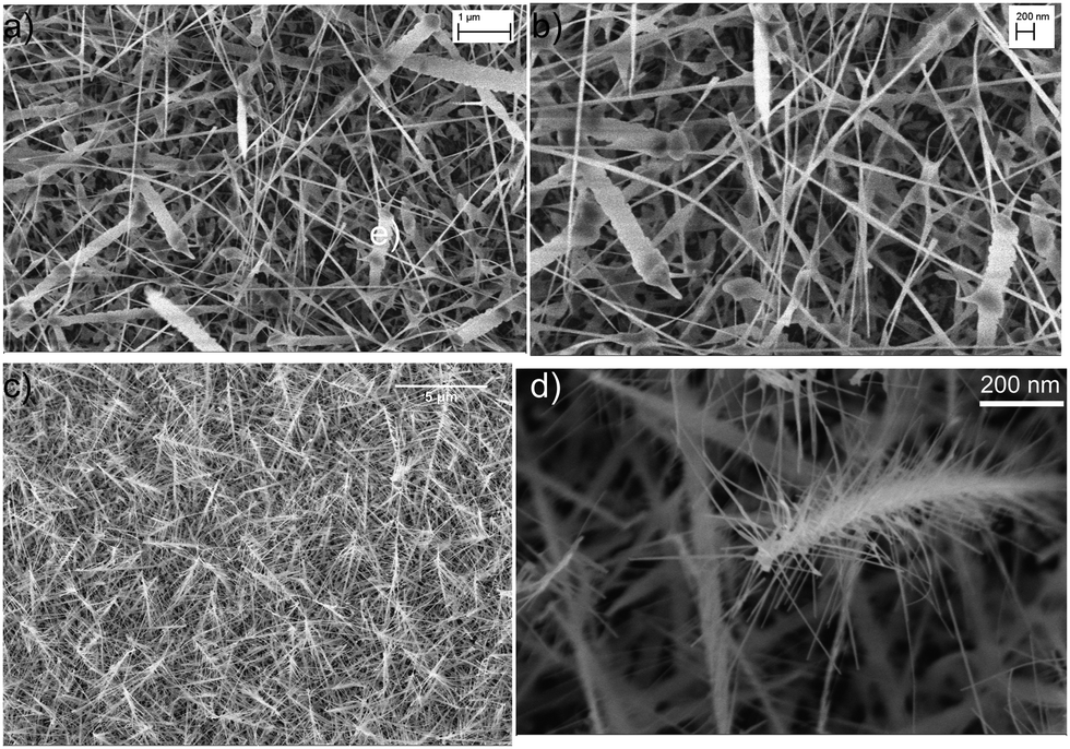 | ||
| Fig. 1 (a) and (b) SEM images of NiO nanowires grown at an evaporation temperature of 1400 °C, a pressure of 1 mbar, and 100 sccm argon flow using alumina substrates with the Au catalyst substrate at a temperature of 930 °C. (c) and (d) SEM images of NWO heterostructures grown at an evaporation temperature 1100 °C, a pressure of 1 mbar, and 100 sccm argon flow using alumina substrates with the Au catalyst substrate at a temperature of 580 °C. | ||
Gas sensing performance
The sensing performance of the fabricated NWO heterostructures and pristine NiO NWs was tested for different concentrations of ozone (50, 50, 150 and 300 ppb) at different temperatures (200, 300, 400, and 500 °C). Fig. 2(a)–(d) show the isothermal dynamic-transient response of NWO heterostructures compared to that of the NiO NWs at temperatures of 500, 400, 300 and 200 °C, respectively, and at a relative humidity level of 50%. Evidently, the baseline resistance of the NWO heterostructures is higher than that of the NiO NW sensors at all the operating temperatures. Specifically, the drop in the conductance baseline is near to one order of magnitude at a lower temperature (200 °C). The increased electrical resistance observed in NWO heterostructures is attributed to the built-in potential at the two interfaces (depletion region): one at the junction of NiO/NiWO4 (p/p) and the other at the junction of NiWO4/WO3 (p/n). The charge transport mechanism in NWO heterostructures will be discussed in detail later. | ||
| Fig. 2 Dynamic response curves of NiO and NWO sensing devices toward ozone gas (50, 50, 150, and 300 ppb) at temperatures of (a) 500 °C, (b) 400 °C, (c) 300 °C, and (d) 200 °C. All the measurements were performed at a relative humidity of 50% at 20 °C. | ||
Furthermore, the dynamic response of both NiO and NWO sensors shows an increase in electrical conductance under exposure to an oxidizing compound like ozone. This is the standard behavior of a p-type metal oxide sensor when exposed to an oxidizing analyte. This confirms that the hole is acting as the majority charge carrier in the heterostructure, which is due to the presence of two p-type metal oxide semiconductors (NiO and NiWO4) in the heterostructure system. The pristine NiO sensor shows low to no response when operated at a temperature of 500 °C compared to the NWO heterostructures. However, the dynamic response starts to increase at lower temperatures, with the highest dynamic response at 300 °C. Hence, 300 °C is the optimal working temperature for both the sensors. On the other hand, at lower temperatures such as 200 °C, both NiO and NWO sensors showed a significant response towards the O3; however, the heterostructure sensor dynamic kinetics are much faster. The NiO sensors show a lower recovery rate compared to the NWO sensors. Furthermore, the response values were calculated from eqn (1) and (2). Fig. 3(a) reports the calculated response values of NWO and NiO sensors at different operating temperatures towards 300 ppb of O3. The response of NWO sensors is comparably higher than that of NiO at temperatures of 200, 300, and 400 °C, while exhibiting comparable values at 500 °C. Evidently, at the optimal working temperature (300 °C), the response of NWO sensors is 10 times higher compared to that of the pristine NiO NW sensors.
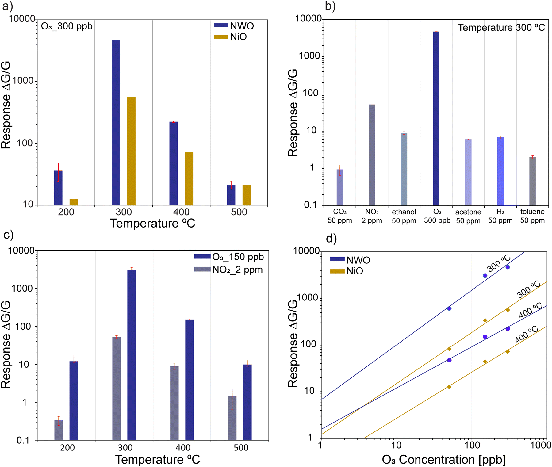 | ||
| Fig. 3 (a) Temperature dependence responses of the NWO heterostructure and NiO sensors towards 300 ppb of O3. (b) Response of the NWO heterostructure towards different interfering gases, ethanol (50 ppm), CO (50 ppm), NO2 (2 ppm), H2 (50 ppm), acetone (50 ppm), and toluene (50 ppm) with O3 (300 ppb) at an optimal working temperature of 300 °C. (c) Temperature dependence comparison of NWO heterostructure sensors towards O3_150 ppb and NO2_2 ppm in the temperature range from 200 to 500 °C. (d) Calibration plot for the NWO and NiO sensors toward different concentrations of O3 (50, 150, and 300 ppb) at temperatures of 300 °C and 400 °C. | ||
Furthermore, the sensing performance of NWO sensors was tested towards different reducing and oxidizing gas analytes at their optimal working temperatures. Fig. 3(b) reports the response of NWO sensors towards various gases such as hydrogen (50 ppm), CO (50 ppm), NO2 (2 ppm), ethanol (50 ppm), acetone (50 ppm), and toluene (50 ppm) at 300 °C. Different concentrations of the gases were chosen according to their exposure limits according to the European Union (EU) Air Quality Standards.23 For instance, testing at very high concentrations, such as 50 ppm of NO2 and O3, would not be significant for real-world conditions. According to the European Union (EU) Air Quality Standards, the permissible exposure limit for ozone is 0.1 ppm, with guidelines from organizations like the World Health Organization (WHO). Testing ozone at 50 ppm would not reflect practical exposure scenarios and thus would not be meaningful. Clearly, as shown in Fig. 3(b), the sensors showed the highest response towards ozone compared to the other analytes, proving their selective behavior towards ozone.
Investigating the selectivity of the sensors toward two major oxidizing gases like NO2 and O3 is very important. In Fig. 3(c), the response of the NWO sensors was compared at a range of temperatures from 200 to 500 °C towards 2 ppm of NO2 and 150 ppb of O3. Fig. 3(c) clearly shows that the NWO heterostructure sensors are more sensitive and selective towards O3 at all the operating temperatures. In particular, the response of NWO sensors is almost 59 times higher towards O3 compared to that of NO2 sensors at 300 °C. Fig. 3(d) reports the calibration curves of NWO and NiO sensors, i.e., response versus concentration, for O3 (50, 150 and 300 ppb) at 300 °C and 400 °C. The calculated coefficients with power fitting (eqn (3)) of the curve and detection limits for both sensors are reported in Table S1 in the ESI.† Considering the minimum response of 1, the detection limits of NWO sensors were found to be 0.19 and 0.59 ppb at 300 and 400 °C, respectively, indicating that the NWO heterostructure sensors are highly sensitive under the given operating conditions.
Additionally, Fig. 4(a)–(f) compare the response dynamics and values under optimal working conditions towards O3 for NWO heterostructure sensors with the host NiO NWs and to our previously reported WO3 nanowires17 fabricated by using the VLS mechanism. The response dynamics of WO3 follow an opposite trend compared to the NWO and NiO sensors due to its n-type semiconducting behavior.
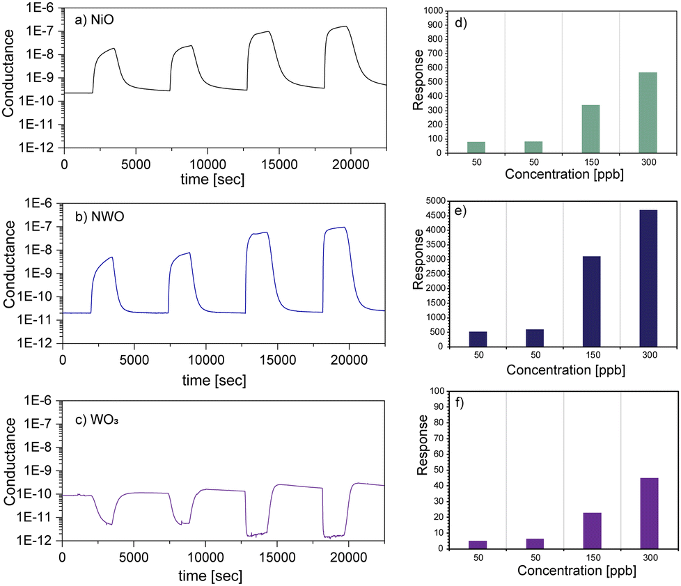 | ||
| Fig. 4 Dynamic response curves of NiO (a), NWO (b), and WO3 (c) sensing devices toward ozone gas (50, 50, 150, and 300 ppb) at 300 °C. Response curves of NiO (d), NWO (e), and WO3 (f) with respect to the concentration of O3 at 300 °C. | ||
Due to the electron-capturing nature of ozone, when it interacts with the surface of WO3 NWs, the concentration of majority charge carriers (electrons) decreases and in turn decreases the conductance of the WO3 sensor (Fig. 4(c)). This is a typical behavior of an n-type metal oxide semiconductor upon exposure to an oxidizing compound. Evidently, WO3 sensors exhibit the lowest sensing performance compared to the pristine NiO and NWO sensors (Fig. 4(d)–(f)). The highest response was found in the order of 10, 100 and 1000 for WO3, NiO and NWO 3D-heterostructure sensors, respectively. These results prove that integrating a sensing platform consisting of different materials in the form of nanostructures enhances the sensing performance. Finally, the calculated response/recovery time of the NWO heterostructures is presented in Table S1 (ESI†). Moreover, all fabricated sensors demonstrated good repeatability of the sensor signal, as presented in the statistical data. Additionally, Fig. S2 (ESI†) shows that the NWO heterostructure sensing device maintained a stable response even after three months from the initial measurements at 300 °C towards 150 ppb. The variation in the response of the sensors to ozone was less than 20%.
Furthermore, a comparison of the sensing performance of the NWO nano-heterostructure sensors with the literature is presented in Table S2 (ESI†). Drawing direct comparisons between our fabricated sensors and existing data poses challenges, as no similar type of heterostructure has been previously tested for ozone detection. However, compared to sensors based on bare and modified WO324,25 and NiO26 nanostructures, the NWO sensors exhibited superior performance. For instance, compared to other reported heterostructures such as In2O3/ZnO,27 although their operating temperature is lower, their response is around 6.7, which is significantly lower. Additionally, for heterostructures based on V2O5 NWs and TiO2,28 despite having the same operating temperature as reported for NWO heterostructures, the response is much lower (1.4), even at a higher concentration of O3 (1 ppm). Furthermore, L. Shao et al.29 reported an ozone sensor based on Zn:MoS2 nanosheets, which offers the advantage of room temperature operation. However, testing such a high concentration of O3 (5000 ppb) with a response lower than 1 has very little significance for real-time sensing. All the aforementioned comparisons, along with additional reports from the literature, are presented in Table S2 (ESI†).
Charge transport properties of NWO heterostructures
Before we go into the details of the sensing mechanism in NWO heterostructures, it is important to discuss their charge transport properties. It is a well-known fact that the chemisorption of oxygen ions on the surface of MOXs determines their charge transport properties when operated in air. Specifically, the chemisorption of oxygen ions on the surface of p- and n-type MOXs extracts electrons and forms a core–shell structure.30 In particular, a hole accumulation layer (HAL) around the resistive core and an electron depletion layer (EDL) around the conducting core are formed on the p- and n-type MOXs, respectively, as shown in Fig. 5(a) and (b). The formation of the HAL in p-type (NiO) MOXs increases their conductivity, while the conductivity of n-type MOXs (WO3) falls due to the formation of the EDL.31 On the other hand, NWO is a double junction device with the n/p/p configuration in which the conduction is controlled by the holes due to its dominating p-character.8 Specifically, two interfaces or junctions i.e. one between WO3/NiWO4 (n–p) and the second at NiWO4/NiO (p–p) are formed (Fig. 5(c)). In a vacuum, an interfacial potential barrier is formed at both interfaces due to the diffusion of charge carriers. The existence of these interface barriers in the heterostructure is the main reason behind their lower conductance from the NiO NWs. Furthermore, when NWO is operated in air, the chemisorption of oxygen ions leads to the formation of an EDL on the WO3 surface, while a HAL will be formed on NiO and NiWO4 surfaces. With the increase in the operating temperature, the charge carriers (electrons and holes) gain enough energy and start crossing both potential barriers, leading to the phenomenon of electron–hole recombination especially at the WO3/NiWO4 interface.8 The rate of recombination is increased with an increase in temperature in which electrons from WO3 are consumed significantly. Meanwhile, the density of holes is only slightly affected due to the dominating p-character of NWO. In fact, as the temperature increases, more and more holes are injected from NiO and NiWO4 and hence start dominating the overall p-type character of NWO. This also implies that, at 300 °C, a high density of electrons will be present in the NWO compared to at 400 °C and the density progressively decreases due to the electron–hole recombination as the temperature increases up to 500 °C.8 The whole phenomenon is pictorially depicted in Fig. 5(c). On the other hand, at 200 °C, the NWO heterostructure showed highly resistive behavior (see the dynamic response in Fig. 2(d)) and the charge transport is mainly controlled by the built-in potential at the two interfaces. It should be noted that the overall characteristics of the NWO heterostructure is always p-type due to the presence of two p-type materials, i.e. NiO and NiWO4. This has already been indicated by the sensing data shown in Fig. 2, in which the conductivity of NWO heterostructures increases upon interacting with oxidizing compounds like O3, which is a typical p-type MOX semiconductor behavior.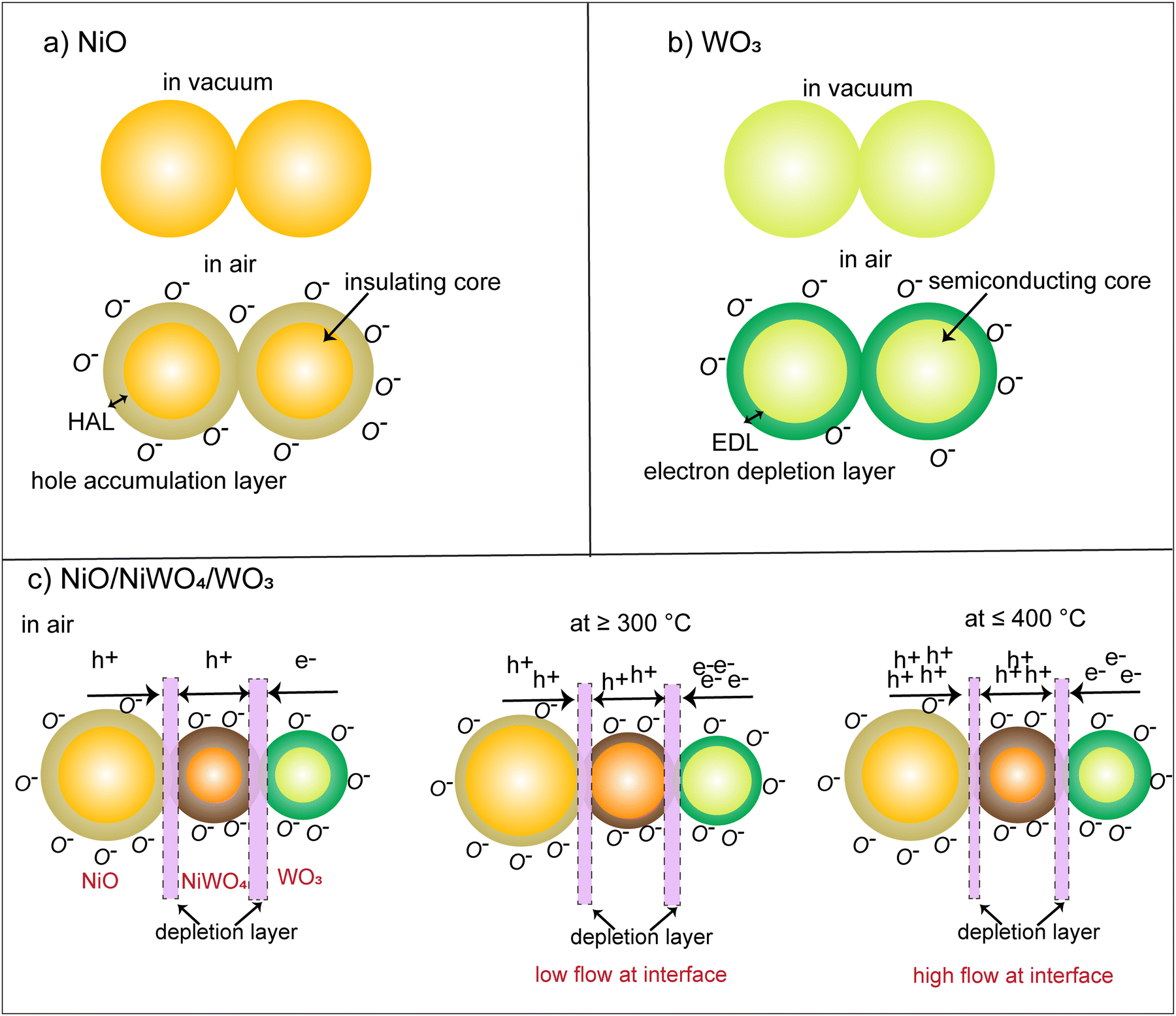 | ||
| Fig. 5 (a) The effect of chemisorption on the conductance of NiO, (b) WO3 and (c) NiO/NiWO4/WO3 heterostructures. | ||
Sensing mechanism
As mentioned earlier, the gas sensing properties of MOXs are determined by the chemisorbed oxygen ions whose density and types vary with temperature.31 Specifically, in the temperature range from 100 to 300 °C, the chemisorbed oxygen ions are in the form of O−, which further changes to O2− at temperatures >300 °C via capturing the electrons from the surface of MOXs. To understand the ozone interaction mechanism with the p-type MOX like NiO, let us first discuss the properties of O3. Ozone is a powerful oxidizing agent and a highly unstable gas molecule. Indeed, O3 possesses a higher electron affinity EA = 2.14 ± 0.15 eV (ref. 32) compared to chemisorbed oxygen ions (EA = 0.43 eV),33 thus exhibiting a higher tendency to extract electrons deep from the surface of NiO NWs. Moreover, O3 has a distinct dipole moment due to its molecular structure. In its configuration, the central atom carries a positive charge, while the surrounding atoms hold a negative charge.34 When NiO NWs are exposed to O3, the central positive atom extracts electrons from NiO, leading to the generation of free holes (wider than the thickness of the HAL), and increasing their conductance (see the dynamics in Fig. 2). The overall reaction of O3 with NiO NWs is as follows:| O3(gas) → O3(surf) + e− → O2(gas) + O−(ads) | (4) |
The above relationship shows that the capturing of electrons by surface-adsorbed O3 leads to the formation of O− ions and the release of oxygen gas. Fig. 6(a) depicts the different stages in which NiO NWs are in air and exposed to ozone.
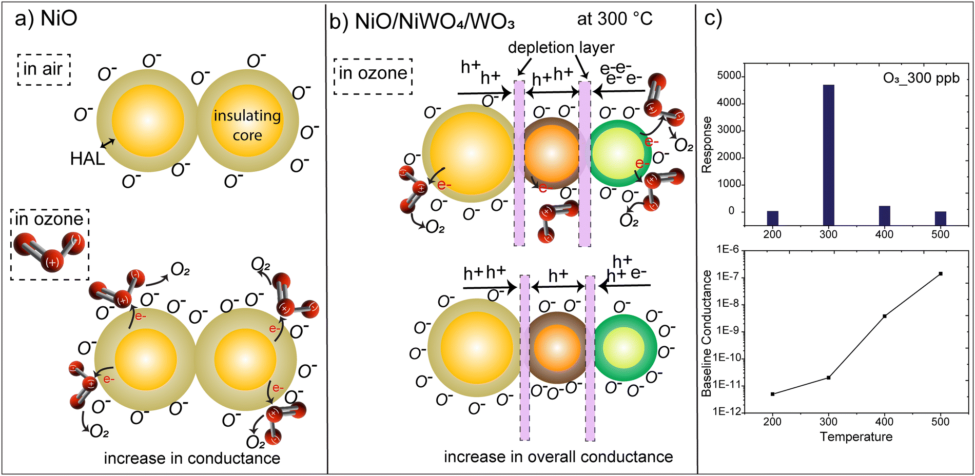 | ||
| Fig. 6 (a) Ozone sensing mechanism of pure NiO nanowires. (b) Ozone sensing mechanism of the NWO heterostructure sensor system. (c) Variation of the response and baseline conductance of the NWO heterostructure with respect to the applied temperature. | ||
In the case of NWO heterostructure sensors, different factors are involved behind their superior performance. The very first reason is that the 3D nano-heterostructure provides a significantly higher reactive surface area for O3 in comparison to 1D-NiO NWs. The symmetry of these heterostructures is also highly important to consider when discussing their performance. Using WO3 as a secondary material on the core of NiO provides a highly electron-rich material on the outer surface of the whole heterostructure system. Furthermore, the temperature-dependent response of NWO heterostructures can be explained based on the charge transport mechanism described earlier. At 300 °C, the density of electrons is higher compared to higher temperatures due to the electron–hole recombination mechanism, as shown in Fig. 6(b). This can also be seen from the baseline conductance of NWO sensors in air (Fig. 6(c)) which is three times higher at 400 °C than at 300 °C. Due to the thermal excitation at higher temperatures, the electron–hole recombination through the different interfaces increases, leading to a higher conductance resulting in the reduction of the density of free electrons. Thus, when NWO heterostructures are exposed to O3 at 300 °C, it is absorbed on the surface. These adsorbed O3 then dissociate and capture bound electrons from the surface of the heterostructure that results in the formation of O− species and the release of O2 gas. On the other hand, at 200 °C, the NWO heterostructure is apparently highly resistive (Fig. 6(c)), thus exhibiting poor sensing performance, but retains a higher response value in comparison to NiO NWs due to the presence of n-type WO3 and enhanced reactive sites in heterostructures.
Furthermore, even though both O3 and NO2 are oxidizing and highly reactive agents, the NWO heterostructure exhibited better performance toward O3. The answer to this question lies in their molecular structure that highly affects the reaction mechanism. Ozone is a triatomic molecule with three oxygen atoms arranged in a O–O–O manner creating an overall bent molecular geometry, with an angle of approx. 116° between the oxygen atoms.34,35 On the other hand, in the case of NO2, the diatomic molecule consists of one nitrogen atom and two oxygen atoms, resulting in a linear molecular geometry.36,37 Comparing both, the O3 is much more reactive due to the presence of three oxygen atoms that provide a higher degree of molecular strain leading to its high reactivity and is prone to undergo chemical reactions in the presence of other substances and with the metal oxide surface. Thus, the oxidizing potential of O3 is much higher than that of NO2, as it can readily react with the MOX surface and lead to the formation of adsorbed oxygen species. It is important to note that these two are gaseous pollutants with similar chemical properties, making it difficult to differentiate between them using traditional sensing MOX sensors. However, using advanced tailored heterostructures offers a promising solution, enabling the development of highly sensitive and selective sensors capable of distinguishing between different analytes with higher precision.
Conclusions
A novel highly selective ozone sensor was fabricated based on complex NiO/NiWO4/WO3 heterostructures. The NWO heterostructures were successfully synthesized using the single vapor-phase growth method employing a two-step growth technique. In the first step, NiO NWs were grown directly on the Au-catalysed alumina substrate using the VLS mechanism. Secondly, the small WO3 NWs were grown directly on the NiO core via the VS mechanism from a seed of the ternary material NiWO4, creating 3D branch-like nano-heterostructures. Furthermore, the fabricated NWO sensors exhibited superior performance in comparison to pristine NiO and WO3 NWs towards the detection of ozone at the ppb level. In particular, the heterostructure sensors demonstrated a higher and more selective response at 300 °C towards ozone compared to other oxidizing and reducing gas analytes. The main reason behind the superior performance is attributed to the formation of different interfaces between the different MOXs (p/p of NiO/NiWO4 and p/n of NiWO4/WO3). By controlling the charge carrier flow and density through these interfaces with applied temperature, the sensor exhibited a selective response towards O3 at 300 °C. In particular, the presence of WO3 provides free electrons on the surface of heterostructures, which makes them more reactive and selective towards an oxidizing gas like O3. Additionally, fabricated sensors based on 3D nano-heterostructures provide larger reactive surface areas and more reactive sites compared to the pristine NW sensors, leading to their enhanced and superior sensing performance. Finally, the NWO heterostructure sensor exhibited a response value of 4705 ± 9 towards 300 ppb of ozone, with a detection limit of 0.19 ppb at 300 °C. This makes them promising candidates for advancing cutting-edge environmental/health monitoring technologies.Author contributions
Navpreet Kaur: conceived the idea, planned the work, did all the experiments and data analysis, and wrote the manuscript. Elisabetta Comini: as the Head of the sensor lab supervised, provided funding for the research work, and edited the manuscript.Conflicts of interest
There are no conflicts to declare.Acknowledgements
This study was carried out within the MOST – Sustainable Mobility National Research Center and received funding from the European Union Next-Generation EU (PIANO NAZIONALE DI RIPRESA E RESILIENZA (PNRR) – MISSIONE 4 COMPONENTE 2, INVESTIMENTO 1.4 – D.D. 1033 17/06/2022, CN00000023), Spoke 5 “Light Vehicle and Active Mobility”. This manuscript reflects only the authors’ views and opinions, neither the European Union nor the European Commission can be considered responsible for them.References
- D. R. Miller, S. A. Akbar and P. A. Morris, Sens. Actuators, B, 2014, 204, 250–272 CrossRef CAS.
- F. J. Meng, R. F. Xin and S. X. Li, Materials, 2023, 16, 263 CrossRef.
- M. W. Alam, P. Pooja, M. Aamir, B. Souayeh, S. Mushtaq, M. S. Khan, M. N. Amin, K. Khan and S. Shajahan, Membranes, 2022, 12, 555 CrossRef CAS.
- D. Zappa, V. Galstyan, N. Kaur, H. M. M. Munasinghe Arachchige, O. Sisman and E. Comini, Anal. Chim. Acta, 2018, 1039, 1–23 CrossRef CAS PubMed.
- A. Singh, S. Sikarwar, A. Verma and B. Chandra Yadav, Sens. Actuators, A, 2021, 332, 113127 CrossRef CAS.
- N. Kaur, D. Zappa, M. Ferroni, N. Poli, M. Campanini, R. Negrea and E. Comini, Sens. Actuators, B, 2018, 262, 477–485 CrossRef CAS.
- N. Kaur, E. Comini, N. Poli, D. Zappa and G. Sberveglieri, Procedia Eng., 2016, 168, 1140–1143 CrossRef CAS.
- N. Kaur, D. Zappa, V.-A. Maraloiu and E. Comini, Adv. Funct. Mater., 2021, 2104416 CrossRef CAS.
- Z. Zhu, J. L. Chang, C. H. Wu, T. L. Chou and R. J. Wu, Sens. Actuators, B, 2016, 232, 442–447 CrossRef CAS.
- S. Vallejos, V. Khatko, J. Calderer, I. Gracia, C. Cané, E. Llobet and X. Correig, Sens. Actuators, B, 2008, 132, 209–215 CrossRef CAS.
- T. Becker, L. Tomasi, C. Bosch-V.braunmühl, G. Müller, G. Sberveglieri, G. Fagli and E. Comini, Sens. Actuators, A, 1999, 74, 229–232 CrossRef CAS.
- S. C. Mills, B. Lee and V. Misra, ECS Meet. Abstr., 2015, MA2015-01, 2144 CrossRef.
- J. A. Logan, J. Geophys. Res., 1985, 90, 10463–10482 CrossRef.
- P. J. D. Peterson, A. Aujla, K. H. Grant, A. G. Brundle, M. R. Thompson, J. Vande Hey and R. J. Leigh, Sensors, 2017, 17, 1653 CrossRef PubMed.
- Z. Zhu, J. L. Chang and R. J. Wu, Sens. Actuators, B, 2015, 214, 56–62 CrossRef CAS.
- R. Souissi, N. Bouguila, M. Bendahan, K. Aguir, T. Fiorido, M. Abderrabba, I. Halidou and A. Labidi, J. Alloys Compd., 2022, 900, 163513 CrossRef CAS.
- N. Kaur, D. Zappa, N. Poli and E. Comini, ACS Omega, 2019, 4, 16336–16343 CrossRef CAS PubMed.
- N. Kaur, E. Comini, D. Zappa, N. Poli and G. Sberveglieri, Nanotechnology, 2016, 27, 205701 CrossRef CAS.
- K. T. Jacob, J. Mater. Sci., 1977, 12, 1647–1652 CrossRef CAS.
- G. Sberveglieri, G. Faglia, C. Perego, P. Nelli, R. N. Marks, T. Virgili, C. Taliani and R. Zamboni, Synth. Met., 1996, 77, 273–275 CrossRef CAS.
- N. Kaur, M. Singh, A. Casotto, L. Sangaletti and E. Comini, Chem. Commun., 2023, 59, 1329–1332 RSC.
- D. Zappa, A. Bertuna, E. Comini, N. Kaur, N. Poli, V. Sberveglieri and G. Sberveglieri, Beilstein J. Nanotechnol., 2017, 8, 1205–1217 CrossRef CAS PubMed.
- Standards - Air Quality - Environment - European Commission, https://ec.europa.eu/environment/air/quality/standards.htm, (accessed 28 January 2020).
- M. Bendahan, R. Boulmani, J. L. Seguin and K. Aguir, Sens. Actuators, B, 2004, 100, 320–324 CrossRef CAS.
- A. Labidi, E. Gillet, R. Delamare, M. Maaref and K. Aguir, Sens. Actuators, B, 2006, 120, 338–345 CrossRef CAS.
- A. Paralikis, E. Gagaoudakis, V. Kampitakis, E. Aperathitis, G. Kiriakidis and V. Binas, Appl. Sci., 2021, 11, 3104 CrossRef CAS.
- N. Sui, Y. Xu, P. Zhang, S. Cao, T. Zhou and T. Zhang, Sens. Actuators, B, 2023, 380, 133312 CrossRef CAS.
- W. Avansi, A. C. Catto, L. F. Da Silva, T. Fiorido, S. Bernardini, V. R. Mastelaro, K. Aguir and R. Arenal, ACS Appl. Nano Mater., 2019, 2, 4756–4764 CrossRef CAS.
- L. Shao, Z. Wu, H. Duan and T. Shaymurat, Sens. Actuators, B, 2018, 258, 937–946 CrossRef CAS.
- N. Kaur, M. Singh and E. Comini, Langmuir, 2020, 36, 6326–6344 CrossRef CAS PubMed.
- N. Kaur, M. Singh and E. Comini, Langmuir, 2020, 36, 6326–6344 CrossRef CAS PubMed.
- E. W. Rothe, S. Y. Tang and G. P. Reck, J. Chem. Phys., 1975, 62, 3829–3831 CrossRef CAS.
- N. Kaur, D. Zappa and E. Comini, Electron. Mater. Lett., 2019, 15, 743–749 CrossRef CAS.
- E. Miliordos and S. S. Xantheas, J. Am. Chem. Soc., 2014, 136, 2808–2817 CrossRef CAS PubMed.
- D. Bermúdez-Aguirre and G. V. Barbosa-Cánovas, Food Control, 2013, 29, 82–90 CrossRef.
- P. Gray and A. D. Yoffe, Chem. Rev., 1955, 55, 1069–1154 CrossRef CAS.
- L. F. Gamon and U. Wille, Acc. Chem. Res., 2016, 49, 2136–2145 CrossRef CAS PubMed.
Footnote |
| † Electronic supplementary information (ESI) available. See DOI: https://doi.org/10.1039/d4tc01561d |
| This journal is © The Royal Society of Chemistry 2024 |