
 Open Access Article
 This Open Access Article is licensed under a
 Creative Commons Attribution 3.0 Unported Licence
The HfO2 ferroelectric–metal heterojunction and its emergent electrostatic potential: comparison with ZrO2 and SiO2
Maria Helena
Braga
 *abc and
Antonio Nuno
Guerreiro
abc
*abc and
Antonio Nuno
Guerreiro
abc
aEngineering Physics Department, Engineering Faculty, University of Porto, 4200-465 Porto, Portugal. E-mail: mbraga@fe.up.pt
bMatER-Materials for Energy Research Laboratory, Engineering Faculty, University of Porto, 4200-465 Porto, Portugal
cLAETA-INEGI, Institute of Science and Innovation in Mechanical and Industrial Engineering, 4200-465 Porto, Portugal
First published on 25th November 2024
Abstract
Transistors have been protagonists in the electronic device world since 1948. As miniaturization occurred, new materials, architectures, and fabrication strategies advanced. However, the choice of materials relative to getting the best chance to minimize Boltzmann's tyranny does not yet rely on predicting how the materials work together in heterojunctions. Herein, we show how conductors, Al and Cu, and insulators, ZrO2 and HfO2, in a 2D horizontal contact cell, such as Cu/HfO2/Al, align their surface potentials and, consequently, their chemical potentials besides their electrochemical potentials or Fermi levels, either at the interface or at the individual surfaces away from the interface, depending on the impedance at the interface. The materials show that they are connected and responsive as a system within a cm range. HfO2 may behave as a ferroelectric at nanoparticle sizes or when doped with Zr4+ in HfO2–ZrO2 mixtures. Herein, we show that the μm-sized loose particles of HfO2 with their stable crystalline structure can equalize their surface potentials and, consequently, their chemical potentials with the metals’ counterparts at the heterojunctions, at OCV, or in a closed circuit with a 1 kΩ resistor load, which has only been demonstrated before with ferroionics and ferroelectric glasses. The ability to propagate surface plasmon polaritons (SPPs) at THz-frequencies was also observed, superimposing the equalization of the surface potentials along the materials’ interfacial cross-sections. The μm-sized HfO2 shows a high capacity for polarizing, increasing its dielectric constant to >105, while characterized in Cu/HfO2/Al and Cu/HfO2/Cu cells by scanning Kelvin probe (SKP) with the probe at different heights, cyclic voltammetry (CV or I–V), and electrical impedance spectroscopy (EIS). Using ab initio simulations, the optimized crystalline structure and electrical, electrostatic, and thermal properties of HfO2 were determined: electron localization function (ELF), band structure, Fermi surface, thermal conductivity, and chemical potential vs. the number of charge carriers. We highlight that emergent ferroelectric and topologic plasmonic transport was distinctly observed for HfO2 in a horizontal-like cell containing two metal/HfO2 heterojunctions without electromagnetic pump application.
Introduction
Germanium (Ge) and gold (Au) were the semiconductors and metals used in the first transistors but silicon (Si) began to replace Ge as the material of choice in the late 1950s and early 1960s. The shift toward Si was driven by its superior thermal stability and greater abundance, which made it more practical for a broader range of applications, including high-temperature environments. Silicon dioxide (SiO2), an insulating material in semiconductor devices,1 also gained traction during this period. The critical development that facilitated the widespread adoption of SiO2 was the invention of the MOSFET (metal-oxide–semiconductor field-effect transistor) in 1959. The MOSFET technology utilized a layer of SiO2 to insulate the gate electrode from the underlying semiconductor channel, typically Si, allowing for more precise control over the flow of electricity by modulating the voltage applied to the gate.Hafnium dioxide (HfO2) began to be used in transistors around the mid-2000s. Hafnium(IV) oxide was first utilized by Intel in 2007 as a substitute for silicon oxide in field-effect transistor.2 It was introduced as a gate insulator material in semiconductor devices, particularly metal-oxide–semiconductor field-effect transistors (MOSFETs). This development was part of the broader effort to find alternatives to silicon dioxide (SiO2) due to the latter's limitations in scaling and leakage currents as transistor sizes continued to shrink. Problems with the well-known Boltzmann tyranny may be overcome since HfO2 and HfO2–ZrO2 are ferroelectric and polarize spontaneously at a specific temperature, allowing for an easy and fast switch (subthreshold swing, SS < 60 mV dec−1).
The transition to using the ferroelectric HfO2 and other materials with high dielectric constants  3,4 marked a significant technological advancement in the semiconductor industry since
  at room temperature,5 and
  ref. 6. It is worth noting that the dielectric constant of HfO2 can be significantly influenced by factors such as temperature, crystal orientation, film thickness, doping, and processing conditions.7 The dielectric constant may also vary with frequency, especially in the terahertz and microwave ranges. HfO2 as a ferroelectric helped enable the continued scaling of integrated circuits according to Moore's law by reducing gate leakage, allowing for thinner gate oxides without increased leakage, thereby improving the overall performance and efficiency of electronic devices.
The material properties of HfO2 include robust chemical and thermal stability, substantial resistance to moisture,8,9 minimal gate voltage fluctuation, and elevated gate capacitance.7,10,11 Specific attributes of hafnia include a large band gap of about 5.7 eV (4.6 eV calculated herein by simulation), high heat of formation of 1135 kJ mol−1, high density of approximately 10.9 g cm−3 (calculated herein by simulation), and low thermal conductivity of 1.5 W (m K)−1 ref. 10 and 12–14, which was calculated herein by simulation: 0.7 W (m K)−1. The optical transparency of hafnia spans from 300 to 10![[thin space (1/6-em)]](https://www.rsc.org/images/entities/char_2009.gif) 000 nm across the electromagnetic spectrum.15
000 nm across the electromagnetic spectrum.15
HfO2's applications are extensive,4,16–19 ranging from dielectrics,7 transistors,11 and semiconductors19–21 to memories,10 optoelectronics,16 optical coatings,12 microwave filters,22 pyroelectric generators,23 energy storage devices including capacitors,4,24 solar cells,25 ceramics,26 microfluidic devices,27 and even in biological contexts.28
Hafnium dioxide has been explored as a ferroelectric alongside Bi2Se3 in topological insulator-based field-effect transistors2,16,29 and ferroelectric field-effect transistor FeFET neuromorphic computing devices.30
Curiously, W. Shockley's 1950 schematics representing the electrostatic potential or the energy of an electron in bipolar transistors p–n–p or p–n–p–n (Fig. 1) shows a very similar shape to the surface potential of Cu/ZrO2/Al (Fig. 1e) while connected to a 1000 Ω resistor in closed circuit and to a Cu/SiO2/Al cell (Fig. 1f) at OCV. In the p–n junction of the bipolar transistor in Fig. 1a and b, the surface potential Fig. 1c and d is directly reflected on the vacuum surface. The surface potentials of the two dissimilar metals disjointed by the insulator ZrO2 are stable even when the circuit is closed with a resistor load (Fig. 1e and f), showing a bias between metal and insulator surface potential, very similar to the p–n junction; however, the experimental SKP surface potential of the Cu/ZrO2/Al cell could have been influenced by surface artifacts.
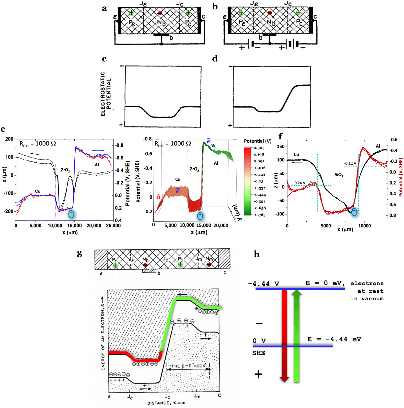 | ||
| Fig. 1 The first configurations of the W. Shockley bipolar transistor (adapted from W. Shockley, Electrons and Holes in Semiconductors, New York, D. Van Nostrand, 1950)31 in comparison with Cu/ZrO2/Al and Cu/SiO2/Al cells; (a) p–n–p double junction without applied bias; (b) p–n–p double junction with applied bias; (c) corresponds to the electrostatic potential of (a); (d) corresponds to the electrostatic potential of (b); (e) surface topography and SKP 1D and 3D surface potential of a Cu/ZrO2/Al cell in closed circuit with a 1000 Ω resistor showing apparent similarities to (c) and (d), (f) with a Cu/SiO2/Al cell at open circuit voltage OCV, and in particular in (g) showing the energy of an electron in a p–n–p–n cell; (h) standard hydrogen electrode SHE vs. absolute physical scale, where E = 0 eV, for electrons at rest in a vacuum. Note: the shape of the surface potential corresponding to (c) and (d), and the red/green curve in (g) do not depend on the semiconductor character of the materials; the surface potential depends on the relative chemical potential of the materials in electrical contact in the cell, on the insulator character (i.e., dielectric, semiconductor, electrolyte, ferroelectric, and topologic insulator), and on the density of states (DOS) of the conductors determining the capacity of bending and equalizing the potentials not only at the interface but away from it, at the edges and in pockets and “docks”. Materials like ZrO2, SiO2 ref. 32 and 33, and SnO2 ref. 32 will not allow equalization of the surface chemical potentials of Cu‖Al even in a closed circuit, with the cell corresponding to an asymmetric potential quantum well with the height related to the internal impedance, as shown in (c) and (d). | ||
As hypothesized and demonstrated previously,32,34–37 the surface potential depends much more on the chemical potential than on the type of material. It depends on the capacity of the materials to polarize, transport charges, transmit surface plasmon polaritons (SPP),38 and accommodate a wide range of potentials by bending their surface chemical potential, creating patterns; in other words, it depends on the emergent properties of the materials in heterojunctions. The surface potential is contingent upon several factors, including the relative chemical potential of the materials in electrical contact within the cell, the nature of the insulator (dielectric, semiconductor, electrolyte, ferroelectric, and topologic insulator), and the density of states DOS of the conductors. These factors are crucial in determining the capacity for bending and equalizing surface potentials at the interface and extending away from it in areas such as edges, pockets or bowls, and “docks”.
Certain materials like ZrO2, SiO2 ref. 32, 33 and 38, and SnO2 ref. 32, insulators with no unique electrical properties, exhibit limitations in equalizing their surface chemical potentials in a Cu/insulator and insulator/Al in a Cu/insulator/Al cell, or Cu/insulator and insulator/Zn in a Cu/insulator/Zn cell,32,34,37 even within a closed circuit with a resistor load. This disparity in the results for an asymmetric potential quantum well is associated with the cell's internal impedance (Fig. 1d–g). Hence, in the latter cases, independently of the electrochemical potential equalization, the equalization of the surface and chemical potentials (Fig. 1h) occurs at the interface metal1/insulator and a point away from the interface insulator/metal2 in the bulk metal2, independently of the nature of metal1 and metal2. Aluminum is especially prone to bending its surface potential and to assuming a wide range of potentials due to its DOS configuration, as shown previously.36
Hereafter, it is highlighted that the emergent character of a horizontal cell containing two dissimilar HfO2–metal heterojunctions where ferroelectricity and topologic transport are observed at room temperature in HfO2 is not expected in the single monoclinic allotrope.
Results and discussion
Hafnium dioxide exhibits several crystalline forms; the most stable is the monoclinic phase P21/c (Fig. 2a), which is stable below 1700 °C. When temperatures rise between 1700 °C and 2600 °C, hafnia transitions to the P42/nmc tetragonal phase. At temperatures exceeding 2600 °C, it converts to the Fm![[3 with combining macron]](https://www.rsc.org/images/entities/char_0033_0304.gif) m cubic phase.2,12,39 Altering the particle size to nanometer powders can stabilize different phases at room temperature. For example, reducing the particle size to approximately 10 nm can stabilize the tetragonal and cubic phases.40 The orthorhombic Pca21 phase of HfO2 is the ferroelectric phase, and it is typically stabilized in thin films by doping and strain. The ferroelectric orthorhombic phase is often stabilized during the annealing process in thin films of doped HfO2. The annealing temperatures typically range from 400 °C to 600 °C, but the exact temperature depends on the deposition method, the type of dopant (e.g., Zr, Si, Y, Al), and other processing conditions like film thickness. However, the monoclinic and the tetragonal allotropes may also become ferroelectric by recurring doping, strain, and nanosized alternatives.
m cubic phase.2,12,39 Altering the particle size to nanometer powders can stabilize different phases at room temperature. For example, reducing the particle size to approximately 10 nm can stabilize the tetragonal and cubic phases.40 The orthorhombic Pca21 phase of HfO2 is the ferroelectric phase, and it is typically stabilized in thin films by doping and strain. The ferroelectric orthorhombic phase is often stabilized during the annealing process in thin films of doped HfO2. The annealing temperatures typically range from 400 °C to 600 °C, but the exact temperature depends on the deposition method, the type of dopant (e.g., Zr, Si, Y, Al), and other processing conditions like film thickness. However, the monoclinic and the tetragonal allotropes may also become ferroelectric by recurring doping, strain, and nanosized alternatives.
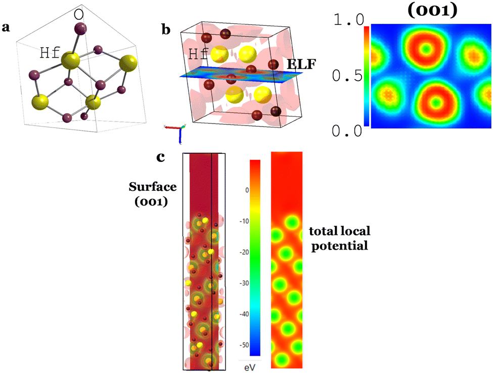 | ||
| Fig. 2 Structure of hafnium oxide (monoclinic phase P21/c); (a) crystalline structure; (b) electron localization function (ELF) of a (001) slice; ELF = 1 and ELF = ½ corresponding to the localized and electron gas; (c) total local potential of a surface (001) of HfO2. | ||
For the HfO2–ZrO2 system, other phases may show ferroelectric properties,41–43 such as the rhombohedral Hf(Zr)1+xO2 ref. 43.
The electron localization function (ELF) and the 3-dimensional (3D) and 2D total local potential of a surface (001) of HfO2 are shown in Fig. 2b and c. The electronic band structure of HfO2 (Fig. 3a) and the surface in the Brillouin zone at E = −2.5 eV near the Fermi surface in Fig. 3b show the insulator character as expected.
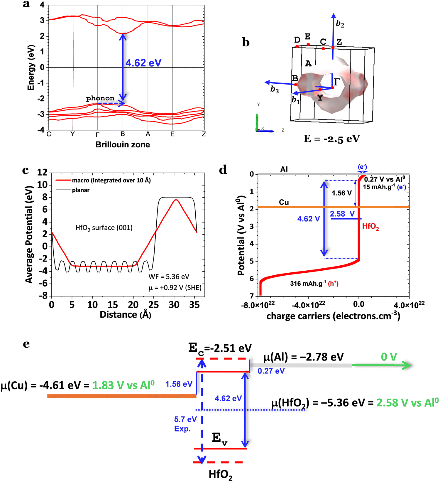 | ||
| Fig. 3 Electrical and potential energies for HfO2 (monoclinic phase P21/c). (a) The electronic band structure (indirect band gap) showing a gap energy of 4.62 eV. (b) A surface with E = −2.5 eV in the Brillouin zone, approximately the energy of the Fermi surface. (c) The total energy potential of the (001) surface in Fig. 2c where the average potential was integrated over 10 Å, showing a work function, WF = 5.36 eV corresponding to the chemical potential of μ = +0.92 V (SHE). (d) The chemical potential of HfO2versus Al0, where the Al0 chemical potential is EC(HfO2) − μ(Al0) = 0.27 V above the minimum energy of the conduction band EC(HfO2), leading to HfO2 likely being reduced by the Al to a 15 mA h g−1 maximum electronic capacity until the chemical potentials of Al and HfO2 equalize. The charge carriers in HfO2 are holes, h+. From Cu to HfO2, there are no expected substantial electronic transfers as the valence band of HfO2, as an insulator, is expected to be nearly filled at room temperature, as highlighted by the density of charge carriers being 8 × 10¹⁸ holes cm−3 at OCV, indicating a residual probability of electrons occupying the EC(HfO2). (e) 1D interpretation of (d), showing absolute chemical potentials for Cu/HfO2/Al and the conductor and valence bands energies for HfO2 for the relative positions of the cell tested by SKP. Note: if the band gap energy of HfO2 is 5.7 eV, then EC > μ(Al) (dashed line in (d)), and the reduction of HfO2 is related to a Schottky barrier of 0.27 V = EC − μ(Al) overcome upon charge. | ||
The work function was calculated from the average potential of the surface in Fig. 3c, taking into account the definition of work function: WF(HfO2) = 5.36 eV (Fig. 3c), which corresponds to the chemical potential μ = +0.92 V (SHE) where μ(SHE) = 0 V is defined as −4.44 eV in the absolute physical scale in Fig. 1h. The total average potential was simulated for a surface (001) in Fig. 2c by performing the average of the total chemical potentials integrated over 10 Å. The potential difference (V vs. Al0) versus the number of charge carriers (+ for electrons, − for holes) is shown in Fig. 3c and d.
Ferroelectric and topological insulator
HfO2 is a ferroelectric that has been substituted for SiO2 in transistors. Usually, it must be doped, for example, with Zr4+, or reduced into nano-dimensions to reveal its ferroelectric character.19 The allotrope known to be polar is the orthorhombic Pca21. Nevertheless, it is well known that the monoclinic phase (P21/c) in pure HfO2 is the most stable bulk phase under standard experimental conditions. It shows a lower dielectric constant and, therefore, a reduced ferroelectric character. However, herein, we show emergent features where the most stable HfO2 bulk phase under standard experimental conditions in a cavity Al/HfO2/Cu cell shows markedly ferroelectric properties. At μm-sizes, HfO2 has the advantage of not being hygroscopic.8,9SKP studied the most stable configuration of commercial HfO2 in a Cu/HfO2/Al cell (Fig. 4). This cell measures the species’ surface potentials, equal to the absolute chemical potentials in bulk in equilibrium (Methods eqn (8)). Not only have the ferroelectric properties been observed, but topologic conduction features have also been observed, favored by SPP propagation through the cell's surface and the ferroelectric character of HfO2.
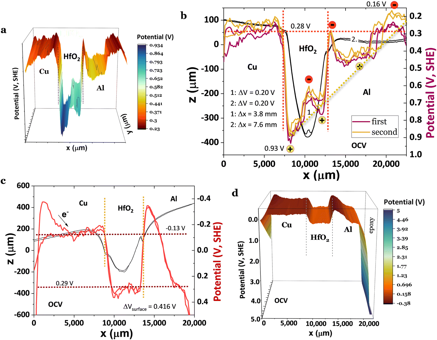 | ||
| Fig. 4 Topography and surface chemical potentials for a Cu/HfO2/Al cell showing the same surface chemical potentials for the two heterojunctions and the two electrodes away from the interfaces characteristic of a ferroelectric.32,34,37 (a) and (b) 3D surface and analysis of the surface chemical potential of the Cu/HfO2/Al at OCV showing an alignment of the surface chemical potentials of Cu/HfO2 and HfO2/Al at +0.28 V(SHE); Cu may not exchange electrons with HfO2, but Al may align diagonally in a wavy-like surface potential through positive polarization from the Cu/HfO2 interface at 7.5 mm to the cell's extremity at the Al, at 22.5 mm, an alignment through 15.0 mm corresponding to a constant electric field of 45.5 V m−1; SKP analysis shows apparent propagation of the SPP from the HfO2 to the Al, likely from the Cu to the Al through the HfO2 surface; the transmitted wave has a similar amplitude (ΔV) and doubles the wavelength (Δx) of the incident wave propagating on the surface of the oxide; it is worth noting that the electrode connected to the SKP is Cu. (c) and (d) Electron transport from the SKP to Cu leading to the equalization of the surface chemical potentials Cu/HfO2 and HfO2/Al at −0.13 V at OCV; the surface potential of HfO2 equalizes with the Al away from the interface at 0.29 V; then, the Al potential drops to 5 V(SHE) because of the interface with epoxy resin. Note: in (a) and (b), the SKP was performed with the probe-tip at 100 μm and (c) and (d) at 150 μm from the cell. The minimum potential in (b), 0.93 V(SHE), agrees with the absolute chemical potential calculated in Fig. 2c, 0.92 V(SHE). | ||
The capacity of HfO2 to polarize is clear, with two positive regions separated by a more negatively charged region (Fig. 4a and b). Notably, the Cu-side of HfO2 corresponds to the more positively charged region of HfO2, which agrees with the probability of the Al to transfer electrons (by tunneling) to HfO2 to its almost empty conduction band EC(HfO2) corresponding to a maximum capacity of 15 mA h g−1 (Fig. 3d and e). Note that if the energy of the band gap of HfO2 is 5.7 eV, then EC > μ(Al), and the reduction of HfO2 is not as likely to occur spontaneously due to the contact with Al corresponding to a Schottky barrier of 0.27 V. In Fig. 4b, the positively polarized regions are also aligned along the line with a slope of 45.5 V m−1, corresponding to a constant electric field.
Another exciting feature that corroborates the insulator character and, simultaneously, the metallic character with the transport of surface delocalized electrons in HfO2 is that the amplitude of the transmitted wave through the aluminum is approximately the same (ΔV) as in HfO2. However, the wavelength (Δx) is double that of the incident wave. The transmitted wave is shown in Fig. 4a and b. ψt(x) = Tψi(x), where ψi(x) is the incident wave, and 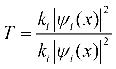 ref. 44, where kt and ki are the wavevectors of the transmitted and incident waves, respectively, with k = 2π/λ where λ = Δx (Fig. 4b). For the waves at the interface of HfO2/Al at OCV (Fig. 4b), the incident wavevector is ki,HfO2/air = 16.5 cm−1, and the transmitted wavevector is kt,Al/air = 8.3 cm−1 corresponding to f(HfO2/air) = 0.08 THz (Table 1) and f(Al/air) = 0.04 THz, which relates to the resonant frequency of molecular rotations and electrons spin flip with essential applications in quantum computing. Microwave SPPs are designated spoof surface plasmons.
 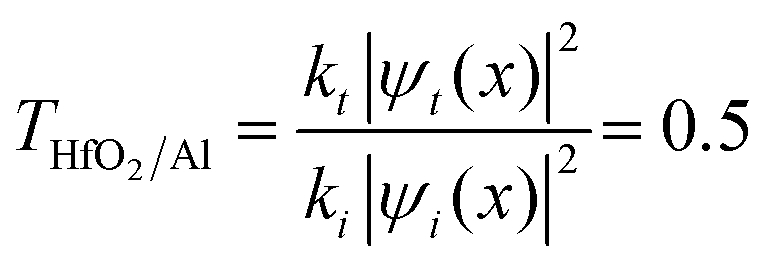 , where |ψt(x)|2 = |ψi(x)|2 = 0.04 V. This equation is fundamental in understanding wave-particle duality and the behavior of particles at barriers or interfaces. It quantifies the likelihood of a particle or wave passing through a potential barrier. The transmission coefficient for electromagnetic waves at an interface can also be calculated regarding the two materials’ electromagnetic impedances (Z1 and Z2). The transmission coefficient (T) in terms of impedances is given by
 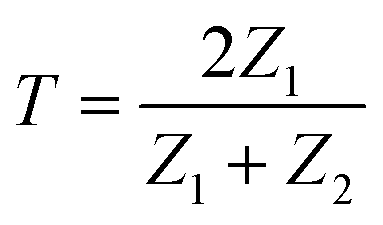 in ref. 45, where Z1 is the impedance of the incident medium (HfO2) and Z2 is the impedance of the metal (Al). The formula describes the fraction of electromagnetic energy transmitted from the HfO2 medium to Al. A relationship between the impedances of Al and HfO2 is established as follows:
  , where Al is not connected to the SKP and has no contact with Cu, thus posing a higher impedance despite being a metal. Another reason might be the fast topologic conduction in HfO2 or the impedance arising from the oxide layer Al2O3, formed on the surface of Al, hindering the Al electrode's conductive behavior and possibly contributing to a decrease in its surface potential.
| Polariton type | T (°C) | λ P (μm) | ω P/2π (THz) | Spectrum | Ref. |
|---|---|---|---|---|---|
| HfO2 metallic cavity surface-induced | 36 | 3800 | 0.08 | Far-infrared to microwave | This work (SKP, Fig. 4b) |
Fig. 4c and d show the interface Cu/HfO2 aligned with the Cu potential on the left after the transport of electrons from the SKP to the heterojunction (Cu/HfO2) and the subsequent equalization with the surface potential of the heterojunction HfO2/Al, and again with Al at −0.13 V(SHE). The surface potential of the Al aligns with the epoxy potential on the right. However, before that, the bulk surface potential of HfO2 aligns or equalizes with the Al's at 0.29 V, showing all the possible equalizations of the surface potentials of the materials along 21.9 mm. The Cu's surface potential (0.3 mm; 0.29 V) aligns with the interface of the Al/epoxy (18.4 mm; 0.29 V).
When the cell in Fig. 5 is connected to a resistor load of 980 Ω, SPP wave stripes charged alternately negative–positive are transported from the Cu through the surface of the HfO2 to the Al, as demonstrated in Fig. 5a–d, matching to solitons reported in ref. 46 and 47. The latter phenomenon will likely justify the cell's bulk potential self-charge of +0.21 V (Fig. 5d), even when the cell was connected to a resistor, 1842 Ω cmHfO2. Fig. 5a shows a reflected wave on the Al, similar to the one in Fig. 5b and c; it looks as if two different phenomena are superimposed and take place at different times: (1) the equalization of the chemical potentials Cu, Cu/HfO2, HfO2/Al, Al at a fixed value of −0.11 V (Fig. 5a and d) with waves at the interface HfO2 and a bowl shape at the Al surface; (2) the characteristic SPP with the transport of plasmons (electrons) through the surface, including the insulator HfO2 (Fig. 5b and c) inducing a magnetic field 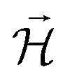 , and wave propagation through the air/metal interface characterized by
 ![[k with combining right harpoon above (vector)]](https://www.rsc.org/images/entities/i_char_006b_20d1.gif) p. Both give rise to a striped, coherent pattern. This latter phenomenon in Fig. 5c and d is the experimental materialization of the theoretical schematics in Fig. 5e. In Fig. 5c, corresponding to (2) discussed herein, the SPP is less attenuated, f(Cu/air) = 0.824 THz for a wavelength of λCu/air = 0.364 μm, and f(HfO2/air) = 0.923 THz for a wavelength of λHfO2/air = 0.325 μm (89% of λCu/air) in a Cu/HfO2/Al cell in a closed circuit with a 980 Ω resistor connected to the SKP by the Cu.
p. Both give rise to a striped, coherent pattern. This latter phenomenon in Fig. 5c and d is the experimental materialization of the theoretical schematics in Fig. 5e. In Fig. 5c, corresponding to (2) discussed herein, the SPP is less attenuated, f(Cu/air) = 0.824 THz for a wavelength of λCu/air = 0.364 μm, and f(HfO2/air) = 0.923 THz for a wavelength of λHfO2/air = 0.325 μm (89% of λCu/air) in a Cu/HfO2/Al cell in a closed circuit with a 980 Ω resistor connected to the SKP by the Cu.
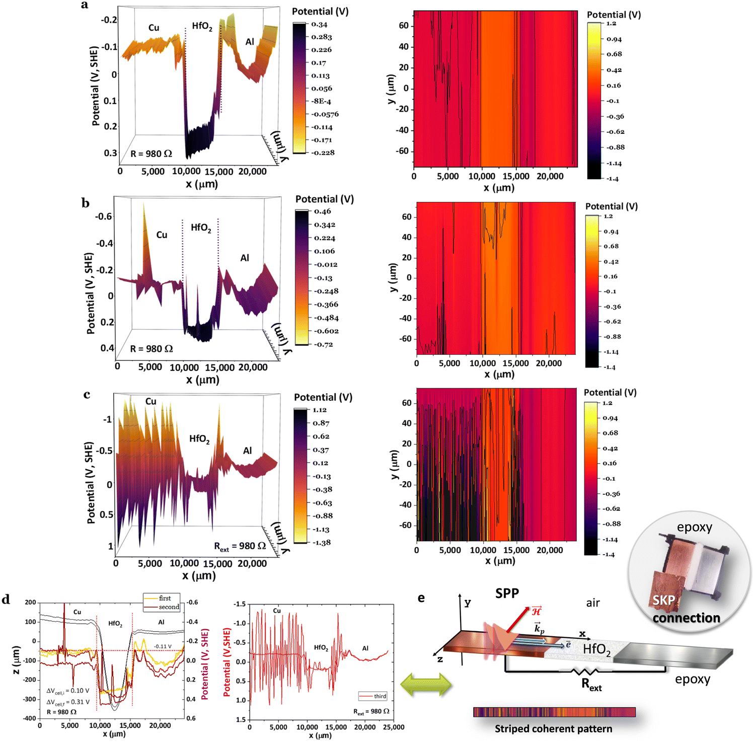 | ||
Fig. 5 Surface chemical potentials for a Cu/HfO2/Al cell in a closed circuit while connected to a resistor load of 980 Ω, showing equalization of the surface chemical potentials for both heterojunctions with HfO2; the SKP probe-tip was positioned 100 μm from the cell during the analyses; (a)–(d) three consecutive SKP analysis showing the apparent propagation of the SPP from the Cu to the Al through the HfO2 surface. After closing the circuit through a resistor load of 980 Ω, the cell shows emergent phenomena characterized by plasmonic stripes parallel to the y-axis, traveling across the x-axis, which are significant in (c);46,47 (e) unidirectional propagation of SPP48 transporting a current of electrons through Cu, and an electromagnetic wave with p through the air, inducing a magnetic field,  leading to a quasi-coherent striped pattern on the surface of the Cu and the interface HfO2/Al. Right: The image of the actual horizontal cell. Notably, in (c), negatively polarized polarons alternate with positive ones on the surface of the Cu and HfO2/Al interface. It is worth noting that even with the resistor of 980 Ω, the cell's bulk potential increases with time from 0.10 to 0.31 V, highlighting the capacity for transmitting SPP from Cu through HfO2 to Al. It is also noteworthy that Cu's surface potential fully aligns with the surface potential of the Cu/HfO2 and HfO2/Al interfaces and with the Al extreme edge (27.5 mm) at −0.11 V. leading to a quasi-coherent striped pattern on the surface of the Cu and the interface HfO2/Al. Right: The image of the actual horizontal cell. Notably, in (c), negatively polarized polarons alternate with positive ones on the surface of the Cu and HfO2/Al interface. It is worth noting that even with the resistor of 980 Ω, the cell's bulk potential increases with time from 0.10 to 0.31 V, highlighting the capacity for transmitting SPP from Cu through HfO2 to Al. It is also noteworthy that Cu's surface potential fully aligns with the surface potential of the Cu/HfO2 and HfO2/Al interfaces and with the Al extreme edge (27.5 mm) at −0.11 V. | ||
It is worth highlighting that in Fig. 5, the SKP experiments were performed with the probe tip 100 μm from the cell, with no saturation of the potential (V), and with the cell in a closed circuit with a resistor load, propitiating the connection of Cu and Al through the external circuit.
Fig. 6a shows the same trend as Fig. 5a and 6b, however, with a similar wavy phenomenon as shown in Fig. 5a and slightly higher than in Fig. 6b, likely due to the distance between the probe and the sample, which is 100, 150, and 200 μm, for Fig. 5a, 6a and b, respectively. Another possible interference on the morphology of the surface potential is the discharging time through the external resistor, as the SPP, even if not observed when the SKP probe is at higher distances, keeps being transported at the metal/air interface. However, the distance from the probe tip was purposely enlarged due to elevated saturation probability. As mentioned, the Cu/HfO2/Al surface potential cell morphology is very similar to OCV's, even upon closing the circuit with an external material resistor of 980 Ω (3920 Ω cmcell); however, in Fig. 6a, the Al surface chemical potential decreased even further to 0.12 V for x > 20 mm compared to that in Fig. 5a and 6b, aligning with the surface chemical potentials of the HfO2/Al heterojunction. With the system closed by a load, the surface chemical potential of the HfO2 increased (physical absolute scale of Fig. 1h), corresponding to a decrease in the work function of ΔWFHfO2 = −0.71 eV. This reinforces the hypothesis that surface-delocalized electrons of the ferroelectric with topologic insulator features are also transported in the circuit, leading to self-charge. The transmitted waves correspond to tunneling through a quantum square-approximate barrier.49 The behavior of HfO2 in a Cu/HfO2/Al cell is reproducible, even when fresh powders of HfO2 are introduced in the gap.
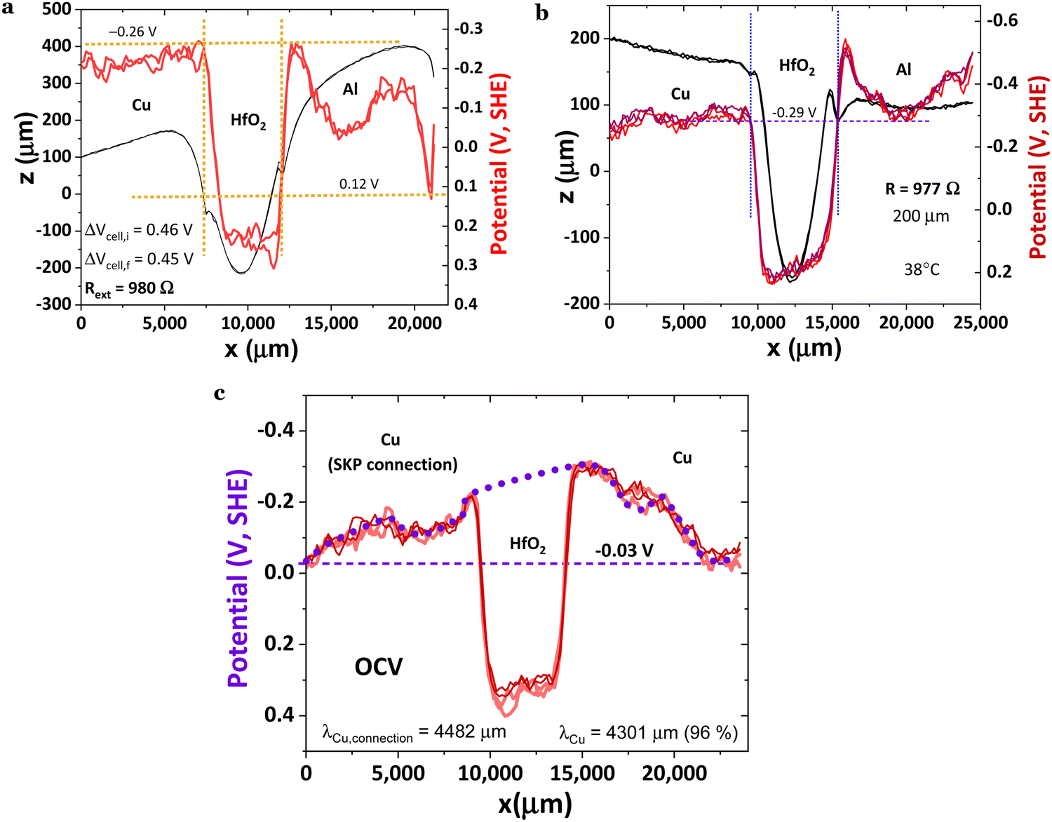 | ||
| Fig. 6 Surface chemical potentials for Cu/HfO2/Al cells in a closed circuit while connected to a resistor load of ∼980 Ω; (a) showing equalization of the surface chemical potentials for Cu/HfO2 with Al at −0.26 V and HfO2/Al with Al at 0.12 V with the SKP probe tip positioned 150 μm from the cell during the analyses; (b) showing equalization of the surface chemical potentials for Cu/HfO2 with HfO2/Al and Al with the SKP probe positioned 200 μm away from the cell during the analyses; (c) symmetric Cu/HfO2/Cu cell at OCV showing equalization of the chemical potentials at Cu (0 μm), Cu/HfO2, HfO2/Cu, and Cu (22.5 mm) at −0.03 V with the plasmonic waves incident and transmitted in both Cu(s) being not attenuated or suffering a small attenuation through the HfO2, which performs as a connection between both coppers, the first Cu connected to the SKP and the second Cu in electrical contact with the first through the HfO2. The wavelength of the plasmonic waves on the surface of the Cu connected to the SKP is λCu,connection/air = 4482 μm, and in the remaining Cu is λCu/air = 4301 μm, corresponding to 96% of the wavelength of the Cu connected to the SKP. | ||
HfO2 was also tested on a Cu/HfO2/Cu symmetric cell to finally achieve a profile shown in Fig. 6c. Even if both copper electrodes have their interface surface potentials equal to −0.03 V, they show SPP propagation with barely the same wavelength for the Cu connected to the SKP and the Cu just in contact with HfO2, corresponding to f(Cu/air) = 0.07 THz (Fig. 6c), very similar to the previously calculated HfO2 frequency f(HfO2/air) = 0.08 THz (Table 1), and f(Al/air) = 0.04 THz in a Cu/HfO2/Al cell at OCV, connected to the SKP by the Cu (Fig. 4b). The wavelength of the plasmonic waves on the surface of the Cu connected to the SKP is λCu,connection/air = 4482 μm, and in the remaining Cu, λCu/air = 4301 μm, corresponding to 96% of the wavelength of the Cu connected to the SKP.
It was also demonstrated that after the SKP measurements, the cell was still polarized at ∼25 °C, showing a current at OCV of 104 μA (VOC = 0.098 V), Fig. 7a. Calculating the impedance at OCV but not taking into account the first point, 〈i〉V=0 = C·dV/dt ⇒ C = 15.5 nF ⇒ εr = 9.3 × 10⁴ ∼ 105. From the Nyquist plot, the capacitance and relative real permittivity are much smaller, C = 6.14 pF ⇒ εr = 37, approaching the expected dielectric constant of εr = 20–30. Hence, the CV per comparison with the EIS shows that even without considering the initial polarization, the cell was polarized after the SKP analyses, conducing to a permittivity ∼2500× higher than that while depolarized by the application of the alternate current.
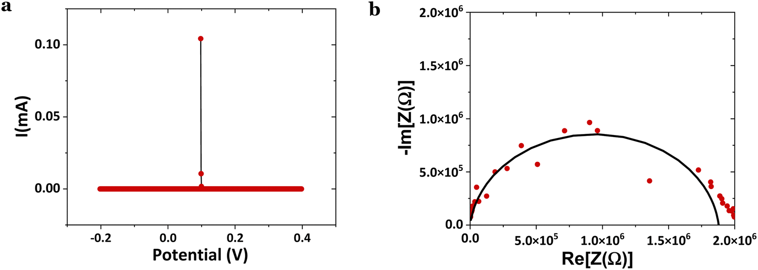 | ||
| Fig. 7 Electrochemical analyses on an Al(−)/HfO2/Cu(+) cell; (a) cyclic voltammetry CV (2 mV s−1) VOC = 0.098 V and (b) electrical impedance spectroscopy EIS performed after the experiment in Fig. 6b with measured VOC = 0.709 V. | ||
Table 2 summarizes the data for surface and bulk potentials obtained with Cu/HfO2/Al cells at OCV and with an external resistor load.
| Cell dimensions insulator: d = 5.5 mm S = 22 × 4.7 mm2 | Circuit OCV or closed with a resistance R | Heterojunction and metals at equilibria correspondent surface chemical potential | Heterojunction surface potential difference | Maximum surface potential electrode | Bulk potential difference of the cell temperature dew point, DP |
|---|---|---|---|---|---|
| Note: calculated: μCu = +0.14 V(SHE);37 experimental: μCu = +0.12 V(SHE); calculated: μAl = +0.2537 to +0.63 V(SHE); experimental: μAl = −1.01 V(SHE) and tabulated: μAl = −1.66 V(SHE).50 The Al possesses an almost invariant DOS36vs. chemical potential, which might justify its ability to shape its surface potential to a wide range of materials. | |||||
| Ferroelectric: HfO2 [polarization: positive–negative–positive] Fig. 4 | |||||
| Calculated surface chemical potential (ab initio), μ = +0.92 V(SHE) Fig. 3c; experimental: μ = +0.93 to +0.76 V(SHE) Fig. 4a and b | |||||
| Cu/HfO2/Al | OCV | Cu1…Cu2/HfO2/Al1⋯Al2 | ∼0 V | ∼0 V | 36 °C |
| Fig. 4a and b | 0.28 V | DP: <10 °C | |||
| Cu/HfO2/Al | 980 Ω | Cu1⋯Cu2/HfO2⋯Al1⋯Al2 | 0.28 V | 0.28 V | V i = 0.10 V |
| Fig. 5b and d (left) | −0.11 V | V f = 0.31 V | |||
| Cu/HfO2/Al | 980 Ω | Cu1⋯Cu2/HfO2⋯Al1⋯Al2 | 36 °C | ||
| Fig. 5c and d (right) | 0.25 V | DP: <10 °C | |||
| Cu/HfO2/Al | V i = 0.35 V, OCV | ||||
| 0.38 V | 0.38 V | V f = 0.44 V, OCV | |||
| 980 Ω | Cu1⋯Cu2/HfO2⋯Al | V i = 0.46 V, 980 Ω | |||
| Fig. 6a | −0.26 V | V f = 0.45 V, 980 Ω | |||
| 36 °C | |||||
| DP: <10 °C | |||||
Conclusions
Hafnia in a Cu/HfO2/Al cell shows the essential features of ferroelectric materials as indicated by the authors for Li2.99Ba0.005ClO, a ferroionic and ferroelectric glass electrolyte,34 namely, the ability to equalize its surface potential with two dissimilar metals, Cu and Al, with cathode and anode features, respectively.Another remarkable feature of ferroelectric materials observed herein with HfO2 (≤44 μm diameter powders) is their capacity to self-charge; a potential difference of 0.21 V through SPP transport within a Cu/HfO2/Al cell with an HfO2 thickness of 5.5 mm, corresponding to 38 V m−1 and remaining polarized after SKP analyses for subsequent I–V tests (cyclic voltammetry).
A Cu/HfO2/Al cell may propagate SPP through the Cu/air, Cu/HfO2 (edge), HfO2/air, and HfO2/Al (edge): (1) plasmons through Cu and HfO2 surfaces, and (2) polariton waves through Cu/air and HfO2/air matching the theoretical behavior of SPP with positive alternating with negative amplitude higher frequency soliton spikes and superimposing the equilibria previously achieved through contact of the cross sections or bulk interfaces (Cu/HfO2 and HfO2/Al).
At a steady state, the SPP polarization may increase the bulk dielectric constant by more than three orders of magnitude from εr ∼ 37 to ∼105 while sourcing an external resistor of ∼1 kΩ (3920 Ω cmcell). The surface chemical potential of the bulk HfO2 at OCV is +0.93 V(SHE) and matches 99% of the simulated chemical potential of +0.92 V(SHE).
Another feature that is replicated in all measurements with HfO2/Al is the capacity of aluminum, which is not connected to the SKP, to bend and form a “bowl”-like surface chemical potential (at OCV and connected to a ∼1 kΩ resistor in a closed circuit) with a more positively charged concave region and more negatively charged edges that equalize with the surface chemical potentials of the Cu and HfO2 allowing for the alignment of the surface potentials of Cu, HfO2, and Al at the interfaces and/or at the inner surface of the electrodes, in the 2D air-exposed surface Cu/HfO2/Al. However, it is also noteworthy that while Cu and HfO2 may propagate SPP with high frequency throughout the latter horizontal surface, Al may not, with these waves attenuating at the HfO2/Al edge.
With a material that behaves strictly as an insulator, such as ZrO2, the interfacial impedances are proportional to the quantum well's asymmetric heights. Even when the circuit is closed with a resistor load (discharging mode), there is a difference between the surface chemical potentials of Cu and Al at the interface with ZrO2. This feature was always observed for other electrodes when the insulators were dielectric, semiconductors, or solid electrolytes with no distinct features such as ferroelectric behavior. In contrast, the alignment between one of the two interfaces and the remaining conductor electrode (e.g., Cu/ZrO2 and Al) will still occur but at a distance from the interface in the 2D exposed electrode, which depends on the interface impedance. As higher the impedance is, the furthest away from the interface the equalization of the surface potentials will occur, and therefore, the equalization of the chemical potentials.
The unbiased p–n–p bipolar transistor only aligns the surface chemical potentials of the two p-type semiconductors if they are similar or have similar chemical potentials, such as in a symmetric cell.
In conclusion, surface potentials are characterized by a material's capacity to create polarization patterns along the surfaces, allowing them to align their bulk electrochemical and surface chemical potentials with other materials. In this topologic polarization, electrons also play an essential role, even in HfO2.
Tailoring all-solid-state transistors to fast switching involves sorting the properties of the materials while in contact with other materials, which are translated by their relative chemical potentials and capacity to equalize their surface chemical potentials.
Methods
Materials
Hafnium(IV) oxide 99% (metal basis excluding Zr) with Zr < 1.5% from Thermo Scientific with a −325-mesh screen (≤44 μm diameter) was used as purchased in a Cu/HfO2/Al or Cu/HfO2/Cu cell.Cell preparation
Before initiating the calibration steps for SKP, cell preparation is essential, which involves several steps: (1) sanding and polishing the electrodes, (2) ensuring thorough removal of particle residues, and (3) completely drying the cell. Following this preparation, the gap between the electrodes is filled with HfO2, compacted tightly using a spatula-like instrument, and leveled by the electrodes. It is important to note that the oxide should be adequately dried before proceeding with this final step.Scanning Kelvin probe (SKP)
SKP is a non-invasive and non-contact technique relying on the electrical contact potential difference (CPD) between two electrically connected metals.32,51 It utilizes a vibrating capacitor tip to measure the local work function difference between the sample and the tip, which is linked to the surface chemical potential. This enables electrochemical studies of the materials’ surfaces. SKP was employed to map surface topography using capacitive tracking measurement (CTM), and is particularly suitable for non-flat surfaces and irregularities since it maintains a constant distance between the probe tip and the sample, scanning the surface without losing crucial information.These techniques fall under the atomic force microscopy (AFM) set of methods. All SKP measurements were conducted using a Biologic SKP-M470 with SKP tips U-SKP-370/1 and U-SKP-150, made of tungsten wire with 500 and 150 μm diameter ‘SKP probes’, respectively. The distance between the CTM or SKP probe tip and the sample ranged from 100 to 200 μm, with the analysis monitored via a micro-camera. All experiments were carried out within a dry box. Notably, fresh materials were utilized after cleaning and drying the cell for each set of experiments involving each insulator (ZrO2 and HfO2-several measurements), ensuring consistency and reliability.
Electrochemical impedance spectroscopy (EIS) and cyclic voltammetry (CV)
In electrochemical impedance spectroscopy (EIS), a GAMRY impedance meter (GAMRY1000) applies a small amplitude AC signal to the cell's terminals. By analyzing the sample cell's AC voltage and current responses, impedance characteristics (resistive, capacitive, and inductive) and equivalent circuits related to their components can be determined at controlled frequencies. EIS studies are complementary to understanding surface phenomena within the cells. The frequency range for EIS was set from 1 MHz to 0.1 Hz, with an amplitude signal of 10 mV.Cyclic voltammetry, or I–V, is an electrochemical technique used to gain insights into the dynamic behavior of cells during cycles under a specified voltage rate. In the case of the present cells, I–V measurements were conducted within a potential window ranging from −0.35 to +1.0 V, employing a scan rate of 2 mV s−1.
Ab initio simulations
Ab initio simulations were conducted utilizing density functional theory (DFT) coupled with the generalized gradient approximation (GGA) pseudopotential method. These simulations aimed at determining parameters such as lattice constant, lattice stability, density, surfaces, electronic band structures, Fermi surfaces, electron localization functions, thermal conductivity, chemical potential versus charge carriers, and work functions at different temperatures. Similar to our prior research on ZnO,37 dielectrics and electrolytes,34 and SiO2, SiO, and SnO232 crystal representations without defects like vacancies and impurities were utilized in these simulations. The DFT and hybrid functional HSE06 packages, as implemented by VASP6 (Vienna Ab initio Simulation Package),52 were employed with specific parameters including a plane-wave cutoff of >400 eV, reciprocal space projection, and a spacing of k points of 0.2–0.3 Å−1.Macroscopic average potentials were simulated within a radius of 10 Å. The determination of work functions involved calculating the difference between the maximum potential where electrons are at rest on the surface and the average potential between the minimum and maximum potentials immediately before and after the line marking the surface, corresponding to the Fermi level.
Thermodynamic considerations
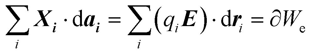
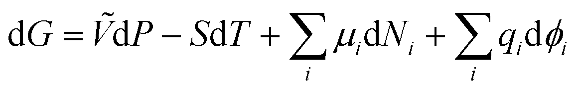
From the first law of thermodynamics dU = δQ − ∂W, where +dU is the internal energy gain by the system, +δQ is the heat gain by the system, +∂W is the work made by the exterior over the system, T is the absolute temperature, S is entropy, P is pressure, Ṽ is volume, μi is the chemical potential of species i, Ni is the number of mobile particles such as charge carriers, Xi is an intensive property such as electrical coulombic force, dai is an extensive property such as the displacement of a charge under the influence of the coulombic force dri, We electrical work, G Gibbs free energy, H enthalpy, qi = zieNi mobile charge, zi the valence of the mobile species and e the elementary charge (1.6 × 10⁻¹⁹ C), ϕ = E·dri the surface (chemical) potential exerted on the surface of species i, either due to surface effects on i or to electrical contact with other species j, and![[small mu, Greek, macron]](https://www.rsc.org/images/entities/i_char_e0cd.gif) i is the electrochemical potential. If there are mobile particles in the system of species i, such as charge carriers able to compensate for the work made on its surface,
i is the electrochemical potential. If there are mobile particles in the system of species i, such as charge carriers able to compensate for the work made on its surface,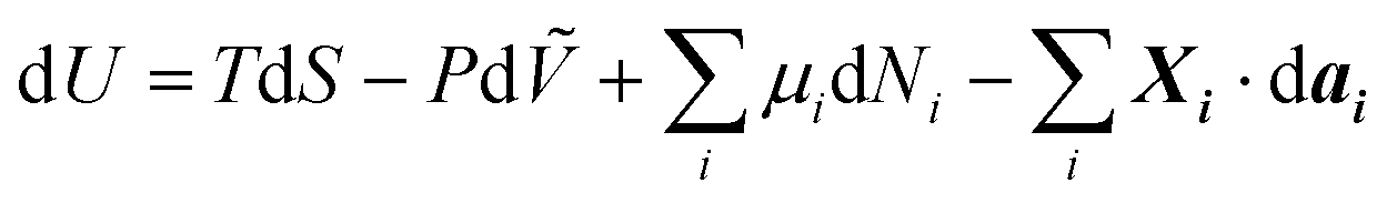 | (1) |
 | (2) |
| G = H − TS | (3) |
| H = U + PṼ | (4) |
From (3) and (4),
| dG = dU + PdṼ + ṼdP − TdS − SdT | (5) |
From (1) and (5),
 | (6) |
If P and T are constant,
 | (7) |
| i − j = μi − μj + zie(ϕi − ϕj) | (8) |
i − j = 0 = μi − μj + zie(ϕi − ϕj) where ΔVij = ϕi − ϕj. If the surface chemical potentials align (or equalized), as discussed hereafter ϕi − ϕj = 0 ⇒ μi − μj = −zie(ϕi − ϕj) = 0 then the chemical potentials equalize. If one of the species i or j is an insulator, with sufficient surface states >∼1012 cm−2 ref. 53, or containing mobile ions, a double-layer capacitor EDLC is going to form at the interface between them, corresponding to ΔVij = ϕi − ϕj as the insulator cannot be easily reduced/oxidized. The EDLC allows for the equilibration of the electrochemical potentials, storing the energy in devices such as batteries and capacitors.
Author contributions
Cell fabrication and SKP, EIS, and CV experiments: ANG. The conceptualization, formal analysis, simulations, original draft, and supervision: MHB. Both authors have read and agreed to the published version of the manuscript.Data availability
The data supporting this study's findings are available from the corresponding author upon reasonable request.Conflicts of interest
The authors declare no conflicting interests.Acknowledgements
This work was supported by the Portuguese Foundation for Science and Technology FCT UIDP/50022/2020 Emerging Technologies–LAETA. This work benefited from Agenda CVB – Cadeia de Valor das Baterias em Portugal, no. C644864613-00000003, financed by the Recovery and Resilience Plan (PRR) and by European Union and of Agenda NGS – New Generation Storage, no. C644936001-00000045, investment project no. 58, financed by the Recovery and Resilience Plan (PRR) and by European Union – NextGeneration EU.References
- A. N. Guerreiro, I. B. Costa, A. B. Vale and M. H. Braga, Int. J. Mol. Sci., 2023, 24, 15985 CrossRef CAS.
- U. Schroeder, C. S. Hwang and H. Funakubo, Ferroelectricity in doped hafnium oxide: Materials, properties and devices, Elsevier, 2019 Search PubMed.
- S. S. Cheema, N. Shanker, C. H. Hsu, A. Datar, J. Bae, D. Kwon and S. Salahuddin, Adv. Electron. Mater., 2022, 8, 2100499 CrossRef CAS.
- S. S. Cheema, N. Shanker, S. L. Hsu, J. Schaadt, N. M. Ellis, M. Cook, R. Rastogi, R. C. N. Pilawa-Podgurski, J. Ciston, M. Mohamed and S. Salahuddin, Nature, 2024, 629(8013), 803–809 CrossRef CAS PubMed.
- L. Zhang, M. Liu, W. Ren, Z. Zhou, G. Dong, Y. Zhang, B. Peng, X. Hao, C. Wang, Z. De Jiang, W. Jing and Z. G. Ye, RSC Adv., 2017, 7, 8388–8393 RSC.
- P. Zukowski, T. N. Koltunowicz, K. Czarnacka, A. K. Fedotov and I. E. Tyschenko, J. Alloys Compd., 2020, 846, 156482 CrossRef CAS.
- S. S. L. Vendra, N. Antony, E. Koroleva, A. Filimonov, S. Vakhrushev and R. Kumar, Ceram. Int., 2022, 48, 13063–13070 CrossRef CAS.
- Y. Zhao, Materials, 2012, 5, 1413–1438 CrossRef CAS.
- L. Soriano, M. Abbate, J. C. Fuggle, M. A. Jiménez, J. M. Sanz, C. Mythen and H. A. Padmore, Solid State Commun., 1993, 87, 699–703 CrossRef CAS.
- J. L. Collins, H. Moncada Hernandez, S. Habibi, C. E. Kendrick, Z. Wang, N. Bihari, P. L. Bergstrom and A. R. Minerick, Thin Solid Films, 2018, 662, 60–69 CrossRef CAS.
- R. Stoklas, D. Gregušová, S. Hasenöhrl, E. Brytavskyi, M. Ťapajna, K. Fröhlich, S. Haščík, M. Gregor and J. Kuzmík, Appl. Surf. Sci., 2018, 461, 255–259 CrossRef CAS.
- C. V. Ramana, M. Vargas, G. A. Lopez, M. Noor-A-Alam, M. J. Hernandez and E. J. Rubio, Ceram. Int., 2015, 41, 6187–6193 CrossRef CAS.
- C. Wang, D. Zhang, H. Wang, Y. Yu, Y. Li and Q. Li, J. Am. Ceram. Soc., 2015, 98, 3918–3924 CrossRef CAS.
- G. He, L. Q. Zhu, M. Liu, Q. Fang and L. D. Zhang, Appl. Surf. Sci., 2007, 253, 3413–3418 CrossRef CAS.
- D. L. Wood, K. Nassau, T. Y. Kometani and D. L. Nash, Appl. Opt., 1990, 29, 604 CrossRef CAS PubMed.
- W. Banerjee, A. Kashir and S. Kamba, Small, 2022, 18 Search PubMed.
- S. S. Cheema, N. Shanker, L. C. Wang, C. H. Hsu, S. L. Hsu, Y. H. Liao, M. San Jose, J. Gomez, W. Chakraborty, W. Li, J. H. Bae, S. K. Volkman, D. Kwon, Y. Rho, G. Pinelli, R. Rastogi, D. Pipitone, C. Stull, M. Cook, B. Tyrrell, V. A. Stoica, Z. Zhang, J. W. Freeland, C. J. Tassone, A. Mehta, G. Saheli, D. Thompson, D. I. Suh, W. T. Koo, K. J. Nam, D. J. Jung, W. Bin Song, C. H. Lin, S. Nam, J. Heo, N. Parihar, C. P. Grigoropoulos, P. Shafer, P. Fay, R. Ramesh, S. Mahapatra, J. Ciston, S. Datta, M. Mohamed, C. Hu and S. Salahuddin, Nature, 2022, 604, 65–71 CrossRef CAS.
- R. Cai, I. Weisbord, S. Caspi, L. Naamat, L. Kornblum, A. G. Dana and T. Segal-Peretz, Chem. Mater., 2024, 36, 1591–1601 CrossRef CAS.
- J. P. B. Silva, R. Alcala, U. E. Avci, N. Barrett, L. Bégon-Lours, M. Borg, S. Byun, S. C. Chang, S. W. Cheong, D. H. Choe, J. Coignus, V. Deshpande, A. Dimoulas, C. Dubourdieu, I. Fina, H. Funakubo, L. Grenouillet, A. Gruverman, J. Heo, M. Hoffmann, H. A. Hsain, F. T. Huang, C. S. Hwang, J. Íñiguez, J. L. Jones, I. V. Karpov, A. Kersch, T. Kwon, S. Lancaster, M. Lederer, Y. Lee, P. D. Lomenzo, L. W. Martin, S. Martin, S. Migita, T. Mikolajick, B. Noheda, M. H. Park, K. M. Rabe, S. Salahuddin, F. Sánchez, K. Seidel, T. Shimizu, T. Shiraishi, S. Slesazeck, A. Toriumi, H. Uchida, B. Vilquin, X. Xu, K. H. Ye and U. Schroeder, APL Mater., 2023, 11, 089201 CrossRef CAS.
- A. G. Khairnar and A. M. Mahajan, Solid State Sci., 2013, 15, 24–28 CrossRef CAS.
- X. Chi, X. Lan, C. Lu, H. Hong, C. Li, S. Chen, H. Lai, W. Huang and J. Xu, Mater. Res. Express, 2016, 3, 035012 CrossRef.
- M. Aldrigo, M. Dragoman, S. Iordanescu, F. Nastase and S. Vulpe, Nanomaterials, 2020, 10, 1–12 CrossRef.
- U. B. V. Bang, S. S. V. Anantha and P. B. Agarwal, Mater. Lett., 2022, 317, 132097 CrossRef.
- A. K. Yadav, K. X. Nguyen, Z. Hong, P. García-Fernández, P. Aguado-Puente, C. T. Nelson, S. Das, B. Prasad, D. Kwon, S. Cheema, A. I. Khan, C. Hu, J. Íñiguez, J. Junquera, L. Q. Chen, D. A. Muller, R. Ramesh and S. Salahuddin, Nature, 2019, 565(7740), 468–471 CrossRef CAS PubMed.
- O. Hemmatyar, S. Abdollahramezani, Y. Kiarashinejad, M. Zandehshahvar and A. Adibi, Nanoscale, 2019, 11, 21266–21274 RSC.
- M. Sun, M. Jiang, H. Huang, B. Yang, Y. Lin and P. Wang, Coatings, 2023, 13(5), 967 CrossRef CAS.
- R. Renaudot, V. Agache, Y. Fouillet, M. Kumemura, L. Jalabert, D. Collard and H. Fujita, Microfluid. Nanofluid., 2013, 15, 297–307 CrossRef CAS.
- S. Habibi, H. Y. Lee, H. Moncada-Hernandez and A. R. Minerick, Electrophoresis, 2022, 43, 1322–1336 CrossRef CAS PubMed.
- K. Jeong, H. Park, J. Chae, K. I. Sim, W. J. Yang, J. H. Kim, S. B. Hong, J. H. Kim and M. H. Cho, ACS Appl. Mater. Interfaces, 2020, 12, 12215–12226 CrossRef CAS.
- A. R. Jayakrishnan, J. S. Kim, M. Hellenbrand, L. S. Marques, J. L. MacManus-Driscoll and J. P. B. Silva, Mater. Horiz., 2024, 11, 2355–2371 RSC.
- Electrons And Holes In Semiconductors: William Shockley: Internet Archive, https://archive.org/details/ElectronsAndHolesInSemiconductors, (accessed 22 September 2024).
- A. N. Guerreiro, I. B. Costa, A. B. Vale and M. H. Braga, Int. J. Mol. Sci., 2023, 24, 15985 CrossRef CAS PubMed.
- R. Fang, Z. Bai, X. Wu, Q. Fan, B. Bao, C. Hou, Q. Zhang, Y. Li, K. Li and H. Wang, Adv. Opt. Mater., 2024, 12, 2400498 CrossRef CAS.
- A. N. Guerreiro, B. A. Maia, H. Khalifa, M. C. Baptista and M. H. Braga, Batteries, 2022, 8, 232 CrossRef CAS.
- B. M. Gomes, J. F. Ribeiro Moutinho and M. H. Braga, J. Mater. Chem. A, 2024, 12, 690–722 RSC.
- B. A. Maia, B. M. Gomes, A. N. Guerreiro, R. M. Santos and M. H. Braga, JPhys Mater., 2024, 7, 025001 CrossRef CAS.
- A. N. Guerreiro, M. C. Baptista, B. A. Maia and M. H. Braga, ACS Appl. Energy Mater., 2022, 5, 9811–9822 CrossRef CAS.
- M. Sich, D. V. Skryabin and D. N. Krizhanovskii, C. R. Phys., 2016, 17, 908–919 CrossRef CAS.
- S. Ferrari, M. Modreanu, G. Scarel and M. Fanciulli, Thin Solid Films, 2004, vol. 450, pp. 124–127 Search PubMed.
- C. H. Lu, J. M. Raitano, S. Khalid, L. Zhang and S. W. Chan, J. Appl. Phys., 2008, 103, 124303 CrossRef.
- A. El Boutaybi, T. Maroutian, L. Largeau, S. Matzen and P. Lecoeur, Phys. Rev. Mater., 2022, 6, 074406 CrossRef CAS.
- J. P. B. Silva, R. F. Negrea, M. C. Istrate, S. Dutta, H. Aramberri, J. Íñiguez, F. G. Figueiras, C. Ghica, K. C. Sekhar and A. L. Kholkin, ACS Appl. Mater. Interfaces, 2021, 13, 51383–51392 CrossRef CAS.
- Y. Wang, L. Tao, R. Guzman, Q. Luo, W. Zhou, Y. Yang, Y. Wei, Y. Liu, P. Jiang, Y. Chen, S. Lv, Y. Ding, W. Wei, T. Gong, Y. Wang, Q. Liu, S. Du and M. Liu, Science, 2023, 381, 558–563 CrossRef CAS.
- R. Jancel, in Foundations of Classical and Quantum Statistical Mechanics, ed. D. ter Haar, Elsevier, 1963 Search PubMed.
- S. A. Maier, Plasmonics: Fundamentals and applications, Springer, US, 2007 Search PubMed.
- Y. M. Shnir, Symmetry, 2021, 13, 1–22 CrossRef.
- Y. Ye, L. Bu, W. Wang, S. Chen, F. Baronio and D. Mihalache, Front. Phys., 2020, 8, 596950 CrossRef.
- K. Y. Bliokh, F. J. Rodríguez-Fortuño, A. Y. Bekshaev, Y. S. Kivshar and F. Nori, Opt. Lett., 2018, 43, 963 CrossRef CAS PubMed.
- H. G. Winful, Phys. Rev. Lett., 2003, 91, 260401 CrossRef.
- S. Trasa’tti, Pure Appl. Chem., 1986, 58, 955–966 CrossRef.
- X. Zhu, R. I. Revilla and A. Hubin, J. Phys. Chem. C, 2018, 122, 28556–28563 CrossRef CAS.
- G. Kresse and J. Furthmüller, Phys. Rev. B: Condens. Matter Mater. Phys., 1996, 54, 11169–11186 CrossRef CAS PubMed.
- J. Bardeen, Phys. Rev., 1947, 71, 717 CrossRef.
| This journal is © The Royal Society of Chemistry 2024 |