
 Open Access Article
 This Open Access Article is licensed under a Creative Commons Attribution-Non Commercial 3.0 Unported Licence
Grain boundary effect unveiled in monolayer MoS2 for photonic neuromorphic applications†
Navaneeth
Krishnan K
 ,
Sandaap
Sathyanarayana
and
Bikas C.
Das
*
,
Sandaap
Sathyanarayana
and
Bikas C.
Das
*
eNDR Laboratory, School of Physics, IISER Thiruvananthapuram, Trivandrum 695551, Kerala, India. E-mail: bikas@iisertvm.ac.in
First published on 20th August 2024
Abstract
Layered 2D materials with grain boundaries (GBs) hold promise for various applications. Despite considerable progress, deliberately introducing GBs remains a challenge during 2D material growth. In this study, we explored the significance of GBs in monolayer molybdenum disulfide (ML MoS2) in optoelectronic functionalities such as photodetection, photonic synaptic behaviours, and adaptive learning analogous to the brain. Our comparative analysis revealed that GB-free MoS2 devices demonstrated a superior photodetector performance, featuring a remarkably high dark-to-light current ratio of 105 at −1.0 V, with responsivity reaching 10 A W−1, detectivity soaring to 1015 W−1, and a noise equivalent power of about 10−16 W √Hz−1, outperforming devices containing GBs. Moreover, GBs significantly delayed the response speed, indicating the prevalence of persistent photoconductance. Conversely, GBs facilitated the replication of various optoelectronic synaptic behaviors and adaptive learning of the brain. Our experimental results uncovered the sharp and robust atomic stitching of MoS2 domains at GBs, which act as charge carrier recombination centers due to the presence of defects. Notably, GBs induced a barrier within the energy bands by shrinking the bandgap, hindering the flow of photogenerated carriers. We systematically elucidated this phenomenon through energy band diagrams and electrostatic force microscopy results from biased samples under illumination.
1. Introduction
The field of neuromorphic computing has seen significant progress, with ongoing research and development efforts aimed at creating novel devices and architectures using different advanced and smart materials.1–4 In traditional computing, information is processed using a central processing unit (CPU) based on the von Neumann architecture, which separates memory and processing units.5 Neuromorphic computing conversely aims to mimic the parallel processing and learning capabilities observed in the brain. Devices for neuromorphic computing are classified into various types based on criteria such as their architecture, operation principles, materials used, and application areas.6–8 Accordingly, a photonic memristor or optoelectronic neuromorphic device is a type of device that combines the principles of neuromorphic functionalities and optoelectronics using light (photons), which is quite complex to design.9,10 They offer low-power memory storage and computation, paving the way for more efficient artificial intelligence systems and next-generation optical communication technologies.11 Interestingly, two-dimensional transition metal dichalcogenides (2D TMDCs), such as molybdenum disulfide (MoS2), rhenium disulphide (ReS2), and tungsten disulphide (WS2), play a significant role in the design of photonic neuromorphic devices due to their high absorption coefficient, ultrafast carrier dynamics, and non-linear optical properties.7,12 Photonic neuromorphic devices leverage the unique properties of 2D TMDCs to achieve efficient light–matter interaction and mimic certain aspects of neural processing similar to that in our brain.3,10,13Since the discovery of graphene in 2004 using scotch-tape exfoliation, a similar strategy was adopted to isolate the monolayer from the bulk crystal of TMDCs to open up a new realm of possibilities.14 Later, techniques such as liquid-phase exfoliation, redox exfoliation, hydrothermal growth, and chemical vapour deposition (CVD) were adopted to grow the monolayer to a few layers of 2D TMDCs.15–17 Because of scalability and quality, the CVD technique has been used to grow high-quality large-area 2D TMDCs on different substrates, including Si/SiO2 and quartz. In general, CVD-grown 2D TMDCs depict the polycrystalline nature of the assembly of multiple domains, which are stitched by the well-defined grain boundaries (GBs) originating from the presence of defects such as dislocations, vacancies, and dangling bonds.18,19 GBs in 2D layered materials significantly affect the electronic and optical properties as the centres of carrier scattering and recombination. The effect of GBs on 2D layered material devices remains a long-lasting topic of interest in materials science and nanotechnology to demonstrate exciting applications.20 Previously, 2D TMDCs have been investigated for developing devices, such as transistors, photodetectors, sensors, memristors, and catalytic electrodes, but the GB effect is mostly ignored. The lack of knowledge of the GB effect in 2D layered TMDCs limits many potential applications, including the merging of optoelectronics and neuromorphic computing.21,22
In this study, we grow 2D monolayer (ML) MoS2 of different shapes using the CVD technique at a relatively lower temperature, and sodium chloride (NaCl) is used as the seeding promoter. Systematic characterizations reveal that the MoS2 flakes of a triangular shape are single crystalline. However, the shapes of four and six-point stars of MoS2 contain sharp GBs, which are further characterized to reveal the elemental composition, scattering nature, optical emission, and structural properties of MoS2 GBs step-by-step.23 To reveal the effect of GBs on the optoelectronic property, a planar device of metal/semiconductor/metal (MSM) structure was fabricated using MoS2 samples of triangular and six-point star shapes. Then, current–voltage characteristics, both the DC sweep and temporal, were recorded under dark and light of varying intensities for both devices, and various photodetector performance parameters were estimated, including responsivity (R), detectivity (D), signal-to-noise ratio (SNR), and noise equivalent power (NEP). An advanced AFM mode, such as electrostatic force microscopy (EFM), is used to visualize the role of GBs precisely. Interestingly, the MSM device of ML MoS2 with GBs shows various optoelectronic synaptic actions and adaptive learning behaviour of the brain.
2. Results and discussion
2.1. Growth and characterization of MoS2 and GB-mediated MoS2
To probe the property of the grain boundary (GB) present in monolayer molybdenum disulphide (ML MoS2) and how it modulates the optoelectronic device functionality and related applications, a controlled growth process is crucial for intentionally incorporating GBs into the samples. For that, we utilize a slightly modified chemical vapour deposition (CVD) technique, as reported elsewhere, at a relatively lower growth temperature (600 °C) in the presence of NaCl seeding promoter.17,23,24 Accordingly, we successfully demonstrated a recipe for growing monolayer MoS2 samples of different shapes on the Si/SiO2 substrates based on the strategy of locating substrates inside the growth chamber relative to the seeding promoter NaCl and Mo-precursor, as illustrated in Fig. S1 in the ESI.†Fig. 1(a–c) depicts the recorded optical microscope (OM) images of the CVD-grown ML MoS2 samples of shapes, such as triangular, four-point star, and six-point star, respectively. These OM images appear almost uniform in contrast and might be monocrystalline. However, a different nature is discovered after recording the SEM images due to the appearance of GB. Particularly, the triangular MoS2 flake appears GB-free (Fig. 1d), and the other two samples contain sharp GB stitched between domains (Fig. 1e and f). It would be intriguing to investigate further the origin of GB in these CVD-grown ML MoS2 samples and reveal the possible mechanism of shape evaluation systematically. Eventually, we recorded the photoluminescence (PL) mapping images of the above samples, as shown in Fig. 1(g–i), and found an interesting correlation between the GBs and bright PL spots. Despite having bright PL regions at the edges of the triangular ML MoS2 sample (Fig. 1g), the GBs are also bright in the PL mapping images of the four-point and six-point star samples, as depicted in Fig. 1h and i, respectively. Usually, the edges are vacancy-dominated in terms of missing atoms, dangling bonds, and defects in the crystal lattice structure, which were found more efficient to emit the absorbed photons by serving as radiative recombination centers for the photogenerated charge carriers, which are further modulated by the intrinsic strain existing at the GBs.23 The monolayer thickness of these MoS2 samples is strongly supported by the recorded AFM topography images, and the thickness is found to be mostly about 1 nm, as shown in Fig. S2 in the ESI.†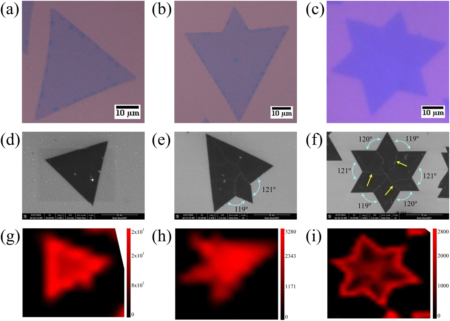 | ||
| Fig. 1 (a)–(c) Optical microscope image of the grown MoS2 samples starting from the three-point star to the six-point star. (d)–(f) Scanning electron microscope image of the grown MoS2 samples. (g)–(i) Photoluminescence (PL) mapping of MoS2 samples recorded by exciting with a light wavelength of 532 nm. | ||
The growth conditions, including temperature, pressure, and precursor flow rates, play a crucial role in determining the final shape and size of the MoS2 flakes in the CVD process. In this technique, molybdenum and sulfur precursors are vaporized and transported to a prepared substrate in the presence of a NaCl seeding promoter. Typically, MoS2 nucleates first on the substrate, forming islands that grow through the addition of more molybdenum and sulfur atoms. The mechanism behind this shape evolution is strongly influenced by the molybdenum![[thin space (1/6-em)]](https://www.rsc.org/images/entities/char_2009.gif) :sulfur (Mo:S) precursor ratio, along with the growth rate of different faces of the nucleated sites.23 Generally, the faces that grow quickly either shrink or vanish completely, while the slower faces eventually grow to larger dimensions. Moreover, the growth rate is determined by the surface free energy, which is higher at a slower rate. In our experiment, the Si/SiO2 substrate positioned closest to the NaCl catalyst exhibited the highest coverage of MoS2 flakes with a six-point star shape featuring 12 vertices. As the distance increases, the density of flakes decreases, accompanied by a reduction in the number of vertices in the shapes, as depicted by the recorded optical images of the three substrates in Fig. S1 in the ESI.† NaCl acts as a catalyst in the CVD process, enhancing MoS2 growth by lowering the reaction energy barrier, improving grain size and crystalline quality, aiding precursor vaporization, and increasing nucleation, with effects dependent on substrate, temperature, and growth rate. For instance, the four-point star exhibits six vertices, whereas the triangular MoS2 displays three vertices. Interestingly, the shape evaluation resulted in an angle of 120° ± 0.9° at the inner vertex connecting the two outer vertices, as depicted in Fig. 1e and f. This angle ideally should be 120° for a perfect six-point star or hexagram due to the overlapping of two equilateral triangles.18 The slight deviation might originate during the stitching process of two or more domains to form the grain boundaries (GBs). Notably, the height profiles extracted from the recorded AFM topography images, as shown in Fig. S2 in the ESI,† are almost flat. This indicates that the GB interfaces are strongly coupled or faceted at the same plane and not abrupt or overlapped crystal interfaces, as observed earlier in graphene and MoS2.25,26
:sulfur (Mo:S) precursor ratio, along with the growth rate of different faces of the nucleated sites.23 Generally, the faces that grow quickly either shrink or vanish completely, while the slower faces eventually grow to larger dimensions. Moreover, the growth rate is determined by the surface free energy, which is higher at a slower rate. In our experiment, the Si/SiO2 substrate positioned closest to the NaCl catalyst exhibited the highest coverage of MoS2 flakes with a six-point star shape featuring 12 vertices. As the distance increases, the density of flakes decreases, accompanied by a reduction in the number of vertices in the shapes, as depicted by the recorded optical images of the three substrates in Fig. S1 in the ESI.† NaCl acts as a catalyst in the CVD process, enhancing MoS2 growth by lowering the reaction energy barrier, improving grain size and crystalline quality, aiding precursor vaporization, and increasing nucleation, with effects dependent on substrate, temperature, and growth rate. For instance, the four-point star exhibits six vertices, whereas the triangular MoS2 displays three vertices. Interestingly, the shape evaluation resulted in an angle of 120° ± 0.9° at the inner vertex connecting the two outer vertices, as depicted in Fig. 1e and f. This angle ideally should be 120° for a perfect six-point star or hexagram due to the overlapping of two equilateral triangles.18 The slight deviation might originate during the stitching process of two or more domains to form the grain boundaries (GBs). Notably, the height profiles extracted from the recorded AFM topography images, as shown in Fig. S2 in the ESI,† are almost flat. This indicates that the GB interfaces are strongly coupled or faceted at the same plane and not abrupt or overlapped crystal interfaces, as observed earlier in graphene and MoS2.25,26
Comprehending the significance of edges and grain boundaries in MoS2 holds paramount importance in tailoring its optical properties for diverse applications, including optoelectronics and photodetectors. Manipulating these structural features provides researchers with the potential to enhance the efficiency of photoluminescence (PL) and finely tune the emitted light spectrum, thereby unlocking possibilities for advanced device design and seamless integration. In conjunction with optical microscopy (OM) and scanning electron microscopy (SEM) studies, we conducted photoluminescence (PL) and Raman scattering measurements to probe the optical and scattering properties of our MoS2 samples. The PL mapping images in Fig. 1(f and g) depict monolayer (ML) MoS2 samples with shapes resembling triangles, four-point stars, and six-point stars. Remarkably, the edge sites of all the samples exhibit a striking brightness, indicating high sensitivity to PL emission. This brightness correlates with the presence of defects, specifically sulfur vacancies and dangling bonds. In the case of the four-point star, characterized by a network-like arrangement of grain boundaries (GBs), the entire flake appears uniformly bright. Conversely, the six-point star reveals bright PL regions along the interior of the GBs within the flake, strongly supporting the presence of defects attributable to sulfur vacancies and dangling bonds.27 Surprisingly, the recorded Raman mapping images in Fig. S3 in the ESI† do not display a clear contrast difference for the entire flake across all three shapes. This observation underscores the need for further controlled experiments to identify and understand the scattering properties of the grain boundaries. Unravelling these intricate details is crucial for advancing our understanding of MoS2 behaviour and optimizing its utility in emerging technologies.
In addition to Raman and PL mapping, we also conducted recordings of the Raman and photoluminescence (PL) signal spectra for the six-point star sample, both at and away from the grain boundary (GB). In Fig. 2a, the recorded Raman scattering spectrum at a location far from the GB is presented. This spectrum exhibits two prominent peaks: one for the out-of-plane A1g mode at 403.84 cm−1 and another for the in-plane E12g mode at 384.09 cm−1. The separation between these peaks is 19.75 cm−1, indicating the monolayer thickness of our chemical vapour deposition (CVD) grown MoS2 samples.28 Remarkably, the Raman spectrum recorded over the same MoS2 sample at the grain boundary (GB) reveals a peak separation of approximately 21.55 cm−1, attributed to a red shift of the E12g mode by 1.80 cm−1. This shift strongly indicates the constraint of in-plane vibrations due to the robust stitching of the two domains at their boundaries. Furthermore, the line shape asymmetry and the full-width half-maximum (FWHM) of both Raman modes exhibit noticeable increases at the GB, as illustrated in Fig. 2a and Fig. S4a, b in the ESI,† respectively. The observed line-shape asymmetry in Raman modes of nanostructured crystalline materials is primarily associated with translational symmetry breaking at grain boundaries. Additionally, this asymmetry may arise due to the interference between the discrete vibrational mode and a continuum of background states, as introduced in the concept of Fano resonance.29,30 Accordingly, the GB in the monolayer MoS2 sample highlights distinct features compared to the domains, highlighting pronounced differences in Fano resonance and a reduced phonon lifetime in the presence of defects.
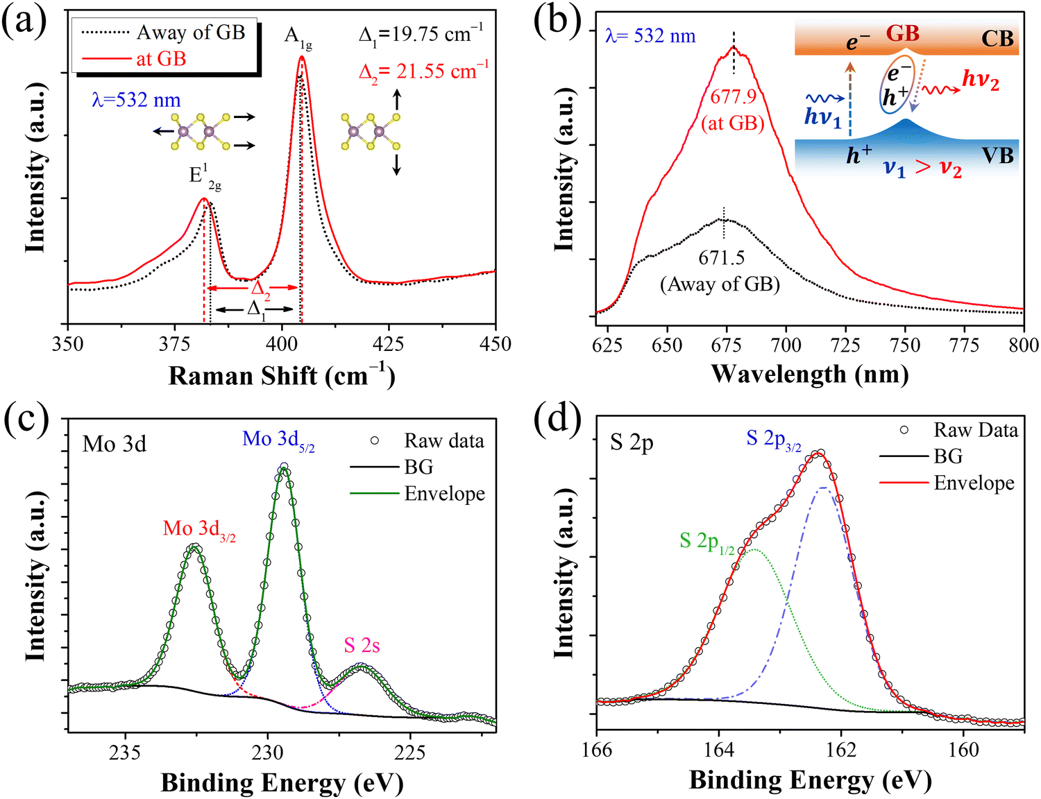 | ||
| Fig. 2 (a) and (b) Raman and photoluminescence spectra of the MoS2 sample were recorded by exciting with a light wavelength of 532 nm in the interior and at the GB. (c) and (d) High-resolution XPS spectra of Mo and S, respectively. | ||
Furthermore, we precisely examined the optical property variations of MoS2 at and away from the GB by meticulously recording the PL spectra at these specific locations, as illustrated in Fig. 2b. The emission line at the location away from the GB is observed at 671.5 nm, while it experiences a redshift to 677.9 nm at the GB. This shift indicates a reduction in the band gap at the GB of the six-point monolayer MoS2.20 Consequently, we propose a potential energy band diagram by considering the lower energy band gap at the grain boundary, as depicted in the inset in Fig. 2b, aligning with previously reported studies.31 Notably, the broader appearance of the PL spectra is attributed to the high spatial resolution of Raman microscopy. This high resolution enables the sampling of different regions within the sample, contributing to the overall spectrum.
The subsequent investigation aimed to explore the elemental composition of the six-point star monolayer (ML) MoS2 sample utilizing X-ray photoelectron spectroscopy (XPS) techniques. The recorded survey spectrum, depicted in Fig. S5a in the ESI,† comprehensively captured all major binding energy (BE) peaks corresponding to the elements molybdenum (Mo) and sulfur (S) in MoS2. To mitigate the charging effect on the sample, all associated elemental spectra underwent conventional calibration before the initiation of peak analysis using the C 1s BE peak at 284.5 eV as a reference point, originating from the presence of organic contamination. For enhanced precision, high-resolution (HR) XPS spectra were acquired for the Mo 3d and S 2p electrons, as illustrated in Fig. 2c and d, respectively. Deconvolution of the Mo 3d electron spectrum (Fig. 2c) revealed spin–orbit coupling-mediated doublet splitting, with BE peaks centered at 229.4 eV and 232.5 eV for the Mo 3d5/2 and 3d3/2 lines, respectively. Similarly, deconvolution of the HR XPS spectrum for the S 2p electrons exhibited doublet splitting under spin–orbit coupling, with BE peaks centered at 162.2 eV and 163.4 eV for the S 2p3/2 and 2p1/2 lines, respectively. The high-resolution spectrum of O 1s electrons shows a BE peak centered at 532.7 eV without any additional peak, as shown in Fig. S5b in the ESI,† which actually originates from the Si/SiO2 substrate. Importantly, all these BE positions for the elemental composition of our MoS2 sample align seamlessly with the National Institute of Standard and Technology (NIST) database.32 Thus, the growth and composition of our chemical vapour deposition (CVD)-grown ML MoS2 sample are robustly confirmed, supported by the systematic analysis conducted through XPS.
To elucidate the structure and crystal orientation of the two MoS2 domains at the grain boundary (GB) in the six-point star-shaped sample, atomic-scale investigations were conducted using a transmission electron microscope (TEM), as illustrated in Fig. 3.18,23 The low-resolution TEM image recorded near the leg region of our six-point star sample reveals the ultrathin nature of monolayer (ML) thickness without any clear signature of the GB (Fig. 3a). For a more precise investigation, a high-resolution (HR) TEM image near a GB region and a selected area electron diffraction (SAED) pattern were recorded, as depicted in Fig. 3b and c, respectively. The SAED pattern displays three consecutive encircled diffraction spots with inter-planar d-spacing values of 2.7, 1.6, and 1.37 Å. These d-spacing values were utilized to identify the lattice planes using the ICDD database PDF number 00-037-1492, corresponding to (100), (110), and (200) planes, as illustrated in Fig. 3c. The atomic packing of the six-point star MoS2 with the GB was investigated more precisely by recording the HR-TEM images of three different smaller regions marked in Fig. 3b. Interestingly, the MoS2 flake appears continuous across the GB, but the crystal plane orientation is found to be entirely different across the domains with sharp stitching.18,20 This observation signifies no discontinuity in the lattice structure within each grain at the boundary but shows a completely different orientation, as illustrated by the HR-TEM images in Fig. 3(d–f). Fig. 3d shows an HR-TEM image recorded on the left side of the GB at marked location 1 in Fig. 3b, depicting a d-spacing of 0.16 nm for the lattice plane (110). Similarly, the marked location 3 to the right side of the GB shows a d-spacing of 0.28 nm for the lattice plane (100), as shown in Fig. 3f.23 Therefore, these HR-TEM images and related analyses strongly confirm the structure of the GB at the atomic scale resolution in the CVD-grown six-point star monolayer MoS2 sample, as depicted in Fig. 3e.
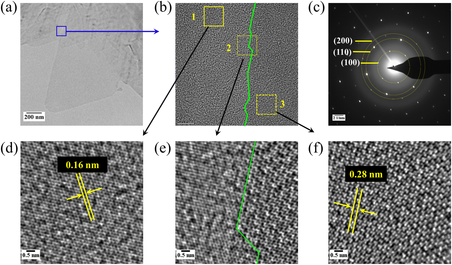 | ||
| Fig. 3 (a) Low-resolution TEM image of the six-point star of MoS2. (b) High-resolution transmission electron microscopy image of monolayer MoS2 marked three different regions across the GBs as 1, 2 and 3. (c) Selected area electron diffraction (SAED) pattern of the MoS2 sample as shown in the blue square region in (a) showing periodic bright diffraction spots similar to a monocrystalline phase. (d)–(f) HR-TEM images of 1, 2 and 3 regions, respectively. | ||
2.2. Influence of GB on optoelectronic properties of MoS2
To investigate the influence of GBs on the electrical and optoelectronic properties of ML MoS2, two planar devices were fabricated by employing a photolithography technique for patterning Cr/Au electrodes on top. Accordingly, a six-point star sample is used to fabricate a device with the specified structure: Au/GB-MoS2/Au. In this design, a GB is intentionally positioned between the electrodes, as demonstrated in Fig. 4a, utilizing an SEM image of an actual device and labelled as [A]. Conversely, another controlled device with a similar architecture to [A] is fabricated using a GB-free triangular ML MoS2 flake sample, as depicted in Fig. 4b of structure Au/MoS2/Au, and denoted as [B]. Then, these devices were characterized by measuring the current–voltage (I–V) characteristics in the ambient atmosphere by sweeping voltage from −1.0 V to +1.0 V in steps of 10 mV under both the dark and light illumination, as shown in Fig. 4c. The device [B] without GB shows a dark-to-light current ratio (Ilight/Idark) of about 105 at −1.0 V, which is reduced to 103 for the device [A]. A mild rectification is observed in the recorded dark current (Idark) for the device [B], which mostly originates from the difference of resistance between the contacts as other device parameters are symmetric. Interestingly, device [A] shows a much higher Idark than device [B], almost symmetric, which indicates the suppression of contact resistance difference in the presence of GB. This also indicates a significant contribution from the thermally generated carriers in the presence of defects and reduced band gap energy at the GBs.33 Conversely, the current under light (Ilight) is found to be much lower in [A], which again indicates the presence of additional load induced by the GB and thermal carrier-induced combination loss of photo-generated carriers. These photoconduction results clearly reflect that the GB-free MoS2 would be a better choice for high-performance photodetector design as found for the device [B].34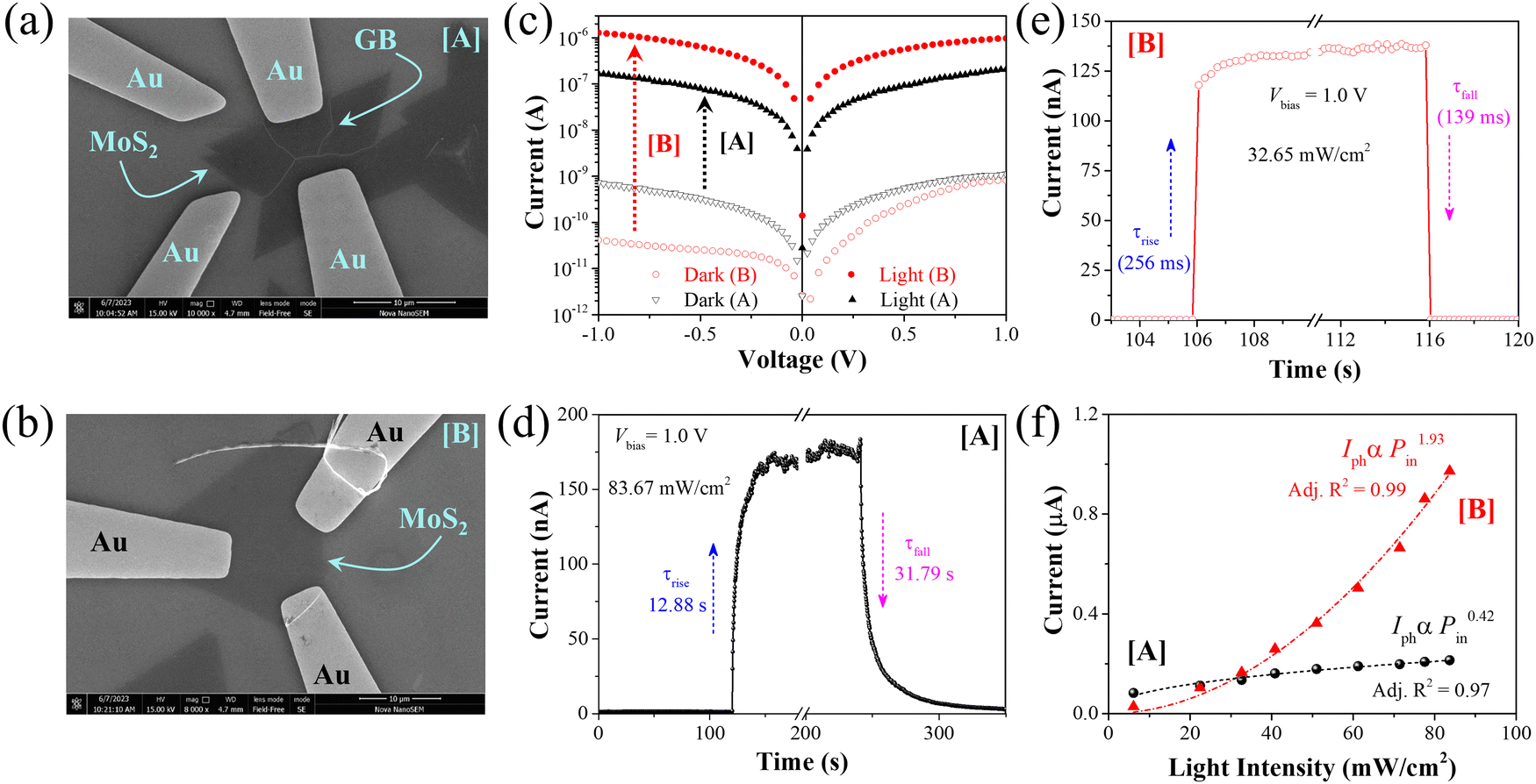 | ||
| Fig. 4 (a) and (b) Scanning electron microscopy image of devices [A] and [B] fabricated on Si/SiO2 substrates. (c) Current–voltage (I–V) characteristics of the in situ MoS2 photodetectors were recorded under ambient condition by exposing them to white light with an intensity of 83.67 mW cm−2 and in the dark. (d) and (e) Response time of devices [A] and [B], respectively, at a bias of +1 V and light intensities of 83.67 mW cm−2 and 32.65 mW cm−2. (f) Variation in the photocurrent (Iph) with light intensities. | ||
The temporal response of a photodetector is intricately linked to the dynamics of photo-generated charge carriers, wherein the electrical current through the device evolves in response to variations in the incident light illumination period. To investigate this, the temporal responses of devices [A] and [B] were documented by subjecting them to a light pulse of a specific width (tw), as illustrated in Fig. 4d and e, respectively. Notably, a significant disparity in response speed is evident in the presence of GBs in the MoS2 device. In particular, device [A] exhibits a rise time (τrise) of 12.88 s, contrasting with the 256 ms rise time for [B] in the absence of GB. Similarly, the fall time (τfall) is 31.79 s for [A] but reduces to 139 ms for [B] in the presence of a persistent photoconductive (PPC) effect in [A]. The delayed response of [A] is attributed to the slower carrier dynamics influenced by the presence of GB, which introduces defect centers that affect carrier recombination, scattering, and trapping–detrapping processes. Furthermore, the light intensity-dependent photocurrent (Iph = Ilight − Idark) responses are recorded for both devices, as depicted in Fig. 4f. These responses adhere to a power-law relationship represented by the equation Iph ∝ Pinα, where α is a constant exponent typically found to be unity or less in traditional photodetectors.33,35 For [A], the exponent value is approximately 0.42, indicating a complex photo-generated charge carrier recombination process induced by the defects in GB, as observed earlier. Conversely, [B] exhibits α value of around 1.93, suggesting the presence of a giant superlinear power law dependence of light intensity due to the photothermal effect.36,37 To highlight the performance of both devices, we conventionally estimate the responsivity (R) and specific detectivity (D*) by varying the incident light intensities, as depicted in Fig. S6 in the ESI.†38 The performance parameters for both devices are detailed in Table 1, encompassing R, D, signal-to-noise ratio (SNR), noise equivalent power (NEP), and other relevant metrics for a particular intensity of light. The significance of this work is further emphasized by comparing its performance with similar studies, as shown in Table 2. This comparison clearly demonstrates a low-voltage operation with notable photonic synaptic activities (PSA) of the lateral Au/GB-MoS2/Au device.
| Parameters | [A] | [B] |
|---|---|---|
| I dark (1.0 V) (nA) | 1.1 | 0.8 |
| I light/Idark (1.0 V) | 1.9 × 10² | 1.2 × 10³ |
| τ rise and τfall (ms) | 12880 and 31900 |
256 and 139 |
| Responsivity (R) at 83.67 mW cm−2 (A W−1) | 7.7 | 27.3 |
| Detectivity (D) at 83.67 mW cm−2 (/W) | 2.2 × 10¹⁵ | 2.3 × 10¹⁵ |
| SNR (dB) | 154.6 | 140.9 |
| NEP (×10−16 W √Hz−1) at 83.67 mW cm−2 | 27.9 | 3.8 |
| Device detail | Switching control | Rise/fall time | Operating voltage (V) | I dark (A) | I light/Idark | R (mA W−1) | D* (Jones) | PSA | Ref. |
|---|---|---|---|---|---|---|---|---|---|
| W/MoS2/p-Si (Vertical) | Optical | — | −8.0 to +8.0 | 10−8 | 3 | — | — | Yes | 39 |
| Ti/PdSe2/Au (Vertical, GB) | Electrical | — | −1.5 to +1.0 | 10−5 | — | — | — | Yes | 40 |
| Pd/MoTe2/MoS2/(Cr/Au) (Lateral) | — | — | −6.0 to +6.0 | 3.0 × 10⁻¹² | >105 | 46 | ∼109 | No | 41 |
| (Cr/Au)/n-ReS2/p-Si (Vertical) | — | 80 μs | −1.0 to +1.0 | 0.2 × 10⁻⁹ | 7.5 | 33470 | — | No | 42 |
| (Ti/Au)/MoS2/(Ti/Au) (Lateral) | Both | — | −1.5 to +1.5 | — | — | — | — | Yes | 43 |
| (Ti/Au)/SnS2/n-Si (Vertical, GB) | Electrical | — | −10.0 to +8.0 | — | — | — | — | Yes | 44 |
| Pd/ReS2/Pd (Lateral) | Optical | 33.4/36.7 (s) | −10.0 to +10.0 | 10−6 | 3 | 133.4 | 3.4 × 10⁹ | Yes | 7 |
| Au/MoS2/Au (Lateral) | Optical | 256/139 (ms) | −1.0 to +1.0 | 0.8 × 10⁻⁹ | 1.2 × 10³ | 27340 |
1.1 × 10¹² | No | This work |
| Au/GB-MoS2/Au (Lateral, GB) | Optical | 12.9/31.7 (s) | −1.0 to +1.0 | 1.1 × 10⁻⁹ | 1.9 × 10² | 7640 | 2.3 × 10¹¹ | Yes | This work |
2.3. Carrier dynamics direct evidence from electrostatic force microscopy (EFM) measurement
Exploring the impact of photo-generated carrier dynamics in illuminated MoS2 samples with and without GBs would be intriguing through direct examination using the electrostatic force microscopy (EFM) technique at the nanoscale.45 The EFM technique facilitates the measurement of the electrostatic frictional force between the sample surface and a biased atomic force microscopy (AFM) tip, which can be modulated further by applying a sample bias voltage and light illumination.21 To uncover the role of GBs in our planar MSM devices, we performed EFM testing in a combination of sample biasing and light illumination, as shown in Fig. 5a. An AFM topography image of device [A] clearly depicts the presence of GBs in the ML MoS2 sample between the two metal contacts, as shown in Fig. 5b. Fig. 5c and 5d illustrate the subsequently recorded electrostatic frictional force images in terms of EFM amplitudes under light illumination with sample biases of 0 V and 1.0 V, respectively. Notably, the image contrast of MoS2 domains is found to be uniform between the contacts at 0 V sample bias, as represented by a line profile (blue coloured), as shown in Fig. 5e, which is extracted along the shaded region shown in Fig. 5c. However, the domain contrast changed sharply upon applying a sample bias of +1.0 V. The domain near the biased electrode was much brighter than the grounded one due to the confinement of holes in the valence band by the barrier produced in the presence of GB, which is explained using the energy band diagram in the next section. The line profile (red coloured) illustrated in Fig. 5e extracted along the shaded region in Fig. 5d clearly resembles this, such as an increase in electrostatic frictional force near the biased electrode due to charge confinement in the MoS2 domain, which actually behaves as a confined charge puddle. A similar EFM study was conducted for device [B], in which Fig. 5f illustrates the AFM topography image along with the electrostatic force images at 0 V sample bias in dark and light illumination, as shown in Fig. 5g and h, respectively. The line profiles extracted from the long-shaded regions in Fig. 5g, both vertical and horizontal, are flat over the triangular ML MoS2 sample, as shown in the top panel in Fig. 5i. A similar analysis for Fig. 5h shows photo-generated charge accumulation away from the region between the electrodes, as depicted in the lower panel in Fig. 5i.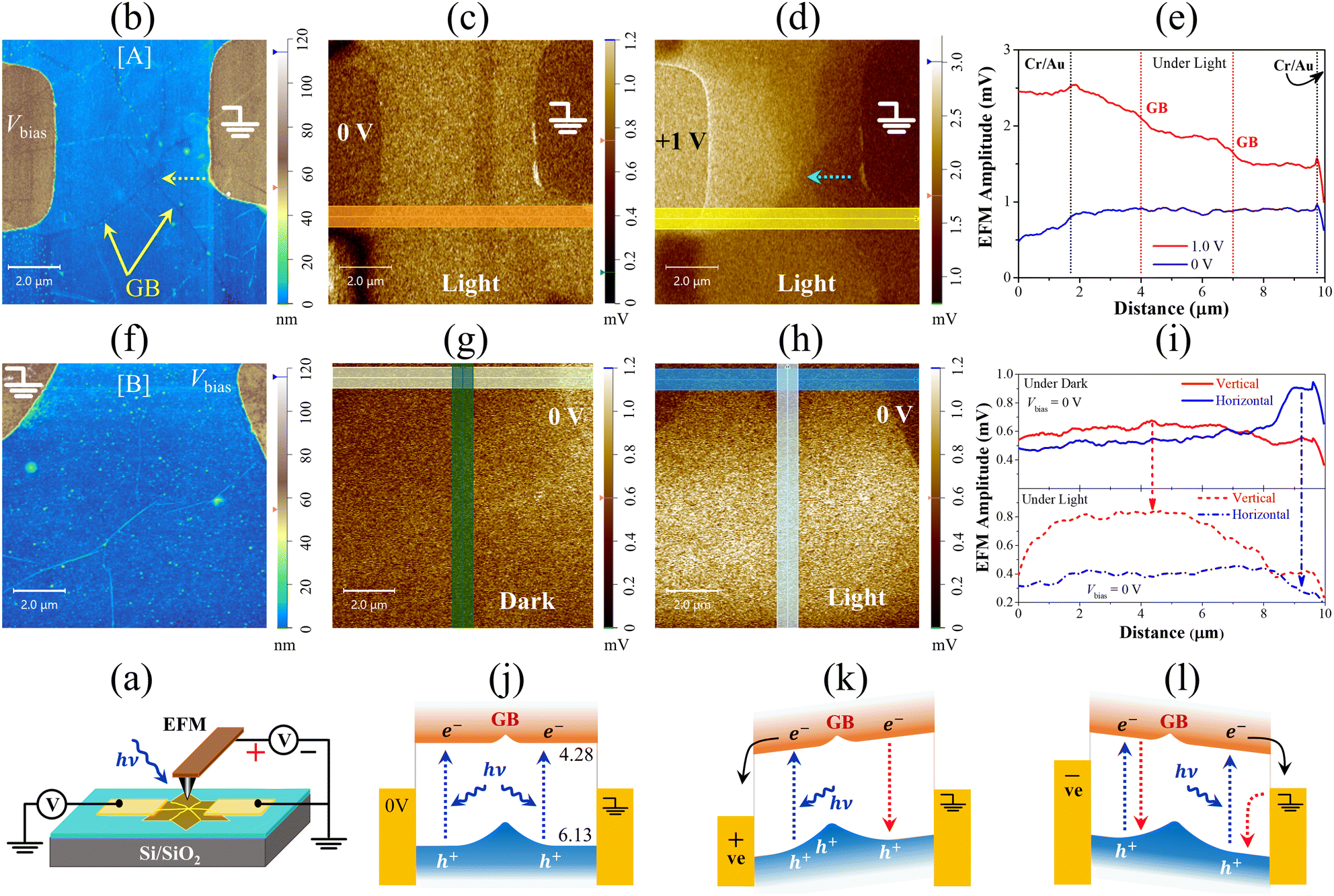 | ||
| Fig. 5 Electrostatic force microscopy (EFM) analysis of devices [A] and [B] accompanied by potential energy band diagrams corresponding to various testing conditions. (a) Schematic representation of the EFM technique with applied sample bias. (b) AFM topography image of [A] highlighting GBs with arrows and sample biasing connection by ground symbol and Vbias. (c) and (d) EFM surface potential map images of [A] under light illumination at Vbias of 0 V and 1.0 V, respectively. The arrow in (d) indicates the confluence point of multiple GBs. (e) Line profiles extracted along the marked lines on (c) and (d). (f) AFM topography of [B] highlighting sample biasing connection. (g) and (h) EFM surface potential map images of [B] under dark and light illumination at Vbias of 0 V. (i) Line profiles extracted along the marked lines on (g) and (h) under dark (upper panel) and light illumination (lower panel). (j)–(l) Energy band diagrams of [A] with no bias, positive sample bias, and negative sample bias, respectively, by including the reduced bandgap at the GB of MoS2. | ||
Further insights into the role of GBs in the electrostatic force mapping images of [A] are provided, considering the energy band diagram optimized from the photoluminescence (PL) data analysis over the GB region and away. Fig. 5j illustrates the energy band diagram with a GB at the middle for Vbias = 0 V under light illumination, which depicts photocarrier generation and recombination occurring all over the sample surface. The electrostatic force image contrast should be uniform, as shown in Fig. 5c. In contrast, Fig. 5k displays significant evidence of confining the photo-generated holes upon applying +1.0 V to the left electrode, which helps to drain out the photo-generated electrons from the left MoS2 domain, and the electrostatic force mapping image appears bright (Fig. 5d). However, the energy barrier created by the GB over the energy bands restricts electrons to cross and recombine, which makes the MoS2 domain near the grounded electrode neutral. Accordingly, the electrostatic force mapping image appeared darker in contrast. Following this convention, the contrast of both the MoS2 domains across the GB would be similar for a sample bias of −1.0 V, as illustrated in Fig. 5l, due to photo-generated charge carrier recombination in both domains. Interestingly, the EFM study under light illumination by applying a sample bias voltage of −1.0 V resulted in a similar result, as illustrated by the recorded electrostatic force images and line profiles in Fig. S7 in the ESI.† The role of GB in inducing a barrier inside the valence and conduction band for the holes and electrons is truly emphasized by our EFM results and corresponding energy band diagram analysis.21
2.4. Photonic neuromorphic developments of MoS2 photodetector
The emulation of photonic synapses represents an interdisciplinary effort at the intersection of photonics, neuroscience, and information processing, with the potential to revolutionize neuromorphic computing and related technologies.9,22Fig. 6a schematically depicts the activity of the photonic synapse in the brain, starting from the conversion of optical signal to electrical signal and subsequent modulation of synaptic connection or weight after transmission through the optic nerve between eyes and brain. A typical circuit using our Au/GB MoS2/Au photodetector for recording synaptic activities is also shown schematically in Fig. 6b, which actually replicates a biological synapse analogically. An excitatory post-synaptic current (EPSC) is a phenomenon in neuroscience that plays a crucial role in the synaptic transmission of action potential and neural communication within the nervous system. EPSCs are responsible for transmitting excitatory signals from one neuron to another through intermediate ionic events into the synaptic cleft, ultimately influencing neuronal firing and information processing in the brain.13Fig. 6c depicts a typical EPSC response recorded from our GB MoS2 device using a light pulse of the intensity of 6.12 mW cm−2 and width (tw) of 10 s in terms of measured post-synaptic photocurrent at an applied Vbias = 1.0 V. It shows a significant enhancement of the photocurrent as the post-synaptic signal during the period of the incident light pulse. Significant EPSC response modulation was observed for the same light intensity by varying the pulse period, as illustrated in Fig. S8 in the ESI.† This characteristic is essential for mimicking synaptic actions of higher orders, such as paired-pulse facilitation (PPF), spiking timing-dependent potentiation (STDP), and short- and long-term potentiation (STP and LTP).10 | ||
| Fig. 6 (a) Schematic illustration of a biological synapse analogue with the Au/GB MoS2/Au photodetector as an artificial photonic synapse in the brain. (b) Circuit connection for [A] to mimic photonic synaptic activity. (c) Recorded excitatory postsynaptic current (EPSC) triggered by a light pulse of width 10 s with an intensity of 6.12 mW cm−2. (d) Demonstration of paired-pulse facilitation (PPF) using a pair of light pulses with an intensity of 6.12 mW cm−2 and an applied sample bias of 1.0 V. Inset shows the schematic of applied paired light pulses with tw = 5 s maintaining a temporal interval Δt of 5 s. (e) PPF index as a function of time interval (Δt) between light pulses for a light intensity of 6.12 mW cm−2. | ||
PPF is a phenomenon observed in neural synapses, where the second of two closely spaced stimuli elicits a larger post-synaptic response than the first. Understanding and manipulating PPF in photonic devices could have implications for the development of optical computing, neuromorphic computing, or other advanced technologies that aim to replicate certain aspects of neural processing artificially. Fig. 6d illustrates a typical PPF response recorded using our GB MoS2 device using two consecutive light pulses of width 5 s, with a time interval gap (Δt) of 5 s between them. It shows a potentiation of the EPSC value for the second light pulse (A2) compared with the first one (A1), which is used to estimate the PPF index  for the Δt = 5 s. Accordingly, the PPF indexes were calculated for different values of Δt, as graphically depicted in Fig. 6e, which nicely follows a double exponential decay function similar to Kohlrausch law, as given below (eqn (1)):9
 | (1) |
2.5. Classical conditioning in the brain or adaptive learning
With the aforementioned advancements, devices capable of generating effects similar to classical conditioning play a crucial role in advancing our understanding of the brain. They contribute to improving therapeutic interventions, enhancing cognitive abilities, modifying behaviors, and facilitating immersive learning experiences in various domains. Classical conditioning, a form of associative learning, was systematically studied by Ivan Pavlov, a Russian physiologist, in the late 19th century. In this process, a neutral stimulus (NS) is paired with an unconditioned stimulus (UCS) to evoke a conditioned response (CR). Over time, the neutral stimulus (NS) is transformed into a conditioned stimulus (CS) capable of eliciting the conditioned response (CR).15,46 Our study, depicted systematically in Fig. 7 using the GB MoS2 optoelectronic device, parallels Pavlov's classical conditioning experiment. In Fig. 7a, the top panel illustrates a voltage pulse train (middle panel) with an amplitude of +2.0 V and a width of 2 s, serving as the NS input—analogous to the bell sound in Pavlov's dog experiment. The output, recorded as zero response (bottom panel), mimics the absence of salivation. Subsequently, light pulses (middle panel) function solely as the UCS input, akin to the presentation of food, resulting in an unconditioned response (UR) recorded in the bottom panel in Fig. 7b. Notably, the UR exhibits a significant change, reminiscent of the initiation of salivation in dogs responding to the UCS input. In the next phase, both the NS and UCS inputs are utilized to train [A], and the corresponding output records the UR. This training phase reproduces a salivation-like effect in dogs, as systematically illustrated in the panels in Fig. 7c. Finally, using the NS replicating the bell sound as the sole input yields a significant change in the output, which is identified as the conditioned response (CR). This CR is equivalent to the UR or salivation of dogs, even in the absence of food. This result indicates the successful conversion of the NS, akin to the bell sound, to a CS – equivalent to the perception of food, as depicted schematically in the top panel in Fig. 7d. Consequently, our GB MoS2 optoelectronic device successfully replicates Pavlov's dog experiment, showing its potential for designing hardware that mimics classical conditioning in the brain.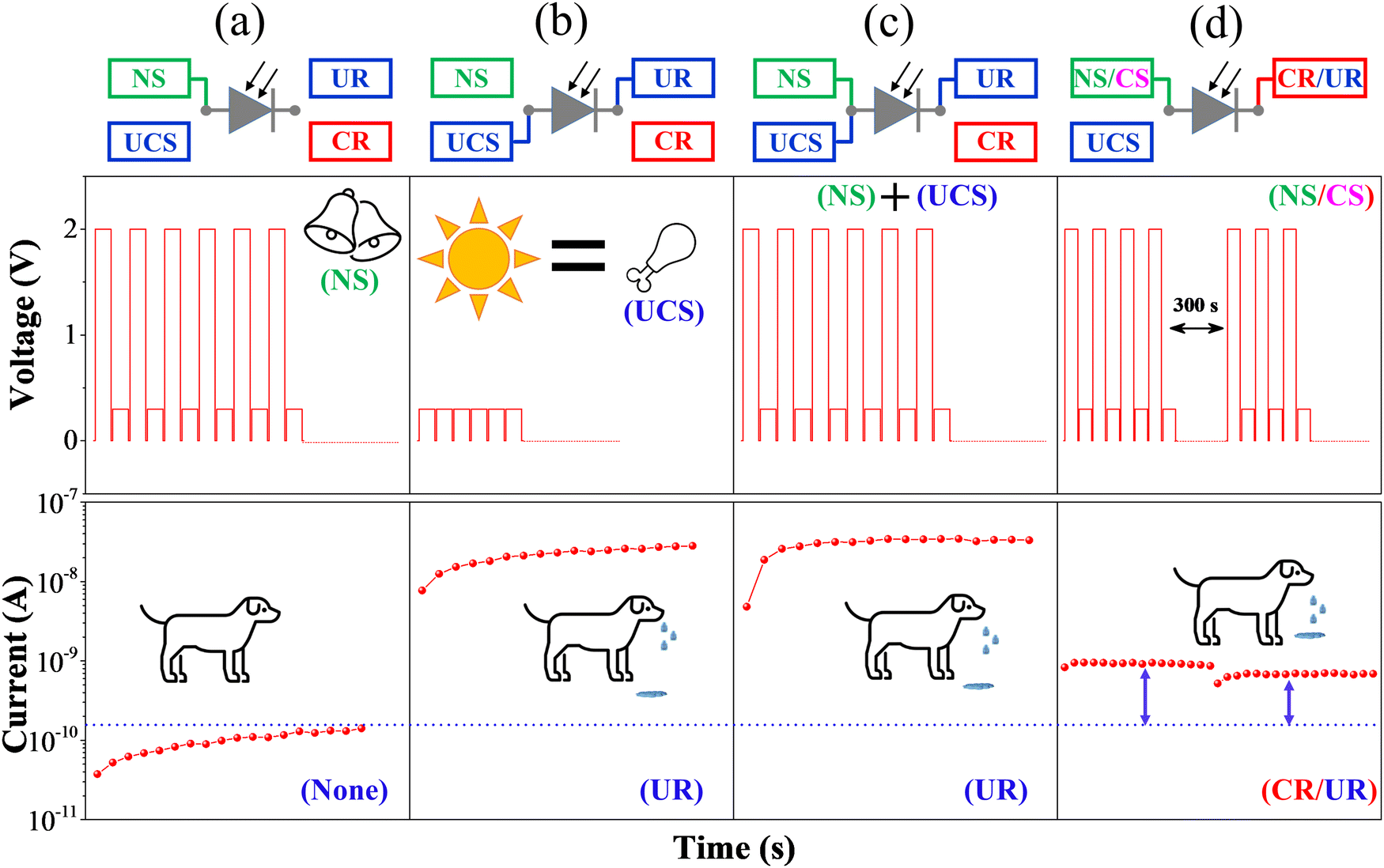 | ||
| Fig. 7 Demonstration of classical conditioning of the brain using the six-point star 2D MoS2 photodetector or [A] by mimicking Pavlov's dog experiment. The top panels outline the essential steps, showcasing potential combinations of input stimuli and resulting responses using the photodetector symbol. The middle panels depict all four combinations of stimuli, involving a bell (neutral stimulus, NS) and food (unconditioned stimulus, UCS). The bottom panels showcase the corresponding responses by recording the current at the output and parallel postures of a dog. (a) Influence of the NS on the output current. (b) Effect of the UCS. (c) Combined effects of UCS and NS. (d) Influence of NS post-training with (NS + UCS) and the transformation of NS into the conditioned stimulus (CS). | ||
3. Conclusion
In conclusion, this study highlights the transformative potential of layered 2D materials with grain boundaries (GBs) across various applications. Despite significant advancements in the field, deliberately incorporating GBs during the growth of 2D materials remains a challenge. Through our investigation into the significance of GBs in monolayer molybdenum disulfide (ML MoS2), particularly in terms of optoelectronic functionalities, such as photodetection, photonic synaptic behaviors, and brain-like adaptive learning, we reveal valuable insights. Our comparative analysis underscores the superior performance of GB-free MoS2 devices in photodetection, with remarkable characteristics, including a high dark-to-light current ratio, responsivity, detectivity, and noise equivalent power, surpassing devices containing GBs in MoS2. Additionally, our findings reveal that GBs significantly delay the response speed, indicating the presence of persistent photoconductance (PPC), which poses a major challenge for practical applications. To overcome this, further efforts are needed to enhance the response speed by optimizing the material selection and device architecture. Interestingly, we observe that GBs facilitate the emulation of various photonic synaptic behaviors and demonstrate photonic adaptive learning in MoS2, marking an early indication of this phenomenon in the literature.Furthermore, our experimental results shed light on the atomic-level structure of MoS2 domains at GBs, highlighting their role as charge carrier recombination centers due to the presence of defects. Notably, GBs induce a barrier within the energy bands by shrinking the bandgap, thereby impeding the flow of the photogenerated carriers. Through a systematic elucidation of these phenomena using energy band diagrams and visualization techniques, such as electrostatic force microscopy, our study contributes to a deeper understanding of the complex interplay between grain boundaries and optoelectronic functionalities in 2D materials. Moving forward, addressing the challenges associated with the deliberate incorporation of GBs in 2D materials and leveraging their unique properties could pave the way for the development of advanced photonic memristor devices with enhanced performance and functionality.
4. Experimental method
4.1. Materials and chemicals
Molybdenum(VI) oxide (MoO3, 99.97%), sulfur powder (S, >99.5%), sodium chloride (NaCl, >99%), 2-propanol (IPA, 99.5%), and acetone (99.5%) were purchased from Sigma Aldrich/Merck India and used as received without further purification. Si/SiO2 (300 nm) wafers, purchased from Silicon Valley Microelectronics (SVM) Inc., USA, were used as the substrate to grow monolayer 2D molybdenum disulfide (MoS2) flakes using the thermal chemical vapour deposition (TCVD) technique. Gold (Au, 99.999% purity) and chromium (Cr, 99.999% purity) were purchased from Testbourne Ltd, UK to deposit metal electrodes for electrical contacts. Deionized (DI) water from the Milli-Q Direct 8 system with a resistivity of 18.2 MΩ-cm was used to clean the substrates. Argon (Ar, 99.999% purity) was used as the carrier gas inside the CVD chamber during the growth process of MoS2 monolayer flakes.4.2. Monolayer MoS2 growth
Monolayer 2D MoS2 flakes were grown over various substrates (e.g., Si/SiO2 or quartz) using the chemical vapour deposition (CVD) method with argon (Ar) and NaCl as the transport gas agent and seeding promoter. Briefly, Si/SiO2 substrates of size 13 × 18 mm2 were cut using a diamond scriber and cleaned by following the standard protocol using ultrasonication by placing them into IPA, acetone, and DI water. The substrates were dried after cleaning under a stream of dry air and treated with oxygen (O2) plasma at a set power of 95 W using a plasma cleaner tool of model number HPT 100 procured from Henniker Plasma, UK to remove the residual organics or any other contaminants. Then, the cleaned Si/SiO2 substrates were loaded inside the CVD chamber, which was a quartz tube with a length of 1 m and an outer diameter of 80 mm, and placed on a ceramic boat kept upside down with a gap of 10 mm between the two, as illustrated schematically in Fig. S1 in the ESI.† The next step was to load the precursors S and Mo with the seeding promoter NaCl into the quartz tube of the CVD system procured from VT Vacuum Technologies (P), Ltd, Bangalore. Typically, 10 mg of molybdenum(VI) oxide powder was placed in the middle of a ceramic boat located at the center of heating zone 2 (rightmost downstream). Then, NaCl was placed in the same ceramic boat, maintaining a gap of about 10 mm upstream from the first substrate. Then, a quartz boat (L × W × H: 50 mm × 12 mm × 8 mm) carrying sulfur powder of weight 500 mg was placed inside the CVD chamber (quartz tube) at the centre of heating zone 1, maintaining a 300 mm distance from the MoO3 toward upstream. Then, the CVD chamber was sealed and evacuated for 1 hour at a pressure of 3 Torr (4 mbar). Next, the CVD chamber was purged using ultra-high pure (UHP) Argon (Ar) gas at a 500 sccm flow rate to remove the residual oxygen and moisture from the chamber. Before heating up the chamber, the deposition pressure was set to 740 Torr, with the carrier gas flow rate at 500 sccm. In the next step, the temperature of zone 2 was ramped to 375 °C at a heating rate of 15 °C min−1 from the room temperature and maintained for 30 min to reach thermal equilibrium. To initiate the monolayer 2D MoS2 growth, the heating zones were programmed in such a way that they should attain a set temperature of 600 °C, and the temperature near the sulfur source is nearing 250 °C simultaneously using a ramp rate of 5 °C min−1 and maintained to those values for 20 minutes to facilitate the MoS2 growth. During the temperature ramping process, the Ar flow inside the reaction chamber was also reduced gradually from 500 sccm to 20 sccm and was maintained for the rest of the process to cool the chamber naturally at room temperature. Then, the substrates with MoS2 flakes were removed from the chamber and used for further characterization and device fabrication.4.3. Device fabrication
The device fabrication step involved the deposition of microelectrodes (Cr/Au) using the photolithography technique on the in situ MoS2 flakes of different shapes, six-pointed star and triangular, using Heidelberg μPG 501 maskless system for writing the electrode patterns. First, monolayer 2D MoS2 deposited Si/SiO2 (300 nm) substrates were treated using SurPass 4000 as a priming agent at a spinning speed of 4000 rpm for 30 s and washed in running DI water for 60 s, followed by a drying step using nitrogen stream. Then, the SurPass-treated MoS2 sample substrates were coated with a positive photoresist (AZ 5214) layer at a spinning speed of 4000 rpm for 45 s, followed by a soft baking step at 100 °C for 60 s. After cooling, the photoresist-coated substrates were exposed to a UV laser line of 365 nm wavelength at a set power of 110 mJ for 8 s to write the desired pattern. After patterning, substrates were dipped into an MIF 726 developer solution for 20 s precisely, then rinsed with DI water and dried under N2 gas. Then, the developed patterns after a baking step (110 °C for 60 s) were inspected carefully under a microscope to confirm the high yield of pattern transfer and kept inside a thermal vacuum evaporation system (V R Technologies, Bangalore) for metallization. Finally, 80 nm thick gold (Au) with a 5 nm chromium (Cr) adhesion layer was deposited when the chamber pressure reached ∼10−6 mbar. After that, the metallized substrates were dipped into an MLO 07 stripper solution overnight for the lift-off process, which resulted in Si/SiO2 substrates with patterned electrodes on the in situ monolayer 2D MoS2 flakes.4.4. Material characterizations
Preliminary inspection of the growth of 2D MoS2 flakes and their lateral size and shape evolution was performed by recording optical images using an Olympus BX53 fluorescence microscope. Raman scattering results and photoluminescence (PL) properties, including PL and Raman mapping of in situ MoS2 flakes on Si/SiO2, were recorded under ambient conditions using a Horiba Scientific XploRA PLUS confocal Raman microscope with 532 nm laser excitation, a long working distance 100X objective (N.A 0.7), and 1800 lines per mm and 600 lines per mm gratings, with acquisition and integration time of 5 s. Excitation laser power was set to 10 mW with a spot size of 0.7 μm to record the scattering spectra of MoS2 flakes. The morphology and thickness of the MoS2 flakes were identified by recording atomic force microscope (AFM) images using JPK NanoWizard@ 4 NanoScience AFM from Germany in tapping mode with a cantilever of force constant 48 N m−1 and resonance frequency 169 KHz. Scanning electron microscope (SEM) images were also recorded using a Nova NANOSEM 450 tool to probe the morphology of CVD-grown MoS2 monolayer flakes on Si/SiO2 substrates. The X-ray photoelectron spectroscopy (Omicron nanotech XPS) technique was used to determine the elemental compositions of the CVD-grown MoS2 samples. The polycrystalline structure and grain boundaries were imaged precisely using a Titan Themis 300 kV transmission electron microscope (TEM) procured from Thermofisher Scientific, USA.4.5. Optoelectronic characterizations
Normal and transient current–voltage (I–V) characteristics under dark and light illumination for both the planer Au/MoS2/Au photodetector devices with six-pointed star-shaped and triangular flakes were recorded inside a Janis ST 500 probe station with a top quartz window and coupled with a Keithley 4200 semiconductor characterization system. An SS-F5-3A solar simulator procured from Enlitech, Taiwan was used as the light source to study the photodetection, artificial photonic synapse, and adaptive learning (classical conditioning) properties/behaviours by tuning the incident light power and irradiation width. Manually chopped light pulses were generated to record the temporal photoresponse.To demonstrate adaptive learning, we conducted trials analogically similar to the famous Pavlov's dog experiment by employing electrical pulses as the neutral stimulus (NS) and chopped light pulses as the unconditional stimulus (UCS). A Keithley 4200-SCS instrument equipped with a pulse measuring unit (PMU) was used to apply the required input electrical pulses to the photodetector device [A] or [B] (MoS2 with GB or without GB) and to measure the device current response at the output by a small reading voltage pulse. We used voltage pulses of +2 V, 1 s as the neutral stimulus (NS), followed by a reading voltage pulse of +300 mV, 1 s with a pre- and post-delay of 100 ms to record the unconditional or conditioned response (UR or CR). This was considered one cycle of training using NS, which was repeated to train the device for learning. For the unconditional stimulus (UCS), we used chopped light pulses with an intensity of 6.12 mW cm−2 and recorded the corresponding UR using read voltage pulses. Next, we used both the NS and UCS to train the device and record the response current. Finally, we used the NS only and recorded the current response similarly using read pulses as the conditioned response (CR), which is similar to UR.
4.6. Electrostatic force microscopy (EFM)
Further, we studied the effect of grain boundaries on the optoelectronic properties of MoS2 by employing dynamic contact electrostatic force microscopy (DC-EFM) using Park NX-7. A conductive probe tip ElectriMulti75-GM has an electrically conductive coating of 5 nm Cr and 25 nm Pt with a force constant (k = 3 N m−1) and resonance frequency (fresonance = 75 kHz). A drive frequency of 17 kHz with a drive amplitude of 1.0 V is applied to the tip during EFM measurements. The electrostatic friction was measured while applying 0 V, +1.0 V and −1.0 V biases to one of the electrodes, and the other electrode was grounded.Author contributions
B. C. D. and N. K. K. conceptualized the idea and designed the experiments. N. K. K. was responsible for material growth, device fabrication, and data curation. S. S. and N. K. K. jointly curated the biased EFM data. B. C. D., with the assistance of S. S. and N. K. K., analyzed the EFM data. Both B. C. D. and N. K. K. contributed to the formal data analysis and drafted the original manuscript. B. C. D. oversaw the project and secured funding. All authors were involved in the discussion of research progress, collaborated on key decisions, and collectively revised the manuscript.Data availability
The data supporting this article are included in the ESI.†Conflicts of interest
The authors declare no conflict of interest.Acknowledgements
The authors gratefully thank for the financial support from the SERB, DST, Govt. of India (Grant No. EEQ/2021/000810 and Grant No. CRG/2021/000567). A portion of this work was supported by INUP-i2i at IISc Bangalore funded by the Ministry of Electronics and Information Technology (MeitY). The device fabrication was performed using facilities at CeNSE, Indian Institute of Science, Bangalore, funded by Ministry of Education (MoE), Ministry of Electronics and Information Technology (MeitY), and Nanomission, Department of Science and Technology (DST), Government of India. N. K. K. thanks the UGC and S. S. thanks the CSIR for the fellowship support.References
- M. Y. Xu, X. R. Chen, Y. H. Guo, Y. Wang, D. Qiu, X. C. Du, Y. Cui, X. F. Wang and J. Xiong, Adv. Mater., 2023, 35, 2301063 CrossRef CAS PubMed.
- M. Vasilopoulou, A. B. Yusoff, Y. Chai, M. A. Kourtis, T. Matsushima, N. Gasparini, R. Du, F. Gao, M. K. Nazeeruddin, T. D. Anthopoulos and Y. Y. Noh, Nat. Electron., 2023, 6, 949–962 CrossRef CAS.
- D. Markovic, A. Mizrahi, D. Querlioz and J. Grollier, Nat. Rev. Phys., 2020, 2, 499–510 CrossRef CAS.
- Y. van de Burgt, A. Melianas, S. T. Keene, G. Malliaras and A. Salleo, Nat. Electron., 2018, 1, 386–397 CrossRef.
- D. Ielmini and H. S. P. Wong, Nat. Electron., 2018, 1, 333–343 CrossRef.
- S. Sagar, K. U. Mohanan, S. Cho, L. A. Majewski and B. C. Das, Sci. Rep., 2022, 12, 3808 CrossRef CAS PubMed.
- N. Krishnan K, S. Sagar, A. Mukherjee and B. C. Das, ACS Appl. Opt. Mater., 2023, 1, 759–770 CrossRef CAS.
- A. Mukherjee, K. U. Mohanan, S. Sagar and B. C. Das, Adv. Funct. Mater., 2024, 34, 2304228 CrossRef CAS.
- Y. Q. Liu, Y. H. Wu, H. J. Han, Y. Wang, R. X. Peng, K. Liu, D. Yi, C. W. Nan and J. Ma, Adv. Funct. Mater., 2024, 34, 2306945 CrossRef CAS.
- B. J. Shastri, A. N. Tait, T. F. de Lima, W. H. P. Pernice, H. Bhaskaran, C. D. Wright and P. R. Prucnal, Nat. Photonics, 2021, 15, 102–114 CrossRef CAS.
- J. Y. Mao, L. Zhou, X. J. Zhu, Y. Zhou and S. T. Han, Adv. Opt. Mater., 2019, 7, 1900766 CrossRef CAS.
- S. K. Mallik, R. Padhan, M. C. Sahu, G. K. Pradhan, P. K. Sahoo, S. P. Dash and S. Sahoo, npj 2D Mater. Appl., 2023, 7, 63 CrossRef CAS.
- J. Y. Wang, N. Ilyas, Y. J. Ren, Y. Ji, S. F. Li, C. C. Li, F. C. Liu, D. Gu and K. W. Ang, Adv. Mater., 2023, 36, 2307393 CrossRef PubMed.
- Q. H. Wang, K. Kalantar-Zadeh, A. Kis, J. N. Coleman and M. S. Strano, Nat. Nanotechnol., 2012, 7, 699–712 CrossRef CAS PubMed.
- P. Saha, E. M. Sahad, S. Sathyanarayana and B. C. Das, ACS Nano, 2024, 18, 1137–1148 CrossRef CAS PubMed.
- J. N. Coleman, M. Lotya, A. O'Neill, S. D. Bergin, P. J. King, U. Khan, K. Young, A. Gaucher, S. De, R. J. Smith, I. V. Shvets, S. K. Arora, G. Stanton, H. Y. Kim, K. Lee, G. T. Kim, G. S. Duesberg, T. Hallam, J. J. Boland, J. J. Wang, J. F. Donegan, J. C. Grunlan, G. Moriarty, A. Shmeliov, R. J. Nicholls, J. M. Perkins, E. M. Grieveson, K. Theuwissen, D. W. McComb, P. D. Nellist and V. Nicolosi, Science, 2011, 331, 568–571 CrossRef CAS PubMed.
- S. S. Wang, Y. M. Rong, Y. Fan, M. Pacios, H. Bhaskaran, K. He and J. H. Warner, Chem. Mater., 2014, 26, 6371–6379 CrossRef CAS.
- A. M. van der Zande, P. Y. Huang, D. A. Chenet, T. C. Berkelbach, Y. M. You, G. H. Lee, T. F. Heinz, D. R. Reichman, D. A. Muller and J. C. Hone, Nat. Mater., 2013, 12, 554–561 CrossRef CAS PubMed.
- S. Chen, J. Gao, B. M. Srinivasan, G. Zhang, M. Yang, J. Chai, S. Wang, D. Chi and Y.-W. Zhang, ACS Appl. Mater. Interfaces, 2019, 11, 46090–46100 CrossRef CAS PubMed.
- T. H. Ly, D. J. Perello, J. Zhao, Q. M. Deng, H. Kim, G. H. Han, S. H. Chae, H. Y. Jeong and Y. H. Lee, Nat. Commun., 2016, 7, 10426 CrossRef CAS PubMed.
- J. H. Jeong, Y. Jung, J.-U. Park and G.-H. Lee, Nano Lett., 2023, 23, 3085–3089 CrossRef CAS PubMed.
- X. Wang, B. Wang, Q. Zhang, Y. Sun, E. Wang, H. Luo, Y. Wu, L. Gu, H. Li and K. Liu, Adv. Mater., 2021, 33, 2102435 CrossRef CAS PubMed.
- W. Zheng, Y. F. Qiu, W. Feng, J. X. Chen, H. H. Yang, S. W. Wu, D. C. Jia, Y. Zhou and P. A. Hu, Nanotechnology, 2017, 28, 395601 CrossRef PubMed.
- S. S. Li, S. F. Wang, D. M. Tang, W. J. Zhao, H. L. Xu, L. Q. Chu, Y. Bando, D. Golberg and G. Eda, Appl. Mater. Today, 2015, 1, 60–66 CrossRef.
- A. W. Tsen, L. Brown, M. P. Levendorf, F. Ghahari, P. Y. Huang, R. W. Havener, C. S. Ruiz-Vargas, D. A. Muller, P. Kim and J. Park, Science, 2012, 336, 1143–1146 CrossRef CAS PubMed.
- A. W. Robertson, A. Bachmatiuk, Y. M. A. Wu, F. Schäffel, B. Rellinghaus, B. Büchner, M. H. Rümmeli and J. H. Warner, ACS Nano, 2011, 5, 6610–6618 CrossRef CAS PubMed.
- W. Zhou, X. L. Zou, S. Najmaei, Z. Liu, Y. M. Shi, J. Kong, J. Lou, P. M. Ajayan, B. I. Yakobson and J. C. Idrobo, Nano Lett., 2013, 13, 2615–2622 CrossRef CAS PubMed.
- H. Li, Q. Zhang, C. C. R. Yap, B. K. Tay, T. H. T. Edwin, A. Olivier and D. Baillargeat, Adv. Funct. Mater., 2012, 22, 1385–1390 CrossRef CAS.
- M. Kroner, A. O. Govorov, S. Remi, B. Biedermann, S. Seidl, A. Badolato, P. M. Petroff, W. Zhang, R. Barbour, B. D. Gerardot, R. J. Warburton and K. Karrai, Nature, 2008, 451, 311–314 CrossRef CAS PubMed.
- M. Tanwar, L. Bansal, C. Rani, S. Rani, S. Kandpal, T. Ghosh, D. K. Pathak, I. Sameera, R. Bhatia and R. Kumar, ACS Phys. Chem. Au, 2022, 2, 417–422 CrossRef CAS PubMed.
- Y. L. Huang, Y. F. Chen, W. J. Zhang, S. Y. Quek, C. H. Chen, L. J. Li, W. T. Hsu, W. H. Chang, Y. J. Zheng, W. Chen and A. T. S. Wee, Nat. Commun., 2015, 6, 6298 CrossRef PubMed.
- N. K. Krishnan, A. Sreedharan, S. Sagar, L. T. Manamel, A. Mukherjee and B. C. Das, Appl. Surf. Sci., 2021, 568, 150818 CrossRef.
- Q. H. Zhao, W. Wang, F. Carrascoso-Plana, W. Q. Jie, T. Wang, A. Castellanos-Gomez and R. Frisenda, Mater. Horiz., 2020, 7, 252–262 RSC.
- M. M. Furchi, D. K. Polyushkin, A. Pospischil and T. Mueller, Nano Lett., 2014, 14, 6165–6170 CrossRef CAS PubMed.
- C. L. Wang, Q. Q. Wu, Y. Ding, X. M. Zhang, W. H. Wang, X. T. Guo, Z. H. Ni, L. L. Lin, Z. Y. Cai, X. F. Gu, S. Q. Xiao and H. Y. Nan, ACS Appl. Mater. Interfaces, 2023, 15, 46236–46246 CrossRef CAS PubMed.
- J. Kang, V. K. Sangwan, H. S. Lee, X. L. Liu and M. C. Hersam, ACS Photonics, 2018, 5, 3996–4002 CrossRef CAS.
- X. H. Meng, Y. H. Du, W. B. Wu, N. B. Joseph, X. Deng, J. J. Wang, J. W. Ma, Z. P. Shi, B. L. Liu, Y. J. Ma, F. Y. Yue, N. Zhong, P. H. Xiang, C. Zhang, C. G. Duan, A. Narayan, Z. R. Sun, J. H. Chu and X. Yuan, Adv. Sci., 2023, 10, 2300413 CrossRef CAS PubMed.
- S. Sathyanarayana, N. Krishnan and B. C. Das, Phys. Rev. Appl., 2024, 21, 044015 CrossRef CAS.
- H. K. He, R. Yang, W. Zhou, H. M. Huang, J. Xiong, L. Gan, T. Y. Zhai and X. Guo, Small, 2018, 14, 1800079 CrossRef PubMed.
- Y. S. Li, L. Loh, S. F. Li, L. Chen, B. C. Li, M. Bosman and K. W. Ang, Nat. Electron., 2021, 4, 348–356 CrossRef CAS.
- Y. Chen, X. D. Wang, G. J. Wu, Z. Wang, H. H. Fang, T. Lin, S. Sun, H. Shen, W. D. Hu, J. L. Wang, J. L. Sun, X. J. Meng and J. H. Chu, Small, 2018, 14, 1703293 CrossRef.
- B. Mukherjee, A. Zulkefli, R. Hayakawa, Y. Wakayama and S. Nakaharai, ACS Photonics, 2019, 6, 2277–2286 CrossRef CAS.
- J. Jiang, W. N. Hu, D. D. Xie, J. L. Yang, J. He, Y. L. Gao and Q. Wan, Nanoscale, 2019, 11, 1360–1369 RSC.
- S. Rehman, M. F. Khan, H. D. Kim and S. Kim, Nano Energy, 2023, 109, 108333 CrossRef CAS.
- A. M. Barnes and S. K. Buratto, J. Phys. Chem. B, 2018, 122, 1289–1295 CrossRef CAS PubMed.
- H. X. Duan, L. Y. Liang, Z. D. Wu, H. B. Zhang, L. Huang and H. T. Cao, ACS Appl. Mater. Interfaces, 2021, 13, 30165–30173 CrossRef CAS.
Footnote |
| † Electronic supplementary information (ESI) available. See DOI: https://doi.org/10.1039/d4tc02912g |
| This journal is © The Royal Society of Chemistry 2024 |