 Open Access Article
The effect of oxygen on NiO as a back buffer layer in CdTe solar cells
Nicholas
Hunwick
 *,
Xiaolei
Liu
 ,
Mustafa
Togay
,
John M.
Walls
,
Jake
Bowers
,
Mustafa
Togay
,
John M.
Walls
,
Jake
Bowers
 and
Patrick J. M.
Isherwood
CREST, Loughborough University, Loughborough, UK. E-mail: n.hunwick@lboro.ac.uk
First published on 30th May 2024
Abstract
Thin film CdTe-based photovoltaic devices have achieved high efficiency above 22%. However, the device performance is limited by large open circuit voltage deficit. One of the primary reasons is non-ohmic back contacts. In this work, nickel oxide is used as a back buffer layer to form an ohmic back contact. We comprehensively investigate oxygen effects during sputtering on film properties and device performance. Increased oxygen in the deposition environment led to darker films, increased carrier concentration, decreased mobility and decreased resistivity. X-ray photoelectron spectroscopy showed peak shifts favouring Ni3+ over Ni2+, and X-ray diffraction demonstrated that crystallinity hit a peak at around 5% oxygen input. The NiO back buffer layer improves device performance by reducing barrier height at the gold back contact and improving valence band offset at the CdTe/NiO interface. The NiO layer deposited without oxygen improved the Voc to 710 mV, from a baseline of 585 mV. At 5% and 20% oxygen content during deposition, efficiency improved relative to the reference due to an increase in open circuit voltage (Voc) and short circuit current (Jsc). Voc increase is due to improved valence band offset between CdTe and NiO. The large conduction band offset also reflects minority carriers away from the CdTe/NiO interface and reduces interface recombination. SCAPS simulations demonstrated that an increase in valence band offset has shown pronounced effects of both s-kinks and rollover.
Introduction
Cadmium telluride (CdTe) is a thin film solar cell material with a direct band gap of ∼1.45 eV. It has a high light absorption coefficient of ∼104 cm−1, making it an ideal solar absorber material.1 It has successfully been commercialised by First Solar.2CdTe solar cells have seen significant performance improvement in the last decade, with the best confirmed efficiency reaching 22.4%.3 CdTe has yet to achieve its maximum theoretical efficiency of 33%.4 The primary cause is the open circuit voltage (Voc) deficit. The theoretical ideal of Voc for CdTe is ∼1.2 V, under standard conditions, whilst the cell with the highest confirmed efficiency achieved a Voc of 899.6 mV. The typically low minority carrier lifetime, low carrier density and non-ohmic back contacts are considered to be the primary reasons for the reduced Voc.4
To combat the back contact problem, buffer layers have been explored to improve CdTe device performance, with varying degrees of success. Metal oxides have frequently been employed as back buffer layers in CdTe. V2O5 was found to be effective in reducing energy barrier for hole transport.5 MoOx and WO3−x were shown to work as high work function buffer layers of CdS/CdTe thin film solar cells and were also shown to improve the Voc.6,7 Some metal oxides have shown to passivate CdTe, for instance, Al2O3 has shown to improve the minority carrier lifetime of polycrystalline CdTe.8
Nickel oxide (NiO) has been reported to improve the Voc and efficiency of CdTe when used as a back buffer layer. This improvement has been attributed to NiO being an efficient electron reflector due to the large conduction band offset, reducing recombination at the back contact.9 The application of NiO on the back of the cell, used in combination with other metal oxides, has also been shown to reduce recombination.10
Varying the oxygen in argon percentage during deposition will alter the characteristics of NiO films.11,12 For example, mobility and resistivity decrease with higher oxygen input whilst carrier concentration increases. Optical transmission and band gaps are affected by oxygen input, typically reducing in both aspects with increasing oxygen.13 NiO begins to exhibit structural changes when introducing oxygen, forming Nickel vacancies.14 These characteristic changes suggest that there is a trade-off point that should be studied with regards to its use as a back buffer layer for CdTe solar cells.
In this work, we comprehensively examine the effects of deposition environment (i.e. oxygen content in sputtering gases) on NiO thin films and back buffer layers in CdTe devices. Therefore, we can determine any device changes relative to oxygen input for NiO, and, where possible, to relate it to the innate characteristics of sputtered NiO thin films. With this information, we use SCAPS to model the device operation more accurately.
Methodology
Sample manufacture
The industry compatible method, magnetron sputtering, was used to deposit the NiO thin films and back buffer layers with the advantages of low cost, high deposition rate, film uniformity in large area and ease of use with CdTe.15 NiO films were produced using an AJA international Orion 8 HV sputter coater. It was equipped with an AJA 600 series radio frequency (RF) power supply. A commercially available 3′′ diameter preformed ceramic NiO target was used. The power density applied to the target was 3.95 W cm2. The substrates of the devices were TEC12D glass, which comprise of fluorine-doped tin oxide (FTO) and tin oxide (SnO2) coatings on glass. Samples of roughly 100 nm thickness NiO were sputtered on soda-lime glass (SLG) to characterise NiO. All substrates were ultrasonically cleaned with acetone, isopropanol, and deionised water before use. The base pressure of the chamber was at 10−7 Torr, and the substrates were rotated during deposition at 10 revolutions per minute. The NiO films were deposited at 1 mTorr working pressure of an oxygen-argon atmosphere in which the oxygen content was varied as follows: 0%, 5%, 20%, 40%, 60% and 80%.The CdTe was deposited by close space sublimation (CSS), onto TEC12D glass, with 2 mm spacing between CdTe source and glass substrate. The CSS system working pressure was 1 Torr, with some oxygen in argon atmosphere of 6%, a source plate temperature of 630 °C and substrate temperature of 515 °C. The CdTe was deposited for approximately two minutes to give a CdTe layer of 3–4 μm.
The CdTe films were then cadmium chloride (CdCl2) treated. CdCl2 was deposited by thermal evaporation in an Edwards e306 evaporator, and subsequent annealing. The annealing was carried out on a hotplate, under a fume hood, at 425 °C for a dwell time of 1 minute. The sample was subsequently quenched at 300 °C in air. After CdCl2 activation treatment, the samples were rinsed with DI water to remove CdCl2 residues. The samples were then subsequently sputter coated with a layer of 100 nm NiO, with varying deposition oxygen percentage as outlined above.
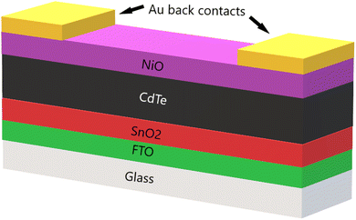
Devices were completed with 85 nm gold (Au) contacts deposited using thermal evaporation. The complete device structure, shown in Fig. 1, is as follows: glass/FTO/SnO2/CdTe (CdCl2 treatment)/NiO/Au contacts. The devices were subsequently scribed to produce an active cell area of roughly 0.25 cm2.
Characterisation techniques
The transmittance (T%) and reflectance (R%) data were obtained by spectrophotometry using a Varian Cary5000 UV-VIS-NIR Spectrophotometer. Tauc plots were employed to determine the band gaps of the NiO films using the transmittance and reflectance data. Carrier concentration, mobilities and resistivities were confirmed using a high-sensitivity parallel dipole line (PDL) hall effect system from Semilab.16 An Ambios XP-2 profilometer was used to determine the thicknesses of the samples. Carrier type was also determined by exploiting the Seebeck effect using a heated element and a multimeter. Compositional information of NiO films and valence band details were determined using a thermo scientific K-alpha X-ray photoelectron spectrometer (XPS) system, with a monochromated aluminium Kα source. High-resolution XPS scans were conducted with 50 eV pass energy, 1 eV step size, and 500 ms dwell time averaged over 5 scans for the specific Nickel, carbon, and oxygen scans. All results were charge corrected with carbon C 1s at 284.8 eV. X-ray diffraction (XRD) was used for phase determination of the NiO films, using a Bruker AXS D2 PHASER equipped with a 1-dimensional LynxEYETM detector. Measurements were done using Cu Kα X-rays with wavelength of 1.5418 Å. The current density–voltage (J–V) characteristics of devices were determined using an in-house built solar simulator under AM1.5G illumination.Results and discussion
Oxygen variation of NiO films on SLG
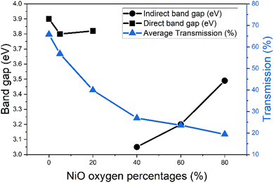
The NiO films deposited onto SLG over varying oxygen content during deposition are shown in Fig. 2. The films have a clear trend of becoming darker as more oxygen content is introduced. This darkening trend is shown clearly via its transmissivity (Fig. 3), where introducing more oxygen during deposition decreases the transmission. Without oxygen input, the films have an average transmission between 450–1000 nm of 65.8%. The transmission then steadily decreases as further oxygen is introduced. With 80% oxygen percentage, the average transmission between 450–1000 nm is 19.4%.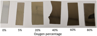 | ||
| Fig. 2 Photograph of the sputtered nickel oxide films over the varied oxygen atmospheric percentage. | ||
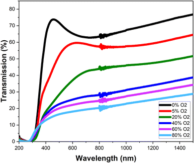 | ||
| Fig. 3 Plotted transmission percentage of the varied oxygen atmospheric percentage during deposition nickel oxide. | ||
The band gaps of the NiO films were found using the Tauc plot method17 (Fig. 4), and the calculated values are shown in Fig. 5. Also presented in Fig. 5 are the average transmissions. It has previously been presented in the literature that both indirect and direct band gaps are exhibited for NiO.18 For this investigation, direct band gap was observed at low oxygen input of 0–20%. At 40% onwards indirect was observed, suggesting there is a trade-off point of band gap structure somewhere between 20% and 40% oxygen input.
 | ||
| Fig. 4 Tauc plots with transitions of (A) direct and (B) indirect, of which oxygen during sputtering between 0–20% are direct and 40–80% indirect. | ||
It has previously been established that increasing oxygen content during NiO sputtering decreases the band gap.14 In this work, at low oxygen content, between 0% and 20%, there is a slight decrease from 3.9 eV to 3.8 eV. These values lie within the reported band gap range for direct bandgap of NiO, between 3.6–4 eV.13,19 This band gap decrease is simultaneously associated with a great decrease in transmission, which also agrees with the literature.12
The band gap decreases to 3.05 eV when it shifts to indirect, which coincides with the observed colour change of the films and continued transmission decrease. From 40% oxygen input however, the band gap increases, to 3.49 eV at 80% oxygen. The indirect bandgaps however have smaller values, compared to the direct counterparts, being between 3 eV and 3.5 eV. The reported values in the literature for indirect accept this range.18,20
The resistivity, carrier concentration, and mobility of the oxygen varied NiO films were extracted using Hall effect method and are shown in Fig. 6. The NiO films were kept to roughly 100 nm. The mobility and carrier concentration of the 0% film were immeasurable due to no proper Hall signal being detected, suggesting the sample had large resistance.
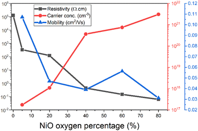 | ||
| Fig. 6 Resistivity, carrier concentration and mobility of NiO films sputtered with varied oxygen conditions. | ||
The relationship between the resistivity of the NiO films and the oxygen content of the deposition environment is that the higher the oxygen content, the lower the resistivity. 0% oxygen has a resistivity of 1.28 × 10⁵ Ω cm. At 5% the resistivity dramatically decreases to 336 Ω cm. NiO is therefore clearly sensitive to the introduction of a small amount of oxygen. From 5% it continues to decrease until it then plateaus to below 1 Ω cm from 40% onwards. The lowest the resistivity of the film was 0.0625 Ω cm, at an oxygen percentage of 80%.
The mobility of NiO has a decreasing trend with increasing oxygen present during deposition. The mobility at 5% oxygen has the maximum value of 0.1071 cm2 V−1 s−1. The mobility then sharply declines to 0.047 cm2 V−1 s−1 at 20% oxygen, but over the increasing oxygen the mobility steadily increases until 0.0311 cm2 V−1 s−1 at 80% oxygen. The carrier concentration follows an increasing trend, where at 5% oxygen input it is 1.74 × 1017 cm−3 and at 80% oxygen input it is 3.07 × 1021 cm−3. The general trends of mobility, carrier concentration, and resistivity over increasing oxygen agree with the literature.12,13
The chemical states and composition of NiO films were investigated by XPS, specifically looking at the elements of nickel (Ni) and oxygen (O). Scans of Ni 2p are shown in Fig. 7A and O 1s are shown in Fig. 7B. For the Ni 2p scan, the observed peaks across the samples found at 855 eV and at 854 eV correspond to Ni 2p3/2 levels of Ni3+ and Ni2+ ions, respectively. The peak at 861 eV is a satellite peak, and the peaks at 870 eV and 885 eV correspond to Ni 2p1/2 levels. For the O 1s scan, there are two main peaks of metal oxide at 531 eV and 529 eV corresponding to the oxygen forming with Ni3+ and Ni2+ respectively, and an organic peak at 532 eV. The binding energies of these peaks agree well with the literature.21,22
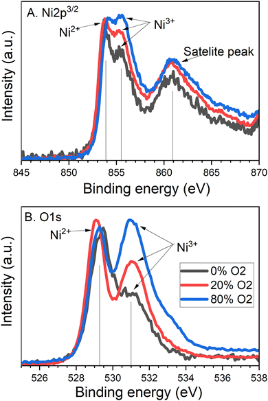 | ||
| Fig. 7 XPS plots for (A) Ni 2p3 and (B) O 1s of NiO 100 nm films sputtered with varying oxygen content. | ||
The ratio between Ni3+ and Ni2+ was calculated using the nickel XPS data scan. The 0% sample has a ratio of 0.76![[thin space (1/6-em)]](https://www.rsc.org/images/entities/char_2009.gif) :
:![[thin space (1/6-em)]](https://www.rsc.org/images/entities/char_2009.gif) 1, 5% and 20% of 0.77
1, 5% and 20% of 0.77![[thin space (1/6-em)]](https://www.rsc.org/images/entities/char_2009.gif) :
:![[thin space (1/6-em)]](https://www.rsc.org/images/entities/char_2009.gif) 1, 40% and 60% of 0.84
1, 40% and 60% of 0.84![[thin space (1/6-em)]](https://www.rsc.org/images/entities/char_2009.gif) :
:![[thin space (1/6-em)]](https://www.rsc.org/images/entities/char_2009.gif) 1 and 80% of 0.87
1 and 80% of 0.87![[thin space (1/6-em)]](https://www.rsc.org/images/entities/char_2009.gif) :
:![[thin space (1/6-em)]](https://www.rsc.org/images/entities/char_2009.gif) 1. This shows a clear increase in Ni3+ as O2 during deposition is increased and is indicated by the increasing Ni3+ peak in Fig. 7A.
1. This shows a clear increase in Ni3+ as O2 during deposition is increased and is indicated by the increasing Ni3+ peak in Fig. 7A.
With that said, a trend is observed for the XPS scan across oxygen binding energies which supports the increase in Ni3+ and therefore oxygen content present. In Fig. 7B the peaks corresponding to Ni3+ become more prominent with each iterative of oxygen content: 0%, 20% and 80%. This relationship indicates that as the proportion of oxygen in the deposition atmosphere is increased, Ni3+ becomes more favourable. The formation of Ni3+ is more appropriately understood as Ni2+ vacancies causing the adjacent Ni2+ ions to interact with the surrounding oxygen.23 The large amount of oxygen results in increased Ni2+ vacancy states in the NiO film, which would lead to a surplus of holes. Seebeck testing of the films shows p-type conduction, which further supports this conclusion. A surplus of holes will therefore account for the carrier concentration increase. The increasing Ni3+ states due to increased oxygen during sputtering also cause decreased transmission of NiO.24
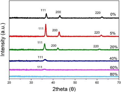
Phase identification was conducted using XRD, with the data presented in Fig. 8. The reference used was PDF 65-2901.25 Three peaks were represented throughout the varied oxygen samples: (111), (200), and (220). However, this excludes the higher oxygen content samples 40%, 60%, and 80%, whereby only (111) was represented for the 40% and 60% and no peaks for 80%. The prominence of each peak changes depending on the oxygen content. Between 0% and 5%, the maxima of the peaks increase. After 5% oxygen content, the peak maxima decrease. As the oxygen content is increased, the 2theta position of the peaks shift to the left. The attribute of decreasing peaks between 20% and 80% suggests that these samples display reduced crystallinity. On the other hand, the increasing peaks between 0% and 5% suggest the samples have become more crystalline.
Oxygen varied NiO films as back buffer layer for CdTe cells
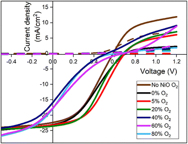
The J–V curves for the varied oxygen content buffer layers on CdTe devices are shown in Fig. 9, with the corresponding efficiency, fill factor (FF), short circuit current density (Jsc) and open circuit voltage (Voc) values shown in Fig. 10. The best cells are tabulated in Table 1. The best performing cell for the reference CdTe device without a NiO layer was 5.15%. For the CdTe devices with NiO back buffer layer of 0% oxygen, the efficiency remained similar at 5.31%. Introducing 5% oxygen during deposition was found to improve the efficiency to 6.78%. It decreases slightly to 6.3% at 20% O2. At O2 ≥ 40%, efficiency drops significantly, with the lowest being 1.66% for the 80% sample. Compared to current best performance devices, the device parameters are poor. This is most likely due to a lack of doping and Se grading.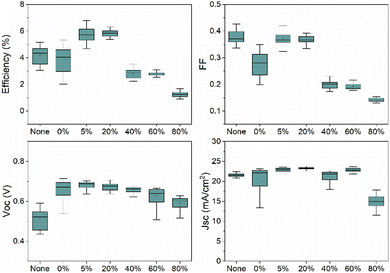 | ||
| Fig. 10 Box plots of as deposited CdTe and CdTe/NiO devices with varied oxygen during deposition of NiO films. | ||
| Sample | Efficiency (%) | FF (%) | J sc (mA cm−2) | V oc (mV) |
|---|---|---|---|---|
| No NiO | 5.15 | 39.4 | 22.4 | 585 |
| 0% | 5.31 | 32.4 | 23.0 | 710 |
| 5% | 6.78 | 41.9 | 23.1 | 699 |
| 20% | 6.30 | 39.2 | 23.5 | 683 |
| 40% | 3.50 | 24.3 | 22.4 | 643 |
| 60% | 3.10 | 20.6 | 23.7 | 636 |
| 80% | 1.66 | 15.1 | 17.8 | 620 |
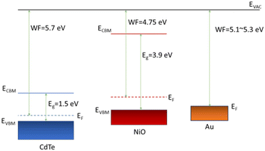
The higher efficiency is mainly due to an increase in Voc. The NiO back buffer layer with oxygen content ≤20% significantly increases open circuit voltage. The most significant increase in Voc is noted by the NiO sputtered without any oxygen present, of 710 mV. However, the FF was most prominent with the 5% and 20% oxygen during deposition samples, with both maintaining a prominent Voc of 699 mV and 683 mV. The NiO buffer layer deposited at 0% oxygen results in decreased FF because the NiO film is more resistive with immeasurable carrier concentration as aforementioned. Across the samples, the Jsc stays relatively consistent around 22.4 mA cm−2 to 23.7 mA cm−2, with a decrease at 80% to 17.8 mA cm−2. The NiO back buffer layer is used to reduce the barrier height for hole transport at the CdTe/Au interface and increase Voc (Fig. 10). This is to overcome the Schottky barrier produced at the CdTe/Au interface. It has been reported that the thermal evaporated Au contact at room temperature has a work function (WF) in the range of 5.1–5.3 eV.26–28 Additionally, CdTe has a WF of 5.7 eV,29 which creates a high Schottky-barrier height in the range of 0.4–0.6 eV for the hole transport at the CdTe/Au interface. Therefore, the high barrier height impedes hole transport and causes the strong current limiting effect (i.e., roll over) in the light J–V characteristics, which leads to decreased Voc and device efficiency. The result is consistent with previous reports.30
Fig. 11 shows the band structure at CdTe/NiO/Au. The WF of NiO deposited without oxygen during deposition was reported in the literature to be 4.75 eV.31 The WF's of NiO and gold match well to reduce the barrier height. Moreover, increasing oxygen during NiO deposition reduces the barrier height further because oxygen significantly increases carrier concentration in the NiO film, forming an ohmic contact with Au. For example, 60% oxygen in the sputtering gases leads to the carrier concentration in the order of 1 × 1020 cm−3. The extremely high carrier concentration results in a degenerate NiO film. Therefore, the barrier height becomes negligible. The introduction of oxygen during NiO deposition not only reduces the barrier height at the CdTe/Au interface but also modifies the valence band offset at the CdTe/NiO interface. Therefore, the oxygen content needs to be optimised to improve both interfaces. When the barrier height at the CdTe/Au is greatly reduced and a small barrier height does not hinder hole transport, the valence band offset at the CdTe/NiO interface dominates device operation.
The Kraut method was employed to determine the band alignment at the NiO/CdTe interface, using the respective binding energies of NiO and CdTe and the valence band maximum, the method is described elsewhere.32,33
The band offsets at the CdTe/NiO interface are tabulated in Table 2. The ΔEv decreases in the oxygen range of 0% to 20% and increases in the oxygen range of 20% to 80%. A minimum ΔEv of 0.34 eV is obtained at the 20% oxygen content. The introduced oxygen during the sputtering of NiO not only modifies the electron affinity and band gap of NiO but also shifts down the valence band maximum of CdTe due to exposure to oxygen during the sputtering process.31 The combination of these effects determines the valence band offset between NiO and CdTe. The valence band offset has a significant effect on the CdTe/NiO interface recombination and consequently affects device efficiency, wherein larger values reduce the efficiency. This work shows that valence band offset <+0.5 eV results in higher device efficiency.
| O2% | 0% | 5% | 20% | 40% | 60% | 80% |
|---|---|---|---|---|---|---|
| ΔEv (eV) | 0.47 | 0.48 | 0.34 | 0.59 | 0.52 | 0.64 |
| ΔEc (eV) | 2.86 | 2.77 | 2.65 | 2.18 | 2.21 | 2.62 |
To investigate the effect of the valence band offset at the CdTe/NiO interface, a SCAPS simulation is used to model device operation. SCAPS is a 1D simulation software developed at the University of Gent.34 The simulated device structure is SnO2:F/SnO2/CdTe/NiO/Au. The optoelectronic properties of materials in the device model are listed in Table 3. These material properties are extracted from the experiments and literature.31,34–37
| FTO | SnO2 | CdTe | NiO | Au | |
|---|---|---|---|---|---|
| W (nm) | 300 | 50 | 4000 | 100 | WF: 5.4 eV |
| E g (eV) | 3.6 | 3.6 | 1.5 | 3.9 | |
| X | 4 | 4 | 4.4 | 1.54 | |
| N A | 0 | 0 | 5 × 10¹³ | 1 × 10¹⁶ | |
| N D | 1 × 10²¹ | 5 × 10¹⁸ | 0 | 0 | |
| N t | 1 × 10¹⁴ | 1 × 10¹⁴ | 5 × 10¹³ | 2 × 10¹⁴ | |
| SnO2/CdTe interface | N t = 1 × 1012 cm−2 recombination velocity: 1 × 107 cm s−1 |
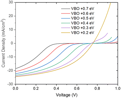
Fig. 12 shows the simulated effect of the valence band offset in the range of +0.2 to +0.7 eV. The increased valence band offset creates higher barrier for the hole transport at the CdTe/NiO interface, therefore causing stronger S-shaped kink and roll over in the light J–V characteristics as shown in Fig. 12. The increasing VBO with increasing oxygen content greatly reduce FF and efficiency, which is consistent with experimental observation. The simulated graph implies the VBO measured, between 0.34 eV to 0.64 eV, isn’t low enough to avoid the rollover observed and is a limiting factor for high performing devices.
The conduction band offset between NiO and CdTe is large. Where between 0–20% oxygen, the value lies between 2.65 eV and 2.86 eV and between 40–60% it is reduced to 2.18 eV and 2.21 eV. It increases again at 80% to 2.62 eV. The large conduction band offset would directly improve the Voc by being efficient electron reflectors, which prevents accumulation of electrons at the interface and reduces the interface recombination. The result agrees with previous work.9
Conclusions
Nickel oxide thin films of 100 nm thickness were successfully sputtered onto soda-lime glass, over various oxygen percentages during deposition, between 0–80%. Increasing oxygen content has clear effects on electrical characteristics, with decreasing mobilities, resistivities, and increasing carrier concentrations. In the high oxygen content during sputtering, the Ni3+ state becomes more favourable than Ni2+ in the NiO film. Crystallinity increases until it reaches a maximum at 5% oxygen during deposition, then decreases, with larger oxygen levels producing less crystalline films. This is caused by differing oxygen content affecting film growth.Nickel oxide of 100 nm thickness were successfully deposited onto CdTe acting as a back buffer layer. The NiO back buffer layer increases device efficiency by reducing the barrier height at the Au back contact and improving valence band offset at the CdTe/NiO interface. The introduction of NiO reduces rollover in the light J–V curve at a decreased J–V turning point. The NiO layer also leads to a large conduction band offset at the CdTe/NiO interface, therefore forming an efficient electron reflector to reduce interface recombination and increase Voc. In future work, the NiO layer will be improved, such as optimising substrate temperature during sputtering, to increase device efficiency further. On top of this, device structure will be modified to include doping such as copper or arsenic, Se grading and an improved front interface – in line with the current best performing devices.
Author contributions
Nicholas Hunwick: conceptualisation, formal analysis, investigation, visualisation, project administration, writing – original draft. Xiaolei Liu: conceptualisation, formal analysis, investigation, visualisation, writing – review & editing. Mustafa Togay: formal analysis, investigation, writing – review & editing. J. M. Walls: resources, conceptualisation, funding acquisition. Patrick J. M. Isherwood: resources, funding acquisition, conceptualisation, writing – review & editing. Jake Bowers: funding acquisition, resources, writing – review & editing.Conflicts of interest
There are no conflicts to declare.Acknowledgements
The authors would like to acknowledge LMCC for providing access to electron microscopy, XRD, and XPS, as well as Luke Jones for his assistance with XPS analysis. The work was part-funded through EPSRC grant no. EP/W00092X/1.Notes and references
- T. H. Myers, S. W. Edwards and J. F. Schetzina, J. Appl. Phys., 1981, 52, 4231–4237 CrossRef CAS.
- L. Kranz, S. Buecheler and A. N. Tiwari, Sol. Energy Mater. Sol. Cells, 2013, 119, 278–280 CrossRef CAS.
- Best research-cell efficiency chart, nrel.gov/pv/cell-efficiency.html. (accessed 24/01/24).
- R. M. Geisthardt, M. Topic and J. R. Sites, IEEE J. Photovoltaics, 2015, 5, 1217–1221 Search PubMed.
- K. Shen, R. Yang, D. Wang, M. Jeng, S. Chaudhary, K. Ho and D. Wang, Sol. Energy Mater. Sol. Cells, 2016, 144, 500–508 CrossRef CAS.
- H. Lin, I. Irfan, W. Xia, H. N. Wu, Y. Gao and C. W. Tang, Sol. Energy Mater. Sol. Cells, 2012, 99, 349–355 CrossRef CAS.
- N. R. Paudel, C. Xiao and Y. Yan, Prog. Photovoltaics Res. Appl., 2015, 23, 437–442 CrossRef CAS.
- J. M. Kephart, A. Kindvall, D. Williams, D. Kuciauskas, P. Dippo, A. Munshi and W. S. Sampath, IEEE J. Photovoltaics, 2018, 8, 587–593 Search PubMed.
- D. Xiao, X. Li, D. Wang, Q. Li, K. Shen and D. Wang, Sol. Energy Mater. Sol. Cells, 2017, 169, 61–67 CrossRef.
- P. Jundt, R. Pandey, A. Munshi and J. Sites, IEEE 48th Photovoltaic Specialists Conference (PVSC), 2021, Fort Lauderdale, FL, USA, 1614–1618 Search PubMed.
- J. Kim, Y. Ko and K. Park, Acta Phys. Pol., A, 2018, 133, 887–891 CrossRef CAS.
- H. Sato, T. Minami, S. Takata and T. Yamada, Thin Solid Films, 1993, 236, 27–31 CrossRef CAS.
- P. Salunkhe, M. A. A. V and D. Kekuda, Mater. Res. Express, 2020, 7 DOI:10.1088/2053-1591/ab69c5.
- J. D. Hwang and T. H. Ho, Mater. Sci. Semicond. Process., 2017, 71, 396–400 CrossRef CAS.
- I. V. Tudose, F. Comanescu, P. Pascariu, S. Bucur, L. Rusen, F. Lacomi, E. Koudoumas and M. P. Suchea, in Functional nanostructured interfaces for environmental and biomedical applications, ed. V. Dinca and M. P. Suchea, Elsevier, Amsterdam, 2019, ch. 2, pp. 15–26 Search PubMed.
- M. Togay, R. C. Greenhalgh, K. Morris, X. Liu, L. Kujovic, L. C. Infante-Ortega, N. Hunwick, A. M. Law, T. Shimpi, S. S. Walajabad, E. Don, G. Parada, K. L. Bath, J. M. Walls and J. W. Bowers, IEEE 50th Photovoltaic Specialists Conference (PVSC), San Juan, PR, USA, 2023, 1–3 Search PubMed.
- J. Tauc, Mater. Res. Bull., 1968, 3, 37–46 CrossRef CAS.
- A. Sawaby, M. S. Selim, S. Y. Marzouk, M. A. Mostafa and A. Hosny, Phys. B, 2010, 405, 3412–3420 CrossRef CAS.
- S. A. Mahmoud, A. A. Akl, H. Kamal and K. Abdel-Hardy, Phys. B, 2002, 311, 366–375 CrossRef CAS.
- G. Boschloo and A. Hagfeldt, J. Phys. Chem. B, 2001, 105, 3039–3044 CrossRef CAS.
- K. S. Kim and R. E. Davis, J. Electron Spectrosc. Relat. Phenom., 1972, 1, 251–258 CrossRef.
- K. S. Kim and N. Winograd, Surf. Sci., 1974, 43, 625–643 CrossRef CAS.
- J. R. Manders, S.-W. Tsang, M. J. Hartel, T.-H. Lai, S. Chen, C. M. Amb, J. R. Reynolds and F. So, Adv. Funct. Mater., 2013, 23, 2993–3001 CrossRef CAS.
- L. D’amario, R. Jiang, U. B. Cappel, E. A. Gibson, G. Boschloo, H. Rensmo, L. Sun, L. Hammarstrom and H. Tian, ACS Appl. Mater. Interfaces, 2017, 9, 33470–33477 CrossRef PubMed.
- Bruker, DIFFRAC.EVA V6, Bruker corporation, Billerica, MA, 2022.
- P. A. Tipler and R. A. Llewellyn, Modern physics, 6th edn, Freeman and Company, 2012 Search PubMed.
- K. Kim, A. S. Hyla, P. Winget, H. Li, C. M. Wyss, A. J. Jordan, F. A. Larrain, J. P. Sadighi, C. Fuentes-Hernandez, B. Kippelen, J.-L. Brédas, S. Barlow and S. R. Marder, Chem. Mater., 2017, 29, 3403–3411 CrossRef.
- W. M. H. Sachtler, G. J. H. Dorgelo and A. A. Holscher, The work function of gold, Surf. Sci., 1966, 5, 221–229 CrossRef CAS.
- A. Arce-Plaza, F. Sánchez-Rodriguez, M. Courel-Piedrahita, O. V. Galán, V. Hernandez-Calderon, S. Ramirez-Velasco and M. O. López, in Coatings and thin-film technologies, ed. J. A. Perez-Taborda and A. G. A.Bernal, Intech-Open, Rijeka, 2018, ch. 7, pp. 131–146 Search PubMed.
- S. H. Demtsu and J. R. Sites, Thin Solid Films, 2006, 510, 320–324 CrossRef CAS.
- R. Yadav, S. Patwardhan, R. J. Shourie, M. Aslam, B. Kavaipatti, D. Kabra and A. Antony, 4th IEEE International Conference on Emerging Electronics (ICEE), Bengaluru, India, 2018, pp. 1–5 Search PubMed.
- X. Liu, L. Jones, L. Kujovic, N. Hunwick, L. Infante-Ortega, M. Walls, T. Shimpi, W. Sampath, K. Barth, S. Jones, O. Oklobia and S. Irvine, IEEE 49th Photovoltaics Specialists Conference (PVSC), Philadelphia, PA, USA, 2022, pp. 0387–0389 Search PubMed.
- J. T. Gibbon, PhD thesis, University of Liverpool, 2019.
- M. Burgelman, P. Nollet and S. Degrave, Thin Solid Films, 2000, 361–362, 527–532 CrossRef CAS.
- M. Berg, J. M. Kephart, A. Munshi, W. S. Sampath, T. Ohta and C. Chan, ACS Appl. Mater. Interfaces, 2018, 10, 9817–9822 CrossRef CAS PubMed.
- L. Moulaoui, O. Bajjou, A. Najim, M. Archi and K. Rahmani, 2nd International Conference on Innovative Research in Applied Science, Engineering and Technology (IRASET), Meknes, Morocco, 2022, pp. 1–7 Search PubMed.
- S. Ahmmed, A. Aktar, M. F. Rahman, J. Hossain and A. B. M. Ismail, Optik, 2020, 223 DOI:10.1016/J.IJLEO.2020.165625.
| This journal is © The Royal Society of Chemistry 2024 |

