 Open Access Article
Creative Commons Attribution 3.0 Unported Licence
Characterization of n-doped branches in nanotree LEDs†
Kristi
Adham
 a,
Yue
Zhao
 a,
Pyry
Kivisaari
 b and
Magnus T.
Borgström
 *a
*a
aNanoLund and Division of Solid State Physics, Lund University, Lund 221 00, Sweden. E-mail: magnus.borgstrom@ftf.lth.se
bEngineered Nanosystems Group, Aalto University, Aalto, 00076, Finland
First published on 30th October 2024
Abstract
We present processed light emitting diodes (LED) devices based on GaInP core-branch nanowire (NW) structures. The LEDs rely on the charge carrier diffusion induced light emitting diode concept. The GaInP core has a higher Ga content than the branches to induce diffusion of carriers from the cores into the branches. The branches play the role of the active region in the structure, where charge carriers recombine to emit light. We investigate the impact of n-doping the branches on the performance of the LEDs. Electroluminescence measurements provide insights on the emission spectrum with varying dopant molar fraction. External quantum efficiency (EQE) measurements provide insights into the device quality, and reveal the limitations encountered in processing, such as the high sheet resistance of the indium tin oxide (ITO) transparent conductive top contact. Temperature dependent measurements allow us to probe the effect of contact resistance by measuring the I–V curve as a function of temperature. The work identifies performance limitations and paths to overcome them.
Introduction
Nanowires (NW) are promising structures for future optoelectronic devices such as solar cells,1,2 photodetectors3,4 and LEDs.5,6 Their radial strain relaxation property allows the combination of materials with a large difference in lattice constants, otherwise impossible in thin film structures.7 The field of micro-LEDs has received a lot of attention with potential applications in a multitude of categories such as displays and augmented reality/virtual reality.8–10 Furthermore, there is a need to improve the efficiency of LEDs for general lighting applications. NWs are an excellent platform to provide contributions in both areas. Recently, a new concept in LED architectures has emerged: charge carrier diffusion induced LEDs.11,12 The first experimental demonstration thereof was shown by use of thin films structures.13,14 In such an architecture, the active region is decoupled from the electrical contacts by being located on the surface of the device, instead of being sandwiched between the contact layers. The carriers are injected by bipolar diffusion in the active region upon the application of a bias. Such an architecture allows flexibility in designing the active region and avoids light being reflected from the top contact. The architecture has been taken one step further and been applied in NW structures.15 In NWs, the active region can be decoupled from the cylindrical shape of the NWs by growing branches on the sidewalls.16 The core-branch structures (hereon: nanotrees) comprise a high bandgap core material and a lower bandgap branch material to enable the diffusion of carries under forward bias. In NWs, their radial dimension plays a crucial role in the confinement of light. Below a critical thickness, the electric field extends out of the NWs physical boundaries,17 signifying an avenue to exploit for efficient light extraction even though there is a big difference between the refractive index of the semiconductor and that of air. Such a system provides the possibility to increase the light extraction efficiency by overcoming total internal reflection. Our recent studies have shown that nanotree structures can be grown with a high density of branches.16 Furthermore, we have shown the feasibility of the nanotree structures using the gallium indium phosphide (GaInP) materials system, where we obtained electroluminescence spectrum comprising of two main peaks corresponding to the core and the branch.15 In this work, we take the structure one step further and introduce doping in the branches in order to decrease the minority carrier lifetime in the branches which quickly can recombine with majority carriers. We expect the fast recombination to compete beneficially with non-radiative decay and increase the total external emission. We varied the concentration of the dopant in the branches and studied its effect of the emission spectrum. We evaluate the efficiency of the devices and provide a path to improving the performance of the devices.Experimental methods
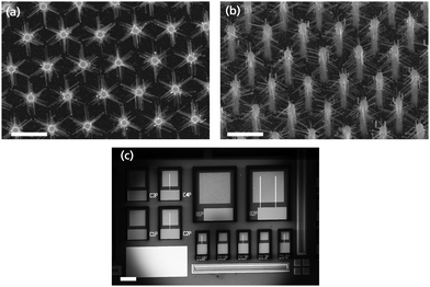
The indium phosphide (InP) substrate was decorated with gold (Au) seed particles in a hexagonal pattern with a 1 μm pitch and 150 nm diameter using Displacement Talbot Lithography, e-beam evaporation and lift-off.18 The substrates were inserted into an Aixtron 200/4 MOVPE reactor to perform the NW growth. The growth was initiated with a low temperature nucleation step at 280 °C to preserve the hexagonal pattern,19 followed by a high temperature annealing step at 550 °C to desorb the surface oxide before cooling down at the NW growth temperature at 440 °C. To grow the pin GaInP NW cores, triethylgallium (TEGa), trimethylindium (TMIn), and phosphine (PH3) were used as precursors. The total length of the NWs is 2 μm. Diethylzinc (DEZn)20–22 and tetraethyltin (TESn)23 were used as p and n-dopant, respectively. TESn was used during the intrinsic segment growth to compensate for the non-intentional p-type background doping of GaInP. Hydrogen chloride (HCl) was used to avoid radial growth.24 The grown core NWs were immersed in HAuCl4 solution to decorate the cores with Au particles via galvanic deposition.25 The Au particles act as seeds for the subsequent growth of branches. Prior to branch growth, the seed particle of the core NWs was etched away to avoid lateral growth of the cores. The substrate was coated with a photoresist, exposed in UV light, and the photoresist was developed to reveal the tips of the cores.26 A solution of potassium iodide (KI) was used to etch away the tip Au/In particles. The photoresist was then dissolved in Microposit Remover 1165 and flushed in deionized water (DI H2O). To grow the doped branches, the molar fraction of TMIn, TEGa and PH3 were kept constant for the five samples, and we varied the dopant molar fraction χ. The precursor used to n-dope the branches was hydrogen sulfide (H2S), as sulfur atoms have a similar size compared to phosphor atoms, incorporate efficiently and allows to control doping from low to high levels.23 The growth temperature was 440 °C. The full set of growth parameters for the cores and branches can be found in Tables S1 and S2 in the ESI.†Fig. 1a shows a representative scanning electron micrograph (SEM) of the nanotrees from top view. The branches are observed to have grown along the three-symmetry related 〈111〉 B directions of the cores, because of their 3-fold symmetry. Twinning in the structures, causes a 60° rotation of the crystal planes and a doubling of the branch growth directions.27 The branches have a typical length of about 200–300 nm and a diameter of 10–50 nm. In Fig. 1b a tilted SEM image is shown, revealing branch growth along the entire core structure. Fig. S1a (ESI†) shows a TEM image of the interface between a core and a branch where the propagation of lattice planes from the core to the branch is observable. Furthermore, Fig. S1b (ESI†) shows a branch where we have carried out energy dispersive X-ray (EDX) to evaluate its composition. The results are reported in Table S3 in the ESI,† where each measurement point corresponds to the points shown in Fig. S1b (ESI†). In Fig. S1c (ESI†) results from the X-ray dispersion (XRD) measurements of the as-grown core NWs to evaluate their composition is shown.The grown nanotree arrays were processed into devices using standard nanofabrication techniques. A SiOx layer was deposited via atomic layer deposition to insulate the NWs and protect them in the following processing steps. Spin coating S1818 was used as a planarization layer, and UV lithography was used to reveal the tips of the NWs.26 The SiOx was etched away from the tips by use of reactive ion etching (RIE). The NW tips were contacted by sputtering 150 nm of ITO, which serves as a top transparent contact. The processed devices are of different active region sizes, namely 100 × 100-, 200 × 200-, 400 × 400-μm2. Lastly a Ti/Au (20/400 nm) contact pad was evaporated by e-beam evaporation. Fig. 1c shows an SEM image of a portion of a processed sample with devices of each size.
For additional qualitative insight, 3D drift-diffusion simulations were carried out to study the physics of an individual model nanotree. This consisted of the core with n-, i- and p-type sections, and branches spread evenly over the i-type section. We have also carried out test simulations where some of the branches are located in the n- and p-type regions of the nanotree. Results from those simulations are not presented in this paper, but as one may expect, the further away the branch is located from the i-type region, the less it contributes to the total recombination. To limit the computational cost, a total of eighteen branches was included in the simulation. Moreover, the full nanowire array and ITO were not included in the simulation, as the purpose was to study the qualitative trends from branch doping and temperature as expected from the theory. The simulated geometry and the simulation parameters are specified in the ESI.†
Results and discussion
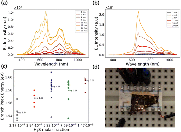
The electroluminescence spectra (EL) were measured at room temperature using an Enlitech SLI-PE-200 setup, where the devices were biased using a two-probe setup and the emitted light was collected by a microscope lens (×10, NA = 0.25), coupled to an optical fiber and analyzed by an SPR-3100-PQ spectrometer and a CCD camera. In Fig. 2a, the spectra of a 100 × 100 μm2 device from sample 1 is shown. The EL spectrum was measured from 5 V to 12 V in steps of 1 V and the reported value in the legend is the corresponding applied current through the device. The EL spectra starts to reveal emission peaks above an applied bias of 5 V, signifying high series resistance losses. At 6 V (2 mA) we can notice the onset of an emission peak at 800 nm, which originates from the branches.15 A further increase in applied bias reveals the emergence of additional peaks. The peak at 650 nm originates from the cores. Having a higher bandgap than the branches, it allows the diffusion of carriers into the branches. Initially the branch peak is higher in intensity as compared to the core, but as injection is increased, the core peak starts to dominate, resulting in a two-peak LED. The appearance of the additional peaks at higher energy, is suspected to originate from higher state transitions such as perhaps from the conduction band to the second valence band, which widens the emission spectrum, resulting in a white emission without any phosphor down conversion material. The peaks at 925 nm corresponds to the InP segment grown before switching to GaInP and 976 nm corresponds to a wurtzite–zinc blende InP emission originating from the twinned InP crystal structure.28 Increasing the dopant concentration in the branches alters the overall emission spectrum. Fig. 2b shows the EL spectra of a 100 × 100 μm2 device from sample 5 with the highest doping concentration with an applied bias from 5 to 10 V. We can observe that that the emission spectrum corresponds to white light, although the shape has slightly changed as compared to the EL spectrum in Fig. 2a. The branch and core peak have merged together and results in a single broadband emission. This indicates that doping plays an effect in the emission dynamics. Fig. S2 (ESI†) shows the measured chromaticity of a nanotree LED and compares it to the black-body locus. We observe that our LEDs have a correlated colour temperature (CCT) of approximately 3000 K. The complete set of EL spectra for samples 1–5 is found in Fig. S3 (ESI†). Although the expected explanation would be that the branch peak is blue shifting with an increased dopant concentration because of a Burstein–Moss shift,29 we do not observe this. In Fig. 2c we have plotted the branch peak energy of emission with respect to χH2S. The change in peak energy between the different samples is insignificant to be attributed to a Burstein–Moss shift. Previous research has shown that at χH2S used in this work, the structure should be degenerately doped, and we should obtain a carrier concentration in the order of 1019 cm−3 and observe a peak shift of more than 100 meV.30 On the other hand, compared to previous published work, the branches are very thin and in a high density which could influence the dopant incorporation.Fig. 2d shows an image of four devices with different active region areas biased simultaneously. The bright white light emitted from the devices supports the obtained EL spectra.
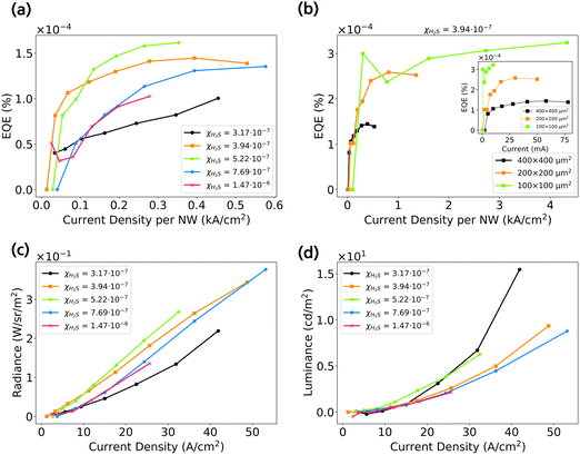
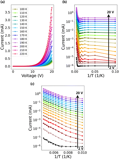
The devices have been further characterized by measuring the total radiant power and evaluating the external quantum efficiency (EQE) of the devices to reveal potential limitations in their performance. The radiant power was measured in a Thorlabs 4P3 integrating sphere coupled with a calibrated Si photodiode. In Fig. 3a we show the dependency between EQE and the current density (J) applied for samples 1–5 with an active region area of 400 × 400 μm2. The current density on the X-axis is evaluated by calculating only the current that flows through the total NW area instead of the active region area, as only the NWs provide a carrier pathway. With an increase in current density the EQE initially increases, before starting to plateau.31,32 The performance of the devices is similar for different doping concentration, indicating that the performance is mostly limited by the device processing quality. This can be observed by EQE values which are quite low as compared to other state of the art LEDs.33 This puts emphasis on improving the processing quality of the devices. As we have previously seen, the quality of the ITO plays a big role in the performance of the device.15Fig. 3b shows a comparison of EQE–J between the different active region areas for sample 2. In the inset of Fig. 3b, the EQE is plotted with respect to the total injected current in the device. We conclude that smaller active area devices perform better than the big area devices as the EQE is about 3 times higher while the injected current is 3 times lower which we attribute to the quality of the ITO. In Fig. S4 (ESI†) the comparative EQE–J for different active region area at each χH2S is shown. Furthermore, we have calculated the radiance (R), which describes the radiant power emitted from a source with area A, through a solid angle dΩ in a given direction, and luminance (L), which describes the radiance of a source weighed by the eye responsivity function Vλ, of the devices in Fig. 3c and d, respectively. Since the emission spectrum covers visible to near-IR spectrum it is more informative to evaluate both. The luminance provides information on how much of the emission resides in the visible as compared to the total emission. For example, sample 1 has the lowest radiance out of the 5 samples but has the highest luminance, signifying that it emits more strongly in the visible. In the ESI,† Fig. S5–S7 provides additional data of the LEDs at each χH2S: R–J, L–J, Radiant Power – Input Power, respectively. As we mentioned earlier, ITO has been identified as one of the bottlenecks in the device performance of the nanotree LEDs. To evaluate its effect, we have carried out temperature dependent I–V measurements. All the measurements are carried out under dark conditions. In Fig. 4a the I–V curves for a device with an active region of 200 × 200 μm2 at different temperatures are shown. The voltage is applied from 0 to 20 V with a step of 0.2 V and the corresponding current is measured. The temperature is varied from 100 K to 220 K in steps of 10 K. The full set of measurements starts from 10 K, but the I–V profile is similar for measurements between 10–100 K. The full set can be found in Fig. S8 (ESI†). The I–V characteristic shows a rectifying behaviour, typical of an LED. There is a substantial difference in the I–V behaviour with an increased temperature. At 100 K the maximum current at 20 V is on the order of 0.25 mA, while at 220 K the current reaches 3.8 mA. Low temperature leads to freezing out of charge carriers in GaInP,34 which partly can explain the I–V behaviour that we observe. We have also explored the possibility of an activation barrier at the contact interface impeding carrier injection. We have plotted in Fig. 4b a semi-log plot I–1/T, where T is the temperature. The I as a function of 1/T is plotted for current values I at every 1 V applied bias. By fitting from 100 K to 220 K as shown in Fig. 4c, we have extracted an average activation barrier of 69 meV. This value does not indicate a sufficiently large barrier that the carriers need to overcome to be injected in the NWs. An explanation for the low quality of the devices can then be attributed to the quality of the ITO itself which has a high sheet resistance and contributes to large resistive losses. We highlight that an improvement of the ITO quality is necessary to increase the efficiency of the devices.
Fig. 5a shows internal quantum efficiencies (IQEs) predicted by the simulations for the model nanotree with different surface recombination velocities (vsr), with and without doping the branches (no specification of N denotes no doping, positive N denotes donors, and negative N denotes acceptors). The surface recombination velocities have been chosen to loosely reflect the orders of magnitude reported experimentally for InP nanowires.35,36 The simulations highlight the importance of minimizing surface recombination in the branches either through passivation (targeting a smaller vsr) or through doping the branches in accordance with the experimental objectives of this work. Doping of the branches generally suppresses trap state recombination (incl. surface recombination) without harming the radiative recombination process for a given quasi-Fermi level separation in the branches, and it thereby improves the efficiency. The effect has been demonstrated through simulations for a conventional LED e.g., in ref. 37 without surface recombination considered explicitly. Studying the simulations further also reveals that simulations indicate practically ideal injection of charges from the contacts to the branches up to the onset of the efficiency droop visible in Fig. 5a. The efficiency droop in the simulations is mostly caused by electron leakage over the p-type section of the core, inflicted through the elevated voltage over the nanotree. The simulated efficiency droop could be mitigated by adding more branches in the simulations in accordance with the experimental samples. This increases the total integrated branch recombination rate at any given applied bias, and thereby decreases the share of electron leakage current that does not increase by increasing the number of branches. Fig. S9 (ESI†) shows the simulation domain for the 3D drift-diffusion simulations that were carried out.
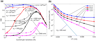 | ||
| Fig. 5 (a) Internal quantum efficiency (defined as the radiative current density divided by the total current density), simulated for the model nanotree structure with different surface recombination velocities, with and without doping the branches (no specification of N denotes no doping, positive N denotes donors, and negative N denotes acceptors). Symbols denote the operating points where the simulations were carried out, and the lines represent spline interpolations between them. (b) Total current of the model nanotree (vsr = 0 and N = 0) with the labeling of (a) simulated at different temperatures, with the applied biases given in the legend. Note that the additional voltage loss taking place in the ITO is not included in these applied biases. The dotted curve corresponds to an activation barrier of 250 meV, which provides a good agreement with the data at the smallest 1/T values. Symbols denote temperatures where the simulations were carried out, and lines represent interpolations between them. Qualitatively, the behaviour is reminiscent of the experimental data for the highest voltages in Fig. 4c the current initially decreases as a function of 1/T, but then the slope of the decrease diminishes, with the currents eventually becoming almost constant as a function of T. | ||
The temperature dependency can also be compared with the qualitative trend from the simulations of the model nanotree. Fig. 5b shows the current at selected voltages as a function of temperature. The simulations have been carried out at high injection levels with eVa (e elementary charge, Va applied bias) always more than 100 meV larger than the branch band gap at room temperature. Note that these voltages do not include the voltage loss over the ITO contact that is expected to have a major contribution in the experimentally measured voltages listed in Fig. 4. Even so, Fig. 5b exhibits certain qualitative similarities with the experimental data for the highest voltages displayed in Fig. 4c. Most importantly, the current initially decreases as a function of 1/T, but then the slope of the decrease diminishes, with the currents eventually becoming almost constant as a function of T. Exploring the simulations further shows that at the voltage where the T dependence vanishes, the quasi-Fermi level separation in the branches is larger than the band gap at all the T values studied in the simulations. In that case, even with decreasing kBT and the correspondingly diminishing Fermi–Dirac distribution width, the carrier density effectively starts to lose its temperature dependency, resulting in a constant current vs. temperature behavior. Further studies are needed to find out whether such an effect is behind the experimental curves, or whether the ITO resistance still plays a larger role.
Conclusions
In summary, we have reported on n-doped GaInP nanotree arrays for LED devices. We have processed devices of several active region areas and varied χH2S. The resulting LEDs demonstrate two main emission peaks originating from the cores and branches. Furthermore, they show a broad emission spectrum, allowing white light emission without phosphor down conversion, interesting for general lighting applications. The EQE of the devices is low, around 3 × 10⁻⁴%, highlighting the necessity to improve the device processing quality. We have attributed the problems to the quality of the ITO and further development is needed to improve processing, as well as working on passivation schemes to improve the surface recombination. Nanotree structures with an improved performance could become a strong candidate for next-generation high efficiency LEDs for general lighting and micro-LEDs.Author contributions
M. T. B. conceptualized the LED architecture, supervised the work and edited the manuscript. K. A. and Y. Z. carried out the experimental work by growing the samples, fabricating the devices, measuring and analyzing the data, and were main responsible for the writing of the manuscript. P. K. performed the theoretical simulations and contributed to the writing of the manuscript.Data availability
The data supporting this article have been included as part of the ESI.†Conflicts of interest
The authors declare no competing financial interest.Acknowledgements
This work was performed within NanoLund at Lund University. It was supported by Myfab. This work has received funding from the Swedish Research Council, the Swedish Energy Agency and the European Union's Horizon 2020 Research and Innovation Program under the Marie Skłodowska-Curie grant agreement No. 945378 and the Wallenberg Initiative Materials Science for Sustainability (WISE) funded by the Knut and Alice Wallenberg Foundation. The simulations presented in this work were carried out using the computational resources provided by the Aalto Science-IT project.References
- D. Alcer, L. Hrachowina, D. Hessman and M. T. Borgstrom, Nanotechnology, 2023, 34, 295402 CrossRef CAS PubMed.
- D. Alcer, M. Tirrito, L. Hrachowina and M. T. Borgstrom, ACS Appl. Nano Mater., 2024, 7, 2352–2358 CrossRef CAS PubMed.
- H. Jeddi, K. Adham, Y. Zhao, B. Witzigmann, F. Romer, M. Bermeo, M. T. Borgstrom and H. Pettersson, Nanotechnology, 2024, 35, 215206 CrossRef PubMed.
- H. Jeddi, M. Karimi, B. Witzigmann, X. Zeng, L. Hrachowina, M. T. Borgstrom and H. Pettersson, Nanoscale, 2021, 13, 6227–6233 RSC.
- X. Pan, J. Song, H. Hong, M. Luo and R. Notzel, Opt. Express, 2023, 31, 15772–15778 CrossRef CAS PubMed.
- Y. H. Ra and C. R. Lee, Nano Lett., 2020, 20, 4162–4168 CrossRef CAS PubMed.
- M. Björk, B. Ohlsson, T. Sass, A. Persson, C. Thelander, M. Magnusson, K. Deppert, L. Wallenberg and L. Samuelson, Nano Lett., 2002, 2, 87–89 CrossRef.
- J. J. McKendry, D. Massoubre, S. Zhang, B. R. Rae, R. P. Green, E. Gu, R. K. Henderson, A. Kelly and M. D. Dawson, J. Light Technol., 2011, 30, 61–67 Search PubMed.
- H. E. Lee, J. H. Shin, J. H. Park, S. K. Hong, S. H. Park, S. H. Lee, J. H. Lee, I. S. Kang and K. J. Lee, Adv. Funct. Mater., 2019, 29, 1808075 CrossRef.
- K. Behrman and I. Kymissis, Nat. Electron., 2022, 5, 564–573 CrossRef.
- I. Kim, P. Kivisaari, J. Oksanen and S. Suihkonen, Materials, 2017, 10, 1421 CrossRef PubMed.
- P. Kivisaari, J. Oksanen and J. Tulkki, Appl. Phys. Lett., 2013, 103, 031103 CrossRef.
- L. Riuttanen, P. Kivisaari, H. Nykänen, O. Svensk, S. Suihkonen, J. Oksanen, J. Tulkki and M. Sopanen, Appl. Phys. Lett., 2014, 104, 081102 CrossRef.
- L. Riuttanen, P. Kivisaari, O. Svensk, J. Oksanen and S. Suihkonen, Appl. Phys. Lett., 2015, 107, 051106 CrossRef.
- Y. Zhao, K. Adham, D. Hessman and M. Borgström, Nano Energy, 2024, 110400 CrossRef.
- K. Adham, Y. Zhao, L. Hrachowina, D. Alcer, R. Wallenberg and M. T. Borgström, Mater. Res. Express, 2023, 10, 085003 CrossRef CAS.
- N. Anttu and H. Xu, J. Nanosci. Nanotechnol., 2010, 10, 7183–7187 CrossRef CAS PubMed.
- L. Hrachowina, N. Anttu and M. T. Borgstrom, Nano Lett., 2021, 21, 7347–7353 CrossRef CAS PubMed.
- G. Otnes, M. Heurlin, M. Graczyk, J. Wallentin, D. Jacobsson, A. Berg, I. Maximov and M. T. Borgström, Nano Res., 2016, 9, 2852–2861 CrossRef CAS.
- M. T. Borgström, E. Norberg, P. Wickert, H. Nilsson, J. Trägårdh, K. Dick, G. Statkute, P. Ramvall, K. Deppert and L. Samuelson, Nanotechnology, 2008, 19, 445602 CrossRef PubMed.
- G. Otnes, E. Barrigon, C. Sundvall, K. E. Svensson, M. Heurlin, G. Siefer, L. Samuelson, I. Aberg and M. T. Borgstrom, Nano Lett., 2018, 18, 3038–3046 CrossRef CAS PubMed.
- J. Wallentin and M. T. Borgström, J. Mater. Res., 2011, 26, 2142–2156 CrossRef CAS.
- F. Lindelöw, M. Heurlin, G. Otnes, V. Dagytė, D. Lindgren, O. Hultin, K. Storm, L. Samuelson and M. Borgström, Nanotechnology, 2016, 27, 065706 CrossRef PubMed.
- M. T. Borgström, J. Wallentin, J. Trägårdh, P. Ramvall, M. Ek, L. R. Wallenberg, L. Samuelson and K. Deppert, Nano Res., 2010, 3, 264–270 CrossRef.
- S. Y. Sayed, F. Wang, M. Malac, P. Li, D. Wang and J. Buriak, CrystEngComm, 2012, 14, 5230 RSC.
- Y. Zhang, Y. Chen, L. Hrachowina, C. Sundvall, I. Åberg and M. Borgström, IEEE 46th Photovoltaic Specialists Conference (PVSC), 2019.
- L. S. Karlsson, M. W. Larsson, J.-O. Malm, L. R. Wallenberg, K. A. Dick, K. Deppert, W. Seifert and L. Samuelson, NANO, 2006, 1, 139–151 CrossRef CAS.
- S. Mukherjee, N. Nateghi, R. M. Jacobberger, E. Bouthillier, M. De La Mata, J. Arbiol, T. Coenen, D. Cardinal, P. Levesque and P. Desjardins, Adv. Funct. Mater., 2018, 28, 1705592 CrossRef.
- J. Wallentin, K. Mergenthaler, M. Ek, L. R. Wallenberg, L. Samuelson, K. Deppert, M.-E. Pistol and M. T. Borgstrom, Nano Lett., 2011, 11, 2286–2290 CrossRef CAS PubMed.
- D. Lindgren, O. Hultin, M. Heurlin, K. Storm, M. T. Borgström, L. Samuelson and A. Gustafsson, Nanotechnology, 2015, 26, 045705 CrossRef CAS PubMed.
- N. I. Bochkareva, Y. T. Rebane and Y. G. Shreter, Semiconductors, 2014, 48, 1079–1087 CrossRef CAS.
- G. Verzellesi, D. Saguatti, M. Meneghini, F. Bertazzi, M. Goano, G. Meneghesso and E. Zanoni, J. Appl. Phys., 2013, 114, 071101 CrossRef.
- A. Pandey, Y. Xiao, M. Reddeppa, Y. Malhotra, J. Liu, J. Min, Y. Wu and Z. Mi, Appl. Phys. Lett., 2023, 122, 151103 CrossRef CAS.
- S. D. Kwon, H. K. Kwon, B. D. Choe and H. Lim, Appl. Phys. Lett., 1995, 67, 2533–2535 CrossRef CAS.
- H. J. Joyce, J. Wong-Leung, C. K. Yong, C. J. Docherty, S. Paiman, Q. Gao, H. H. Tan, C. Jagadish, J. Lloyd-Hughes, L. M. Herz and M. B. Johnston, Nano Lett., 2012, 12, 5325–5330 CrossRef CAS PubMed.
- S. Münch, S. Reitzenstein, M. Borgström, C. Thelander, L. Samuelson, L. Worschech and A. Forchel, Nanotechnology, 2010, 21, 105711 CrossRef PubMed.
- O. Heikkilä, J. Oksanen and J. Tulkki, J. Appl. Phys., 2009, 105, 093119 CrossRef.
Footnote |
| † Electronic supplementary information (ESI) available. See DOI: https://doi.org/10.1039/d4ya00414k |
| This journal is © The Royal Society of Chemistry 2024 |

