DOI:
10.1039/D4YA00436A
(Paper)
Energy Adv., 2024,
3, 2200-2211
Microreactor assisted soft lithography of nanostructured antimony sulfide thin film patterns: nucleation, growth and application in solid state batteries†
Received
1st July 2024
, Accepted 11th August 2024
First published on 12th August 2024
Abstract
This study explores the microreactor-assisted soft lithography (MASL) method for direct, one-step synthesis and patterning of additive-free antimony sulfide (Sb2S3) nanostructured thin films. The results reveal the steady state process and its ability to overcome the challenges and limitations of conventional solution deposition processes. This new approach, exploiting continuous flow, prevents the dissolution of the growing film, a common issue in batch solution deposition methods. Furthermore, this study successfully fabricates functional Sb2S3–Li coin cell prototypes, demonstrating stable specific capacities of 600 mA h g−1 for over 260 cycles at a C/2 charge rate and coulombic efficiencies of 96–98%.
Introduction
Nanostructured antimony sulfide (Sb2S3) offers remarkable optical and electrochemical qualities such as a wide band gap (1.7–1.9 eV), high visible light absorption coefficient (∼105 cm−1), and high theoretical specific capacity (946 mA h g−1).1,2 Furthermore, Sb2S3 is cheaper and environmentally benign. For these reasons, it is one of the most sought-after materials for photovoltaic and battery applications.1,3,4 Traditional nanoparticle (NP) synthesis methods such as hot-injection,4 hydrothermal,5 solvothermal,6 and microwave irradiation7 have commonly been used to synthesize Sb2S3 nanoparticles (NPs). These nanoparticles are formulated into inks/slurries for practical applications and then used to deposit or pattern thin films.7,8 Many deposition methods such as thermal evaporation (TE),9 chemical vapor deposition (CVD),10 vapor transport deposition (VTD),11 pulsed laser deposition (PLD)12 and chemical bath deposition (CBD)13,14 offer the added advantage of growing nanostructured thin-films directly on substrates. While TE, PLD, VTD, and CVD are gas-phase deposition methods, CBD is a liquid-phase technique. For applications where minimizing layer thickness and device size is essential, gas phase methods provide a lower growth rate than solution-based processes. This method stems from gaseous reaction methods having diluted precursor vapors in carrier gas streams. However, solution-based deposition methods are more attractive for applications with higher electrode mass loading to reach significant device functionality. This advantage includes instances where relatively thicker nanostructured films, such as batteries, are needed due to their scalable and cost-effective nature and higher growth rates.15,16
Therefore, CBD is generally considered a low-cost, scalable approach for fabricating thin films over large surface area substrates based on the need for higher active material output.17,18 Sb2S3 thin films have been deposited using CBD at low temperatures, such as 10 °C to 70 °C.14,17–19 The resulting amorphous films can be thermally processed to achieve crystalline films. The CBD film characteristics can be manipulated by controlling deposition time, bath temperature, and precursor ratios. The solution-based design of CBD does correlate to a higher thin film growth rate than CVD. However, one of the difficulties of CBD is ensuring homogenous mixing for large-area films. Non-uniform growth and nucleation conditions become challenging to control, explicitly impacting the quality and reliability of process execution. CBD is also a batch method, and since the reactants are consumed over the reaction time, they must be replenished frequently. The critical factors in controlling batch Sb2S3 deposition characteristics are reaction time, temperature, mass fraction, and binding agents.
Microreactor-assisted nanomaterial deposition (MAND) enables a potential manufacturing opportunity to transition active material deposition and growth methods to more controlled and scalable processes. It is a solution-based continuous flow method of synthesizing and depositing nanostructured thin films.20,21 MAND was initially developed to manufacture semiconductor materials for photovoltaics, thin-film electronics, and anti-reflective coatings to lower process barriers to scalable nanomanufacturing.22–26 However, the resulting thin film characteristics and high process controllability potentially enable further MAND application in the emerging solid-state battery industry. The thin film characteristics can be controlled by adjusting the precursor flow rates, precursor concentrations, substrate temperature, reaction bath temperature, reaction residence, and deposition time.21,27,28
Furthermore, this method, combined with soft lithography termed MASL, allows the direct patterning of films without the assistance of additives.29 The precise patterning of electrolytes ensures optimal interface contact and uniform ion distribution, which is critical for enhancing performance and reliability.30–34 This allows on-site nanomanufacturing and patterning in a single-step process.
This work aims to develop MASL for growing additive-free nanostructured Sb2S3 thin films via reactor design, fabrication, and systematic characterization to investigate the nucleation and growth mechanisms of Sb2S3. We then demonstrate the potential of MASL in fabricating nanostructured solid-state electrolytes directly on current collectors and evaluate its electrochemical performance.
Experimental approach
Finite element analysis and pattern molds
COMSOL Multiphysics® software was used for finite element analysis (FEA) and computational fluid dynamics (CFD) during the experimental design process. CFD models were used to simulate, design, and predict multiple experimental configurations for different flow rates, substrate temperatures, bath temperatures, and microchannel designs. Heat transfer in solids and fluids and laminar flow physics were used to solve the heat and Navier–Stokes equations.
Autodesk Fusion 360 was used to model polydimethylsiloxane (PDMS) pattern molds. The CAD files were exported and 3D printed using a consumer-grade masked stereolithography apparatus (mSLA) 3D printer. Three main patterns were developed: a growth mechanism analysis pattern, a coin cell pattern, and an optical properties pattern.
Substrate preparation
The 25 mm × 75 mm × 1 mm glass substrates were mounted directly into the reactor and did not require additional preparation. The copper (EQ-bccf-9u) and aluminum (EQ-bcaf-15u-280) foil substrates were sourced from MTI and cut into 22 mm × 70 mm rectangular sheets. Polyimide tape was used to mount the foils’ polished or rough side to a 25 mm × 75 mm × 1 mm glass slide. The glass substrates were cleaned by first immersing in a 1 M NaOH bath for 20 minutes, followed by multiple rinses of acetone, methanol, and deionized water (DIW), and the substrates were dried using compressed nitrogen. The copper and aluminum foil substrates were first cleaned using dilute HCl to remove the native oxide layer. Multiple cycles of acetone and DIW rinses were then used to remove any dissolved compounds and dried with compressed nitrogen.
PDMS channel fabrication and reactor assembly
The microchannels were created using a modular polymer casting method. Different channel designs were 3D printed within a container frame using ELEGOO Mars mSLA 3D printer with translucent ELEGOO 3D standard photopolymer resin. The printer settings were a layer height of 0.05 mm, first layer exposure of 70 s, layer exposure of 5.5 s, and 405 nm excitation. The resulting printed molds were filled with PDMS resin and allowed to polymerize for 48 hours. Once fully cured, the cast part was removed and cleaned using 2-propanol. This process (Fig. S1, ESI†) was repeated for each channel design.
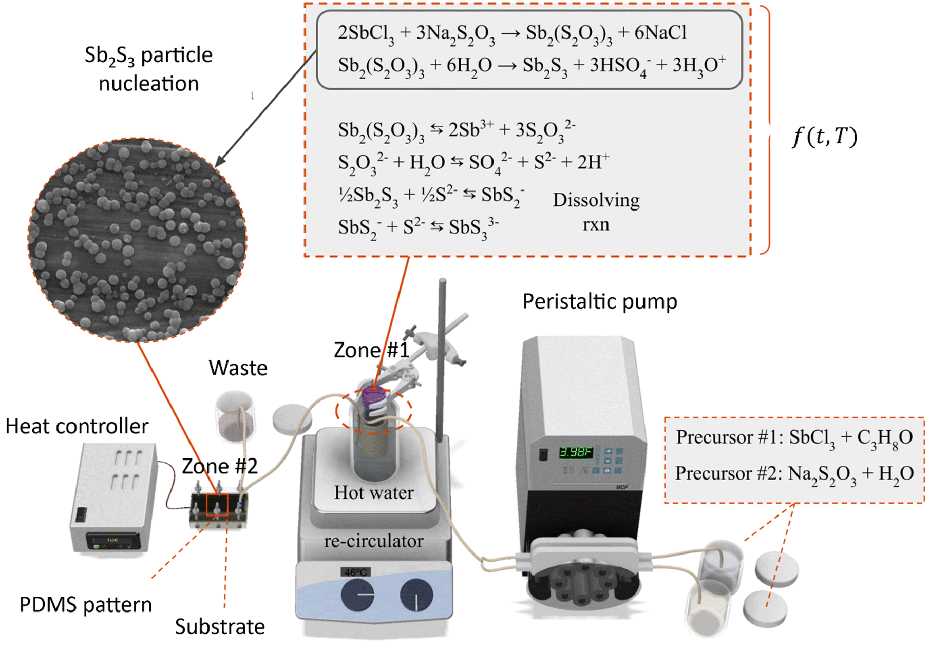
Fig. 1 shows the exploded view of the MASL reactor. The design of all the components is stacked vertically like a sandwich and aligned using six M4 screws. This design ensures that the compressive force holding the PDMS seal does not change over time during an experiment. Furthermore, the stacked layout and wingnuts make for easy assembly and disassembly of the reactor during each experiment. This feature also made replacing broken components quick and easy. The materials selected for each component were based on chemical resistance, thermal conductivity, and cost-effectiveness. The ¼-28 threaded connectors (UX-02019-42) were sourced from Cole–Palmer and mounted the 18-gauge blunt tip dispensing needles that connected to the feeding tube.
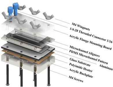 |
| | Fig. 1 Exploded view of MASL reactor. | |
Precursor preparation
The precursors used are based on a variation of the procedure reported by Nair et al.18 and were adapted to make it viable in a continuous flow reactor setup. In one beaker, 3.1622 g of Na2S2O3 was sonicated in 80 mL of deionized H2O. 0.4562 g of SbCl3 was sonicated in an 80 mL 2-propanol separate beaker. The resulting molarities are 0.25 M Na2S2O3 solution and 0.025 M SbCl3 solution. The volume of the solution was scaled depending on the flow rate and deposition time parameters.
Sample fabrication
The substrates were installed into the reactors along with the PDMS pattern and compressed using the screws to form a seal with the injectors. The two precursors at 20 °C were fed into the peristaltic pump at a flow rate of 2.5 mL min−1 and combined using a t-mixer before entering the 35 °C water bath. The tubing's inner diameter was 2 mm. The tubing length inside the water bath was 3 meters, and the outlet was connected directly to the MASL reactor, as shown in Fig. 2. The process can be divided into two main zones. Zone #1 is the heated bath, wherein the SbCl3 reacts with the Na2S2O3 to form Sb2(S2O3)3, which subsequently hydrolyzes to form Sb2S3. In this zone, homogeneous nucleation and heterogeneous nucleation of Sb2S3 spherical nanoparticles occur at 35 °C. Zone #2 is the MASL reactor, wherein the Sb2S3 can reduce its Gibbs free energy by nucleating on the substrate. This results in a thin film and grain growth over time. Varying temperatures of the substrate were investigated, ranging from 10 °C to 80 °C. Varying deposition times were investigated, ranging from 5 to 120 minutes. After the deposition time was executed, the sample was removed from the reactor, thoroughly rinsed using DIW, dried using nitrogen, labeled, and stored for characterization. The detailed sample fabrication steps are shown in Fig. S2, ESI.†
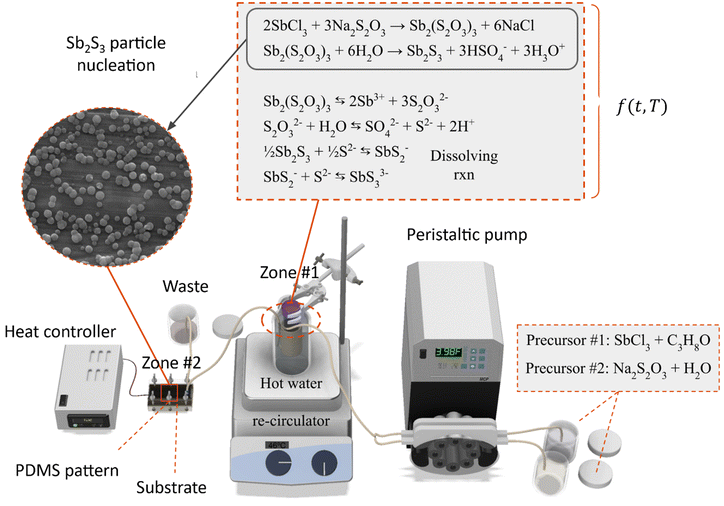 |
| | Fig. 2 Process schematics for Sb2S3 thin films. | |
Characterization methods
The film thicknesses were measured using a Veeco Dektak 8 stylus profilometer with a moving contact probe to scan the surface. FEI Quanta 600 SEM with energy dispersive spectroscopy (EDS) detector was used to image the samples’ surface morphology and elemental composition. The crystal structure of Sb2S3 was analyzed by X-ray diffraction (XRD) with Rigaku SmartLab X-ray diffractometer utilizing Cu-Kα radiation. GSAS 2, VESTA, and the crystallography open database (COD) were used to process the diffraction data and determine crystal structure, lattice parameters, and crystallite size. The JASCO V-670 UV-vis/NIR spectrometer was used to measure how much a sample absorbs regions of the visible and ultraviolet spectrum. Tauc plot was used to calculate the band gap. The cyclic voltammetry (CV) tests were conducted on a CH Instruments 760E potentiostat. The galvanostatic charge/discharge curves were tested at room temperature on a Landt battery tester (CT2001A).
Results and discussions
Simulation results
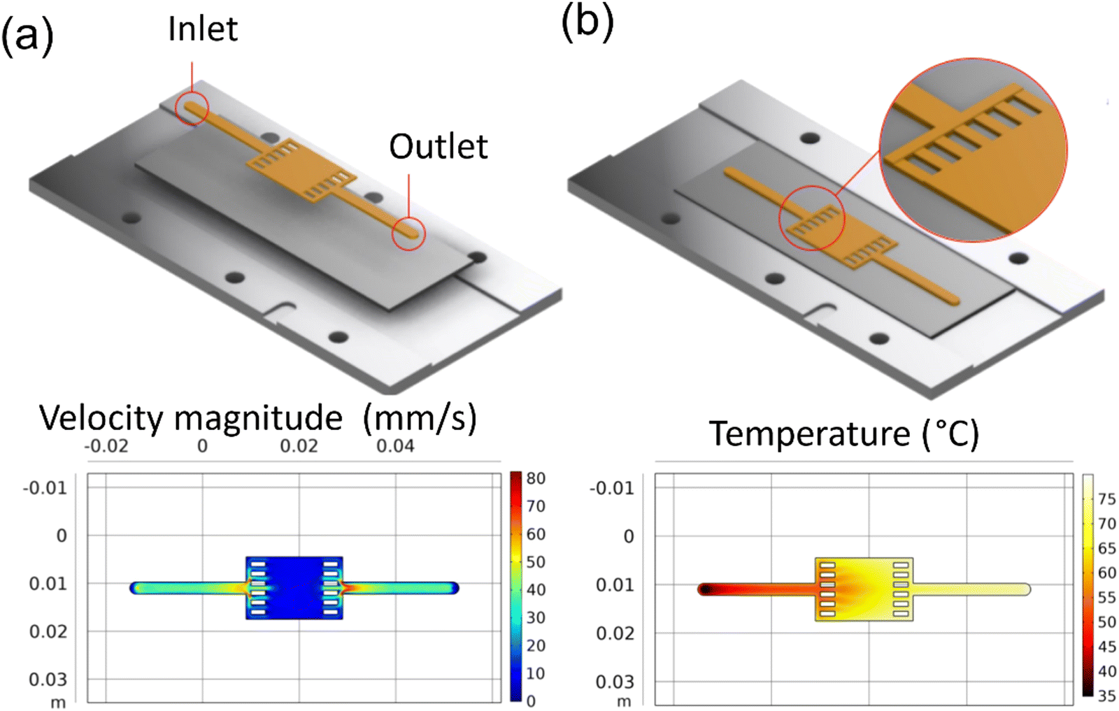
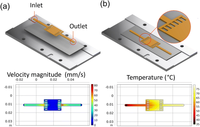
A single channel pattern was used to collect velocity samples. Other investigators have used this pattern in their studies on ZnO and CuO.29 The COMSOL simulations, as seen in Fig. 3a and b, show the uniform velocity across the deposition surface and the temperature gradient concerning residence time in the channel. This pattern was used to collect data on the effect of residence time and temperature on the Sb2S3 thin films. The samples collected from this pattern helped investigate the growth mechanisms and allowed failure modes to be identified and resolved before device samples.
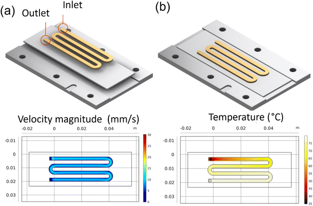 |
| | Fig. 3 COMSOL simulation results for reaction inlet velocity of 14.9 mm s−1 at 35 °C on an 80 °C heating plate: (a) the velocity profile at center line, (b) the surface temperature. | |
A coin cell pattern was also developed for galvanostatic and cyclic voltammetry tests. This pattern yielded three coins, which were later hole-punched for testing. Both flow rate and thermal analysis were conducted and presented in Fig. 4a and b.
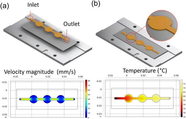 |
| | Fig. 4 COMSOL simulation results for reaction inlet velocity of 14.9 mm s−1 at 20 °C on an 80 °C heating plate: (a) the velocity profile at center line, (b) the surface temperature. | |
A wider film pattern was also designed and simulated for larger surface area applications. UV-vis-NIR spectroscopy characterization used this pattern. The COMSOL simulations (Fig. 5a and b) show that the velocity profile is uniform in the wide deposition area and shows a similarly expected gradient in the temperature profile.
 |
| | Fig. 5 COMSOL simulation results for reaction inlet velocity of 44 mm s−1 at 40 °C on a 90 °C heating plate: (a) the velocity profile at the center line, (b) the surface temperature. | |
It can be observed that all the patterns show similar behavior in terms of flow and temperature profile. The velocity is uniform across and along the length of the patterns. However, there is variation in the temperature along the length of the patterns. This result is attributed to the longer residence time that heats the solution as it flows along the length. The uneven temperature distribution leads to different reaction rates and, thus, different deposition rates.21,29 The phenomenon was also observed in our experiments. The fabricated sample's optical image (Fig. S2, ESI†) shows a lighter color at the beginning of the pattern and darker downstream, indicating lower film thickness at the start of the channel. This issue may be solved using localized heating or gradient heating of the channel to maintain the same solution temperature along the channel's length.28,35,36 However, this is not the scope of this work and is not implemented in this current work. All the studies were performed using a global substrate heater.
Investigation of nucleation and growth
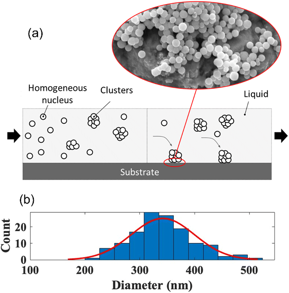
Homogeneous nucleation.
The homogeneous nucleation of Sb2S3 occurred in zone 1 and zone 2 of the system, as sketched in Fig. 6a and validated using the SEM images. The SEM images also indicate spherical nuclei growing in the bulk liquid and forming clusters before gravity depositing onto the substrate. Homogeneous nucleation occurs in both zones since the process is spontaneous and random in the liquid based on the reduction of Gibbs free energy of the system. There is a balance between the driving force and energetic barriers to homogeneous nucleation, which can be described as a total change in the Gibbs free energy to form the solid nuclei as a function of the spherical nuclei radius, which is described in eqn (1).37| | | ΔG(r) = VnucleiΔGV + AnucleiγSL = (4/3)πr3ΔGV + 4πr2γSL | (1) |
| | | r* = −2γSL/ΔGV = −2γSLTm/ΔHfΔT | (3) |
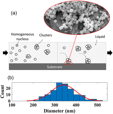 |
| | Fig. 6 (a) Homogeneous nucleation Sb2S3 nanoparticles and (b) size distribution. | |
γ
SL is the interfacial free energy between the solid and liquid Sb2S3. ΔGV is the change of Gibbs free energy per unit volume of the solid phase. ΔHf is the latent heat of fusion. ΔT is the undercooling. Anuclei is the surface area of contact between the nuclei and liquid. Vnuclei is the volume of the nuclei.
The critical radius for which the homogenous nuclei do not dissolve back into the liquid can be found by taking the derivative of eqn (1) with respect to the radius and solving for the radius when set to zero. The critical radius of the Sb2S3 system is thus described in eqn (3). As expected, this value is highly dependent on the undercooling. The greater the undercooling, the smaller the critical radius. This critical radius can subsequently be used to create the critical energy barrier for homogeneous nucleation. In zone 1, the temperature was 35 °C, resulting in homogeneously nucleated particles of an average diameter of 337 nm (Fig. 6b). Eqn (1) to (4) fundamentally drive the formation of these spherical particles.37
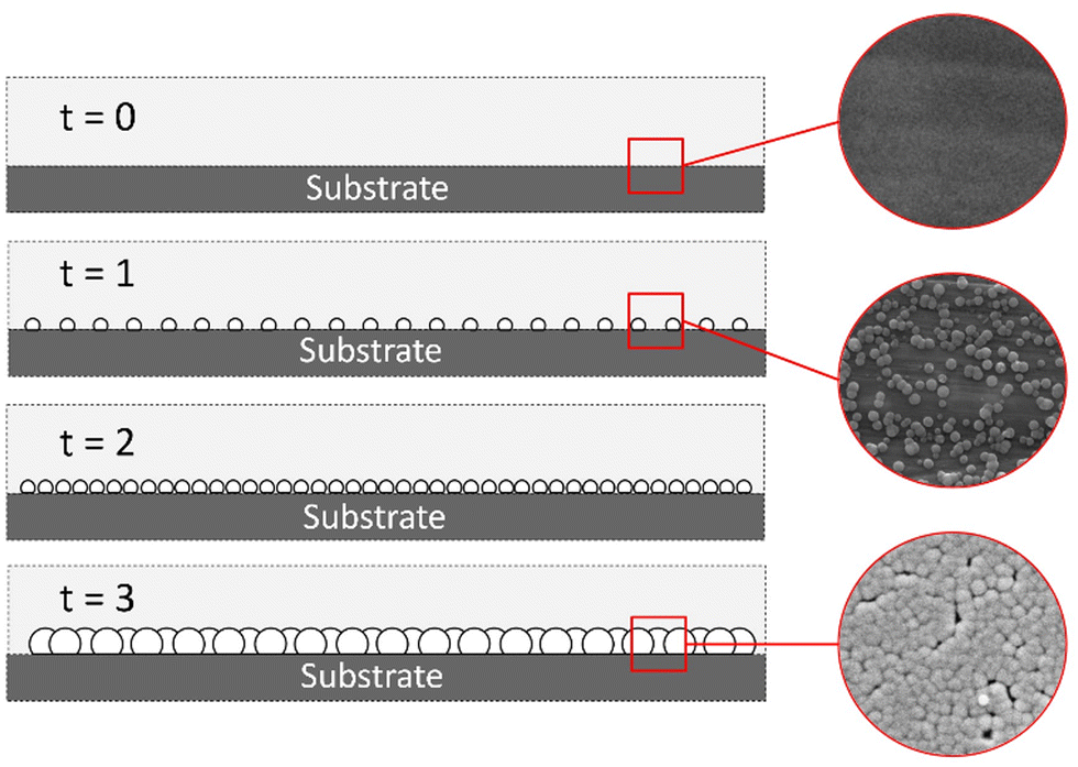
Heterogeneous nucleation.
The heterogeneous nucleation of Sb2S3 occurred in both zone 1 and zone 2. The heterogeneous nucleation on the substrate in zone 2 was the desired point of study since this was the patterned active material zone. Fig. 7 shows film formation due to heterogeneous nucleation on the substrate surface.
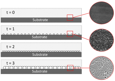 |
| | Fig. 7 Heterogeneous nucleation Sb2S3 film. | |
This heterogeneous nucleation behavior can be described by the total change in Gibbs free energy, as defined in eqn (5). The difference between heterogeneous and homogeneous nucleation is a wetting angle factor, which is always less than 1. γSM and γLM are the interfacial free energies between the solid-mold and liquid-mold. ASM is the area in contact between solid molds. Thus, as seen in eqn (6) and (7), the energetic barrier to heterogeneous nucleation is always less than the homogenous barrier to nucleation.
| | | ΔG(r) = VnucleiΔGV + AnucleiγSL + ASM (γSM − γLM) | (5) |
| | | ΔG(r) = ((4/3)πr3ΔGV + 4πr2γSL)S(θ) | (6) |
| | S(θ) = (2 + cos![[thin space (1/6-em)]](https://www.rsc.org/images/entities/char_2009.gif) θ)(1 − cosθ)2/4 θ)(1 − cosθ)2/4 | (7) |
| | | r* = −2γSL/ΔGV = −2γSLTm/ΔHfΔT | (8) |
| | | ΔG* = S(θ)(16πγ3SL/3ΔGV2) | (9) |
As previously described, the typical method flowed the reactants through a 3-meter long 35 °C water bath before flowing through the substrate reactor. The color of the reaction solution rapidly changed from clear precursors to white precipitate at the beginning of the bath and then to an orange-red color on the inlet of the substrate reactor. When the solution reached the waste storage, the color was dark orange-red. The reactor temperature was maintained at 80 °C for the deposition times ranging from 5–120 min. The resulting thin films were orange-red with a metallic shine.
Temperature vs. deposition rate
The growth rate was measured as a function of the glass substrate temperature. Stylus profilometry was used to measure the thickness and known time variable. The results (Fig. 8) show that as the substrate temperature increases, the growth rate increases. At low temperatures, this behavior is limited by kinetics; however, at high temperatures, this relationship is limited by the solvent boiling point. 2-Propanol was the limiting solvent and boils at 83 °C.
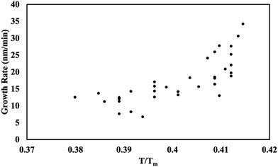 |
| | Fig. 8 Growth rate as a function of temperature on glass substrates. | |
Time vs. thickness barriers
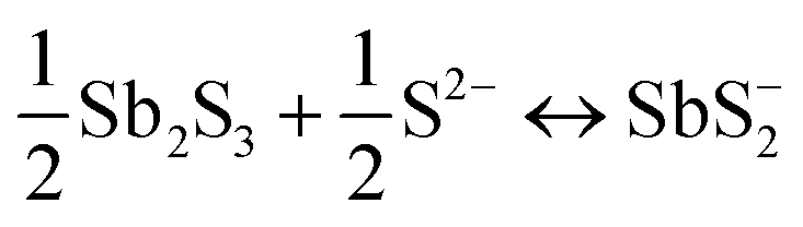
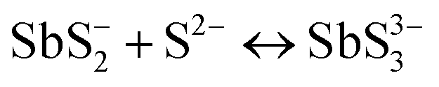
A key issue in all existing Sb2S3 methods was the growth-limiting parallel reaction of sulfur ions (S2−) dissolving the heterogeneously nucleated film in batch deposition methods by forming thioantimonate complexes as shown in eqn (10) and (11).38 Since MASL is a steady-state continuous flow method, this is theoretically mitigated, and the results validate this. The final resulting film thickness is plotted as a function of deposition time, with the MASL data compared against the chemical bath deposition method. All experiments in Fig. 9 were at 2.5 mL min−1, Tbath = 35 °C, Tsub = 80 °C, and deposited on clean glass slides. The literature data shows that the chemical bath deposition of the films peaks at about 2.5 μm (ref. 39) before dissolving. In contrast, the MASL method was carried out for 120 min and demonstrated continued thicknesses into 6.0 μm. The accumulation of sulfide ions due to the dissociation of the thiosulphate parallel to the growth of Sb2S3 explains the decrease in film thickness over time when used in CBD or any batch synthesis and deposition method. This factor means thicker films of Sb2S3 NPs are only possible in batch methods if the bath is repeatedly swapped out to eliminate the sulfide ions. However, this necessary step is impractical for commercial applications and corresponds to a non-steady state concentration of S2− ions. MASL eliminates the buildup of sulfide ions in the reaction since the process is a continuous flow method. This implies MASL can theoretically create thicker films than CBD since the concentration of sulfide ions at the deposition phase is steady state and does not accumulate and increase at the deposition site over the reaction time. This process advantage is required for thicker film applications in battery anodes and cathodes, as well as solar cells.| |  | (10) |
| |  | (11) |
 |
| | Fig. 9 Thickness vs. time comparison of MASL (this study) and chemical bath deposition.39 | |
Crystal structure and optical properties
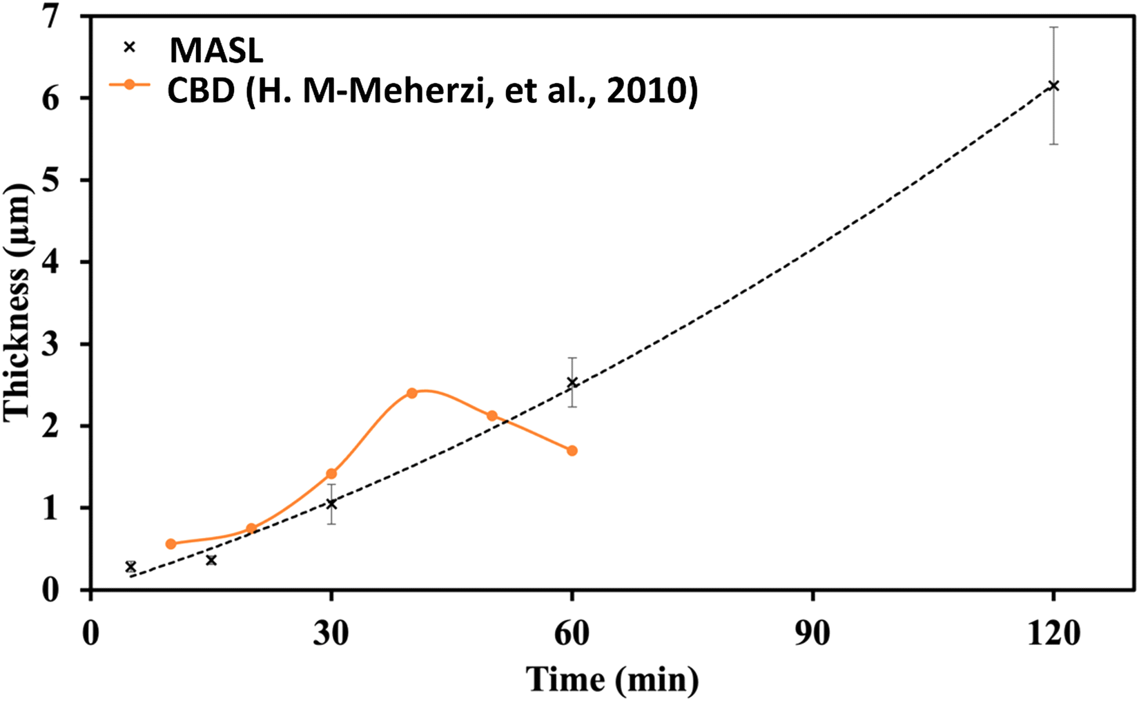
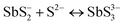
Rigaku SmartLab was used to perform X-ray diffraction on the samples at a scan rate of 0.05 deg s−1 with a Cu Kα source. The as-deposited thin films were amorphous and had no peaks. The XRD results shown in Fig. 10 are from a glass substrate sample deposited at a temperature of 80 °C, flow rate of 2.5 mL min−1, and deposition time of 15 minutes. The sample was annealed at 300 °C for 60 min in N2. All the XRD data was processed in GSAS 2 using reference.cif files from the Crystallography Open database.40,41 The oxide peaks observed are likely due to oxidation post-annealing (color change of the film was also noticed). The annealed samples show intensity peaks overlapping with the expected hkl planes for orthorhombic Sb2S3, as Bayliss, Nowacki, and Hoffman first reported.
 |
| | Fig. 10 XRD scan of annealed Sb2S3 thin films at 300 °C for 60 min on glass substrate. GSAS 2 refined XRD data (left); photo image of annealed sample (right). | |
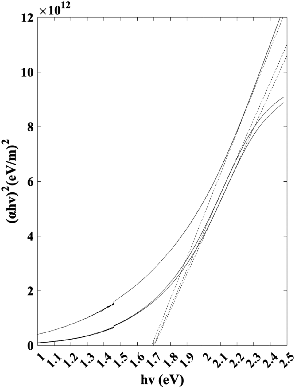
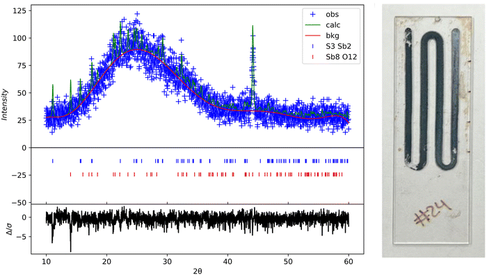
Jasco V-670 UV-vis/NIR spectrophotometer was used to characterize the band gap of the thin film samples. Scans were conducted between 300 nm and 800 nm. The Tauc plot used to identify the band gap is visualized in Fig. 11. Based on the linear extrapolations, the results indicate an average as-deposited Sb2S3 band gap of 1.7 eV. The band gap value is within the range of the reported values in the literature.42–44
 |
| | Fig. 11 Tauc plot for band gap calculation. | |
Growth and morphology of Sb2S3 on current collectors
Aluminum substrate coin cells.
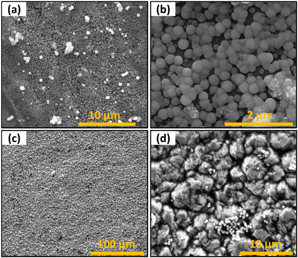
The coin cell samples were also imaged to observe the morphology of the active material in the device. The aluminum substrates resulted in highly uniform and narrow particle size distribution growth, as seen in Fig. 12a and b. Based on the SEM images, the average diameter of the spherical nanostructures was 235 nm (Fig. S5a, ESI†) for a substrate at 80 °C with a deposition time of 30 min. The EDS spectrum (Fig. S5a, ESI†) indicates an atomic ratio of Sb and S of about 1:2. As seen in Fig. 12b, heterogeneous nucleation of the spherical Sb2S3 occurred uniformly over the native surface roughness. These cells are not tested in the current work as Al current collectors are not used in LIB since Al alloys/de-alloys with Li at around ∼0.2 V vs. Li/Li+ and ∼0.6 V vs. Li/Li +, respectively.45 However, the results demonstrated direct growth of electrolytes on the Al current collectors and could be used in Na ion batteries in the future.46
 |
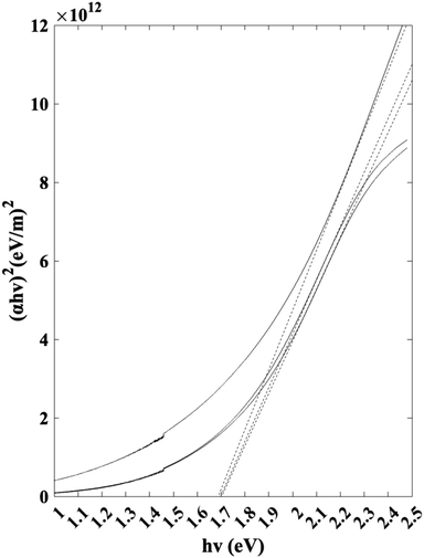
| | Fig. 12 SEM images of films deposited on current collector substrates (a) Sb2S3 on Al substrate (b) higher magnification of Sb2S3 on Al substrate (c) Sb2S3 on Cu substrate (d) higher magnification of Sb2S3 on Cu substrate. | |
Copper substrate coin cells.
Fig. 12c and d shows that the copper substrate samples showed only homogeneously nucleated particles deposited on the rough surface. This result suggested that heterogeneous nucleation was not occurring as expected and was likely due to an increased energy barrier caused by the native CuO layer, which was not removed during the cleaning process. However, the homogenously nucleated and deposited particles are Sb2S3 with an average diameter of 337 nm, and the EDS spectrum indicates the atomic ratio of Sb and S to be about 1:3 (Fig. S5b, ESI†). In this case, the excess sulfur is attributed to the formation of CuS since the Na2S2O3 can react with the copper.47
A different sample was prepared to test this nucleation barrier theory by removing the native CuO using dilute HCl. Furthermore, the polished side was used instead of the previous rough side (Fig. 13a and b). A rough surface has a lower energy barrier than a polished surface due to a lower nuclei volume and solid–liquid interface area achievable in rough crevasses. This concept is visualized in Fig. 13c and d and eqn (5).
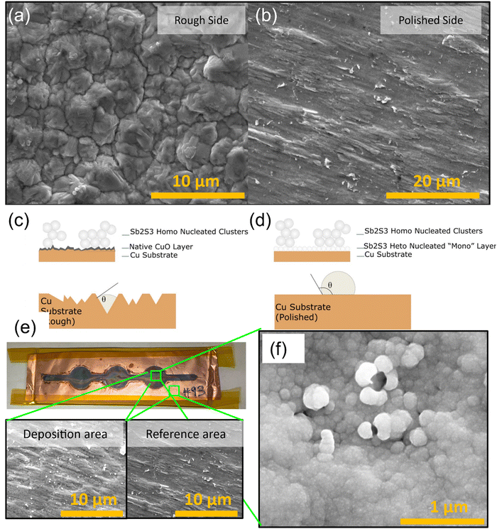 |
| | Fig. 13 SEM images of uncoated MTI Cu foil and nucleation barrier theory diagrams. (a) Rough side, (b) polished side, (c) native oxide barrier to heterogenous nucleation, (d) removed native oxide nucleation, (e) optical image of the deposited film on polished and cleaned Cu foil and SEM images of deposited and non-deposited areas, (f) Sb2S3 film deposited on polished copper foil substrates followed by HCl cleaning. | |
The results from this pure Cu and polished surface indicate successful heterogeneous nucleation, as seen in Fig. 13e and f. This confirms the theory that the native CuO layer sufficiently increased the energy barrier and prevented heterogeneous nucleation from occurring previously. As seen in Fig. 13d, the pure Cu substrate sample has highly uniform heterogeneous nucleation of the Sb2S3 and grain growth.
Cyclic voltammetry and galvanostatic charge–discharge cycling
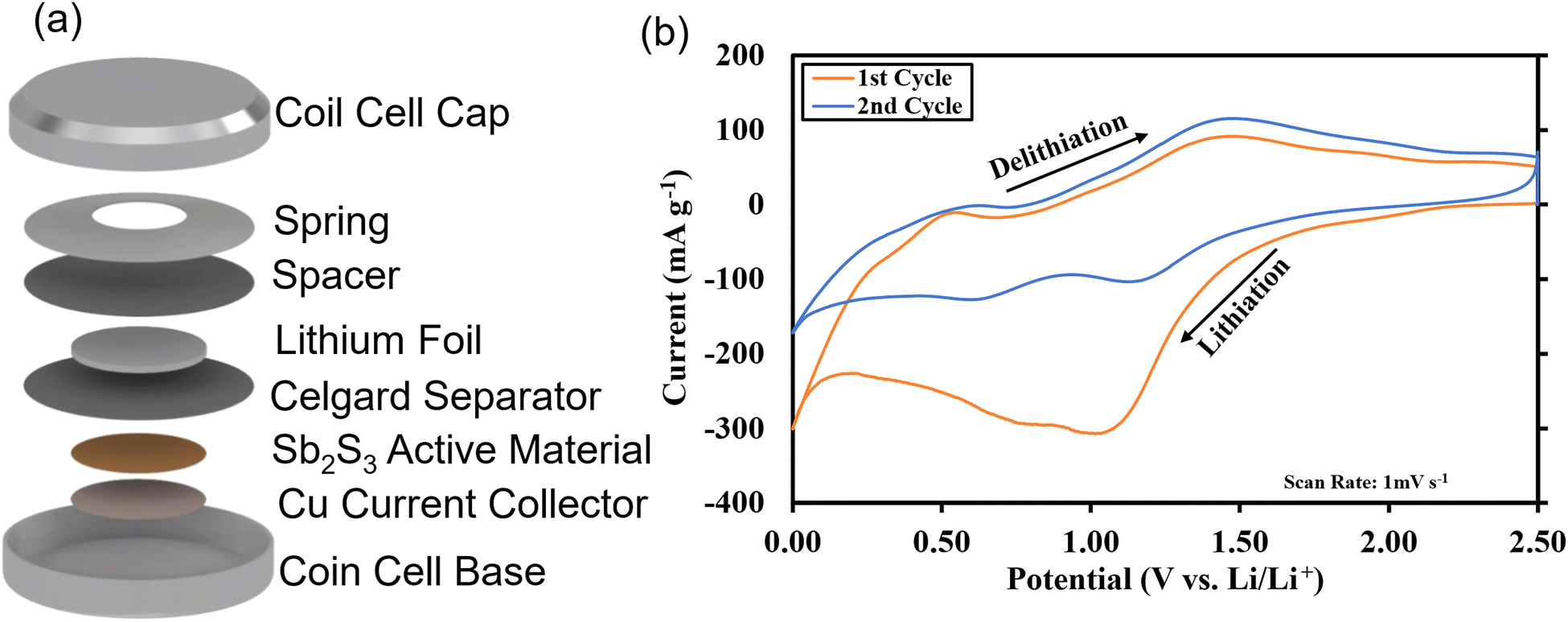
As-deposited Sb2S3 cyclic voltammetry.
Sb2S3 deposited anodes with 100% active material were used as working electrodes in Li-half cells. The half cells consist of a 1 cm diameter working electrode, Li metal counter electrode, CelgardTM separator, and 1 M LiPF6 (EC/DEC = 50/509 v/v) electrolyte as seen in Fig. 14a. No additional conductive additives or binders were used. The CV curves of the first and second cycles are shown in Fig. 14b. A scan rate of 1 mV s−1 was used between 0 and 2.5 V vs. Li+/Li. Both first and second-cycle curves have observable reduction and oxidation peaks, as similarly observed in the literature.4,48 During the cathodic scan (lithiation), the broad peaks at about 0.6 V and 1.15 V are attributed to the reduction of Sb2S3 (eqn (12)), While in the anodic scan (delithiation), the peaks at about 0.6 V and 1.5 V are attributed to the oxidation reaction. These results are typical of the conversion and alloying process presented in eqn (12)–(14).48| | 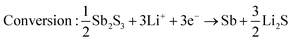 | (12) |
| | 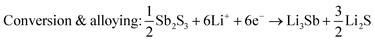 | (13) |
| | | Alloying: 6Li+ + 2Sb + 6e− → 2Li3Sb | (14) |
 |
| | Fig. 14 Coin cell prototype schematic. (a) CAD model breakdown; (b) 1st and 2nd cycle cyclic voltammetry curves. | |
As-deposited Sb2S3 in Li half-cell with Cu current collector GCD.
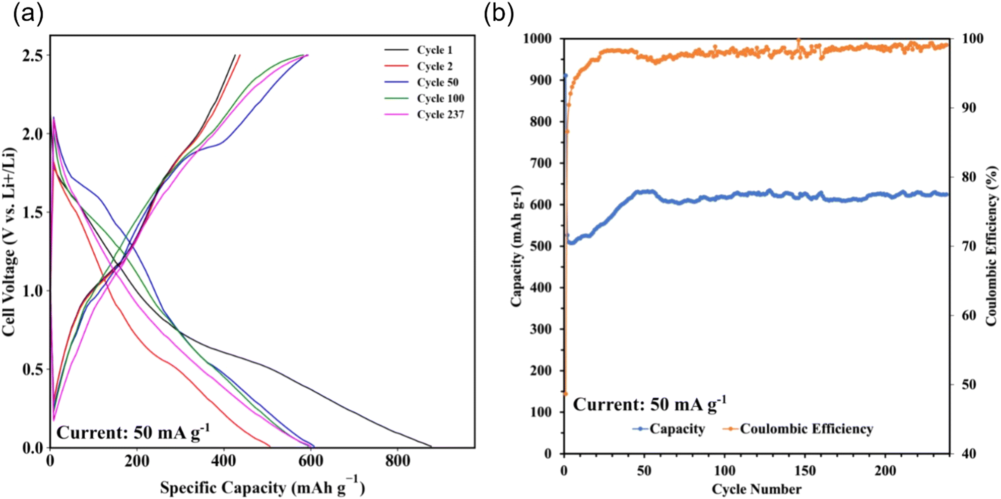
Sb2S3 thin films were grown on polished and HCl-cleaned MTI Cu foil substrates for 15 min at a flow rate of 2.5 mL min−1 with a Tsub = 80 °C and Tbath = 35 °C were used for this study. The electrode was a 500 nm Sb2S3 layer on a Cu current collector. The electrode composition was 100% active material and did not require a binder or conductive additive. The half cells were cycled at a current density of 50 mAg−1. The data indicates a first cycle capacity of ca. 900 mA h g−1 before dropping to a lower stable value. Fig. 15a shows the conversion and alloying reactions occurring between 1.7–1.2 V and 0.4–1 V, respectively. A stable capacity of ca. 600 mA h g−1 was observed for the first 237 cycles with a coulombic efficiency of 97–99% (Fig. 15b). This value is less than the theoretical maximum of 946 mA h g−1. However, the work demonstrates the MASL method's capability to directly synthesize and pattern functional battery anodes without additional steps or dangerous cleaning agents, which could supplement the rise of solid-state separator batteries. While likely incompatible with lithium–metal batteries at this stage, this work demonstrates an effective and highly controllable method for active material deposition and development.
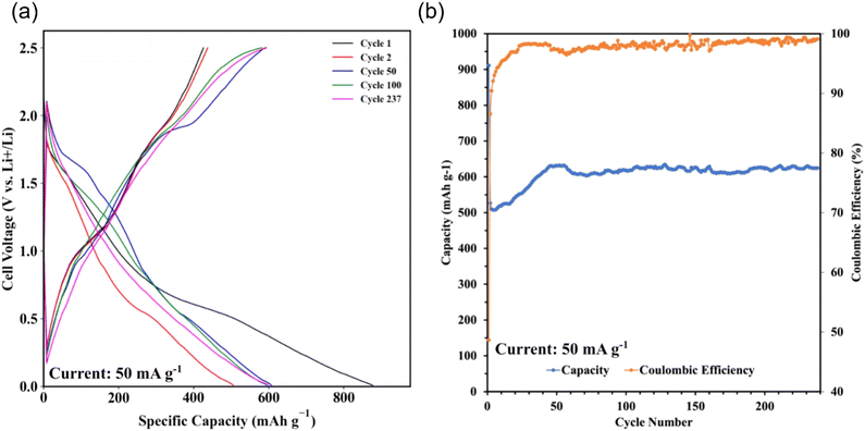 |
| | Fig. 15 GCD results. (a) Specific capacity vs. cell voltage; (b) coulombic efficiency and discharge capacity vs. cycle number. | |
Moreover, unlike previously reported colloidal synthesis methods, no conductive additive or binder was added to the sample for functional electrical performance. This is due to the fact that the Sb2S3 is directly nucleating, interfacing, and growing on the current collector rather than being physically packed like in the findings reported by Kravchyk et al.4 These findings demonstrate the electrochemical functionality of the Sb2S3 thin films via the MASL method. The calculated mass loading was about 0.164 mg cm−2.
Other ongoing research in emerging energy storage technologies has noted relevant challenges with multiphase material reactions.49–51 In particular, there is a growing focus on heterostructure materials that enable improved electrochemical performance while suppressing side reactions that traditionally degrade the active material. The growth of multi-layer complex materials demonstrates the need to progress toward steady-state process conditions. These challenges present areas of opportunity to further explore and integrate the MASL deposition method to manufacture complex battery materials.
Conclusions
The results demonstrate successful patterning and electrochemical cell functionality of Sb2S3 on glass, aluminum, and copper substrates via a microreactor-assisted nanomaterial deposition and soft lithography process at low temperatures between 10–80 °C. The resulting films are composed of spherical particle size with narrow distribution and have a bandgap of 1.7 eV. This newly deployed MASL method relies on a continuous flow microreactor design to achieve steady state reaction and nucleation conditions that enable highly programmable particle size outcomes. Both heterogenous and homogenous nucleation occurs, with most resulting film being heterogenous nucleated particles. Multiple experiments identified that the substrate's native oxide layer plays a significant role in the nucleation of Sb2S3 on copper substrates, increasing the interfacial free energy and barrier to nucleation. Thus, this oxide layer should be removed using dilute HCl. Furthermore, the results demonstrate mitigation of the time-dependent concentration of sulfur ions, which traditionally increase batch methods over reaction time and dissolve the Sb2S3 nucleated thin films. Furthermore, the electrochemical performance demonstrates functional Sb2S3 working electrodes without needing post-treatment, cleaning, or additional conductive or binding additives. Li half-cells showed a stable capacity of 600 mA h g−1 at 237 cycles and a coulombic efficiency of 97–99%. As the demand for higher-performing batteries increases, one route to achieve longer cycling batteries is to reduce the particle size of the active material in the anodes. Exploiting undercooling during synthesis and deposition may be beneficial, and the benefits come down to further particle size control and reduction. In particular, further exploration of achievable nano-geometries with undercooling may further expand material capabilities and electrode morphologies that could enable reduced cycle degradation. Other future work may also include the comparison of particle stability with undercooled nucleated anodes vs. more traditional batch methods like hot injection and capping. In conclusion, the MASL method offers a new way to enable tight control and deploy nanomaterials directly to the battery application surface without needing additional processing to achieve electrochemical functionality.
Data availability
The data supporting this article have been included as part of the ESI.†
Conflicts of interest
The authors declare that there are no conflicts of interest.
Acknowledgements
This work was supported by the U.S. National Science Foundation [CMMI# 1537196, CBET# 1449383, CMMI# 2001081, ECC# 1542101, PFI-RP 1941262, CBET#1949870, CBET#2016192, NNCI-2025489], Oregon Metal Initiative, and the Walmart Manufacturing Innovation Foundation.
References
- Z. Yuan, Z. Zeng, W. Zhao, Y. Dong, H. Lei, B. Wang, Y. Yang, W. Sun and P. Ge, ACS Appl. Energy Mater., 2023, 6, 12139–12165 CrossRef CAS.
- S. Barthwal, R. Kumar and S. Pathak, ACS Appl. Energy Mater., 2022, 5, 6545–6585 CrossRef CAS.
- U. Wijesinghe, G. Longo and O. S. Hutter, Energy Adv., 2023, 2, 12–33 RSC.
- K. V. Kravchyk, M. V. Kovalenko and M. I. Bodnarchuk, Sci. Rep., 2020, 10, 2554 CrossRef CAS PubMed.
- J. Zheng, C. Liu, L. Zhang, Y. Chen, F. Bao, J. Liu, H. Zhu, K. Shen and Y. Mai, Chem. Eng. J., 2022, 446, 136474 CrossRef CAS.
- S. S. Harke, T. Zhang, R. Huang and C. Gurnani, Mater. Adv., 2023, 4, 4119–4128 RSC.
- M. P. Motaung, D. C. Onwudiwe and W. Lei, ACS Omega, 2021, 6, 18975–18987 CrossRef CAS PubMed.
- Y. Dong, M. Hu, Z. Zhang, J. A. Zapien, X. Wang, J.-M. Lee and W. Zhang, ACS Appl. Nano Mater., 2019, 2, 1457–1465 CrossRef CAS.
- W. Lian, C. Jiang, Y. Yin, R. Tang, G. Li, L. Zhang, B. Che and T. Chen, Nat. Commun., 2021, 12, 3260 CrossRef CAS PubMed.
- K. Ye, B. Wang, A. Nie, K. Zhai, F. Wen, C. Mu, Z. Zhao, J. Xiang, Y. Tian and Z. Liu, J. Mater. Sci. Technol., 2021, 75, 14–20 CrossRef CAS.
- Y. Zeng, K. Sun, J. Huang, M. P. Nielsen, F. Ji, C. Sha, S. Yuan, X. Zhang, C. Yan, X. Liu, H. Deng, Y. Lai, J. Seidel, N. Ekins-Daukes, F. Liu, H. Song, M. Green and X. Hao, ACS Appl. Mater. Interfaces, 2020, 12, 22825–22834 CrossRef CAS PubMed.
- D. Santos-Cruz, M. de la L. Olvera-Amador, S. A. Mayen-Hernandez, J. G. Quiñones-Galván, J. Santos-Cruz and F. de Moure-Flores, J. Laser Appl., 2021, 33, 42012 CrossRef CAS.
- M. M. Gomaa, M. H. Sayed, M. S. Abdel-Wahed and M. Boshta, RSC Adv., 2023, 13, 22054–22060 RSC.
- S. Shaji, L. V. Garcia, S. L. Loredo, B. Krishnan, J. A. Aguilar Martinez, T. K. Das Roy and D. A. Avellaneda, Appl. Surf. Sci., 2017, 393, 369–376 CrossRef CAS.
- P. Vadhva, T. E. Gill, J. H. Cruddos, S. Said, M. Siniscalchi, S. Narayanan, M. Pasta, T. S. Miller and A. J. E. Rettie, Chem. Mater., 2023, 35, 1168–1176 CrossRef CAS PubMed.
- S. Iwasaki, T. Hamanaka, T. Yamakawa, W. C. West, K. Yamamoto, M. Motoyama, T. Hirayama and Y. Iriyama, J. Power Sources, 2014, 272, 1086–1090 CrossRef CAS.
- H. Maghraoui-Meherzi, T. Ben Nasr, N. Kamoun and M. Dachraoui, Phys. B, 2010, 405, 3101–3105 CrossRef CAS.
- P. Nair, Sol. Energy Mater. Sol. Cells, 1998, 52, 313–344 CrossRef CAS.
- N. Bouaniza, N. Hosni and H. Maghraoui-Meherzi, Surf. Coat. Technol., 2018, 333, 195–200 CrossRef CAS.
- C. H. Chang, B. K. Paul, V. T. Remcho, S. Atre and J. E. Hutchison, J. Nanopart. Res., 2008, 10, 965–980 CrossRef CAS.
- V. V. K. Doddapaneni, J. A. Dhas, A. Chang, C. Choi, S. Han, B. K. Paul and C. Chang, MRS Energy Sustainability, 2022, 9, 407–442 CrossRef.
- Y.-W. Su, S. Ramprasad, S.-Y. Han, W. Wang, S.-O. Ryu, D. R. Palo, B. K. Paul and C. Chang, Thin Solid Films, 2013, 532, 16–21 CrossRef CAS.
- S. Ramprasad, Y.-W. Su, C.-H. Chang, B. K. Paul and D. R. Palo, ECS J. Solid State Sci. Technol., 2013, 2, P333–P337 CrossRef CAS.
- P. Vas-Umnuay, K.-J. Kim, D.-H. Kim and C.-H. Chang, CrystEngComm, 2015, 17, 2827–2836 RSC.
- C.-H. Choi and C. Chang, Cryst. Growth Des., 2014, 14, 4759–4767 CrossRef CAS.
- S.-Y. Han, B. K. Paul and C. Chang, J. Mater. Chem., 2012, 22, 22906 RSC.
- C.-H. Choi, B. Paul and C.-H. Chang, Processes, 2014, 2, 441–465 CrossRef.
- V. V. K. Doddapaneni, A. Chang, H.-Y. Jun, C.-H. Choi, Z. Feng and C. Chang, CrystEngComm, 2023, 25, 5606–5628 RSC.
- Z. Gao, V. V. K. Doddapaneni, C. Pan, R. Malhotra and C. Chang, Adv. Eng. Mater., 2024, 240112 Search PubMed.
- M. Kim, S. K. Kang, J. Choi, H. Ahn, J. Ji, S. H. Lee and W. B. Kim, Nano Lett., 2022, 22, 10232–10239 CrossRef CAS PubMed.
- C. Lee, S. S. Shin, J. Choi, J. Kim, J.-W. Son, M. Choi and H. H. Shin, J. Mater. Chem. A, 2020, 8, 16534–16541 RSC.
- I. Kokal, O. F. Göbel, E. J. van den Ham, J. E. ten Elshof, P. H. L. Notten and H. T. Hintzen, Ceram. Int., 2015, 41, 13147–13152 CrossRef CAS.
- C. Karuppiah, S. L. Beshahwured, Y.-S. Wu, L. M. Babulal, K. Z. Walle, H. K. Tran, S.-H. Wu, R. Jose and C.-C. Yang, ACS Appl. Energy Mater., 2021, 4, 11248–11257 CrossRef CAS.
- Q. Kang, Z. Zhuang, Y. Liu, Z. Liu, Y. Li, B. Sun, F. Pei, H. Zhu, H. Li, P. Li, Y. Lin, K. Shi, Y. Zhu, J. Chen, C. Shi, Y. Zhao, P. Jiang, Y. Xia, D. Wang and X. Huang, Adv. Mater., 2023, 35, 2303460 CrossRef CAS PubMed.
- J. Kim, Z. Li and I. Park, Lab Chip, 2011, 11, 1946 RSC.
- F. Tian, L. Cai, C. Liu and J. Sun, Lab Chip, 2022, 22, 512–529 RSC.
-
T. Schneller, R. Waser, M. Kosec and D. Payne, Chemical Solution Deposition of Functional Oxide Thin Films, Springer, Vienna, Vienna, 2013 Search PubMed.
- M. T. S. Nair, Y. Peña, J. Campos, V. M. García and P. K. Nair, J. Electrochem. Soc., 1998, 145, 2113–2120 CrossRef CAS.
- H. Maghraoui-Meherzi, T. Ben Nasr, N. Kamoun and M. Dachraoui, C. R. Chim., 2010, 14, 471–475 CrossRef.
- P. Bayliss and W. Nowacki, Z. Kristallogr. - Cryst. Mater., 1972, 135, 308–315 CrossRef CAS.
- W. Hofmann, Z. Kristallogr. - Cryst. Mater., 1933, 86, 225–245 CrossRef CAS.
- S.-J. Lee, S.-J. Sung, K.-J. Yang, J.-K. Kang, J. Y. Kim, Y. S. Do and D.-H. Kim, ACS Appl. Energy Mater., 2020, 3, 12644–12651 CrossRef CAS.
- J. Zhou, J. Chen, M. Tang, Y. Liu, X. Liu and H. Wang, RSC Adv., 2018, 8, 18451–18455 RSC.
- L. Guo, B. Zhang, S. Li, Q. Zhang, M. Buettner, L. Li, X. Qian and F. Yan, APL Mater., 2019, 7, 41105 CrossRef.
- X. Zhang, Y. Tang, F. Zhang and C.-S. Lee, Adv. Energy Mater., 2016, 6, 1502588 CrossRef.
- T.-E. Fan and H.-F. Xie, J. Alloys Compd., 2019, 775, 549–553 CrossRef CAS.
- A. R. Al Rashed, F. M. Al Kharafi, B. G. Ateya and I. M. Ghayad, Egypt. J. Chem., 2014, 57, 109–127 CrossRef.
- D. Y. W. Yu, H. E. Hoster and S. K. Batabyal, Sci. Rep., 2014, 4, 4562 CrossRef PubMed.
- S. Wang, W. Jiang, J. Wu, H. Huang, P. Guo, X. Zhang, H. Gu, Q. Huang and Y. Hu, Energy Adv., 2022, 1, 704–714 RSC.
- J. Xie, F. Cheng, R. Chen, Z. Jin and L. Sun, J. Mater. Chem. A, 2024, 12, 10737–10744 RSC.
- L. Sun, Y. Liu, J. Xie, L. Fan, J. Wu, R. Jiang and Z. Jin, Chem. Eng. J., 2023, 451, 138370 CrossRef CAS.
|
| This journal is © The Royal Society of Chemistry 2024 |
Click here to see how this site uses Cookies. View our privacy policy here. 
 Open Access Article
 This Open Access Article is licensed under a Creative Commons Attribution-Non Commercial 3.0 Unported Licence
 b,
Marcos
Lucero
b,
Changqing
Pan
b,
Marcos
Lucero
b,
Changqing
Pan