
 Open Access Article
 This Open Access Article is licensed under a Creative Commons Attribution-Non Commercial 3.0 Unported Licence
Current trends and emerging opportunities for 2D materials in flexible and wearable sensors
Nongthombam Joychandra
Singh
 ,
Isha
Basumatary
,
Chandra Sekhar Reddy
Kolli
and
Parikshit
Sahatiya
*
,
Isha
Basumatary
,
Chandra Sekhar Reddy
Kolli
and
Parikshit
Sahatiya
*
Department of Electrical and Electronics Engineering, Birla Institute of Technology and Science Pilani Hyderabad Campus, Hyderabad 500078, India. E-mail: parikshit@hyderbad.bits-pilani.ac.in
First published on 17th June 2025
Abstract
The emergence of two-dimensional (2D) materials has dramatically transformed the landscape of modern electronics, particularly in the realm of wearable, flexible, and next-generation devices. This feature article summarises our achievements and the potential of 2D materials in developing wearable device prototypes, highlighting key material properties, device architectures, and fabrication strategies for innovative applications in healthcare monitoring, multimodal sensing, neuromorphic sensing, human–machine interfaces, and environmental sensing. Emphasis is placed on understanding the interplay between material characteristics and sensor performance, including sensitivity, stability, and biocompatibility. Additionally, challenges such as scalability, integration with flexible substrates, and long-term reliability are discussed, alongside potential solutions and future directions. This article presents an in-depth review of the recent progress in the emerging 2D materials with potential to facilitate future breakthroughs in flexible and wearable sensing technologies.
1. Introduction
The continuous evolution of wearable and flexible sensors has significantly transformed the field of modern electronics, paving the way for new applications in areas such as healthcare monitoring, robotics, human–machine interfaces, and environmental sensing. A major contributing factor to this innovation is the advancements in 2D materials, including graphene,1 black phosphorus,2 TMDs,3 and MXenes,4 which are widely explored material platforms for technological study and advancement of atomic-level applications. These 2D materials are notable for their remarkable properties, such as a high surface-to-volume ratio, mechanical flexibility, outstanding electrical and thermal conductivity, and atomic-scale thickness. These remarkable attributes make 2D materials ideal for application in cutting-edge sensor technologies. Among the family of 2D materials, TMDs are some of the most widely studied materials, particularly for sensing, biosensing, optoelectronic and energy storage applications. These layered materials feature metal atoms sandwiched between the layers of chalcogen atoms. The general formula for TMDs is MX2, where M denotes a transition metal (such as Mo, W, Ti, or Nb), and X signifies a chalcogen (such as S, Se, or Te). The metal atoms (M) are covalently bonded to the neighbouring chalcogens (X).5 These layers are held together in a stack via weak van der Waals forces of attraction. TMDs exist in three polytypes that are distinguished by their crystal structures: 2H, 3R, and 1T.6 The letters H, R, and T refer to hexagonal, rhombohedral, and trigonal crystal structures, respectively. Among them, the 2H structure is the most thermodynamically stable and exhibits semiconducting properties, while the 1T structure is metastable and displays metallic properties.A noteworthy family of emerging 2D materials is MXenes, which have the general formula Mn+1XnTx and are composed of transition metal carbides, nitrides, or carbonitrides. These materials are recognized for their distinct layered metallic structure and intriguing properties such as high electrical conductivity, similar to metals’; enhanced ionic conductivity; and hydrophilic characteristics originating from the presence of functional groups (–OH, –O, and –F) on their surfaces.7–9 Additionally, MXenes are mechanically flexible; through adjustable etching techniques, it is possible to control the morphology of MXenes to create nanoparticles or single and multi-layered nanosheets, which feature large specific surface areas, boosting their sensing capabilities. Moreover, MXenes can be easily integrated with other materials to form composites. By tailoring their structure, MXenes and their composites can achieve improved mechanical flexibility and stretchability, making them suitable for various applications in wearable technologies, such as flexible physical and chemical sensors.10 The fabrication technologies for integrating 2D materials into wearable sensors are diverse ranging from mechanical exfoliation and chemical vapour deposition (CVD) to solution-based methods such as spin coating and inkjet printing.11 These techniques allow the production of high-quality 2D material films on flexible substrates, such as polymers, textiles, and even paper. Advanced lithographic processes have further facilitated the creation of miniaturized and high-performance sensor arrays, enhancing the scalability and practicality of these devices for mass-market adoption.12
In this feature article, we present the developments of flexible and wearable sensors for physical and chemical sensing utilizing 2D materials. Discussions highlighting key material properties, device architectures, and fabrication strategies are presented. Emphasis is placed on understanding the interplay between material characteristics and sensor performance, including sensitivity, stability, and biocompatibility. Different sensing mechanisms are explained utilizing percolation networks and band structures. Applications including human–machine interactions, consumer electronic applications, and gaming are discussed, with an emphasis on our contribution to this field. Further, state-of-the-art applications, including electronic skin, and multimodality in sensor computing, are discussed, and the importance of 2D materials in this context is explained. Finally, the challenges in the field of 2D material-based flexible and wearable sensors are presented, together with our perspectives in this field for the next decade, including a discussion on the open-ended questions in this field (Fig. 1 and 2).
 | ||
| Fig. 1 Timeline of different materials in the development of flexible sensors. | ||
 | ||
| Fig. 2 Evolution of the development technology trends for 2D materials and their implementation in various flexible and wearable device applications. (Bottom right) Reproduced from ref. 13 Copyright Letter Nano, reproduced from ref. 14 Copyright the American Chemical Society, reproduced from ref. 15 Copyright Springer Nature, Imperceptible electronic foil,16 reproduced from ref. 17 Copyright the American Chemical Society, CVD grown graphene e-skin,18 reproduced from ref. 19 Copyright the American Chemical Society, reproduced from ref. 20 Copyright Springer Nature, reproduced from ref. 21 Copyright the American Chemical Society, reproduced from ref. 22 Copyright from American Chemical Society, reproduced from ref. 23 Copyright from American Chemical Society, reproduced from ref. 25 Copyright from American Chemical Society, reproduced from ref. 24 Copyright Nature, reproduced from ref. 26 Copyright from Springer Nature, reproduced from ref. 27 Copyright from the American Chemical Society, reproduced from ref. 28 Copyright from Elsevier. | ||
2. Properties of 2D materials for flexible and wearable sensors
2.1 Mechanical properties of 2D materials
Two-dimensional materials possess mechanical properties, demonstrating extremely high in-plane stiffness and strength, while also being remarkably flexible due to their atomic thickness.29 This unique combination allows them to bend significantly without losing their structural integrity. The interactions between these materials and other layers or substrates are predominantly influenced by weak van der Waals forces, which play a role in their shear, friction, and fracture behaviour. Applications that are flexible, such as wearable sensors, flexible displays, and healthcare monitoring devices, rely on ultrathin electronic materials that deliver exceptional stretchability and mechanical flexibility for their intended purposes.30 The most remarkable characteristics of layered 2D materials are their mechanical flexibility and toughness, making them particularly attractive for flexible applications. However, because of the higher degree of stiffness and brittle characteristics of conventional semiconductors in their bulk form, they cannot satisfy the requirements for flexible electronics when operated under higher strain in devices fabricated using them.31 In contrast, owing to the outstanding features of 2D layered materials, including impressive mechanical flexibility and toughness, they are especially appealing for flexible applications.32 The Young's modulus and strain thresholds of different materials, including conductors such as graphene and semiconductors such as TMDs, MXenes, and BP, are utilised to produce flexible devices, as illustrated in Fig. 3. Graphene, a leading 2D material, consists of a single layer of carbon atoms arranged in a honeycomb structure. It demonstrates remarkable flexibility together with a high Young's modulus (∼1 TPa), low stiffness, and significant strain limit (∼25%), making it particularly well-suited for the fabrication of flexible biosensors that can be worn on human skin and implantable bioelectronic devices.33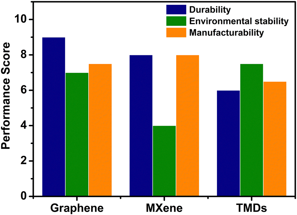 | ||
| Fig. 3 Performance score evaluation of graphene, TMDs and MXenes towards durability, environmental stability and manufacturability. | ||
In TMDs, the transition metal (Mo, W, V, Ti, etc.) layers are hexagonally close-packed and sandwiched between two layers of chalcogen atoms (S or Se).34 Most of the members of the TMD family with sandwich structures exhibit a Young's modulus in the range of 120–400 GPa with a breaking strain limit of 6–11%.35 Compared to MoS2, other TMDs such as MoSe2, WS2, and WSe2 exhibit similar mechanical properties due to their obvious structural similarities (E in the range of 154.5–291.2 GPa).36 Liu et al. synthesized monolayer MoS2 and WS2 through CVD and found a similar elastic modulus of approximately 170 N m−2 in both materials.37 This finding was almost identical to that of exfoliated MoS2 and 50% of the graphene module. BP is another auspicious 2D material with excellent mechanical features and promising electrical and optical properties. Monolayer BP (phosphorene) is organized as a puckered honeycomb structure in which phosphorus atoms are covalently bonded with three adjoining phosphorus atoms via sp3 hybridization.38 Due to this puckered structure, phosphorene exhibits Young's modulus in the range of 44 to 166 GPa (armchair to zigzag direction) and a fracture strain of 30% for monolayer and 32% for multilayer. Borophene is another member of the new generation of 2D layered materials, which exhibits a Young's modulus of 166 GPa and 389 GPa and fracture strain of 15% and 8% along the β- and α-directions, respectively.39 MXenes are another class of 2D transition metal nitrides and carbides represented by Mn+1AXn, where M represents an early transition metal; A is an A-group element such as Al and Si, X is carbon or nitrogen, and n is an integer of 1–3. Monolayer Ti3C2Tx MXene exhibits an effective elastic strain of 3.2% with a Young's modulus of 484 GPa.40
2.2 Electrical properties of 2D materials
The remarkable electrical properties of 2D materials drive their application in flexible and wearable electronics. The mobility of charge carriers is a specific intrinsic characteristic of materials, influenced by their chemical bonding, atomic size, atomic number, lattice strain, and crystal structure. A summary of the charge carrier mobilities of different 2D materials is presented in Fig. 3 (right). Single-element atomic sheets are low-bandgap materials among the diverse range of 2D materials with higher electronic mobility values. For instance, silicene exhibits the mobility of 2100 cm2 V−1 s−1, whereas graphene has been reported to possibly have the highest experimental value of 180![[thin space (1/6-em)]](https://www.rsc.org/images/entities/char_2009.gif) 000 cm2 V−1 s−1.41 Borophene is another elemental atomic sheet that possesses an anisotropic planar structure with corrugation and buckling along the α- and β-directions, which has been reported to exhibit a comparable charge carrier mobility to that of graphene (∼105 cm2 V−1 s−1).42 MXenes, a recently developed class of layered 2D transition metal carbides, display semiconducting properties with a tunable bandgap in the range of 0.24–1.8 eV. The electronic band structures of MXenes can be tuned by functionalizing their surface with different functional groups. For example, pure and F-functionalized Ti2C are metallic, whereas Ti2C exhibits semiconducting nature when functionalized with oxygen atoms. Similar to borophene, MXenes display anisotropic behaviour in their electrical and mechanical properties. For example, monolayers of Ti2CO2 MXene exhibit different hole mobilities of 7400 and 2250 cm2 V−1 s−1 along the x- and y-directions, respectively.43
000 cm2 V−1 s−1.41 Borophene is another elemental atomic sheet that possesses an anisotropic planar structure with corrugation and buckling along the α- and β-directions, which has been reported to exhibit a comparable charge carrier mobility to that of graphene (∼105 cm2 V−1 s−1).42 MXenes, a recently developed class of layered 2D transition metal carbides, display semiconducting properties with a tunable bandgap in the range of 0.24–1.8 eV. The electronic band structures of MXenes can be tuned by functionalizing their surface with different functional groups. For example, pure and F-functionalized Ti2C are metallic, whereas Ti2C exhibits semiconducting nature when functionalized with oxygen atoms. Similar to borophene, MXenes display anisotropic behaviour in their electrical and mechanical properties. For example, monolayers of Ti2CO2 MXene exhibit different hole mobilities of 7400 and 2250 cm2 V−1 s−1 along the x- and y-directions, respectively.43
MXenes are known for their excellent electronic conductivity, which can be improved by intercalating cations or organic molecules. Zhang et al. showed that some hydroxyl-terminated MXenes have nearly free electron states, featuring a bandgap of up to 0.194 eV. These states are situated outside the surface atoms and run parallel to the surface. It is recognized that bare MXene compounds, such as Tin+1Xn, display metallic characteristics. As the value of n increases, the formation of additional Ti–X bonds diminishes the strength of these metallic properties.44 Due to the presence of an additional electron in the nitrogen atom compared to the carbon atom, titanium nitrides exhibit greater metallic properties than titanium carbides in X atoms. Additionally, depending on the types and orientations of the surface groups, MXene sheets can function as either narrow-band-gap semiconductors or metals. Conversely, TMDs possess a semiconducting nature with mobility up to a few hundred cm2 V−1 s−1 at room temperature in their monolayer form. The extensive collection of transition metal dichalcogenides (TMDs) includes various materials with different bandgap values, offering a range of 2D materials for targeted applications. Moreover, the bandgap of TMDs can be significantly adjusted by reducing their thickness from bulk to a single layer. The band structure of layered TMDs is considerably influenced by the interplay of quantum confinement and interactions between layers. As the number of layers decreases, the effects of quantum confinement become more pronounced, while the strength of the interlayer interactions diminishes.45
These two effects not only affect the band gap value but also influence the direct and indirect nature of the band gap. In transition metal dichalcogenides (TMDs) such as MoS2, decreasing the number of layers leads to a gradual increase in the energy associated with the indirect excitonic transition, while the direct bandgap at the k point within the Brillouin zone remains relatively stable. Significantly, when MoS2 is reduced to a single layer, the energy of its indirect bandgap exceeds that of the direct transition, causing it to become a direct bandgap 2D semiconductor with an energy bandgap of around 1.9 eV.46 Likewise, other transition metal dichalcogenide (TMD) monolayers, including WS2 (approximately 2.1 eV), WSe2 (around 1.6 eV), MoSe2 (about 1.5 eV), MoTe2 (nearly 1.1 eV), and PtSe2 (approximately 1.8 eV), possess a direct band gap. In comparison, their bulk forms possess an indirect bandgap characteristic with lower values. Among the TMDs, the simple synthesis and extraordinary physical, physicochemical, and electronic properties of MoS2 make it the most promising material for flexible electronic applications.47 BP stands out as a notable layered semiconductor, offering a tunable direct bandgap from 2.0 in monolayer form to 0.3 eV in the bulk, together with a high carrier mobility of around ∼1000 cm2 V−1 s−1.38,48
2.3 Comparative analysis of 2D materials under practical constraints
Graphene is a 2D material recognised for its exceptional flexibility, transparency, and electrical conductivity, making it suitable for various advanced applications. Furthermore, its extensive surface area facilitates significant interactions with other materials, enhancing its overall utility. Nonetheless, graphene has certain drawbacks, notably the absence of a bandgap, which complicates its function in electronic devices due to the lack of selective sensing. The connection between its electrical performance and the intricacies of functionalization is complex, where improving its characteristics often necessitates advanced chemical modifications. However, despite these obstacles, graphene shows remarkable chemical stability and durability under stress, which are essential for applications requiring resilience. One effective method for the large-scale production of graphene is chemical vapor deposition (CVD), although the quality of the resulting graphene can vary greatly due to the use of different techniques and conditions, presenting challenges in its uniform manufacturing. Graphene shows potential for application in various areas, including strain sensors, touch screens, transparent electrodes, and gas or vapor sensors.18,49 Additionally, to enhance its capabilities, strategies such as doping and combining graphene with transition metal dichalcogenides (TMDs) or MXenes can be applied. These approaches aim to improve its performance in electronics and sensor technologies, expanding its applicability and efficacy.TMDs (transition metal dichalcogenides), such as MoS2 and WS2, are a distinct class of materials with fascinating properties suitable for a range of electronic and optoelectronic applications. A key feature of TMDs is their semiconducting bandgap, enabling their effective use in devices that necessitate controlled electrical conductivity. Alongside their electronic properties, TMDs display excellent mechanical characteristics, including flexibility and strength, as well as desirable optical features such as strong light absorption and photoluminescence. However, TMDs also have certain limitations, for example, their carrier mobility is lower than that of graphene, which may hinder their performance in high-speed electronic applications. Additionally, in single-layer form, these materials can be brittle and vulnerable to mechanical stress and fracture. TMDs feature tunable bandgaps, which can be adjusted based on their number of layers or exposure to external stimuli, facilitating a balance between conductivity and the desired electronic characteristics for particular applications. Nonetheless, this tunability underscores the necessity for protective coatings to mitigate mechanical stress, given that the durability of TMDs can be moderate in practical scenarios. TMDs can be fabricated through methods such as mechanical exfoliation and chemical vapor deposition (CVD); however, achieving large-area uniformity continues to be a challenge, limiting their scalability for commercial use. They have been applied in various devices, such as field-effect transistor (FET)-based sensors, photodetectors, and pressure and biosensors, where their unique electronic and optical traits can be effectively utilized.5,50–52 Moreover, TMDs are frequently combined with other materials such as graphene and MXenes to form heterostructures, which enhance their functionality and performance in advanced applications, establishing TMDs as a crucial element in developing next-generation electronic and optoelectronic devices.
MXenes, including Ti3C2Tx, are a captivating category of two-dimensional materials recognized for their outstanding properties. They exhibit very high electrical conductivity, making them suitable for various electronic applications. Furthermore, MXenes are hydrophilic and feature tunable surface terminations, which allow custom modifications to improve their interactions in diverse environments. However, these materials are prone to oxidation and moisture degradation, which can affect their long-term stability. Furthermore, although they possess high sensitivity in several applications, this sensitivity can compromise their durability, necessitating their encapsulation to shield them from humid conditions. Generally, the production of MXenes involves processes such as HF etching and delamination, which are moderately scalable and appropriate for industrial use. Given their distinct characteristics, the application of MXenes has been investigated in pressure, strain, and electrochemical biosensors, as well as in electromagnetic interference (EMI) shielding and wearable technology.53–55 Researchers are also exploring composite materials combining MXenes with polymers or graphene to create hybrid materials that harness the advantages of each component, improving their stability and flexibility.
Hexagonal boron nitride (h-BN) is another innovative material well-known for its exceptional properties. It is chemically inert, making it highly stable in various settings and suitable for applications that involve extreme temperatures or harsh chemical environments. Notably, h-BN has outstanding thermal conductivity and dielectric properties, effectively dissipating heat, while serving as an excellent electrical insulator. However, it lacks active sensing capabilities on its own; instead, it provides support in electronic systems, particularly in hybrid configurations. When paired with other two-dimensional materials such as graphene and molybdenum disulfide (MoS2), h-BN significantly boosts the performance of flexible electronics. Its high mechanical strength offers reliable support, enabling the creation of devices that are both durable and flexible. This dual functionality as an insulating substrate and structural support is crucial for developing next-generation electronic devices that need to be bendable or stretchable. However, despite its benefits, producing h-BN through chemical vapor deposition (CVD) can be expensive. Nevertheless, its excellent chemical and thermal stability make it a valuable investment for high-performance applications.56,57 Overall, h-BN is a key component in advanced electronic designs, particularly in flexible electronics, where it is employed for encapsulation, as a gate dielectric, and in synergy with active two-dimensional materials for hybrid applications.
Black phosphorus (BP) is a noteworthy material featuring a tunable direct bandgap and high electronic mobility, making it appealing for a variety of optoelectronic applications. However, a significant challenge associated with BP is its extreme sensitivity to environmental factors. It is very susceptible to air, leading to quick degradation when exposed to oxygen and moisture, which restricts its usability in open environments. This environmental instability is a considerable drawback of BP, despite its strong performance in photodetectors, gas sensors, and pressure sensors.58,59 Thus, to address these degradation concerns, encapsulation methods using materials such as aluminum oxide (Al2O3) and hexagonal boron nitride (h-BN) are commonly used to protect BP from detrimental external conditions. However, the synthesis of black phosphorus remains challenging, given that current methods primarily rely on exfoliation techniques, which are not easily scalable for mass production. Consequently, the research on BP and its development are still in their infancy, with ongoing efforts focused on improving its stability and broadening its potential applications. With the continuing advancements, there is optimism that these challenges will be overcome, allowing black phosphorus to realize its full potential in electronic and optoelectronic devices (Table 1).60
| 2D materials | Mechanical properties | Electrical properties | Ref. | ||
|---|---|---|---|---|---|
| Strain (%) | Young's modulus (GPa) | Band gap (eV) | Mobility (cm2 V−1 s−1) | ||
| Graphene | 25 | 1000 | 0 | 180000 |
44 |
| Borophene | 15 | 389 N m−1 | 0.4 | ∼105 | 39 |
| Black phosphorus | 30 | 44–166 | 0.3–2 | 1000 | 58 |
| MXene | 3.2 | 484 | 0.24–1.8 | 7400, 2250 x, y-direction | 61 |
| TMDs | 6–11 | 120–400 | 1–2 | — | |
| MoS2 | 10 | 200 | 1.9 | 1000 | 62 |
| MoSe2 | 10 | 330 | 1.5 | 50–160 | 63 |
| WSe2 | 7 | 167 | 1.6 | 140 | 64 |
| WS2 | — | 272 | 2.1 | 6.58 | 65 |
| PtSe2 | — | 116 | 1.74 | 200 | 66 |
| MoTe2 | — | 76 N m−1 | 1.1 | 0.3–20 | 67 |
3. Fabrication strategies for 2D material-based flexible and wearable sensors
The development of flexible and wearable sensors using 2D materials has revolutionized the field of electronics, enabling applications in healthcare, robotics, and environmental monitoring. A variety of fabrication techniques has been employed to deposit and pattern 2D materials onto flexible substrates, each offering advantages in terms of scalability, precision, and cost-effectiveness.68 As shown in Fig. 4, we explore some of the most prominent fabrication strategies, including spray coating,49 screen printing,69 roll-to-roll (R2R) techniques,70 pen-based writing,71 lithography,72 direct ink writing (DIW),55 and inkjet printing.73 Spray coating is a widely utilised industrial method for depositing ink onto substrates, offering high efficiency, precise control of the deposition process, and uniform film coverage. Spray coating enables the creation of desired patterns in the deposited film by utilising an appropriate shadow mask, while ultrasonication-assisted spraying helps reduce the agglomeration of 2D sheets.74 To achieve effective spray coating, inks need to possess a low concentration, a high viscous modulus, and an elastic modulus that enables liquid-like behavior. This combination ensures smooth flow and helps maintain the integrity of the system post-deposition.75 Spray coating is a versatile and economical technique for depositing 2D inks, making it highly promising for commercial applications. Kelly et al. utilized spray coating to fabricate 2D films on flexible polyethene terephthalate (PET) substrates, creating devices such as supercapacitors56 and thin film transistors.76 | ||
| Fig. 4 Process for the fabrication of 2D materials for flexible and wearable electronics applications: roll to roll,70 direct writing,55 hand writing,71 inkjet writing,73 screen printing,69 lithography,72 and spray coating.49 | ||
Screen printing is a widely used technique for creating patterns and enabling mass production. In this process, ink is passed through a design pattern onto a substrate across a wide range of shear rates. Consequently, the inks used in screen printing must exhibit shear-thinning and high viscosity behaviour to ensure smooth flow of the design pattern, even spreading under pressure, and retention of the integrity of the pattern. In this case, given that most 2D inks naturally have low viscosities, binders are often required.77 However, with advanced flatbed automated systems and roll-to-roll (R2R) printing modifications, screen printing can achieve rapid production of 70–100 m min−1 (speed). Preparing inks with optimal viscosity without relying on binders is crucial to avoid post-treatment and preserve the functional properties of 2D materials. Surendran et al. developed a screen-printable multiwalled carbon nanotube ink, utilising 9 wt% material loading, 7.5 wt% SDS-ethanol as a dispersant, and 50 wt% polyvinyl pyrrolidone concentration.78 Schüler et al. highlighted the use of screen printing as a cost-effective fabrication technique for producing microstructured chips for use in electrical DNA detection, which relies on nanoparticle labelling, followed by site-specific silver deposition.79
Roll-to-roll (R2R) techniques, such as gravure and flexographic printing, enable the rapid and large-scale deposition of inks. In gravure printing, designs are pre-engraved onto a roller, creating cells that help transfer ink and patterns onto the substrate. The inks used in this process need to include low-boiling-point solvents and maintain moderate viscosity levels. During printing, the inks encounter three types of stretching forces, i.e., adhesive forces acting on the cell surface and the substrate and cohesive forces within the ink itself. Successful printing is achieved when the adhesive force on the substrate surpasses that on the cell surface, and also greater than the cohesive force within the ink. Conversely, flexographic printing utilises a relief process, where the desired design is raised on a cylinder, which is then inked and pressed onto the substrate. Seong et al. created and integrated a thickness measurement system for printed conductive structures by employing capacitive and eddy current sensors into a roll-to-roll (R2R) printing line.80 Another example is the use of in-line X-ray scattering to monitor the drying process of organic photovoltaic (OPV) polymers that have been coated onto PET films using a roll-to-roll slot die coating method.81 Lee et al. discovered a possible mechanism by which variations in stress during the handling of materials in a roll-to-roll (R2R) process can alter the surface properties of the substrate. This modification can subsequently result in inconsistent quality of the printed functional structures, even if all the other processing parameters are kept the same.82
The fabrication of electronics on paper using conventional pens has gained significant attention as a promising technique due to its simplicity, cost-effectiveness, rapid fabrication process, and portability, making it an attractive approach for developing paper-based electronic devices. Brush pens, fountain pens, and ballpoint pens have demonstrated compatibility with various conductive inks, enabling the fabrication of both carbon-based and metal-based electronics. These inks include highly conductive carbon nanotube inks,83 gallium-based liquid metal inks,84 silver inks,85 copper inks,86 and enzymatic inks.87 Handwriting has demonstrated considerable versatility as a method for creating carbon-based electronics on paper without the use of solvents.88 Nevertheless, this technique has drawbacks, such as the necessity for enhancements in writing speed and the efficiency of multiple writing cycles. Additionally, scaling up to the mass production of paper-based electronics using this method presents a substantial challenge.89
The integrated circuit (IC) industry predominantly relies on advanced lithography techniques, such as photolithography and electron beam lithography (EBL), for precise device patterning. These well-established methodologies have also been adapted for patterning 2D materials, offering promising pathways for the scalable fabrication of integrated devices. In the context of flexible electronics, these techniques can be broadly categorised into two approaches, lithography followed by etching and lithography followed by lift-off. However, traditional lithography processes often involve the use of rigid substrates and high-temperature steps, which are incompatible with flexible materials. Thus, to address this, researchers have developed modified lithography techniques tailored for flexible substrates.90 For instance, Bao and co-workers91 demonstrated the fabrication of MoS2/WS2 vertical heterostructure arrays using a two-step CVD process integrated with photolithography. Although their original process used a rigid SiO2/Si substrate, this methodology can be adapted for flexible fabrication by replacing the rigid substrate with a flexible polymer, such as polyimide (PI) or polyethylene terephthalate (PET), and employing low-temperature processing steps. The adapted process involves spin-coating a photoresist onto a flexible substrate, using UV lithography to create square holes in the photoresist, depositing WO3 sheet arrays into the holes via low-temperature thermal evaporation or solution-based methods, converting WO3 to WS2 at reduced temperatures (e.g., below 400 °C) using plasma-enhanced CVD or solution-phase sulfurization, depositing MoO3 sheets on WS2 using electron beam evaporation or inkjet printing, followed by low-temperature sulfurization to form MoS2/WS2 vertical heterostructures, and finally using aligned photolithography or inkjet printing to deposit flexible source and drain electrodes made of materials such as graphene, MXenes, and conductive polymers. This adapted approach enables the fabrication of flexible MoS2/WS2 heterostructure devices, while maintaining the precision of traditional lithography techniques. By leveraging low-temperature processes and flexible-compatible materials, these methods can be extended to create high-performance, scalable, and flexible electronic devices for applications in wearable electronics, flexible displays, and soft robotics.92,93
Direct ink writing (DIW) is a layer-by-layer extrusion-based printing technique that utilizes pressure-driven deposition of a viscoelastic ink through a fine nozzle. Generally, the DIW process involves three key steps, as follows: (1) designing 3D structures using computer-aided design (CAD) software, (2) generating a nozzle movement path file using slicing software, and (3) depositing the ink to create the desired structure.94 Chen et al.95 reported recent development of conductive ink with inkjet printing technology based on material selection and printing procedures. Cai et al. developed an intelligent electromagnetic interference shielding material with responsiveness to both temperature and strain. Its functionality is based on the dynamic rearrangement of conductive networks, enabling precise dual-mode control of the electromagnetic interference shielding efficiency.94
Inkjet printing is a completely digital, mask-free, and non-contact method that operates by ejecting liquid ink droplets from the nozzles of a print head onto a substrate to form the desired pattern. This technology is classified into two types, continuous inkjet, which involves a constant flow of ink, and drop-on-demand, where individual droplets of ink are ejected only when needed. The traditional printing and reproduction industry is steadily transitioning toward digitalization, integration, and networking. In recent years, inkjet printing has gained significant attention among various printing methods as emerging technology, offering exceptional digital capabilities and high deposition resolution, with its growth accelerating rapidly over the last half-century. Chen et al.95 reviewed the advancements in material selection and printability for conductive tracks, while Schubert et al.96 detailed the sintering techniques and their role in the high-throughput manufacturing of flexible electronics. The wide range of applications of inkjet printing has led to extensive academic research, resulting in numerous review articles. Perelaer et al.97 explored metal and metal oxide-based inks for contacts and interconnects, including sintering methods. Kamyshny et al. focused on metal nanoparticles and metal–organic inks for conductive patterns in printed electronics.98
In summary, the fabrication of 2D material-based flexible and wearable sensors relies on a diverse range of techniques, each offering unique advantages in terms of scalability, precision, and cost-effectiveness. From spray coating and screen printing to roll-to-roll techniques and inkjet printing, these methods enable the development of next-generation sensors for applications in healthcare, robotics, and environmental monitoring. As fabrication technologies continue to evolve, the integration of 2D materials into flexible electronics will pave the way for innovative and impactful solutions.
3.1 Physical sensors (strain and pressure)
The sensing mechanism for 2D material-based flexible sensors heavily relies on the percolation network theory in the case of physical sensing (pressure and strain). This simply means that the 2D flakes overlap and move away from each other, causing the tunnelling distance to vary, which modulates the tunnelling resistance, and hence the conductivity/resistance.99,100 However, an issue that needs to be addressed is the role of the 2D materials. All 2D materials have excellent mechanical properties, as discussed in the previous section, and the percolation network theory is highly reported for almost all TMDs. In this case, if the percolation network theory is applicable to all TMDs, the question arises, what is the role of 2D materials?The characteristics of 2D materials are extremely responsive to pressure and strain, which can significantly influence their electronic, mechanical, magnetic, optical, and transport properties. Strain alters the lattice structure of these materials, leading to changes in their electronic band structure by moving their conduction band minimum or valence band maximum within the Brillouin zone. These adjustments can affect the resistivity, modify the bandgap, and even transform the bandgap from direct to indirect, or the other way around.101,102 Additionally, strain can suppress inter-valley phonon scattering, thereby enhancing the charge carrier mobility. Thus, the application of external strain or pressure modulates the intrinsic properties of 2D materials, which is often not studied in detail. In one of the reports from our group, we studied the role of materials by performing density functional theory simulations coupled with the experimental measurements for TMD-based physical sensors. We found that the materials with low bandgap and high density of states are more suitable for physical sensing applications. In the TMD family, selenides provide a better performance compared to sulfides for physical sensing.103 Thus, modulation of the electronic and mechanical properties of 2D materials decides the material selection. Further, it also depends on the type of 2D materials, i.e. bulk or monolayer. If the material of choice of monolayer TMDs, then the only way to explain the transduction mechanism is by studying the modulation of the electronic and mechanical properties upon external strain or pressure. If the material system is bulk TMDs grown by solution-processing methods, then the transduction mechanism is always dominated by the percolation network theory coupled with incremental changes in sensor response due to the modulation of material properties.
The other heavily studied material systems are mixed dimensional materials (0D–2D, 1D–2D and 2D–3D). The transduction mechanism for this type of material system in the case of physical sensing depends on the band structure and the barrier formed at the junction of two materials. Besides the percolation network theory, which dominates in the bulk of the heterostructure, and also modulation of the electronic and mechanical properties, the modulation of the barrier height at the junction due to external strain and pressure is an extra parameter that needs to be considered to understand the complete transduction mechanism. Our group has extensively studied various nanohybrid-based flexible sensors, providing a deep understanding of their transduction mechanisms. Notable works include TeNW/Ti3C2Tx and SnS/Ti3C2Tx-based wearable sensors for safety and posture monitoring and MXene/TMD hybrids for strain detection. These studies highlight the potential of MXene-integrated heterostructures for advanced healthcare and electronic skin applications.104–106
Alternatively, two-dimensional (2D) perovskites are emerging as promising materials for physical sensing because of their unique structural and electronic properties. They exhibit enhanced stability and tunable optical and electrical characteristics compared to their three-dimensional (3D) counterparts. Sensors based on methods such as photoluminescence, photoelectrochemistry, chemiresistance, and electrochemiluminescence have been developed for sensing various parameters, including temperature,107 gas,108 and humidity.109 Min et al.110 created a battery-free wearable biosensor using a flexible perovskite solar cell (FPSC) for continuous sweat analysis, demonstrating a power conversion efficiency of 14.00% under standard conditions and 29.64% under indoor LED illumination. Chen et al.111 developed a printed bi-modal sensor combining perovskite (MAPbBr3) and graphene@PDMS, achieving high optical responsivity and mechanical sensitivity. This dual-mode sensor allowed both optical and force sensing, enhancing human–machine interaction for precision tasks. Basudev et al.112 successfully hybridized perovskite quantum dots (PQDs) with graphene to create a graphene PQD (G-PQD) superstructure, which boasts excellent charge generation and transport (Table 2). Consequently, ultrathin phototransistors with high responsivity and detectivity were fabricated, offering potential for neuromorphic computing and advanced machine learning applications in facial recognition (Fig. 5).
| 2D material | Typical sensing applications | Advantages |
|---|---|---|
| Graphene | Pressure, strain, gas, biosensors, chemical, temperature, electrochemical, electronic skin (e-skin) | Ultra-high sensitivity, single-molecule detection, robust |
| TMDs | Gas, strain, photodetectors, chemical sensor, biosensors | High selectivity, good sensitivity, compatible with FET platforms |
| Black phosphorus | Pressure, strain, chemical sensor, biosensors | Tunable bandgap, high on/off ratio, visible to IR response |
| MXenes | Pressure, strain, biosensing, electrochemical, gas, VOCs, e-skin | High conductivity, surface tunability, and excellent for composites |
| h-BN | Substrate for sensors, dielectric layers | Excellent dielectric, enhances the stability of other 2D materials |
| Xenes (e.g. silicone, germanene) | FETs, gas sensing, and future flexible electronics, molecule sensors | Potential for novel device concepts, high theoretical mobility |
 | ||
| Fig. 5 Percolation network for the pressure and strain sensing mechanism.113 | ||
4. Flexible photodetectors
Flexible photodetectors (PDs) based on 2D materials have applications such as wearable electronics, health monitoring, and environmental sensing. The sensing mechanism for photodetectors relies on understanding the charge transfer mechanism, which is well explained by extracting the band diagram of the system. Over the past decades, low-dimensional nanomaterials such as 0D, 1D and 2D structures have been widely used in photodetectors due to their outstanding electronic and optical properties. However, achieving high responsivity using low-dimensional materials is a huge challenge. Thus, to address this, researchers developed mixed-dimensional van der Waals heterostructures, which offer broad spectral absorption, low dark current, ultrahigh photoresponse and fast response time. Our group published a review article on photodetectors, explaining their sensing mechanisms, types of photodetectors, performance and band alignment type in detail.114 The electronic properties of 2D materials, such as tunable band gaps, high carrier mobility, and strong light-matter interactions, make them ideal candidates for flexible photodetection. For instance, Long et al.115 reported that 2D material based photodetectors have attracted significant attention due to their exceptional mechanical, optical and electronics properties, making them promising candidates for the fabrication of next-generation optoelectronics devices. Recent progress includes the development of photodetectors using materials such as graphene, TMDs (MoS2, WS2, WSe2, etc.), black phosphorus, and h-BN, each offering unique advantages such as broadband detection, high carrier mobility and tunable bandgaps.One of the key advantages of 2D materials in photodetection is their atomic thickness, which allows the fabrication of ultra-thin, lightweight, and flexible devices. For example, graphene-based photodetectors have demonstrated a broadband photo response due to the zero bandgap and high carrier mobility of graphene.116 However, the weak light absorption of graphene limits its photoresponsivity. Thus, hybrid structures combining graphene with high-absorption materials such as TMDs, quantum dots (QDs), and perovskites have been developed to overcome this. For instance, hybrid photodetectors combining 2D perovskites with organic or inorganic materials have achieved remarkable figures of merit, including high responsivity (>2200 A W−1) and detectivity (up to 1018 Jones), fast response times, and robust environmental stability. Tailored 2D perovskite structures, including Dion–Jacobson and Ruddlesden–Popper phases, offer tunable optoelectronic properties and superior mechanical flexibility, further expanding their potential applications.110 These heterostructures control the high electrical conductivity of graphene and the intense light absorption of the other materials, resulting in an enhanced photodetection performance.117,118 For instance, Liu et al. developed a flexible phototransistor using a graphene–carbon nanotube hybrid film, achieving a photoresponsivity of ∼51 A W−1 at 532 nm.119 Similarly, our lab demonstrated the potential of MXene/TMD heterostructures in flexible photodetection. Our fabricated MoSe2/Ti3C2Tx nanohybrid-based flexible photodetectors exhibited a high photoresponsivity of ∼14.70 A W−1 and robust performance over 2500 cycles, showcasing the role of Schottky barrier height modulation at the MoSe2/Ti3C2Tx interface under applied strain.
Perovskite materials are emerging as strong contenders for the next generation of wearable optoelectronic devices. However, the inherent brittleness of their crystals and the difficulties associated with their controlled crystallization pose significant challenges in creating large-scale, compact, and durable perovskite films. Gu et al. developed large-scale perovskite films through inkjet printing, achieving high-quality results for flexible photodetectors with impressive mechanical properties and a responsivity of 1036 mA W−1, retaining over 96.8% of their photocurrent after 15000 bending cycles.120 Tao et al. created a flexible, self-powered photodetector using nickel/perovskite nanowires on polyimide film, achieving high sensitivity in the range of 405 to 808 nm, with an external quantum efficiency of 33.7% at 405 nm and responsivity of 0.227 A cm−2 under low light.121 Hu et al. noted that traditional ferroelectric materials have limitations, while a new hybrid perovskite, (isopentylammonium)2(ethylammonium)2Pb3I10, synthesized economically, showed strong, switchable polarization and a tunable bandgap of 1.86 to 2.21 eV, indicating its promising potential for nanoscale applications. These advancements showcase 2D hybrid perovskite ferroelectrics as effective, cost-efficient semiconductors for use in future devices (Fig. 6).122
 | ||
| Fig. 6 2D material-based flexible photodetectors, (a) MoS2 photodetector, reproduced from ref. 123 Copyright from The Royal Society of Chemistry. (b) MoS2-based flexible IDE electrode for photodetectors, reproduced from ref. 124 Copyright from Elsevier. (c) High-temperature-resistant WSe2 photodetector, reproduced from ref. Copyright from Nature Communication. (d) MoSe2 nanosheet photodetector in the dark and under different light intensities, reproduced from ref. 125 Copyright from Springer Nature. (e) Large-scale perovskite flexible photodetector, reproduced from ref. 120 Copyright Springer Nature. | ||
Among the 2D materials, the choice for flexible photodetector applications as both active and transport layers includes graphene, transition metal dichalcogenides (TMDCs) such as MoS2 and WSe2, black phosphorus, and 2D halide perovskites. These materials are favored due to their unique combination of mechanical flexibility, strong light–matter interaction, and tunable electronic properties, enabling photodetection across a broad spectral range from the ultraviolet to infrared regions.
4.1 Ways to improve the performance of sensors
Fabricating devices based on 2D materials on flexible substrates often leads to the degradation of their essential electrical, mechanical, and optoelectronic properties, such as on-state current, charge carrier mobilities, and photo response. Hence, for practical usage, it is necessary to enhance the performance of flexible sensors and devices. To enhance the performance of flexible sensors based on 2D materials, various techniques can be employed, including strain engineering, piezotronics, heterostructures (such as mixed-dimensional van der Waals heterostructures), doping, and functionalization.126,127Applying strain to two-dimensional materials can modulate their bandgap, which enhances their light absorption and carrier mobility. For example, tensile strain in WS2 films resulted in a red shift in their absorption spectrum and increased photocurrent, which was attributed to bandgap narrowing.129 Similarly, black phosphorus (BP) photodetectors have demonstrated strain-tunable infrared optoelectronics, making them suitable for gas sensing and environmental monitoring.58 In our lab, Vivek et al. developed WS2/Ti3C2Tx nanohybrid-based multifunctional sensors, which demonstrated the simultaneous detection of pressure, strain, and humidity.130 These sensors were integrated into wearable electronics for applications such as accidental call detection, mood detection, and dry/wet skin monitoring systems, highlighting the versatility of 2D materials in multifunctional sensing. For instance, tensile strain in a WS2-based strain sensor can increase its gauge factor, making it more responsive to mechanical deformations.131 Similarly, compressive strain in an MoS2-based pressure sensor can improve its pressure sensitivity by enhancing the piezoresistive effect.132
The piezoelectric properties of non-centrosymmetric 2D semiconductors, such as MoS2 and WSe2, can also be exploited to enhance their photodetection performance. Under mechanical strain, these materials generate a piezopotential, which modulates carrier generation, separation, and transport, leading to an improved photoresponse. This phenomenon, known as the piezo-phototronic effect, has been demonstrated in monolayer MoS2-based flexible optoelectronics, where a strain-enhanced performance was observed.133,134 Our group has extended this concept by integrating piezoelectric 2D materials with MXenes to develop flexible piezoresistive pressure sensors for artificial e-skin applications.105 These sensors exhibited a high pressure sensitivity of 14.70 kPa−1 and were capable of withstanding ∼2500 cycles, demonstrating their potential for long-term use in wearable devices. In the context of photodetectors, the piezo-phototronic effect can be used to modulate the photoresponse under mechanical strain. For instance, applying strain to an MoS2-based photodetector can enhance its photoresponsivity by generating a piezopotential, which improves the carrier separation and transport. This effect has been demonstrated in flexible optoelectronics, where a strain-enhanced performance was observed in monolayer MoS2-based devices. Integrating piezoelectric 2D materials with photodetectors opens new possibilities for developing highly sensitive and flexible optoelectronic devices (Fig. 7).135,136
 | ||
| Fig. 7 2D material-based strain sensing mechanism, (a) reproduced from ref. 67 Copyright from Elsevier: (b) reproduced from ref. 121 Copyright from the American Chemical Society; (c) reproduced from ref. 154 Copyright from IOP Science; (d) reproduced from ref. 138 Copyright from IEEE Sensor Journal. | ||
 | ||
| Fig. 8 Heterostructure photodetector (a) responsivity vs. response time of the reported mixed-dimensional photodetectors, reproduced from ref. 114 Copyright from ScienceDirect. (b) Bandgap values of various 2D materials and their corresponding detection range and the electromagnetic spectrum of 2D material-based photodetectors, reproduced from ref. 115 Copyright from Advanced Functional Materials. | ||
In the context of heterostructures, our group developed 2D material-based hybrid structures for enhancing the performance of devices. For instance, our work on MXene/TMD heterostructures has demonstrated remarkable improvements in flexible sensor applications. We have developed highly sensitive and flexible photodetectors and strain sensors by combining the high electrical conductivity of MXenes with the tunable bandgap and strong light–matter interaction of TMDs. One notable example is their work on nanohybrid-based flexible piezoresistive pressure sensors, which exhibited a high pressure sensitivity of 14.70 kPa−1 and robust performance over 2500 cycles. The underlying transduction mechanism was elucidated through comprehensive band structure analysis, revealing the Schottky barrier height modulation role at the MoSe2/Ti3C2Tx interface under applied strain.106 Another example from our group is the development of WS2/Ti3C2Tx nanohybrid-based multifunctional sensors for wearable electronics. These sensors demonstrated simultaneous pressure, strain, and humidity detection, making them suitable for applications such as tetraplegic call detection, mood detection, and dry/wet skin monitoring systems. The integration of WS2 with MXene enhanced the sensitivity of the sensor and improved its mechanical flexibility and durability, enabling its use in innovative healthcare and e-textile applications.130
Yu et al. utilised the small bandgap of MoTe2 (∼1 eV) to create an efficient near-infrared (NIR) PD by fabricating an MoTe2/graphene heterostructure, achieving an optical responsivity of ∼970 A W−1 under 1064 nm light exposure.141 Shultz et al. developed a flexible infrared PD using a hybrid structure of CVD-grown graphene and PbS QDs, demonstrating a high responsivity of ∼107 A W−1 and stable performance even after 1000 bending cycles.139 Polat et al. reported a PbS QD-sensitized wearable graphene PD with a peak responsivity of ∼105 A W−1 and ultrafast switching speed (rise time ∼50 μs). This device could monitor vital health signals, including heart rate, oxygen saturation (SpO2), and respiratory rate, functioning as a non-invasive fitness monitor.142
Overall, combining 2D materials with strain engineering, heterostructures, and hybrid materials has significantly advanced the field of flexible photodetectors. These developments pave the way for the fabrication of next-generation wearable devices capable of real-time health monitoring, environmental sensing, and human–machine interaction. Traditional photodetectors are often rigid and brittle, limiting their applications in certain areas where flexibility is crucial, such as wearable and flexible devices. Flexible photodetectors offer the advantage of conformable to irregular surfaces or bending without compromising their functionality.143 The potential of flexible photodetectors has been expanded by combining two-dimensional (2D) materials with other functional materials such as perovskites and organic semiconductors. For instance, Mehul et al. reported the fabrication of a flexible photodetector functionalized with WS2/Ti3C2Tx 2D–2D heterostructures, showing excellent photodetection properties with a responsivity value of 3.06 mA W−1. Additionally, Polat et al. developed a wearable graphene photodetector sensitized with PbS QDs, which exhibited a peak responsivity of around 105 A W−1 and ultrafast switching speed, with a rise time of about 50 μs. This photodetector is capable of monitoring critical health indicators such as oxygen saturation and heart rate. Dr Sahatiya's group has also made significant contributions to this field by creating a vertically stacked monolayer MoS2/ReS2 heterojunction FET device, MoSe2/Ti3C2Tx for broadband photodetection applications.
In conclusion, the advancements in flexible photodetectors based on 2D materials, combined with innovative techniques such as strain engineering and heterostructure integration, are driving the development of next-generation wearable devices. These devices hold great promise for applications in health monitoring, environmental sensing, and human–machine interaction, offering a glimpse into the future of flexible electronics (Fig. 9).
 | ||
| Fig. 9 (a) Mixed-dimensional 0D/2D SnS2-QDs/monolayer MoS2 hybrid UV-NIR photodetector, reproduced from ref. 144 Copyright from American Chemical Society. (b) Mixed dimensional van der Waals heterostructure 2D ReS2–0D MoS2 photodetector, reproduced from ref. 145 (c) mixed dimensional van der Waals 1D p-type Se and 2D n-type InSe heterojunction photodiode, reproduced from ref. 146 Copyright from the Royal Chemical Society. (d) Mixed-dimensional (2D–0D) heterostructure phototransistor using graphene and WS2 QDs, reproduced from ref. 147 Copyright from the American Chemical Society. | ||
5. Multimodality and decoupling mechanisms in 2D material-based sensors
Advanced sensing technologies capable of detecting multiple stimuli simultaneously are becoming increasingly essential as industries such as healthcare, robotics, wearable technology, and environmental monitoring become more complex. Accordingly, multimodal sensors have been designed to respond to different input signals simultaneously; however, a major challenge is their cross-sensitivity, where overlapping responses from various stimuli compromise the accuracy of the desired signal. Thus, to address this, the selection of multifunctional materials and the strategic design of sensor architectures become critical. Implementing decoupling strategies allows sensors to isolate and accurately detect specific signals without interference from other stimuli. Although advanced signal processing techniques can help reduce crosstalk, incorporating decoupled sensing mechanisms at the material or structural level not only improves the signal fidelity but also simplifies the overall data analysis process.One significant challenge in achieving reliable multimodal sensing is the issue of cross-sensitivity, where overlapping responses from different stimuli make it difficult to distinguish and accurately interpret individual signals. Thus, to overcome this, ongoing research must focus on optimizing the performance of sensors through the development of effective decoupling strategies, particularly in the case of applications that involve complex and varying input conditions. Advancing this area is essential for unlocking the full potential of multimodal sensing and remains a critical direction for future investigation.
To realize multimodal sensing, materials that offer versatility, sensitivity and the ability to transduce multiple signals are ideal. Transparent electrode materials such as graphene, carbon nanomaterials, TMDs and composites incorporating nanomaterials stand out due to their versatile properties and ability to be tailored for various sensing modalities. These materials offer a combination of electrical conductivity and optical transparency, which are crucial for developing sensors that can detect multiple stimuli simultaneously. In multimodal sensing applications, the choice of material is crucial to ensure responsiveness to multiple stimuli such as strain, temperature, humidity, and biochemical signals, while maintaining flexibility, stability, and high sensitivity. Graphene and carbon nanotubes (CNTs) are excellent options due to their exceptional electrical conductivity, mechanical flexibility, and broadband optical transparency, making them suitable for integration into wearable optoelectronic sensors and as hybrid materials with transition metal dichalcogenides (TMDs) for combined strain and biochemical sensing.148 Conductive polymers such as PEDOT:PSS and polyaniline (PANI) offer tunable conductivity and biocompatibility, which are ideal for the fabrication of skin-contact sensors that monitor both electrochemical and mechanical changes. MXenes, such as Ti3C2, stand out due to their high conductivity, mechanical strength, and surface functionalization potential, enabling their use in self-powered triboelectric sensors and for detecting strain, pressure, and humidity.149,150 Silver nanowires (AgNWs), especially when combined with biodegradable polymers such as PBT and POC-PEG, provide high flexibility and conductivity for sensors that can detect strain, temperature, and humidity, while also offering environmental degradability. Piezoelectric polymers such as PVDF convert mechanical energy into electrical signals and are sensitive to both pressure and temperature, making them suitable for applications such as respiratory monitoring. Hydrogels are also noteworthy for their biocompatibility, self-healing properties, and ionic conductivity, which enable the fabrication of effective wearable strain and biochemical sensors. Additionally, biodegradable polymers such as PLA and POC-PEG are increasingly used for the fabrication of transient or eco-friendly sensors due to their tunable degradation rates and elasticity. Mechanoluminescent materials, which emit light in response to mechanical stress, have emerged for self-powered structural health monitoring and interactive applications. Overall, materials such as MXenes, graphene-conductive polymer hybrids, and biodegradable AgNW composites are some of the best choices for multimodal sensing, offering a balance among sensitivity, versatility, and adaptability for advanced wearable and environmental sensor systems.151,152
5.1 Tackling multimodality with 2D materials
To simplify the complexity and reduce the costs associated with multisensing materials and devices in multisensing platforms, it is crucial to explore innovative materials that combine multiple sensing mechanisms within a single unit. Two-dimensional materials such as graphene,153 transition metal dichalcogenides (TMDs),154 MXenes,149 and black phosphorus59 enable the development of highly sensitive, flexible, and compact sensors capable of detecting multiple stimuli simultaneously, such as pressure, strain, temperature, humidity, gas, light and bio-signals.For instance, owing to the exceptional electrical, flexible, and biocompatible qualities of atomically thin MoS2 nanosheets, Chen et al. used monolayer molybdenum disulfide (MoS2) and an in situ CVD technique in phosphate buffered saline solutions to create an implanted multifunctional sensor. To achieve the required sensor arrangement, several pH levels and temperatures were used. The developed MoS2-based bioabsorbable sensors could track several variables, such as temperature, pressure, strain, and acceleration. Additionally, the sensor was biodegradable and could be fully broken down within a few months to prevent adverse consequences in biomedical applications. Further, Park et al. developed a large-area touch sensor by utilizing the mechanical and semiconducting characteristics of MoS2. This sensor exceeded the human skin's sensing capacity with an amazing pressure detection range of 1 to 120 kPa. Additionally, it showed multi-point high-sensitivity detection, which enabled accurate object form identification by concurrently measuring the external pressure at several stages.155
5.2 Decoupling multiple stimuli in multimodal sensors
In multimodal sensors, decoupling multiple stimuli is crucial for ensuring the accurate, independent detection of different physical parameters such as pressure, strain, temperature, and humidity. Without decoupling, the response of a sensor to one stimulus can be distorted by the presence of another, leading to unreliable measurements. Thus, various decoupling techniques have been created to tackle this issue. A straightforward way to isolate one stimulus from multiple simultaneous stimuli is to reduce the impact of other inputs on the output signals. This can be accomplished by utilizing a combination of different sensing mechanisms. For example, nanofibers created from CNT/graphene composites are capable of altering their alignment to adapt to bending deformations, thus preserving their initial conductivity. This decrease in strain within individual fibers during bending allows the piezoresistive pressure sensor to perform effectively without being affected by bending.156 A tactile sensor that combines both temperature and pressure sensors can effectively measure these two variables at the same time, with minimal interference. The temperature sensor was constructed from a blend of poly(3,4-ethylenedioxythiophene)–poly(styrenesulfonate) (PEDOT:PSS) and silver nanoparticles (Ag NPs). It produced a thermoelectric voltage in response to temperature fluctuations. Conversely, the pressure sensor incorporated micro-sized pyramids and altered its resistance based on changes in the contact area due to applied pressure. Given that these sensors operate based on different principles, they do not interfere with each other even when both temperature and pressure are simultaneously present. Furthermore, rather than depending on various materials for different sensing techniques, the same material can be designed in various configurations to achieve different sensing functions, while significantly minimizing any interference. Arranging identical sensing units in a specific pattern on an elastomer, such as a round mesa and a cubic PDMS (polydimethylsiloxane) bump, creates a system capable of distinguishing 3D force and pressure signals. For instance, a configuration of four carbon black resistive sensors attached to a PDMS bump on polyimide (PI) could simultaneously measure normal and shear forces. Although all four sensors might record the same normal pressure, the interplay between shear and pressure along the positive x (or y) axis could result in the bump tilting. This tilt induced either compressive or tensile stresses in the sensing units positioned along the positive or negative x (or y) axes.Various stimuli can be distinguished in multimodal sensors by employing structural modifications, material engineering, and calibration methods. From a structural perspective, sensors can feature layered designs, where each layer is tailored to respond to a particular stimulus. For instance, a layer sensitive to pressure made from piezoelectric MoS2 can be paired with a temperature-sensitive layer made of graphene, known for its significant thermal response due to its excellent thermal conductivity and temperature-dependent resistivity. This separation of the response of each layer allows the sensor to effectively differentiate between changes in pressure and temperature. Material engineering is also essential; for example, enhancing 2D materials with specific chemical groups or nanoparticles can improve their selectivity. Humidity sensors frequently utilise graphene oxide (GO) or MoS2 that has been functionalized with hydrophilic groups, which facilitate the selective adsorption of water molecules.137,157 Meanwhile, temperature sensors may rely on the inherent thermal characteristics of materials such as black phosphorus.
Machine learning algorithms play a vital role in improving the functionality of flexible electronics by enabling advanced data fusion and multimodal information processing. Flexible sensors often integrate various sensing technologies to capture multidimensional data, including vision, sound, and pressure. By utilizing machine learning, these sensors can effectively combine or differentiate diverse types of data to extract important features and patterns. This capability allows more detailed and accurate data analysis, leading to informed decision-making across a wide range of applications. A notable example is the tactile avatar system described by Kim et al., which aims to replicate human tactile perception. This system uses a multi-array piezoelectric tactile sensor in conjunction with a deep learning framework. Piezoelectric sensors gather various forms of tactile information, such as temperature, pressure, hardness, sliding speed, and surface texture. A hybrid neural network layer governs the haptic decision-making process by training on the multimodal tactile data collected during touch or swipe interactions. This training produces customized histograms that represent individual tactile experiences. Convolutional neural network (CNN) algorithms have been utilized to replicate artificial tactile sensations across 42 distinct materials, achieving an impressive decision error rate of under 2% for each system. Furthermore, machine learning algorithms play a role in identifying different stimuli based on the data obtained from these intricate multifunctional sensors. For instance, our research, led by Sahatiya et al., showcased a multifunctional sensor designed to detect both physical and chemical stimuli. This sensor employs a water-soluble SnS2 QD/PVA film and integrates machine learning algorithms to ensure accurate classification of the diverse data captured by the sensor.158 Incorporating 2D materials into multimodal sensors improves their effectiveness and paves the way for innovative applications in areas such as electronic skin, healthcare, robotics, and environmental monitoring. This progress has led to the creation of more advanced and efficient sensing technologies.
5.3 AI-based strategies for signal decoupling in multimodal sensing
The development of artificial intelligence (AI) has propelled the field of information fusion, providing innovative approaches to address multimodal challenges such as cross-sensitivity and signal decoupling. AI employs deep neural networks (DNNs) alongside gradient descent optimization to identify statistical patterns within multimodal data. By exploring the comprehensive process of multimodal information fusion, we can achieve a better understanding of how AI functions and its perceptual capabilities in intricate environments.159Complex environments can cause information loss and occlusion within a single modality, leading to incomplete representations and impaired human perception. Thus, to address this, it is essential to improve information presentation, extract underrepresented data, and achieve effective fusion. AI can leverage well-structured data for information mining, utilizing both paired data for supervised learning and unpaired natural data for unsupervised learning. The quality of this data is crucial, given that it influences the performance of the AI model, determining whether it is comprehensive or biased. In addition to high-quality data, the interaction and structural design of multisource information fusion are important. By integrating features from various modalities, including text, audio, and tactile data, AI can create a unified representation. For instance, intelligent robots equipped with multiple sensors use deep neural networks to enhance their decision-making and improve human perception. In the biomedical field, combining mass spectrometry imaging (MSI) with MRI data allows better molecular distribution analysis, achieving tissue-level resolution. This integration highlights the effectiveness of merging heterogeneous data sources for enhanced information fusion (Fig. 10).
 | ||
| Fig. 10 Multimodal sensor: (a) tactile-visual fusion multimodal robotics system, reproduced from ref. 160 Copyright from Nature Communication. (b) AI data fusion-based multimodal sensing for object recognition in the non-visual environment, reproduced from ref. 161 Copyright from Nature Communication. (c) Multimodal 3D piezoresistive flexible sensor for the detection of force, pressure, bending, and temperature, reproduced from ref. 162 Copyright from the American Chemical Society. | ||
5.4 Contributions from graphene-based and hybrid systems in advanced sensing applications
Graphene has gained significant traction in both photonics and electronics. Beyond its applications in neuronal and synaptic functions, it has also been employed in neuromorphic computing. Diab et al. developed a novel femtosecond laser writing technique to fabricate laser-induced graphene (LIG) directly from an imide-linked porous organic polymer. The resulting LIG@NI-POP hybrid exhibited high selectivity and sensitivity for acetone over ethanol in VOC sensing, expanding laser direct writing to diverse porous polymers.163 A dynamic computing approach using graphene–germanium heterostructure arrays was proposed for the real-time detection and tracking of dim targets under low-light conditions. Voltage-controlled photoresponse modulation enhances edge detection and feature extraction beyond conventional methods.164 A programmable 2D heterostructure-based optoelectronic sensor was introduced for efficient in-sensor compression of spectral and temporal data. Achieving an 8:1 compression ratio, this sensor integrates sensing, memory, and processing, advancing compact and energy-efficient edge vision systems.165 In the biomedical domain, quantum dots (QDs) and graphene-based nanobiosensors have demonstrated remarkable sensitivity and specificity for detecting lung and breast cancer biomarkers. Their optical and electronic properties enable early diagnosis and real-time treatment monitoring.166 A green laser-synthesis method was developed for the preparation of graphene oxide nanoparticles (GONPs), revealing strong antimicrobial activity and synergistic anticancer effects with doxorubicin against lung cancer cells. This eco-friendly approach offers a safe and effective route for biomedical applications.167
6. Applications
6.1 Human–machine interaction (HMI) and the role of 2D materials in wearable sensors
Recently, human–machine interaction (HMI) technology has attracted tremendous interest due to its ability to facilitate seamless information exchange between humans and electronic devices. The emergence of versatile wearable devices has sparked new trends in HMI, catering to the growing demand for a more convenient and vibrant lifestyle. Humans are the central focus of HMI systems, with the primary objectives being to enhance user experiences and meet customer service needs. However, traditional bulky and rigid electronic devices often restrict interfacing with human skin, compromising user comfort.168 Thus, to overcome the current limitations, the advancement of flexible sensors has become crucial, offering a strong foundation for next-generation HMI technologies. Touchscreen sensors, in particular, have become a central component of modern personal devices such as smartphones, tablets, and smartwatches. 2D materials are gaining attention for their suitability in HMI systems, owing to their large surface area, mechanical flexibility, and adjustable electronic properties. Among them, MXenes have shown considerable promise, with recent innovations opening up new possibilities to improve both the performance and versatility of HMI applications.Significant advancements have been made in the exploration of 2D materials for a wide range of applications, including energy storage, transparent conductive films, and shielding against electromagnetic interference. Among these materials, MXenes have emerged as promising candidates in the field of human–machine interaction (HMI), particularly for developing flexible, sensitive sensors suitable for motion detection, health tracking, and touch-based interfaces. A graphene-based flexible, highly sensitive personalised pulse detection and human computer interaction and electronic skin for object identification application was developed. An MXene-based hydrogel was applied for EEG interaction in the human–machine interface, which exhibited excellent skin compliance, adhesion, and compatibility and improved the signal transduction.169 In 2017, Ma et al. introduced a flexible piezoelectric sensor incorporating MXene-based interdigital electrodes. This sensor demonstrated the ability to recognise various human actions, such as swallowing, coughing, and joint movement, by detecting pressure-induced changes in the spacing between its layers. Building on this, in 2018, the same research group developed a lightweight, 3D structured sensor composed of MXene and rGO. This device was capable of detecting subtle physiological signals, including heartbeat pulses and acoustic vibrations, highlighting its potential for use in monitoring pressure and strain across diverse applications.170 Wireless integration in wearable sensors reduces discomfort by eliminating cables, while skin-conformal contact enables continuous, real-time, and remote monitoring. In 2021, Li Yang and team created a new type of wireless pressure sensor made from special paper coated with a Ti3C2 material. This sensor has a unique 3D structure that is very light and a big surface area, which helped it detect changes very well. It could track different body signals, such as blood pressure, pulse, voice sounds, and movement such as jumping, standing, and walking.171 The wireless array of the sensor could monitor breathing and identify opioid overdoses, demonstrating its considerable potential for use in healthcare.
The use of 2D materials in multifunctional sensors offers promising possibilities for advanced healthcare solutions and smart textiles. Adepu et al. reported the fabrication of a multifunctional sensor utilizing a Ti3C2Tx and SnSe2 nanohybrid in e-textiles to track the health of an individual during daily activities. This sensor is connected to an Android and mobile app, enabling wireless use in smart shoes and crepe bandages. Furthermore, in 2021, Adepu et al. created an affordable pressure sensor made from Ti3C2Tx and cellulose paper, which demonstrated capabilities in human–machine interactions, such as through smart gloves and controlling LED brightness.172 Advancements also include flexible sensors made with ReSe2 and Ti3C2Tx designed for monitoring cervical collar strain and shoulder loads, in addition to WS2 and Ti3C2Tx multifunctional sensors for non-invasive healthcare monitoring. These technologies support smartphone applications for detecting tetraplegic calls, assessing mood, and monitoring skin conditions, whether dry or wet. Piezoresistive sensors with high performance have attracted considerable interest due to their applications in electronic skin, flexible touch displays, and healthcare monitoring. In 2022, Kamath et al. developed a hybrid piezoresistive sensor featuring Ti3C2Tx and MoS2xSe2(1−x), showcasing its potential for gait detection and fluid flow monitoring in biomimetic blood vessels.173 This innovation highlights the potential of 2D materials in enhancing healthcare and biomedical applications, paving the way for the next generation of wearable technology.
In summary, the integration of 2D materials, particularly MXenes, into flexible and wearable sensors has notably enhanced human–machine interaction and healthcare monitoring. These materials provide significant advantages, including high conductivity, mechanical flexibility, and tunable surface chemistry, making them ideal for the development of multifunctional sensors. Their applications extend from touchpad devices to remote healthcare monitoring and smart e-textiles. Sensors using 2D materials have shown great potential in improving user experiences and facilitating advanced healthcare applications (Table 3). As research in this field continues to advance, the creation of affordable, high-performance sensors will lead to more innovative and user-friendly technologies for human–machine interfaces (Fig. 11).
| Sensor type | 2D materials & material composition | Application | Sensitivity | Response time | Stability | Detection range | Ref. |
|---|---|---|---|---|---|---|---|
| Pressure sensor | MXene (Ti3C2Tx) | Full-range human activities detection | GF ∼ 180.1 | <30 ms | — | — | 170 |
| Pressure sensor | MXene (Ti3C2Tx) | Human physiological activity and smart mask | 509.5 kPa−1 | 10000 cycles |
0.5–100 kPa | 171 | |
| Pressure sensor | rGO/MXene | Monitoring of human sounds, motions, and tiny strain | 22.56 kPa−1 | <200 ms | 10000 cycles |
— | 175 |
| Pressure sensor | MXene (Ti3C2Tx) | Human activity and detection of small physical signals | 151.4 kPa−1 | <130 ms | 10000 cycles |
— | 53 |
| Piezoresistive sensor | SnS/Ti3C2Tx | Sign-to-text translation and sitting posture analysis | 7.49 kPa−1 | ∼669 ms | 3500 cycles | — | 105 |
| Pressure, strain | Ti3C2Tx/SnSe2 | Smart shoe and crepe bandage | 14.959 kPa−1 | — | ∼2500 cycles | 1.477–3.456 kPa | 113 |
| Piezoresistive sensor | Ti3C2Tx/MoS2xSe2 | Gait detection and fluid flow monitoring in biomimetic vessels | 13.43 kPa−1 | ∼114 ms | ∼2500 cycles | 1.477–3.185 kPa | 173 |
| Humidity sensor | ReS2 | Personal healthcare applications | ∼18.26 kPa−1 | ∼142.94 s | ∼1300 s | 43–95% | 174 |
| Multifunctional sensor | WS2/Ti3C2Tx | Tetraplegic call detection, mood detection, dry/wet skin monitoring | 3.66198 kPa−1/1.61787 | ∼751 ms | ∼4000 cycles/∼4200 cycles | 1.477–3.185 kPa/5–25% | 130 |
| Electromechanical sensor | Ti3C2Tx/ReSe2 | Cervical collar strain and shoulder load detection | 14.06 kPa−1 | ∼288 ms/95 ms | 5000 cycles/4500 cycles | 1.477–3.185/5–25% | 138 |
| Pressure sensor | Ti3C2Tx/NiSe2 | Smart bed for sleep monitoring | ∼2.41 kPa−1 | 220 ms | ∼3000 cycles ∼7500 s | 1.477–3.185 kPa | 176 |
| Pressure sensor | MoSe2 | Wrist pulse monitoring | 18.42 kPa−1 | 110 s | — | 0.001 to 100 kPa | 177 |
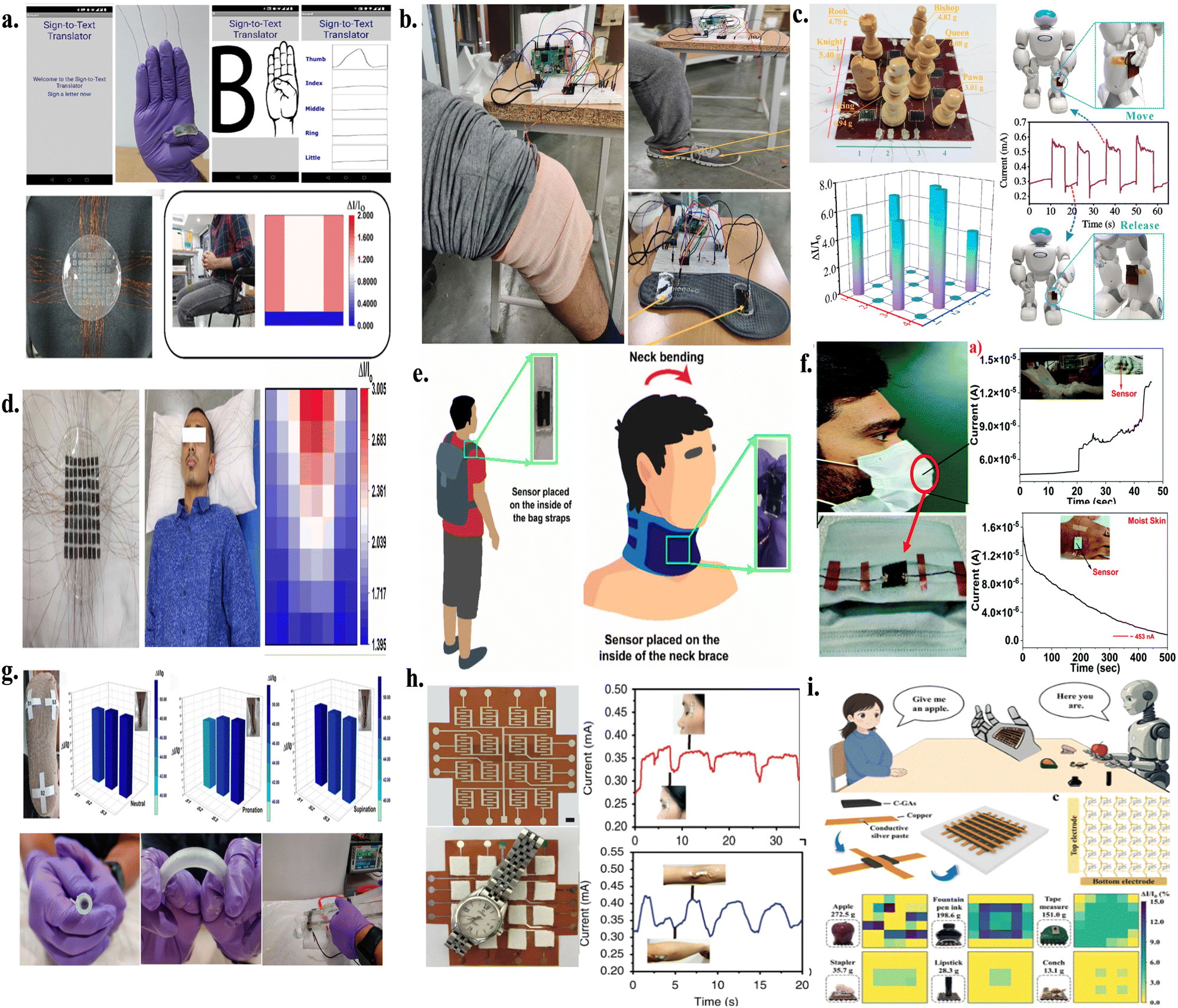 | ||
| Fig. 11 2D material-based human–machine interaction applications, (a) sign to text translation and posture analysis utilizing nanohybrid 2D materials, reproduced from ref. 105 Copyright 2022, the American Chemical Society. (b) Smart shoe and crepe bandage for human-motion monitoring, reproduced from ref. 113 Copyright 2022, the American Chemical Society. (c) Array sensor for the detection of position response to motion behaviour, reproduced from ref. 53 Copyright 2020, the American Chemical Society. (d) Tetraplegia call detection system as smart pillow, (e) load detection and cervical collar strain alert system flexible strain sensor, and (f) smart mask for breathing monitoring and baby diaper wetting detection system reproduced from ref. 174 Copyright New Journal of Chemistry. (g) Gait detection and monitoring fluid biomimetic tube, reproduced from ref. 173 Copyright 2021, the American Chemical Society. (h) Sensor array to detect pressure distribution and minimal strain change due to eye blinking and elbow bending, reproduced from ref. 170 Copyright Nature Communication. (i) Multiplex detection of magnitude, direction and contact location using sensor array, reproduced from ref. 169 Copyright the American Chemical Society. | ||
6.2 Artificial e-skin: mimicking human skin for advanced applications
Human skin, the body's largest organ, plays a vital role in detecting pressure, temperature, and various external stimuli. Its sensory functions are being emulated through electronic systems, advancing e-skin development for use in robotics, AI, and human–machine interface. To achieve this, the creation of artificial electronic skin (e-skin) has shown great promise. E-skin is intended to mimic the sensory functions of human skin, while also improving its capabilities with advanced electronics. This technology has numerous potential applications in areas such as human–machine interfaces, robotics, artificial intelligence, and prosthetics. Nevertheless, developing fully operational e-skin requires materials that demonstrate excellent mechanical flexibility, various electrical properties, and compatibility with flat fabrication methods. Recent advancements in 2D materials, such as graphene, TMDs, and MXenes, have significantly contributed to the development of high-performance e-skin systems.Noncontact e-skin, which mimics the long-range sensory characteristics of human skin, is becoming essential for fully replicating human sensation in prosthetics and robotics. For instance, An et al. demonstrated the use of femtosecond laser direct writing to produce highly flexible noncontact e-skins with sophisticated designs.178 This approach shows promise for wearable human–machine interfaces, bioelectronics, and robotics applications. Similarly, an all-graphene, flexible, in-plane e-skin was developed to mimic the noncontact sensing capabilities of human skin, while maintaining conformal contact with a human hand. These advancements pave the way for improvements in noncontact e-skin technologies, enabling high-spatial-resolution sensing and long-range detection. Ultrathin, flexible tactile sensors that can closely conform to surfaces are vital for the evolution of wearable devices, e-skin, and biorobotics. However, conventional passive sensors often experience signal interference or crosstalk, which compromises their sensing precision and restricts their applicability in complex tasks. Thus, to address this limitation, Park et al.179 (2019) introduced an active matrix tactile sensor featuring an 8 × 8 array structure built with two-dimensional MoS2.179 This device effectively recognized multiple simultaneous touch points, traced stylus movements, and identified object shapes during human grasping. In a related development, Kang et al.189 (2017) engineered a stretchable, skin-conformable touch sensor using graphene, designed for mutual capacitance sensing.180 This sensor could detect multiple touches both with and without physical contact and was functional when applied directly to flexible body areas such as the forearm and palm, emphasizing its potential for integration into wearable systems.
To replicate the physical, chemical, and sensory characteristics of human skin, next-generation advanced e-skin needs to possess features such as stretchability, self-healing capabilities, biocompatibility, biodegradability, and other enhanced functional properties. Wang et al. reported the progress in e-skin technologies in three main applications, including skin-attachable electronics, robotics and prosthetics. A soft, flexible sensor with integrated circuits, e-skin was reported by the Bao research group at Stanford University. This technology has the potential to create coverings for prosthetic limbs that can offer users a sense of touch or aid in regaining sensation for those with skin damage.181 Duan et al. (2023) developed a human-like hyper-attribute gel skin sensor that incorporates all the desirable skin-like properties, including stretchability, self-healing, biocompatibility, and antibacterial activities.182 This sensor also demonstrated sensory capabilities for pressure, temperature, humidity, strain, contact, and function reconfigurability and evolvability. These advancements bring e-skins closer to replicating the full range of human skin functionalities, making them suitable for robotics and skin-attachable wearables. However, enhancing the sensitivity and range of these sensors continues to be a major challenge. In 2021, Adepu et al. developed a highly sensitive, large-area sensor array using Ti3C2Tx deposited on polyurethane foam. This multifunctional sensor was designed to detect a range of physical stimuli, such as pressure, temperature, and strain. It was seamlessly integrated into wearable systems for applications including object localization, gesture recognition, and thermal monitoring, highlighting its promising potential for use in artificial skin technologies.183 Ti3C2Tx-based nanohybrids have emerged as highly promising materials for the fabrication of artificial e-skin, owing to their excellent sensitivity, mechanical flexibility, and durability. In 2023, Adepu et al. developed a flexible piezoresistive pressure sensor using an MoSe2/Ti3C2Tx nanohybrid, achieving high sensitivity and stable performance.106 Configured as a 7 × 7 matrix, the sensor was applied to a human hand to validate its functionality in tactile sensing, demonstrating its viability as artificial skin. For instance, a soft, flexible sensor with integrated circuits, e-skin, was reported by the Bao research group at Stanford University. This technology can pave the way for developing coverings for prosthetic limbs that would enable wearers to experience a sense of touch or assist in recovering sensation in individuals with compromised skin.
In conclusion, the rapid advancement of artificial e-skin has been strongly influenced by breakthroughs in 2D materials such as graphene, TMDs, and MXenes due to their superior electrical conductivity, mechanical flexibility, and tunable surface chemistry, which make them ideal for engineering multifunctional e-skin systems. These technologies, encompassing contactless sensing, flexible tactile interfaces, high sensitivity pressure sensors, and biomimetic gels, are driving innovation across robotics, prosthetics and wearable electronics (Table 4). As research continues, the integration of 2D materials into e-skin systems will enable more sophisticated and versatile applications, bringing us closer to fully replicating the sensory capabilities of human skin (Fig. 12).
| Sensor type | 2D materials & material composition | Applications | Sensitivity | Response time | Stability | Ref. |
|---|---|---|---|---|---|---|
| Piezoresistive sensor | MoSe2/Ti3C2Tx | E-skin applications | 14.70 kPa−1 | — | 2500 cycles | 106 |
| Ferroelectric sensor | rGO/PVDF | Multilayer e-skin | 47.7 kPa−1 | 20 ms | 5000 cycles | 184 |
| Strain sensor | Graphene | E-skin tactile sensing | GF ∼ 500 | 10–30 ms | — | 185 |
| MXene sensor | MXene | In vivo biomonitoring | 164.75 kPa−1 | — | — | 186 |
| Hygel e-skin | MXene | Gesture recognition and interactive control | GF ∼ 9.2 | — | — | 182 |
| Pressure sensor | MXene | Monitoring human activities and soft robots gripper | High | 98 s | 10000 cycles |
187 |
| Humidity sensor | WS2 | E-skin based humidity sensor | Up to 2357 | — | — | 188 |
| Strain sensor | Ti3C2Tx | Detect temperature, identify object and position, capture gesture | ∼34.24 kPa−1 | — | 2500 cycles | 183 |
| Tactile sensor | MoS2 | Skin attachable active textile sensor | 0.011 kPa−1 | 180 ms | 155 | |
| Capacitive | Graphene | Auxetic touch sensor | 200 cycles | 189 | ||
| Tactile sensors | MoS2 | E-skin application | 10000 cycles |
179 | ||
| Pressure sensor | MXene | E-skin application | 99.5 kPa−1 | 11 ms | 10000 cycles |
190 |
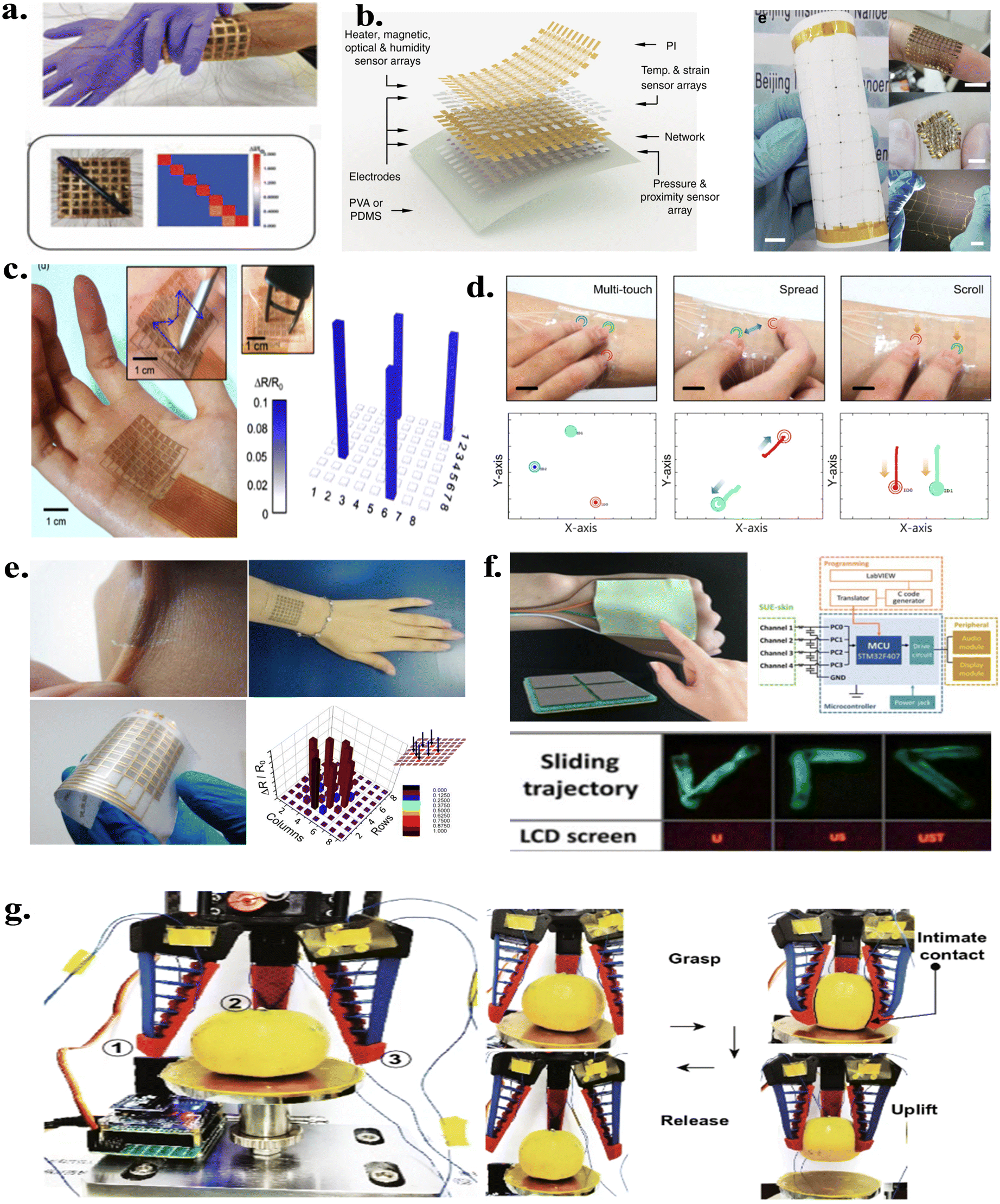 | ||
| Fig. 12 2D material-based e-skin applications. (a) MXene/MoSe2 nanohybrid-based flexible pressure sensor array, reproduced from ref. 106 Copyright Applied Physics Letters. (b) Skin-inspired highly stretchable and conformable matrix networks, reproduced from ref. 191 Copyright from Nature Communication. (c) MoS2-based skin attachable active matrix textile sensor array, reproduced from ref. 155 Copyright the American Chemical Society. (d) Graphene-based stretchable auxetic touch sensor, reproduced from ref. 189 Copyright the American Chemical Society. (e) Graphene woven microfabric sensor arrays for a strain sensor, reproduced from ref. 185 Copyright the American Chemical Society. (f) E-skin demonstration of touch operation and displaying the characters, reproduced from ref. 192 Copyright from Science Advances. (g) Hyper attributed gel for multifunctional sensing on robot, reproduced from ref. 193 Copyright from Nano-Micro Letters. (h) Soft bio integrated e-skin system, reproduced from ref. 181 Copyright from Science.org. | ||
6.3 Machine learning and artificial intelligence in sensor applications
Additionally, Adepu et al. reported the fabrication of a sensors that can convert signs into text translation and analyze sitting positions using electromechanical sensors based on an SnS/Ti3C2Tx nanohybrid.105 These sensors exhibit the properties to evaluate the customer or user sitting posture and offer feedback using machine learning algorithms, which can help mitigate health issues such as back pain and spinal deformities. By training artificial intelligence models to identify specific movements or postures, it is possible to convert sign language into text in real-time and alert users when they are sitting incorrectly. This technology has the potential to greatly improve workplace ergonomics and enhance the quality of life for individuals with disabilities. AI and 2D materials together also make it possible to create intelligent systems that can monitor health in real time. Real-time anomaly detection is possible with MXene-based sensors that are coupled with AI algorithms to monitor human physiological signals including heart rate, respiration rate, and muscle activity.194 In healthcare applications, where early health issue diagnosis can greatly enhance patient outcomes, this skill is especially helpful. For instance, AI-enhanced sensors can be used to track patients with long-term illnesses, giving medical professionals constant feedback and facilitating prompt actions. These systems are very effective for long-term usage because they can process data immediately on the sensor, which lowers the latency and energy consumption.195,196 More complex object handling and environmental interaction in robotics have been made possible by the combination of flexible sensors with machine learning and artificial intelligence. Robots with AI-enhanced sensors are more efficient and adaptable in dynamic environments because they can identify and handle things of different weights and forms.51 For example, robots in industrial environments can employ these sensors to identify product flaws or carry out precise assembly tasks. Also, AI in autonomous cars can enhance the performance and safety of sensors by improving navigation and obstacle recognition (Fig. 13). | ||
| Fig. 13 2D material-based flexible and wearable sensors in consumer electronics application, (a) MXene/NiSe2-based pressure sensor as a smart bed for real-time monitoring of sleep tracking, reproduced from ref. 176 Copyright from Advanced Materials Interfaces. (b) TeNW/MXene nanohybrid-based flexible sensor for wireless monitoring and communication, reproduced from ref. 104 Copyright from the American Chemical Society. (c) MXene-based flexible and conformal antenna for pressure and level sensing,197 Copyright Elsevier FlatChem. (d) Pressure sensor-based smart tactile gloves and pedometer, reproduced from ref. 198 Copyright from Elsevier Sensor and Actuators. | ||
The application of AI and machine learning is transforming environmental sensing technologies. With the integration of flexible sensors and AI algorithms, it is now possible to monitor environmental factors such as temperature, humidity, and air quality in real-time. These sensors can be deployed in smart cities to enhance pollution management and resource usage through continuous monitoring and data analysis. For example, AI-powered sensors are capable of detecting changes in air quality and can trigger automated responses or alerts, such as redirecting traffic to reduce emissions or adjusting ventilation systems in buildings. Moreover, the rise of flexible electronics catering to internet of things (IoT) applications has led to a growing demand for flexible antennas in wearable devices and communication systems. Unlike traditional rigid antennas, flexible antennas can conform to curved surfaces, withstand mechanical stress, and seamlessly integrate with wearable technology. In particular, MXene-based flexible antennas have gained attention due to their outstanding conductivity, mechanical flexibility, and dual functionality as both sensors and communication devices. For example, Sindhu et al. (2022) introduced an affordable MXene-based patch antenna capable of sensing pressure and levels, opening new possibilities in fields such as industrial monitoring, security, and healthcare.197 To enable real-time data transmission and sensing capabilities, these antennas can be incorporated into industrial IoT systems, smartwatches, or smart clothing. Flexible antennas are revolutionizing wearable diagnostics and remote patient monitoring in healthcare. When integrated into devices such as fitness trackers and smart bandages, they can send data to healthcare professionals while tracking vital signs such as heart rate, respiration rate, and activity levels. These antennas also support asset tracking and predictive maintenance in industrial settings through real-time monitoring of equipment conditions. Additionally, their integration with AI and machine learning enhances functionality, allowing anomaly detection, personalized feedback, and predictive analytics. For instance, AI systems can utilize physiological signals from flexible antennas to assess data, predict equipment failures, or provide health recommendations. However, although flexible sensors show great promise, challenges remain in effectively integrating with them machine learning (ML) and artificial intelligence (AI), along with ensuring robustness, signal integrity, and low power consumption in flexible antennas. The key challenges include the energy required for AI algorithms, the computational demands of real-time data processing, and the necessity for large datasets for training AI models. Thus, future research should focus on optimizing designs, exploring innovative materials with enhanced sensing abilities, and incorporating advanced features such as energy harvesting, self-healing, and edge computing for efficient data processing at the sensor level. As the industry evolves, the combination of flexible antennas and AI-enhanced sensors is poised to significantly benefit areas such as wearable electronics, intelligent systems, and the internet of things. These technological advancements will drive progress in environmental monitoring, healthcare, and security, ultimately improving the operational efficiency and quality of life. In conclusion, flexible pressure sensors combined with artificial intelligence and machine learning have created new opportunities for their cutting-edge use in robotics, wearable electronics, healthcare, and environmental sensing.
By leveraging AI algorithms, these sensors can perform complex tasks such as object recognition, health monitoring, and real-time decision-making, significantly enhancing their functionality and application scope. As research in this field continues to evolve, AI-enhanced flexible sensors are poised to play a pivotal role in the development of next-generation smart systems.
6.4 In-sensor computing: revolutionizing sensing and processing
In-sensor computing, often referred to as near-sensor computing, signifies a revolutionary advancement in how sensing and processing are incorporated into electronic systems. In contrast to traditional configurations, where sensors collect data and send it to a separate processing unit, in-sensor computing combines both sensing and computing capabilities into a single device. This integrated approach reduces the need for frequent data transfer between sensors and processors, resulting in lower system complexity, decreased energy consumption, and reduced latency. The rapid proliferation of sensor nodes in the internet of things generates a substantial volume of data at the sensory terminals. Frequent data transfer between sensors and computing units severely limit the system performance in terms of speed, security, and energy efficiency. Therefore, it is crucial to develop a new computational paradigm that integrates computational capabilities into sensor networks to efficiently process large amounts of sensory input. By processing data locally, the in-sensor computing paradigm minimizes both the computational complexity and data transit.Significant attention has been focused on using 2D semiconductor materials to create more compact and efficient sensor circuits. These materials, which use their intrinsic ambipolar transport capabilities, include electrostatically doped silicon, two-dimensional WSe2, PtSe2, and MoTe2/PdSe2 heterostructures. Furthermore, using ferroelectric materials, which are well-known for their low power consumption and non-volatility, is essential for the advancement of in-sensor computing technologies. To create novel retinomorphic sensors, the ferroelectric and photoconductive properties of two-dimensional materials such as SnS2 and α-In2Se3 have been explored in the literature. By using switchable polarisation dipoles, these ferro-photonic AI chips allow electrical programming and optical stimulation of the channel to change the polarisation state, allowing multifunctional functioning.
Multimodal processing in in-sensor computing refers to the integration and simultaneous handling of various types of sensory data within a single sensor system. This approach enables the sensor to record and interpret different types of data, including tactile, visual, and audio information. For instance, a multimodal in-sensor computing system might combine sound data from a microphone, depth information from an LiDAR sensor, and image data from a camera sensor. By incorporating these diverse types of data, the system can detect a wider range of sensory inputs, provide thorough real-time analyses, reduce the need for data transfer to external processors, and enhance the overall system efficiency. Additionally, the integration of touch and taste information contributes to a more accurate understanding of the environment. Applications of this technology include autonomous vehicles, where combining visual and depth data can significantly improve object detection and navigation, as well as smart devices that aim to interact with users in a more responsive and intuitive manner. For example, in self-driving cars, where every millisecond is crucial for safety, in-sensor computing plays a vital role by handling data instantly. The sensors in these vehicles must swiftly identify pedestrians, obstacles, and other cars, enabling them to make immediate decisions without the need for additional processing units. By allowing for the analysis of visual and environmental data at the sensor level, in-sensor computing reduces the latency and improves the overall system performance.199,200
Besides, biomimetic research has created in-sensor computing devices that replicate natural processes, drawing inspiration from biological systems. For example, Liao et al. (2022) created a lobule giant movement detector (LGMD) influenced by insect collision-avoidance techniques. Traditionally implemented using very-large-scale-integration (VLSI) systems, the LGMD was recently emulated using a single device comprised of a monolayer MoS2 photodetector stacked on top of a floating-gate memory device. This device mimics the behavior of LGMD neurons, showcasing the potential of 2D materials for biomimetic in-sensor computing.199,201 Also Yang et al.164 (2024) employed a graphene/Ge heterostructure to construct an in-sensor dynamic computing system capable of robustly tracking dim targets. The system utilizes a dynamic kernel through an optoelectronic device array, dynamically adjusting the photoresponse via variable gate voltages. This array responds to spatial light patterns and contains internal correlations, enabling advanced computational tasks directly at the sensor level. Applications where real-time processing of visual input is essential, such as autonomous navigation, surveillance, and environmental monitoring, benefit greatly from these systems.201 Additionally, Liao et al. (2022) used MoS2 phototransistors to establish an in-sensor visual adaptation system that replicates the dynamic regulation of photosensitivity in the human retina under various light conditions. This technique greatly increases the accuracy of image recognition, while also improving the image contrast by deliberately creating defect states in MoS2 phototransistors through ultraviolet-ozone (UVO) treatment, where ambipolar trap states form in the bandgap, resulting in adaptive visual behavior. This technique showcases the potential of 2D materials for developing adaptive sensing systems that function efficiently in different lighting environments.202 Advancements in 2D material-based sensor computing technologies have led to the creation of compact, energy-efficient hardware capable of local data processing and neuromorphic computation. These technologies are integral for developing intelligent systems for robotics, healthcare, and the internet of things. 2D materials, such as MoS2, WSe2, and PtSe2, offer exceptional electronic, optical, and mechanical properties, enabling the fabrication of advanced devices such as phototransistors and gas sensors with built-in computational capabilities.28,165,203 Recent research utilizes unique phenomena in these materials to create multifunctional devices that perform various tasks, including motion detection and brain-inspired computing.
In summary, a significant development in sensing and processing, in-sensor computing, provides a more integrated and effective method than conventional systems. 2D materials such as graphene, MoS2, and MXene have special qualities that make them perfect for in-sensor computing systems. These materials facilitate the creation of novel devices that can carry out intricate calculations directly at the sensor level, ranging from biomimetic collision detection and dynamic target tracking to visual adaptation and artificial synapse arrays. In-sensor computing systems have the potential to transform robotics, healthcare, environmental monitoring, and other applications as research in this area advances, opening the door for more intelligent and effective technology.
7. Challenges in the sensor community
Despite the significant advancements, wearable and flexible sensors based on 2D materials still face critical challenges. Mechanical deformation such as bending, stretching, and twisting can degrade the sensitivity, stability, and signal fidelity of sensors. Thus, ensuring a reliable performance under dynamic conditions, especially in biomedical and robotic applications, remains difficult. Additionally, environmental factors such as humidity and temperature fluctuations can interfere with signal outputs, necessitating robust encapsulation and compensation strategies. Multimodal sensing systems also suffer from signal cross-talk, making it challenging to accurately decouple and interpret pressure, strain, and temperature signals. Addressing these issues requires innovative material integration, precise structural design, and improved signal processing techniques to fully leverage the potential of 2D materials in next-generation flexible sensors. Also, advanced signal processing algorithms and machine learning techniques are required to decouple and accurately interpret multiple stimuli. Lastly, the cost-effectiveness of 2D materials and their fabrication processes must be addressed to make these technologies accessible for mass-market adoption. Overcoming these challenges will require interdisciplinary collaboration, innovative material engineering, and advancements in fabrication technologies to unlock the full potential of 2D materials in next-generation wearable and flexible sensors.8. Author perspective for the next 10 years in 2D material-based sensor research
Several next-generation 2D materials have been theoretically predicted and are attracting significant interest for their potential in advanced electronics, optoelectronics, and quantum technologies, although many have not yet been fully synthesized or characterized experimentally. Notable examples include group VA elemental monolayers such as antimonene, arsenene, and bismuthene, which are predicted to exhibit unique electronic and topological properties. Beyond these, the large family of transition metal carbides and nitrides known as MXenes has been computationally designed, with around 70 new MXene compositions predicted to possess tunable electronic, magnetic, and catalytic features. The discovery of double transition metal MXenes (DTM MXenes), another subclass of the MXene family, was reported in 2015. Babak et al. validated this subclass through DFT studies, and later proved their existence by synthesising Mo2TiC2Tx, Mo2Ti2C3Tx and Cr2TiCxTx and demonstrating the electromechanical behaviour of Mo2TiC2Tx. These findings significantly broadened the compositional and functional landscape of MXene materials, which have potential applications in energy, catalysis and beyond and have not been studied for sensing applications.204 Other theoretically promising materials include borophene (2D boron), 2D topological insulators, and various layered dichalcogenides and dichlorides, each offering exceptional conductivity, flexibility, and in some cases, intrinsic magnetism or superconductivity. MBenes are another new 2D family (transition metal borides), which have a structure analogous to that of MXenes. Recently, theoretical and experimental studies have highlighted their potential for various applications, including electrocatalysts, HER, nitrogen reduction, batteries and supercapacitors, due to the presence of surface functionalization and favourable ion transport capabilities. However, challenges remain in their scalable synthesis, structural control, long-term stability and much of their potential both theoretically and experimentally.205,206 Machine learning and advanced quantum simulations are accelerating the discovery of these materials, but their experimental realisation is often limited by their complex atomic arrangements, challenging synthesis conditions, and stability issues under ambient conditions. As computational methods and synthesis techniques advance, these next-generation 2D materials are poised to play a transformative role in future device technologies.Currently, although 2D material-based sensing technology is in its infancy, these materials have significantly progressed. There are commercial products for mass graphene production and also TMDs. This will definitely lower their cost, and the next obvious thing will be to take 2D material-based sensors to the market. We envision that this will happen in the coming decade. Also, despite their commercialization, the research on 2D material-based sensors will continue and reach exciting paths. The future of 2D material-based flexible sensors lies in the convergence of quantum-enhanced sensing, AI-driven adaptability, and self-powered operation, paving the way for highly autonomous and intelligent systems. By integrating van der Waals heterostructures with bound states in the continuum (BIC) structures, next-generation sensors will achieve unprecedented sensitivity for wearable quantum biosensors and high-resolution medical imaging. AI-powered platforms will enable self-learning, real-time calibration, and predictive analytics, transforming applications such as electronic skin, smart textiles, and neuromorphic interfaces for robotics and human–computer interactions. Additionally, piezoelectric and triboelectric nanogenerators based on materials such as MoS2 and graphene will enable the fabrication of energy-autonomous sensors, eliminating the need for batteries in wearables, IoT devices, and space exploration technologies. As research advances, atomic-level engineering of MXenes, Janus 2D materials, and hybrid heterostructures will further enhance the performance of devices, leading to ultra-sensitive molecular biosensors and hyper-flexible bioelectronics. With these breakthroughs, 2D material-based flexible sensors will revolutionize healthcare, environmental monitoring, and next-generation soft robotics, enabling a future where sensing systems seamlessly integrate with both the human body and the surrounding environment. However, although some technologies will hit market in the coming decade, there is a long way ahead for research on 2D material-based sensors combining quantum and artificial intelligence. Fig. 14 shows the lab 2D material-based sensor prototype developed in our lab.
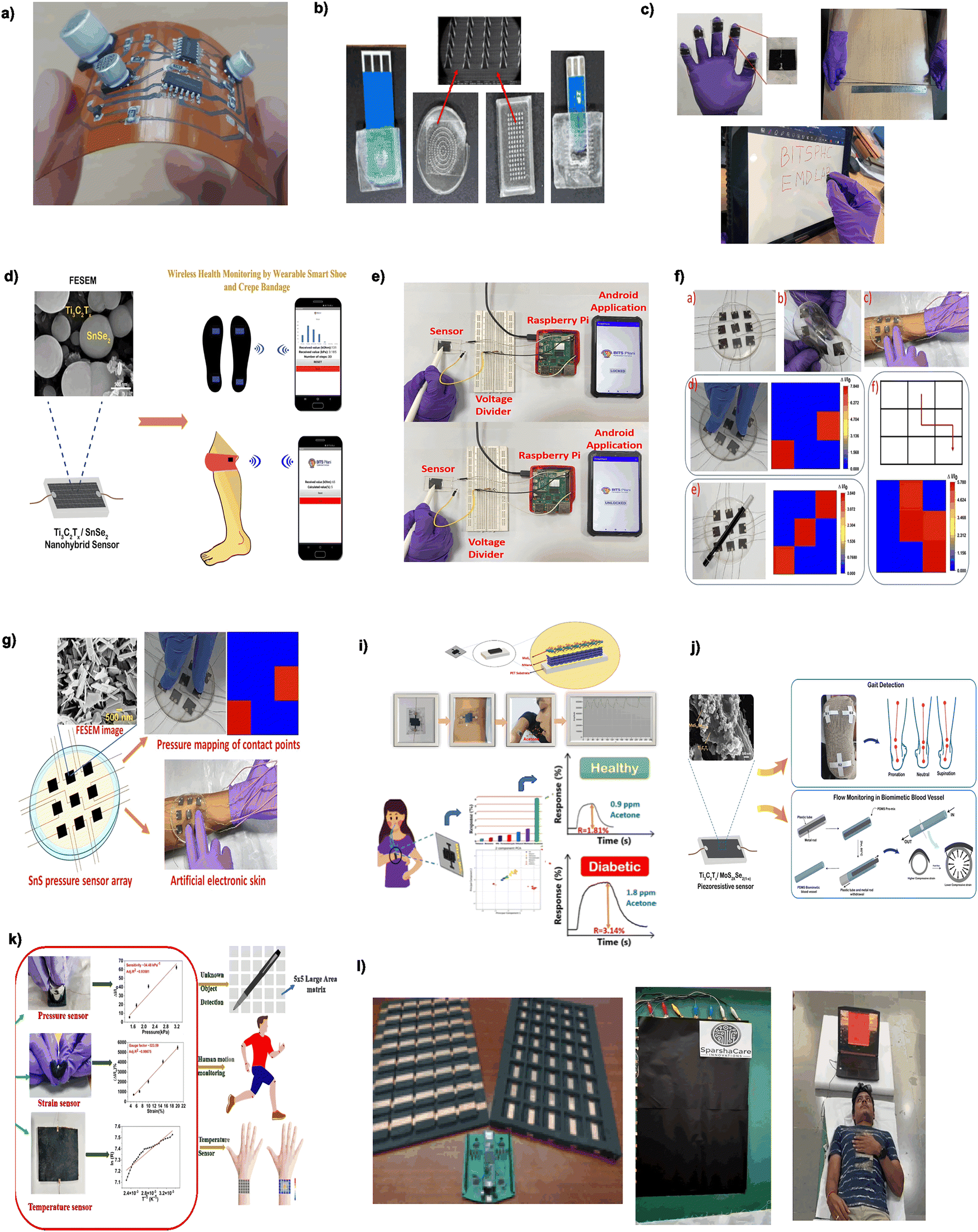 | ||
| Fig. 14 Laboratory prototype of the (a–l) different 2D material-based sensor developed in our lab. | ||
Conflicts of interest
There are no conflicts to declare.Data availability
The data supporting this article have been included within the manuscript.References
- Y. Lei, T. Zhang, Y. C. Lin, T. Granzier-Nakajima, G. Bepete, D. A. Kowalczyk, Z. Lin, D. Zhou, T. F. Schranghamer, A. Dodda, A. Sebastian, Y. Chen, Y. Liu, G. Pourtois, T. J. Kempa, B. Schuler, M. T. Edmonds, S. Y. Quek, U. Wurstbauer, S. M. Wu, N. R. Glavin, S. Das, S. P. Dash, J. M. Redwing, J. A. Robinson and M. Terrones, ACS Nanosci. Au, 2022, 2, 450–485 CrossRef CAS.
- Y. Zhou, M. Zhang, Z. Guo, L. Miao, S. T. Han, Z. Wang, X. Zhang, H. Zhang and Z. Peng, Mater. Horiz., 2017, 4, 997–1019 RSC.
- D. Jiang, Z. Liu, Z. Xiao, Z. Qian, Y. Sun, Z. Zeng and R. Wang, J. Mater. Chem. A, 2022, 10, 89–121 RSC.
- T. Du, X. Han, X. Yan, J. Shang, Y. Li and J. Song, Adv. Mater. Technol., 2023, 8, 2202029, DOI:10.1002/admt.202202029.
- W. Zhai, Z. Li, Y. Wang, L. Zhai, Y. Yao, S. Li, L. Wang, H. Yang, B. Chi, J. Liang, Z. Shi, Y. Ge, Z. Lai, Q. Yun, A. Zhang, Z. Wu, Q. He, B. Chen, Z. Huang and H. Zhang, Chem. Rev., 2024, 124, 4479–4539 Search PubMed.
- K. Belay Ibrahim, T. Ahmed Shifa, S. Zorzi, M. Getaye Sendeku, E. Moretti and A. Vomiero, Prog. Mater. Sci., 2024, 144, 101287 CrossRef CAS.
- W. Huang, L. Hu, Y. Tang, Z. Xie and H. Zhang, Adv. Funct. Mater., 2020, 30, 2005223, DOI:10.1002/adfm.202005223.
- M. Naguib, V. N. Mochalin, M. W. Barsoum and Y. Gogotsi, Adv. Mater., 2014, 26, 992–1005 CrossRef CAS.
- B. Anasori, C. Shi, E. J. Moon, Y. Xie, C. A. Voigt, P. R. C. Kent, S. J. May, S. J. L. Billinge, M. W. Barsoum and Y. Gogotsi, Nanoscale Horiz., 2016, 1, 227–234 RSC.
- A. Ahmed, S. Sharma, B. Adak, M. M. Hossain, A. M. LaChance, S. Mukhopadhyay and L. Sun, InfoMat, 2022, 4(4) DOI:10.1002/inf2.12295.
- Y. Shao, L. Wei, X. Wu, C. Jiang, Y. Yao, B. Peng, H. Chen, J. Huangfu, Y. Ying, C. J. Zhang and J. Ping, Nat. Commun., 2022, 13, 1–8 Search PubMed.
- S. Fruncillo, X. Su, H. Liu and L. S. Wong, ACS Sens., 2021, 6, 2002–2024, DOI:10.1021/acssensors.0c02704.
- Y. Lee, S. Bae, H. Jang, S. Jang, S. E. Zhu, S. H. Sim, Y. Il Song, B. H. Hong and J. H. Ahn, Nano Lett., 2010, 10, 490–493 CrossRef CAS.
- Y. Ji, S. Lee, B. Cho, S. Song and T. Lee, ACS Nano, 2011, 5, 5995–6000 CrossRef CAS.
- X. Li, R. Zhang, W. Yu, K. Wang, J. Wei, D. Wu, A. Cao, Z. Li, Y. Cheng, Q. Zheng, R. S. Ruoff and H. Zhu, Sci. Rep., 2012, 2, 2025 Search PubMed.
- M. Kaltenbrunner, T. Sekitani, J. Reeder, T. Yokota, K. Kuribara, T. Tokuhara, M. Drack, R. Schwödiauer, I. Graz, S. Bauer-Gogonea, S. Bauer and T. Someya, Nature, 2013, 499, 458–463 Search PubMed.
- J. J. Park, W. J. Hyun, S. C. Mun, Y. T. Park and O. O. Park, ACS Appl. Mater. Interfaces, 2015, 7, 6317–6324 CrossRef CAS.
- D. H. Ho, Q. Sun, S. Y. Kim, J. T. Han, D. H. Kim and J. H. Cho, Adv. Mater., 2016, 28, 2601–2608 Search PubMed.
- S. Kabiri Ameri, R. Ho, H. Jang, L. Tao, Y. Wang, L. Wang, D. M. Schnyer, D. Akinwande and N. Lu, ACS Nano, 2017, 11, 7634–7641 CrossRef CAS.
- E. Torres Alonso, D. P. Rodrigues, M. Khetani, D. W. Shin, A. De Sanctis, H. Joulie, I. de Schrijver, A. Baldycheva, H. Alves, A. I. S. Neves, S. Russo and M. F. Craciun, npj Flexible Electron., 2018, 2, 41528 Search PubMed.
- Y. Wei, Y. Qiao, G. Jiang, Y. Wang, F. Wang, M. Li, Y. Zhao, Y. Tian, G. Gou, S. Tan, H. Tian, Y. Yang and T. L. Ren, ACS Nano, 2019, 13, 8639–8647 CrossRef CAS.
- L. Zhu, Y. Wang, D. Mei, W. Ding, C. Jiang and Y. Lu, ACS Appl. Mater. Interfaces, 2020, 12, 31725–31737 Search PubMed.
- H. J. Lee, J. C. Yang, J. Choi, J. Kim, G. S. Lee, S. P. Sasikala, G. H. Lee, S. H. K. Park, H. M. Lee, J. Y. Sim, S. Park and S. O. Kim, ACS Nano, 2021, 15, 10347–10356 Search PubMed.
- S. Zhang, A. Chhetry, M. A. Zahed, S. Sharma, C. Park, S. Yoon and J. Y. Park, npj Flexible Electron., 2022, 6, 41528 Search PubMed.
- L. Chen, F. Chen, G. Liu, H. Lin, Y. Bao, D. Han, W. Wang, Y. Ma, B. Zhang and L. Niu, Anal. Chem., 2022, 94, 7319–7328 Search PubMed.
- S. Ghosh, A. Pannone, D. Sen, A. Wali, H. Ravichandran and S. Das, Nat. Commun., 2023, 14, 41467 Search PubMed.
- M. A. Zahed, D. K. Kim, S. H. Jeong, M. Selim Reza, M. Sharifuzzaman, G. B. Pradhan, H. Song, M. Asaduzzaman and J. Y. Park, ACS Sens., 2023, 8, 2960–2974 Search PubMed.
- J. Huang, J. Feng, Z. Chen, Z. Dai, S. Yang, Z. Chen, H. Zhang, Z. Zhou, Z. Zeng, X. Li and X. Gui, Nano Energy, 2024, 126, 2025 Search PubMed.
- H. Jiang, L. Zheng, Z. Liu and X. Wang, InfoMat, 2020, 2, 1077–1094 CrossRef CAS.
- M. S. Mannoor, H. Tao, J. D. Clayton, A. Sengupta, D. L. Kaplan, R. R. Naik, N. Verma, F. G. Omenetto and M. C. McAlpine, Nat. Commun., 2012, 3, 763, DOI:10.1038/ncomms1767.
- S. E. Root, S. Savagatrup, A. D. Printz, D. Rodriquez and D. J. Lipomi, Chem. Rev., 2017, 117, 6467–6499 CrossRef CAS.
- H. Zhan, X. Tan, G. Xie and D. Guo, Small, 2021, 17, 1–9 Search PubMed.
- J. Zhao, Z. Chi, Z. Yang, X. Chen, M. S. Arnold, Y. Zhang, J. Xu, Z. Chi and M. P. Aldred, Nanoscale, 2018, 10, 5764–5792 Search PubMed.
- V. Yadav, S. Roy, P. Singh, Z. Khan and A. Jaiswal, Small, 2018, 15, 1803706, DOI:10.1002/smll.201803706.
- Y. Yang, X. Li, M. Wen, E. Hacopian, W. Chen, Y. Gong, J. Zhang, B. Li, W. Zhou, P. M. Ajayan, Q. Chen, T. Zhu and J. Lou, Adv. Mater., 2017, 29, 1–7 Search PubMed.
- S. Deng, L. Li and M. Li, Phys. E, 2018, 101, 44–49 CrossRef CAS.
- K. Liu, Q. Yan, M. Chen, W. Fan, Y. Sun, J. Suh, D. Fu, S. Lee, J. Zhou, S. Tongay, J. Ji, J. B. Neaton and J. Wu, Nano Lett., 2014, 14, 5097–5103 Search PubMed.
- L. Li, Y. Yu, G. J. Ye, Q. Ge, X. Ou and H. Wu, Nat. Nanotechnol., 2014, 9, 372–377 CrossRef CAS.
- H. Wang, Q. Li, Y. Gao, F. Miao, X. F. Zhou and X. G. Wan, New J. Phys., 2016, 18, 073016, DOI:10.1088/1367-2630/18/7/073016.
- C. Rong, T. Su, Z. Li, T. Chu, M. Zhu, Y. Yan, B. Zhang and F. Z. Xuan, Nat. Commun., 2024, 15, 1566, DOI:10.1038/s41467-024-45657-6.
- F. Schwierz, J. Pezoldt and R. Granzner, Nanoscale, 2015, 7, 8261–8283 RSC.
- N. D. Robert Cronin Yung Peng, Rose Khavari and G. O. D. P. J. S. J. M. C. F. R. N. Kate Shannon., Physiol. Behav., 2016, 176, 139–148 Search PubMed.
- X. Zhang, X. Zhao, D. Wu, Y. Jing and Z. Zhou, Nanoscale, 2015, 7, 16020–16025 RSC.
- H. Lashgari, A. Boochani, A. Shekaari, S. Solaymani, E. Sartipi and R. T. Mendi, Appl. Surf. Sci., 2016, 369, 76–81 Search PubMed.
- A. Kuc, N. Zibouche and T. Heine, Phys. Rev. B:Condens. Matter Mater. Phys., 2011, 83, 1–4 CrossRef.
- J. K. Ellis, M. J. Lucero and G. E. Scuseria, Appl. Phys. Lett., 2011, 99, 261908, DOI:10.1063/1.3672219.
- A. Chaves, J. G. Azadani, H. Alsalman, D. R. da Costa, R. Frisenda, A. J. Chaves, S. H. Song, Y. D. Kim, D. He, J. Zhou, A. Castellanos-Gomez, F. M. Peeters, Z. Liu, C. L. Hinkle, S. H. Oh, P. D. Ye, S. J. Koester, Y. H. Lee, P. Avouris, X. Wang and T. Low, npj 2D Mater. Appl., 2020, 29 DOI:10.1038/s41699-020-00162-4.
- N. Higashitarumizu, S. Z. Uddin, D. Weinberg, N. S. Azar, I. K. M. Reaz Rahman, V. Wang, K. B. Crozier, E. Rabani and A. Javey, Nat. Nanotechnol., 2023, 18, 507–513 CrossRef CAS.
- J. Miao and T. Fan, Carbon, 2023, 202, 495–527 CrossRef CAS.
- V. Selamneni, S. Sukruth and P. Sahatiya, FlatChem, 2022, 33, 100379 CrossRef CAS.
- H. Niu, F. Yin, E. S. Kim, W. Wang, D. Y. Yoon, C. Wang, J. Liang, Y. Li and N. Y. Kim, InfoMat, 2023, 5, 1–56 CrossRef.
- S. K. Chakraborty, B. Kundu, B. Nayak, S. P. Dash and P. K. Sahoo, iScience, 2022, 25, 103942 CrossRef CAS.
- Y. Cheng, Y. Ma, L. Li, M. Zhu, Y. Yue, W. Liu, L. Wang, S. Jia, C. Li, T. Qi, J. Wang and Y. Gao, ACS Nano, 2020, 14, 2145–2155 CrossRef CAS.
- S. Zhang, A. Chhetry, M. A. Zahed, S. Sharma, C. Park, S. Yoon and J. Y. Park, npj Flexible Electron., 2022, 6, 1–12 CrossRef.
- P. Z. Jiang, Z. Deng, P. Min, L. Ye, C. Z. Qi, H. Y. Zhao, J. Liu, H. Bin Zhang and Z. Z. Yu, Nano Res., 2024, 17, 1585–1594 CrossRef CAS.
- A. G. Kelly, D. Finn, A. Harvey, T. Hallam and J. N. Coleman, Appl. Phys. Lett., 2016, 109, 1–7 CrossRef.
- V. Shanmugam, R. A. Mensah, K. Babu, S. Gawusu, A. Chanda, Y. Tu, R. E. Neisiany, M. Försth, G. Sas and O. Das, Part. Part. Syst. Charact., 2022, 39, 2200031, DOI:10.1002/ppsc.202200031.
- X. Chen, X. Lu, B. Deng, O. Sinai, Y. Shao, C. Li, S. Yuan, V. Tran, K. Watanabe, T. Taniguchi, D. Naveh, L. Yang and F. Xia, Nat. Commun., 2017, 8, 1–7 CrossRef.
- J. Chen, G. Ma, X. Wang, T. Song, Y. Zhu, S. Jia, X. Zhang, Y. Zhao, J. Chen, B. Yang and Y. Li, Nanoscale, 2024, 16, 5999–6009 RSC.
- H. Kim, S. Z. Uddin, D. H. Lien, M. Yeh, N. S. Azar, S. Balendhran, T. Kim, N. Gupta, Y. Rho, C. P. Grigoropoulos, K. B. Crozier and A. Javey, Nature, 2021, 596, 232–237 CrossRef CAS.
- X. Cai, Y. Luo, B. Liu and H. M. Cheng, Chem. Soc. Rev., 2018, 47, 6224–6266 RSC.
- K. F. Mak, C. Lee, J. Hone, J. Shan and T. F. Heinz, Phys. Rev. Lett., 2010, 105, 2–5 CrossRef.
- Y. Tian, A. Sun, Z. Ge, Y. Zhang, S. Huang, S. Lv and H. Li, Chem. Phys. Lett., 2021, 765, 138286 CrossRef CAS.
- A. Thin, ACS Nano, 2013, 791–797 Search PubMed.
- C. Cong, J. Shang, Y. Wang and T. Yu, Adv. Opt. Mater., 2018, 6, 1–15 Search PubMed.
- H. Zhou, C. Wang, J. C. Shaw, R. Cheng, Y. Chen, X. Huang, Y. Liu, N. O. Weiss, Z. Lin, Y. Huang and X. Duan, Nano Lett., 2015, 15, 709–713 CrossRef CAS.
- Y. Wang, L. Li, W. Yao, S. Song, J. T. Sun, J. Pan, X. Ren, C. Li, E. Okunishi, Y. Q. Wang, E. Wang, Y. Shao, Y. Y. Zhang, H. T. Yang, E. F. Schwier, H. Iwasawa, K. Shimada, M. Taniguchi, Z. Cheng, S. Zhou, S. Du, S. J. Pennycook, S. T. Pantelides and H. J. Gao, Nano Lett., 2015, 15, 4013–4018 Search PubMed.
- S. Aftab, A. A. Al-Kahtani, M. Z. Iqbal, S. Hussain and G. Koyyada, Adv. Mater. Technol., 2023, 8, 1–21 Search PubMed.
- X. Cao, H. Chen, X. Gu, B. Liu, W. Wang, Y. Cao, F. Wu and C. Zhou, ACS Nano, 2014, 8, 12769–12776 CrossRef CAS.
- A. Mishra, P. K. Singh, N. Chauhan, S. Roy, A. Tiwari, S. Gupta, A. Tiwari, S. Patra, T. R. Das, P. Mishra, A. S. Nejad, Y. K. Shukla, U. Jain and A. Tiwari, Sens. Diagn., 2024, 3, 718–744 RSC.
- C. W. Lin, Z. Zhao, J. Kim and J. Huang, Sci. Rep., 2014, 4, 1–6 Search PubMed.
- R. Chen, X. Wang, X. Li, H. Wang, M. He, L. Yang, Q. Guo, S. Zhang, Y. Zhao, Y. Li, Y. Liu and D. Wei, Sci. Adv., 2021, 7, 1–9 Search PubMed.
- H. Minemawari, T. Yamada, H. Matsui, J. Y. Tsutsumi, S. Haas, R. Chiba, R. Kumai and T. Hasegawa, Nature, 2011, 475, 364–367 CrossRef CAS.
- B. Mendoza-Sánchez, J. Coelho, A. Pokle and V. Nicolosi, Electrochim. Acta, 2016, 192, 1–7 CrossRef.
- S. Naficy, R. Jalili, S. H. Aboutalebi, R. A. Gorkin, K. Konstantinov, P. C. Innis, G. M. Spinks, P. Poulin and G. G. Wallace, Mater. Horiz., 2014, 1, 326–331 RSC.
- K. Jasmine, Penambahan Natrium Benzoat Dan Kalium Sorbat Dan Kecepatan Pengadukan Sebagai Upaya Penghambatan Reaksi Inversi Pada Nira Tebu, 2014, 356, 69–73.
- J. Dai, O. Ogbeide, N. Macadam, Q. Sun, W. Yu, Y. Li, B. L. Su, T. Hasan, X. Huang and W. Huang, Chem. Soc. Rev., 2020, 49, 1756–1789 RSC.
- H. Menon, R. Aiswarya and K. P. Surendran, RSC Adv., 2017, 7, 44076–44081 RSC.
- T. Schüler, T. Asmus, W. Fritzsche and R. Möller, Biosens. Bioelectron., 2009, 24, 2077–2084 CrossRef.
- J. Seong, S. Kim, J. Park, D. Lee and K. H. Shin, Int. J. Precis. Eng. Manuf., 2015, 16, 2265–2270 CrossRef.
- L. H. Rossander, H. F. Dam, J. E. Carlé, M. Helgesen, I. Rajkovic, M. Corazza, F. C. Krebs and J. W. Andreasen, Energy Environ. Sci., 2017, 10, 2411–2419 RSC.
- C. Lee, H. Kang, C. Kim and K. Shin, J. Microelectromech. Syst., 2010, 19, 1243–1253 Search PubMed.
- J. W. Han, B. Kim, J. Li and M. Meyyappan, Mater. Res. Bull., 2014, 50, 249–253 CrossRef CAS.
- Y. Gao, H. Li and J. Liu, PLoS One, 2012, 7(9) DOI:10.1371/journal.pone.0045485.
- W. Yang, C. Liu, Z. Zhang, Y. Liu and S. Nie, J. Mater. Sci.: Mater. Electron., 2013, 24, 628–634 Search PubMed.
- W. Li and M. Chen, Appl. Surf. Sci., 2014, 290, 240–245 CrossRef CAS.
- S. Hassanpour, A. Saadati, M. Hasanzadeh, N. Shadjou, A. Mirzaie and A. Jouyban, Microchem. J., 2019, 145, 266–272 CrossRef CAS.
- N. Kurra, D. Dutta and G. U. Kulkarni, Phys. Chem. Chem. Phys., 2013, 15, 8367–8372 RSC.
- H. Liu, H. Qing, Z. Li, Y. L. Han, M. Lin, H. Yang, A. Li, T. J. Lu, F. Li and F. Xu, Mater. Sci. Eng., R, 2017, 112, 1–22 CrossRef.
- S. Walia, C. M. Shah, P. Gutruf, H. Nili, D. R. Chowdhury, W. Withayachumnankul, M. Bhaskaran and S. Sriram, Appl. Phys. Rev., 2015, 2, 011303, DOI:10.1063/1.4913751.
- Y. Xue, Y. Zhang, Y. Liu, H. Liu, J. Song, J. Sophia, J. Liu, Z. Xu, Q. Xu, Z. Wang, J. Zheng, Y. Liu, S. Li and Q. Bao, ACS Nano, 2016, 10, 573–580 CrossRef CAS.
- P. Sahatiya and S. Badhulika, J. Mater. Chem. C, 2017, 5, 11436–11447 RSC.
- H. Seok, Y. T. Megra, C. K. Kanade, J. Cho, V. K. Kanade, M. Kim, I. Lee, P. J. Yoo, H. U. Kim, J. W. Suk and T. Kim, ACS Nano, 2021, 15, 707–718 CrossRef CAS.
- J. H. Cai, X. H. Tang, X. D. Chen and M. Wang, Composites, Part A, 2021, 140, 106188 CrossRef CAS.
- S.-P. Chen, H.-L. Chiu, P.-H. Wang and Y.-C. Liao, ECS J. Solid State Sci. Technol., 2015, 4, P3026–P3033 CrossRef CAS.
- S. Wünscher, R. Abbel, J. Perelaer and U. S. Schubert, J. Mater. Chem. C, 2014, 2, 10232–10261 RSC.
- J. Perelaer, P. J. Smith, D. Mager, D. Soltman, S. K. Volkman, V. Subramanian, J. G. Korvink and U. S. Schubert, J. Mater. Chem., 2010, 20, 8446–8453 Search PubMed.
- A. Kamyshny, Open Appl. Phys. J., 2011, 4, 19–36 CrossRef CAS.
- M. Hempel, D. Nezich, J. Kong and M. Hofmann, Nano Lett., 2012, 12, 5714–5718 Search PubMed.
- T. Yang, X. Jiang, Y. Huang, Q. Tian, L. Zhang, Z. Dai and H. Zhu, iScience, 2022, 25, 103728 Search PubMed.
- S. B. Desai, G. Seol, J. S. Kang, H. Fang, C. Battaglia, R. Kapadia, J. W. Ager, J. Guo and A. Javey, Nano Lett., 2014, 14, 4592–4597 CrossRef CAS.
- Y. Wang, C. Cong, W. Yang, J. Shang, N. Peimyoo, Y. Chen, J. Kang, J. Wang, W. Huang and T. Yu, Nano Res., 2015, 8, 2562–2572 Search PubMed.
- N. Bokka, V. Adepu, A. Tiwari, S. Kanungo and P. Sahatiya, FlatChem, 2022, 32, 100344 CrossRef CAS.
- V. Adepu, M. Tathacharya, R. Cs, V. Mattela and P. Sahatiya, ACS Appl. Nano Mater., 2022, 5, 18209–18219 CrossRef CAS.
- V. Adepu, A. Kunchur, M. Tathacharya, V. Mattela and P. Sahatiya, ACS Appl. Electron. Mater., 2022, 4, 1756–1768 CrossRef CAS.
- V. Adepu, C. R. Kolli and P. Sahatiya, APSCON 2023 – IEEE Appl. Sens. Conf. Symp. Proc., 2023, pp. 1–3 Search PubMed.
- M. Ye, F. Lin, L. Yang, J. Jin, X. Liu, Y. Wang and X. Chen, J. Lumin., 2023, 260, 119880 CrossRef CAS.
- Y. Huang, J. Zhang, X. Zhang, J. Jian, J. Zou, Q. Jin and X. Zhang, Opt. Mater., 2022, 134, 113155 CrossRef CAS.
- H. You, D. Wu, J. Wang, J. He, X. Kuang, C. Li, F. Guo, D. Zhang, Q. Qi and X. Tang, Appl. Phys. Lett., 2023, 122(16) DOI:10.1063/5.0143748.
- J. Min, S. Demchyshyn and J. R. Sempionatto, Nat. Electron., 2023, 6, 630–641, DOI:10.1038/s41928-023-00996-y.
- S. Chen, J. Zhang, N. Cheng, W. Li, J. Liu, H. Xie, J. Zhang, Y. Cheng, X. Zhao, M. Su and Y. Song, Sci. China: Technol. Sci., 2025, 68, 1–8 Search PubMed.
- B. Pradhan, S. Das, J. Li, F. Chowdhury, J. Cherusseri, D. Pandey, D. Dev, A. Krishnaprasad, E. Barrios, A. Towers, A. Gesquiere, L. Tetard, T. Roy and J. Thomas, Sci. Adv., 2020, 6, 1–11 Search PubMed.
- V. Adepu, K. Kamath, S. Siddhartha, V. Mattela and P. Sahatiya, Adv. Mater. Interfaces, 2022, 9, 1–14 Search PubMed.
- V. Selamneni and P. Sahatiya, Microelectron. Eng., 2023, 269, 111926 CrossRef CAS.
- M. Long, P. Wang, H. Fang and W. Hu, Adv. Funct. Mater., 2019, 29, 1–28 CrossRef.
- C. S. Boland, Y. Sun and D. G. Papageorgiou, Nano Lett., 2024, 24(41) DOI:10.1021/acs.nanolett.4c03321.
- Q. Dot, G. Heterostructure, N. Photodetectors, J. Wu, M. Gong, R. C. Schmitz and B. Liu, Quantum Dot/Graphene Heterostructure Nanohybrid Photodetectors, 2021 Search PubMed.
- L. Najafi, B. Taheri, B. Martín-García, S. Bellani, D. Di Girolamo, A. Agresti, R. Oropesa-Nunìez, S. Pescetelli, L. Vesce, E. Calabrò, M. Prato, A. E. Del Rio Castillo, A. Di Carlo and F. Bonaccorso, ACS Nano, 2018, 12, 10736–10754 CrossRef CAS.
- Y. Liu, Y. Liu, S. Qin, Y. Xu, R. Zhang and F. Wang, Nano Res., 2017, 10, 1880–1887 CrossRef CAS.
- Z. Gu, Y. Wang, S. Wang, T. Zhang, R. Zhao, X. Hu, Z. Huang, M. Su, Q. Xu, L. Li, Y. Zhang and Y. Song, Nano Res., 2022, 15, 1547–1553 CrossRef CAS.
- J. Tao, Z. Xiao, J. Wang, C. Li, X. Sun, F. Li, X. Zou, G. Liao and Z. Zou, J. Alloys Compd., 2020, 845, 155311, DOI:10.1016/j.jallcom.2020.155311.
- Y. Hu, H. Lu, S. B. Masood, C. Göhler, S. Liu, A. Gruverman and M. Alexe, Nat. Commun., 2025, 16, 1–9 Search PubMed.
- X. Tang, S. Wang, Y. Liang, D. Bai, J. Xu, Y. Wang, C. Chen, X. Liu, S. Wu, Y. Wen, D. Jiang and Z. Zhang, Phys. Chem. Chem. Phys., 2022, 24, 7323–7330 RSC.
- F. Yu, M. Hu, F. Kang and R. Lv, Prog. Nat. Sci.:Mater. Int., 2018, 28, 563–568 Search PubMed.
- G. D. Moon, 2019, pp. 53–83.
- I. Jung and S. Lee, Fibers Polym., 2025, 26, 1717–1728, DOI:10.1007/s12221-025-00901-8.
- J. Guo, R. Wen, Y. Liu, K. Zhang, J. Kou, J. Zhai and Z. L. Wang, ACS Appl. Mater. Interfaces, 2018, 10, 8110–8116 CrossRef CAS.
- S. Yang, Y. Chen and C. Jiang, InfoMat, 2021, 3, 397–420 CrossRef.
- C. Lan, Z. Zhou, Z. Zhou, C. Li, L. Shu, L. Shen, D. Li, R. Dong, S. P. Yip and J. C. Ho, Nano Res., 2018, 11, 3371–3384 Search PubMed.
- V. Adepu, M. Tathacharya, V. Mattela and P. Sahatiya, Flexible Printed Electron., 2023, 8, 015001 Search PubMed.
- W. Zhang, R. Frisenda, Q. Zhao, F. Carrascoso and A. M. Al-enizi, 2021, pp. 1–17.
- S. Manzeli, A. Allain, A. Ghadimi and A. Kis, Nano Lett., 2015, 15, 5330–5335 CrossRef CAS.
- P. Lin, L. Zhu, D. Li, L. Xu, C. Pan and Z. Wang, Adv. Funct. Mater., 2018, 28, 1–8 Search PubMed.
- W. Wu, L. Wang, R. Yu, Y. Liu, S. H. Wei, J. Hone and Z. L. Wang, Adv. Mater., 2016, 28, 8463–8468 CrossRef CAS.
- B. Radatovic, O. Çakıroğlu, V. Jadrisǩo, R. Frisenda, A. Senkic, N. Vujici, M. Kralj, M. Petrovic and A. Castellanos-Gomez, ACS Appl. Mater. Interfaces, 2024, 16, 15596–15604 CrossRef CAS.
- F. Li, T. Shen, L. Xu, C. Hu and J. Qi, Adv. Electron. Mater., 2019, 5, 1–7 Search PubMed.
- V. Adepu, H. A. Acharya, M. Tathacharya, V. Mattela and P. Sahatiya, IEEE Sens. J., 2023, 23, 17918–17924 Search PubMed.
- V. Adepu, M. Tathacharya, C. S. Raghuram and P. Sahatiya, J. Micromech. Microeng., 2023, 33, 115007 Search PubMed.
- A. Shultz, B. Liu, M. Gong, M. Alamri, M. Walsh, R. C. Schmitz and J. Z. Wu, ACS Appl. Nano Mater., 2022, 5, 16896–16905 Search PubMed.
- S. Gao, Z. Wang, H. Wang, F. Meng, P. Wang, S. Chen, Y. Zeng, J. Zhao, H. Hu, R. Cao, Z. Xu, Z. Guo and H. Zhang, Adv. Mater. Interfaces, 2021, 8, 1–6 Search PubMed.
- W. Yu, S. Li, Y. Zhang, W. Ma, T. Sun, J. Yuan, K. Fu and Q. Bao, Small, 2017, 13, 1–8 Search PubMed.
- B. S. Kim, D. C. J. Neo, B. Hou, J. B. Park, Y. Cho, N. Zhang, J. Hong, S. Pak, S. Lee, J. I. Sohn, H. E. Assender, A. A. R. Watt, S. Cha and J. M. Kim, ACS Appl. Mater. Interfaces, 2016, 8, 13902–13908 Search PubMed.
- R. Balakarthikeyan, A. Santhanam, A. Khan, A. M. El-Toni, A. A. Ansari, A. Imran, M. Shkir and S. AlFaify, Optik, 2021, 244, 167460 Search PubMed.
- C. S. R. Kolli, V. Selamneni, B. A. Muñiz Martínez, A. Fest Carreno, D. Emanuel Sanchez, M. Terrones, E. Strupiechonski, A. De Luna Bugallo and P. Sahatiya, ACS Appl. Mater. Interfaces, 2022, 14, 15415–15425 CrossRef CAS.
- G. Polumati, C. S. R. Kolli, M. Flores, A. Kumar, A. Sanghvi, A. D. L. Bugallo and P. Sahatiya, ACS Appl. Mater. Interfaces, 2024, 16, 19261–19270 CrossRef CAS.
- H. Shang, H. Chen, M. Dai, Y. Hu, F. Gao, H. Yang, B. Xu, S. Zhang, B. Tan, X. Zhang and P. Hu, Nanoscale Horiz., 2020, 5, 564–572 RSC.
- A. S. Mukherjee, D. Bhattacharya and S. Patra, ACS Appl. Mater. Interfaces, 2022, 2–3 Search PubMed.
- H. Liu, H. Xiang, Y. Wang, Z. Li, L. Qian, P. Li, Y. Ma, H. Zhou and W. Huang, ACS Appl. Mater. Interfaces, 2019, 11, 40613–40619 Search PubMed.
- R. Pitcheri, S. K. Chittibabu, S. Sangaraju, B. Jarsangi, B. A. Al-Asbahi, V. R. Minnam Reddy and W. K. Kim, Coord. Chem. Rev., 2024, 499, 215527 Search PubMed.
- A. Saleh, S. Wustoni, E. Bihar, J. K. El-demellawi, Y. Zhang and A. Hama, J. Phys.: Mater., 2020, 3, 044004 Search PubMed.
- C. Wei, H. Zhou, Z. Wang, B. Zheng, H. Zheng, X. Jin, A. Ma, W. Chen and H. Liu, ACS Appl. Polym. Mater., 2024, 6, 4014–4024 Search PubMed.
- Z. Wang, J. Hu, M. Yang, J. Liu and X. Zhang, Nanoscale, 2025, 6414–6426 RSC.
- H. Liu, H. Xiang, Y. Wang, Z. Li, L. Qian, P. Li, Y. Ma, H. Zhou and W. Huang, ACS Appl. Mater. Interfaces, 2019, 11, 40613–40619 CrossRef CAS.
- Z. Li, H. Bai, S. Zhang, W. Wang, P. Ma and W. Dong, New J. Chem., 2018, 42, 13453 RSC.
- Y. J. Park, B. K. Sharma, S. M. Shinde, M. S. Kim, B. Jang, J. H. Kim and J. H. Ahn, ACS Nano, 2019, 13, 3023–3030 CrossRef CAS.
- S. Lee, A. Reuveny, J. Reeder, S. Lee, H. Jin, Q. Liu, T. Yokota, T. Sekitani, T. Isoyama, Y. Abe, Z. Suo and T. Someya, Nat. Nanotechnol., 2016, 11, 472–478 CrossRef CAS.
- C. Zhang, N. Kinsey, L. Chen, C. Ji, M. Xu, M. Ferrera, X. Pan, V. M. Shalaev, A. Boltasseva and L. J. Guo, Adv. Mater., 2017, 29, 1–10 Search PubMed.
- N. Bokka, V. Selamneni and P. Sahatiya, Mater. Adv., 2020, 1, 2818–2830 RSC.
- H. Wang, M. Zhou, X. Jia, H. Wei, Z. Hu, W. Li, Q. Chen and L. Wang, J. Semicond., 2025, 46, 0–14 Search PubMed.
- Q. Mao, Z. Liao, J. Yuan and R. Zhu, Nat. Commun., 2024, 15, 1–12 Search PubMed.
- M. Liu, Y. Zhang, J. Wang, N. Qin, H. Yang, K. Sun, J. Hao, L. Shu, J. Liu, Q. Chen, P. Zhang and T. H. Tao, Nat. Commun., 2022, 13, 1–10 Search PubMed.
- C. Choi, Y. Lee, K. W. Cho, J. H. Koo and D. H. Kim, Acc. Chem. Res., 2019, 52, 73–81 CrossRef CAS.
- R. Diab, G. Boltaev, M. M. Kaid, A. Fawad, H. M. El-Kaderi, M. H. Al-Sayah, A. S. Alnaser and O. M. El-Kadri, Sci. Rep., 2025, 15, 3682 CrossRef CAS.
- Y. Yang, C. Pan, Y. Li, X. Yangdong, P. Wang, Z. A. Li, S. Wang, W. Yu, G. Liu, B. Cheng, Z. Di, S. J. Liang and F. Miao, Nat. Electron., 2024, 7, 225–233 CrossRef CAS.
- H. Huang, S. Shi, J. Zha, Y. Xia, H. Wang, P. Yang, L. Zheng, S. Xu, W. Wang, Y. Ren, Y. Wang, Y. Chen, H. P. Chan, J. C. Ho, Y. Chai, Z. Wang and C. Tan, Nat. Commun., 2025, 18, 3836, DOI:10.1038/s41467-025-59104-7.
- S. Sadr, A. Rahdar, S. Pandey, A. Hajjafari, M. Soroushianfar, H. Sepahvand, B. Sasani, S. Salimpour Kavasebi and H. Borji, Bionanoscience, 2025, 15, 111, DOI:10.1007/s12668-024-01639-y.
- I. S. Mohammed, D. Hammoud, S. H. Alkhazraji, K. H. Jawad, B. A. Hasoon, A. A. Issa and M. S. Jabir, Plasmonics, 2024, 20, 2165–2179 CrossRef.
- S. Shen, J. Yi, Z. Sun, Z. Guo, T. He, L. Ma, H. Li, J. Fu, C. Lee and Z. L. Wang, Nano-Micro Lett., 2022, 14, 1–15 Search PubMed.
- X. F. Zhao, X. H. Wen, S. L. Zhong, M. Y. Liu, Y. H. Liu, X. Bin Yu, R. G. Ma, D. W. Zhang, J. C. Wang and H. L. Lu, ACS Appl. Mater. Interfaces, 2021, 13, 45924–45934 Search PubMed.
- Y. Ma, N. Liu, L. Li, X. Hu, Z. Zou, J. Wang, S. Luo and Y. Gao, Nat. Commun., 2017, 8, 1–7 CrossRef CAS.
- L. Yang, H. Wang, W. Yuan, Y. Li, P. Gao, N. Tiwari, X. Chen, Z. Wang, G. Niu and H. Cheng, ACS Appl. Mater. Interfaces, 2021, 13, 60531–60543 Search PubMed.
- V. Adepu, K. Kamath, V. Mattela and P. Sahatiya, IEEE Sens. J., 2021, 21, 16547–16553 Search PubMed.
- K. Kamath, V. Adepu, V. Mattela and P. Sahatiya, ACS Appl. Electron. Mater., 2021, 3, 4091–4104 CrossRef CAS.
- V. Adepu, N. Bokka, V. Mattela and P. Sahatiya, New J. Chem., 2021, 45, 5855–5862 Search PubMed.
- Y. Ma, Y. Yue, H. Zhang, F. Cheng, W. Zhao, J. Rao, S. Luo, J. Wang, X. Jiang, Z. Liu, N. Liu and Y. Gao, ACS Nano, 2018, 12, 3209–3216 CrossRef CAS.
- V. Adepu, K. Kamath, V. Mattela and P. Sahatiya, Adv. Mater. Interfaces, 2021, 8, 1–11 Search PubMed.
- P. M. Pataniya, S. A. Bhakhar, M. Tannarana, C. Zankat, V. Patel, G. K. Solanki, K. D. Patel, P. K. Jha, D. J. Late and C. K. Sumesh, J. Colloid Interface Sci., 2021, 584, 495–504 CrossRef CAS.
- J. An, T. S. D. Le, Y. Huang, Z. Zhan, Y. Li, L. Zheng, W. Huang, G. Sun and Y. J. Kim, ACS Appl. Mater. Interfaces, 2017, 9, 44593–44601 Search PubMed.
- M. Park, Y. J. Park, X. Chen, Y. K. Park, M. S. Kim and J. H. Ahn, Adv. Mater., 2016, 28, 2556–2562 CrossRef CAS.
- X. Wang, L. Weng, X. Zhang, L. Guan and X. Li, Ceram. Int., 2023, 49, 26759–26766 CrossRef CAS.
- W. Wang, Y. Jiang, D. Zhong, Z. Zhang, S. Choudhury, J. C. Lai, H. Gong, S. Niu, X. Yan, Y. Zheng, C. C. Shih, R. Ning, Q. Lin, D. Li, Y. H. Kim, J. Kim, Y. X. Wang, C. Zhao, C. Xu, X. Ji, Y. Nishio, H. Lyu, J. B. H. Tok and Z. Bao, Science, 2023, 380, 735–742 CrossRef CAS.
- S. Duan, Q. Shi, J. Hong, D. Zhu, Y. Lin, Y. Li, W. Lei, C. Lee and J. Wu, ACS Nano, 2023, 17, 1355–1371 CrossRef CAS.
- V. Adepu, V. Mattela and P. Sahatiya, J. Mater. Chem. B, 2021, 9, 4523–4534 Search PubMed.
- Y. Lee, J. Park, S. Cho, Y. E. Shin, H. Lee, J. Kim, J. Myoung, S. Cho, S. Kang, C. Baig and H. Ko, ACS Nano, 2018, 12, 4045–4054 CrossRef CAS.
- T. Yang, W. Wang, H. Zhang, X. Li, J. Shi, Y. He, Q. S. Zheng, Z. Li and H. Zhu, ACS Nano, 2015, 9, 10867–10875 CrossRef CAS.
- L. Zhao, L. Wang, Y. Zheng, S. Zhao, W. Wei, D. Zhang, X. Fu, K. Jiang, G. Shen and W. Han, Nano Energy, 2021, 84, 105921 CrossRef CAS.
- L. Gao, M. Wang, W. Wang, H. Xu, Y. Wang, H. Zhao, K. Cao, D. Xu and L. Li, Nano-Micro Lett., 2021, 13, 1–14 CrossRef.
- H. Guo, C. Lan, Z. Zhou, P. Sun, D. Wei and C. Li, Nanoscale, 2017, 9, 6246–6253 Search PubMed.
- M. Kang, J. Kim, B. Jang, Y. Chae, J. H. Kim and J. H. Ahn, ACS Nano, 2017, 11, 7950–7957 Search PubMed.
- Y. Guo, M. Zhong, Z. Fang, P. Wan and G. Yu, Nano Lett., 2019, 19, 1143–1150 CrossRef CAS.
- Q. Hua, J. Sun, H. Liu, R. Bao, R. Yu, J. Zhai, C. Pan and Z. L. Wang, Nat. Commun., 2018, 9, 1–11 CrossRef CAS.
- X. Zhao, Z. Zhang, Q. Liao, X. Xun, F. Gao, L. Xu, Z. Kang and Y. Zhang, Sci. Adv., 2020, 6, 1–7 Search PubMed.
- L. Gao, M. Wang, W. Wang, H. Xu, Y. Wang, H. Zhao, K. Cao, D. Xu and L. Li, Nano-Micro Lett., 2021, 13, 40820 Search PubMed.
- P. W. Sayyad, H. Al-Nashash, A. Al-Othman and M. H. Al-Sayah, IEEE Trans. Compon., Packag., Manuf. Technol., 2025, 1 Search PubMed.
- C. Wang, T. He, H. Zhou, Z. Zhang and C. Lee, Bioelectron. Med., 2023, 9, 1–34 CrossRef.
- Olu James. Mbanugo, Int. J. Res. Publ. Rev., 2025, 6, 3223–3241 CrossRef.
- B. Sindhu, V. Adepu, P. Sahatiya and S. Nandi, FlatChem, 2022, 33, 100367 CrossRef CAS.
- N. Gupta, V. Adepu, M. Tathacharya, S. Siraj, S. Pal, P. Sahatiya and B. K. Kuila, Sens. Actuators, A, 2023, 350, 114139 CrossRef CAS.
- Y. Shi, N. T. Duong and K. W. Ang, Nanoscale Horiz., 2024, 205–229 Search PubMed.
- G. Cao, P. Meng, J. Chen, H. Liu, R. Bian, C. Zhu, F. Liu and Z. Liu, Adv. Funct. Mater., 2021, 31, 1–29 Search PubMed.
- F. Liao, Z. Zhou, B. J. Kim, J. Chen, J. Wang, T. Wan, Y. Zhou, A. T. Hoang, C. Wang, J. Kang, J. H. Ahn and Y. Chai, Nat. Electron., 2022, 5, 84–91 CrossRef.
- Z. Wang, Y. Peng, L. Fang and L. Gao, Optica, 2025, 12(1), 113–130 Search PubMed.
- S. Ma, Y. Zhou, T. Wan, Q. Ren, J. Yan, L. Fan, H. Yuan, M. Chan and Y. Chai, Nano Lett., 2024, 24, 7091–7099 CrossRef CAS.
- B. Anasori, Y. Xie, M. Beidaghi, J. Lu, B. C. Hosler, L. Hultman, P. R. C. Kent, Y. Gogotsi and M. W. Barsoum, ACS Nano, 2015, 9, 9507–9516 Search PubMed.
- A. Sharma, V. S. Rangra and A. Thakur, J. Mater. Sci., 2022, 57, 12738–12751 CrossRef CAS.
- D. B. Tripathy, ACS Appl. Eng. Mater., 2024, 2, 1209–1224 CrossRef CAS.
| This journal is © The Royal Society of Chemistry 2025 |