
Strain-engineered bright excitons and a nearly flat band in monolayer SnNBr for high-speed LED applications†
Harshita
Seksaria‡
 ,
Pradip
Nandi‡
and
Abir
De Sarkar
*
,
Pradip
Nandi‡
and
Abir
De Sarkar
*
Institute of Nano Science and Technology, Knowledge City, Sector 81, Manauli, Mohali, Punjab 140306, India. E-mail: abir@inst.ac.in; abirdesarkar@gmail.com
First published on 4th December 2024
Abstract
With the ever-increasing volume of data, the need for systems that can handle massive datasets is becoming gradually critical. High performance visible light communication (VLC) systems offer an expedient solution, yet its widespread adoption is hindered by the limited modulation bandwidth of light emitting diodes (LEDs). Through ab initio many-body perturbation theory within the GW approximation and the Bethe–Salpeter equation (BSE) approach, this work introduces a novel approach to achieving exceptionally high modulation bandwidth by utilizing the nearly flat bands in two-dimensional semiconductors, using SnNBr monolayer as a prototype material for overcoming this bottleneck. Utilizing its unique properties of a direct bandgap and a nearly flat highest valence band, we demonstrate the achievement of exceptionally high modulation bandwidths on the order of terahertz, surpassing the capabilities of established materials such as InGaN and GaN. Interestingly, the excellent absorption and recombination features of the SnNBr monolayer can be modulated further by the application of in-plane tensile strain. The strain-induced proliferation of bright excitons in the visible region, coupled with enhanced absorption and accelerated recombination rates, provides a deeper understanding of the fundamental mechanisms at play in two-dimensional materials, laying the groundwork for future explorations in light-matter interactions at terahertz frequencies.
I. Introduction
As the volume of information continues to grow, the demand for systems capable of managing large datasets is becoming increasingly essential. In various fields, including telecommunications and data analytics, researchers are exploring advanced signal processing techniques and alternative modulation methods to enhance data transmission capabilities.1–3 In the realm of visible light communication (VLC), a significant challenge has been the modulation bandwidth of LEDs.4–6 A study by J. J. D. Mckendry et al. in 20147 achieved 3 GB s−1 communication using a custom LED with a 60 MHz bandwidth (exceeding commercial options) and orthogonal frequency-division multiplexing (OFDM). Subsequent research has focused on increasing the modulation bandwidth using various techniques, with recent advancements reaching hundreds of gigahertz.8,9 This paper introduces a novel approach to achieve exceptionally high modulation bandwidth by utilizing the nearly flat valence band in two-dimensional semiconductors.Metal nitride halide structures have recently attracted significant attention due to their promising applications in nanoelectronics. Notable advancements include first-principles studies on electrochemical and charge doping in zirconium nitride halide (ZrNX, where X can be Cl, Br, or I),10,11 the successful experimental synthesis of transition metal nitride halides (MNX, with M being Ti, Zr, or Hf, and X being Cl, Br, or I), and extensive research into the superconductivity of these materials, such as zirconium nitride chloride (ZrNCl), hafnium nitride chloride (β-HfNCl), and other MNX compounds.12,13 In this pursuit, one of the current authors has recently predicted a new metal nitride halide structure, i.e., SnNBr monolayer, which exhibits high in-plane piezoelectricity and direct bandgap nature,14 along with intrinsic spin Hall effect.15 The piezoelectric effect, combined with semiconducting and light-induced excitation properties, referred to as the piezo-phototronic effect,16,17 is crucial for improving the performance and broadening the applications of advanced electronic and optoelectronic devices.18–21 The fundamental mechanism involves utilizing the piezopotential at the interface as a gate to regulate carrier dynamics – generation, transport, separation and/or recombination – through external strain, thereby adjusting the device performance.16,17 Moreover, recent studies propose that tensile strain can manipulate the energy landscape within a material, thereby affecting optoelectronic and excitonic properties.22–29 In this scenario, we have thoroughly investigated the intriguing band structure of the SnNBr monolayers, characterized by a parabolic conduction band minimum (CBM) and a valence band maximum (VBM), shared by a heavy hole band and a light hole band. As a convention, bands with higher effective hole masses are termed heavy hole bands (HHBs), while those with lower masses are called light hole bands (LHBs). The flatter one is the heavy hole band, and the steeper one is the light hole band, for obvious reasons. The LHBs exhibit a high carrier mobility, making them ideal for applications in photocatalysis and photovoltaics due to their efficient light absorption and charge transport. Conversely, the HHBs, with their near-flat band structure, are particularly well-suited for light-emitting devices like lasers and LEDs. It is important to note at this point that the application of strain can be utilized to selectively keep either the HHB or LHB on top of the valence band, as we observed in one of our previous works.23 This work will discuss the cause and effects of the transition of the highest valence band from LHB to HHB with application of strain. The highest valence band plays a key role in most optical responses and transport properties of semiconductors. This work focuses meticulously on this very aspect.
The compound semiconductor devices rely on carrier transport and recombination, with the carrier lifetime being a key factor.30,31 However, the carrier recombination lifetime has a greater impact on modulation bandwidth compared to traditional factors like RC time delay and doping concentration.32 Radiative lifetime is the average time an electron–hole pair (exciton) spends in an excited state before emitting light (radiative recombination). In this regard, here we investigate how in-plane tensile strain affects the radiative recombination rate, exciton radiative lifetime and modulation bandwidth of the SnNBr monolayer.
II. Computational details
First-principles calculations were conducted using density functional theory (DFT)33 as implemented in the Vienna ab initio simulation package (VASP).34,35 Electron–ion interactions were modeled with the projected augmented wave (PAW) method.36 Exchange–correlation effects were described by the generalized gradient approximation (GGA) of Perdew, Burke, and Ernzerhof (PBE).37 To rectify the PBE bandgap underestimation and enhance the accuracy of electronic and optical property calculations, the screened hybrid HSE06 functional38 was incorporated. This approach substituted 25% of the exchange interaction in GGA-PBE with the equivalent from the HSE06 functional. For wave function expansion, we applied an energy cutoff of 500 eV and permitted both the atoms and the unit cell to relax until the Hellmann–Feynman forces were minimized to below 0.001 eV Å−1. Convergence criteria of 10−8 eV were applied for self-consistent calculations. The Brillouin zone was sampled using a Γ-centered k-mesh with dimensions of 30 × 17 × 1. To prevent interactions from periodic images, a vacuum layer of around 20 Å was introduced in the z-direction. Phonon dispersion curves were obtained via density functional perturbation theory (DFPT) using the PHONOPY software on a 4 × 4 × 1 k-mesh within a 5 × 5 × 1 supercell containing 75 atoms. The dynamical stability of unstrained and strained SnNBr monolayers is detailed in the ESI.†For optical analyses, the ground-state wave functions were determined using DFT, with the GGA-PBE functional as incorporated in the Quantum ESPRESSO software.39 Electron–ion interactions were described by norm-conserving pseudopotentials,40 from the SG15 library,41 without the non-linear core correction (NLCC). The non-local component of the pseudopotentials is also taken into account in our optical calculations.42 A plane-wave basis set with a 50 Ry cutoff energy was used to expand the electronic wavefunctions to achieve total energy convergence of 1 × 10⁻⁶ Ry per atom. A dense k-point grid of 29 × 17 × 1 was employed for accurate optical calculations within the Bethe–Salpeter equation (BSE) framework. Optical properties were computed using the Yambo code43,44 based on the random phase approximation (RPA), incorporating local field effects and extending the calculations to the Bethe–Salpeter equation (BSE) level atop G0W0, to account for electron–hole interactions. The static screening analysis included 80 bands, with 54 unoccupied. The exchange component of the BSE kernel was constructed using 21![[thin space (1/6-em)]](https://www.rsc.org/images/entities/char_2009.gif) 665 G-vectors for the Hartree potential, and a block size of 8 Ry was used for the screened interaction to optimize convergence. The quasi-particle band structure is plotted by interpolating through the BoltzTraP approach.45
665 G-vectors for the Hartree potential, and a block size of 8 Ry was used for the screened interaction to optimize convergence. The quasi-particle band structure is plotted by interpolating through the BoltzTraP approach.45
III. Results & discussion
3H-SnNBr monolayers form a periodic hexagonal lattice with a lattice constant of 3.47 Å, as shown in Fig. 1(a) and (b). The structure and stability of the SnNBr monolayers are discussed in-detail in our earlier work.14 Furthermore, the band structure is calculated within an orthorhombic lattice, with lattice constants a = 3.47 Å and b = 6.02 Å. The conduction band minimum (CBM) and valence band maximum (VBM) exhibit similar dispersion in LDA, HSE06 and G0W0 band structures. However, for bands at higher and lower energies, the dispersion differs slightly for the above methods. As expected, G0W0 typically results in a larger band gap compared to HSE06 and LDA. For the sake of higher accuracy in the band gap and reduction in computational cost, we used the HSE06 band dispersion, which lies intermediate to the results of LDA and G0W0 methods for further calculation of electronic properties and orbital analyses. The band dispersion of pristine-SnNBr comprises a valley like-conduction band at the minima of unoccupied bands and a flatter valence band at the maxima of occupied bands, as depicted in Fig. 1(c).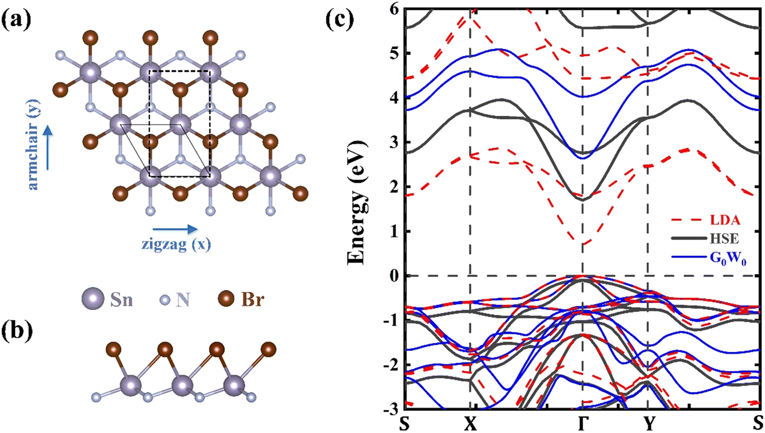 | ||
| Fig. 1 (a) Top view and (b) side view of the SnNBr monolayer – solid line rhombus represents hexagonal unit cell, dotted line rectangle represents orthorhombic unit cell. (c) Band dispersion of unstrained SnNBr monolayer; the solid blue, solid black and dashed red lines represent band dispersion calculated by G0W0, HSE06 and LDA, respectively. | ||
The difference in bandwidth of the highest valence band (HVB) and the lowest conduction band (LCB) is due to strong hybridization of Br (s + pz orbitals ∼2 + 15 = 17%), N (s + pz orbitals ∼24 + 6 = 30%), and Sn (s + pz orbitals ∼49 + 3 = 52%) orbitals in LCB. Whereas the HVB is composed mostly of only Br atom (px + py orbitals ∼70 + 27 = 97%), keeping the band localized and therefore nearly flat. The valence band maximum (VBM) is shared by a heavy hole band (HHB) and a light hole band (LHB), which is a characteristic of a typical semiconducting material. The orbital contributions of each element are shown in Fig. 2. Stronger orbital overlap due to hybridization in LCB creates more delocalized electronic states, leading to a more spread-out distribution of electrons, translating into the observed valley shape of the band.
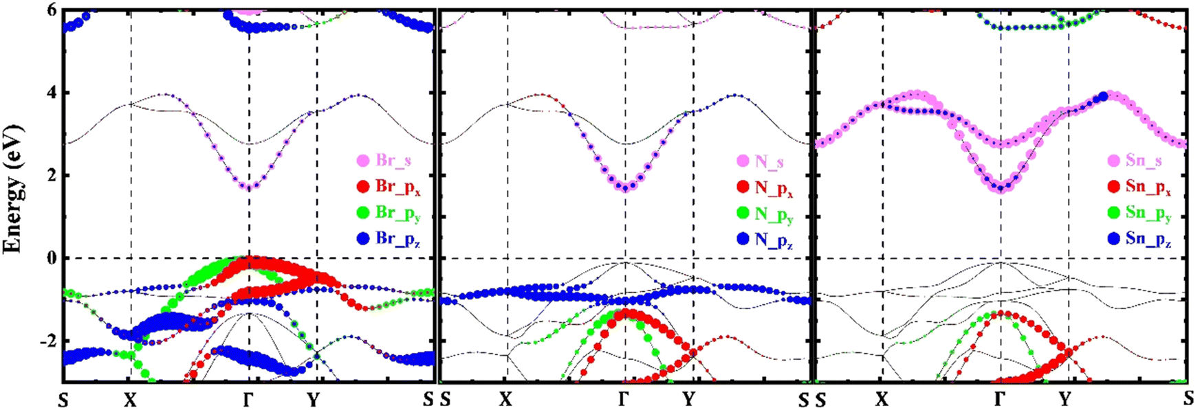 | ||
| Fig. 2 Major orbital contribution of Br, N and Sn atoms in the band dispersion of unstrained SnNBr monolayer. | ||
Strain can modify the band structure of the material, bringing the conduction and valence bands closer together. To meticulously understand the effect of strain on band dispersion, we focus on examining the isolated band dispersion of just HVB and LCB (Fig. 3(a)) in an orthorhombic unit cell. The Kronig–Penney model predicts a significant influence of strain on bandwidth,46 this effect has also been demonstrated in other materials previously.23,47 The bandwidth of LCB increases with the application of in-plane uniform biaxial tensile strain, effectively pushing the conduction band minima (CBM) to lower energy. Conversely, the bandwidth of the HVB narrows with tensile strain, resulting in a flatter HVB. Notably, while the CBM shifts downward, the valence band maxima (VBM) remain nearly at the same energy level, leading to a reduction in the electronic band gap. Interestingly, the position of the CBM and VBM is insensitive to strain and remains at Γ under ±4% biaxial strain, keeping the band gap direct. Furthermore, the bandwidth of both the HH and LH valence bands is decreasing under the effect of tensile strain, as visible in Fig. 3(b). We have also conducted these studies using a hexagonal unit cell and found results identical to those of the orthorhombic unit cell, as shown in the comparative results in Fig. S2 in the ESI.† The energy gap between the HH and LH valence bands increases from 1.2 meV to 4.5 meV under the effect of strain, making the HHB or the nearly flat band as the HVB invariably. The observed discrepancy in the strain response between the LCB and HVB can be attributed to the underlying mechanisms of band formation. In order to scrutinize it closely, we investigated the effect of strain on the orbital composition of LCB and HVB, as shown in Fig. 4.
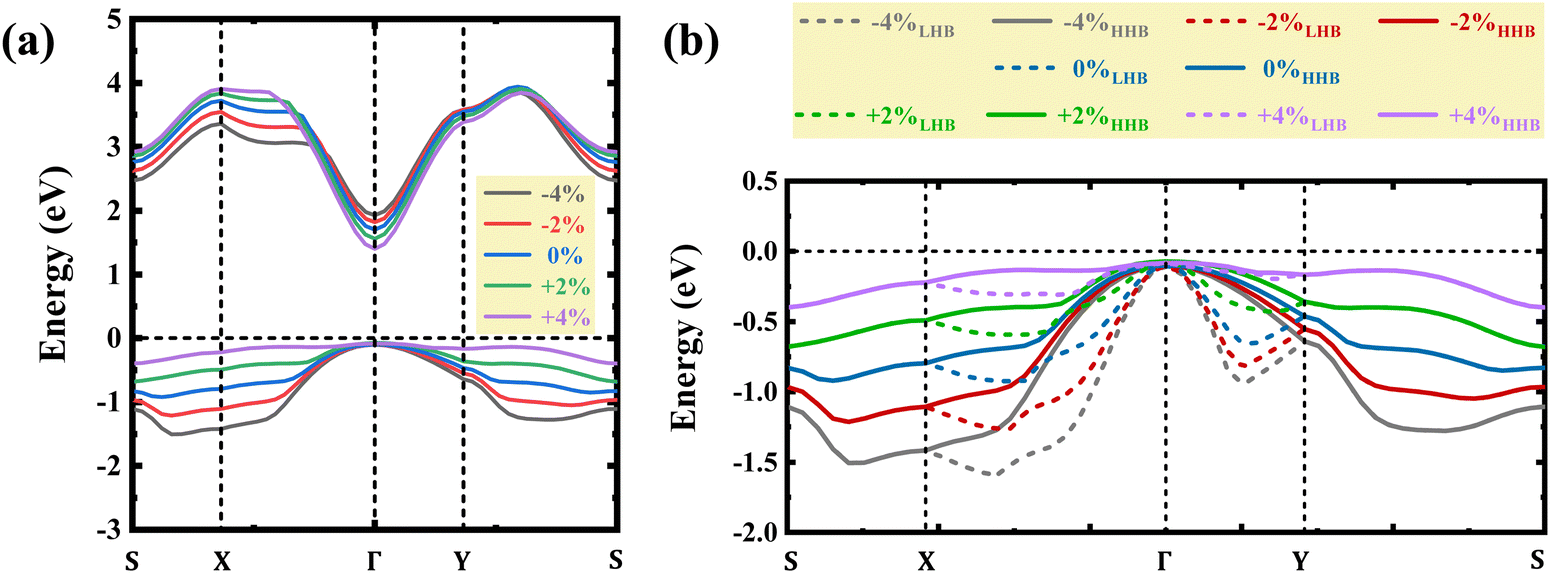 | ||
| Fig. 3 (a) Effect of strain on the lowest conduction band (LCB) and highest valence band (HVB), (b) light hole band (LHB) (dashed lines) and heavy hole band (HHB) (solid lines) under the effect of strain; compressive strain is represented by negative sign, and tensile strain is represented by positive sign. | ||
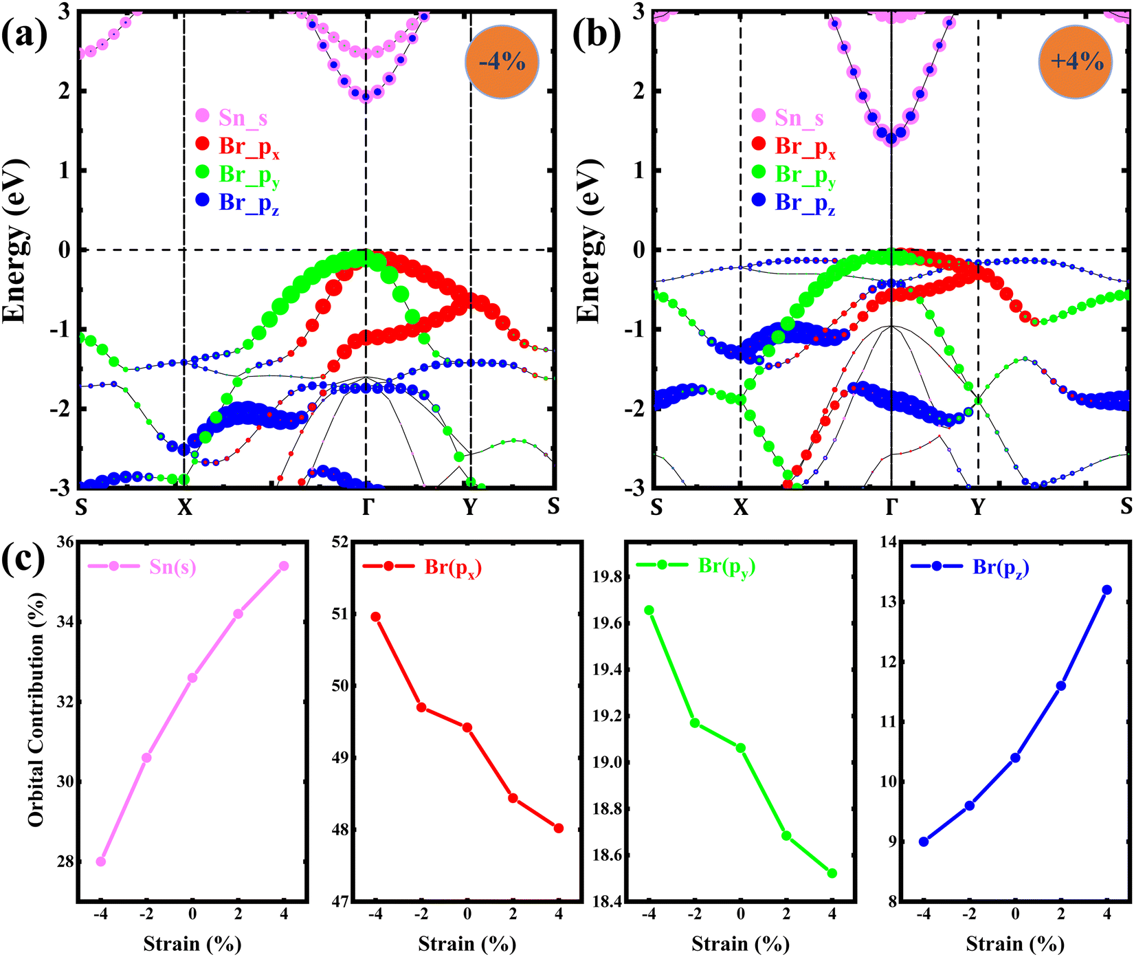 | ||
| Fig. 4 Orbital contributions in the SnNBr monolayer (a) compressed to 4% and (b) stretched to 4%. (c) Variation of the Sn_s, Br_px, Br_py, and Br_pz orbital contribution under the effect of strain. | ||
When tensile strain is applied to a material, the lattice spacing increases. This change in the atomic structure affects the orbital contributions to the electronic bands near the band edges. The strain alters the crystal field splitting and the overlap between the atomic orbitals, leading to a modification of the band structure near the band edges. To understand this behaviour, we further analyse the contribution of Sn_s, Br_px, Br_py, and Br_pz orbitals, as shown in Fig. 4(c). The contribution of Br_px and Br_py orbitals in the HVB is decreasing under tensile strain. The contributions by Br_pz orbitals move close to the top of the valence band with tensile strain (Fig. 4(b)) and away under compressive strain (Fig. 4(a)), resulting in a tuneable bandwidth for the HVB under the effect of strain. Conversely, the increased hybridization of Sn_s and Br_py orbitals under the effect of tensile strain conceivably causes the increase in the bandwidth of LCB, making it more delocalized. When atomic orbitals hybridize, the overlap of atomic orbitals can lead to stronger interactions between atoms, creating a larger number of available energy levels, which can widen the energy range of the band.
For a comprehensive comparison, we further calculated the G0W0 quasi-particle band gap and BSE optical band gap under the effect of strain. The variation of the band gap with strain is shown in Fig. 5(a). Both the electronic and optical band gap are decreasing under tensile strain, consistent with the above analysis. The difference between these, Eb = Eqp − Eop, represents the exciton binding energy of the first bright exciton. Both the optical and electronic gap decrease under strain, though this decrease is non-monotonic, resulting in a tuneable but inconsistent trend in the exciton binding energy. The decrease/increase in bandwidth (W) of HVB/LCB is calculated by the G0W0 quasi particle calculations, as shown in Fig. 5(b). Under the influence of strain, the bandwidth of HVB narrows significantly from 1.28 eV (at 4% compressive strain) to 0.23 eV (at 4% tensile strain), while that of LCB expands from 1.88 eV (at 4% compressive strain) to 2.35 eV (at 4% tensile strain). Having the advantage of the localized highest valence band, a good number of optical transitions are expected with fast decay rate. Fig. 5(c) reports optical spectra of the unstrained SnNBr monolayer obtained via G0W0 + BSE, along with the oscillator strength of optical transitions. Evidently, a significant number of bright excitons are observed in the visible region (1.63–3.26 eV) and a continuum of dark excitons is available at higher energies.
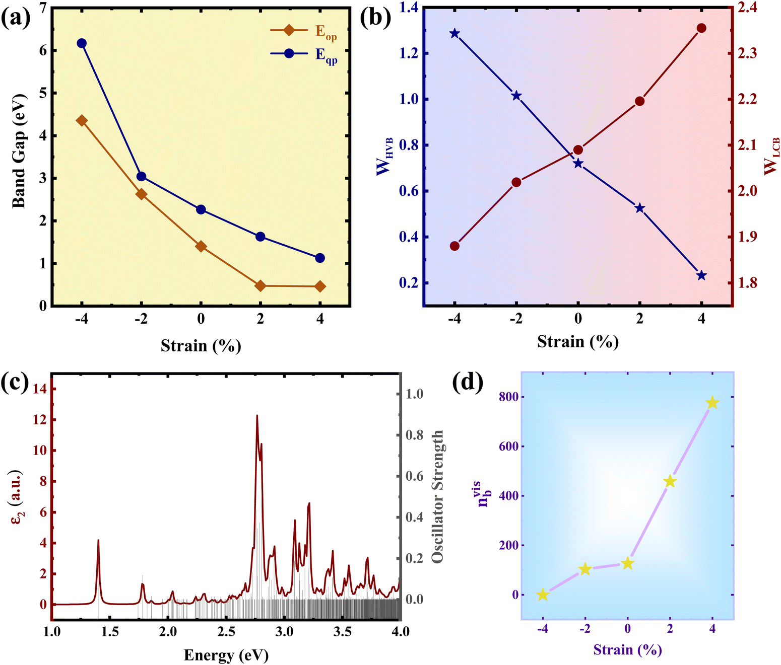 | ||
| Fig. 5 (a) Optical (Eop) and quasi-particle (Eqp) band gap decreasing with increase in strain, (b) bandwidth of highest valence band (HVB) and lowest conduction band (LCB) under the effect of strain, (c) optical spectra of unstrained SnNBr using G0W0 + BSE, and (d) increasing population of bright excitons under the effect of strain. | ||
Furthermore, we take the ensemble of only bright excitons in the visible energy range under the effect of strain. The population of bright excitons increases drastically with the application of tensile strain, as can be seen in Fig. 5(d). This can be viewed as a chief advantage of having a flat band in semiconducting materials. The flatter the HVB gets, the higher the number of optical transitions.
Fig. 6(a) and (b) display the absorption spectra and solar flux of the SnNBr monolayer under the effect of strain, as calculated by G0W0 + BSE. The results indicate a noticeable red shift in the absorption spectra and solar flux, showing an increase in the number of optical transitions in the visible region. Abundant availability of bright excitons indicates excellent absorption and suits SnNBr monolayer to optoelectronic properties. The bright excitons have high oscillator strength and also high recombination rate.
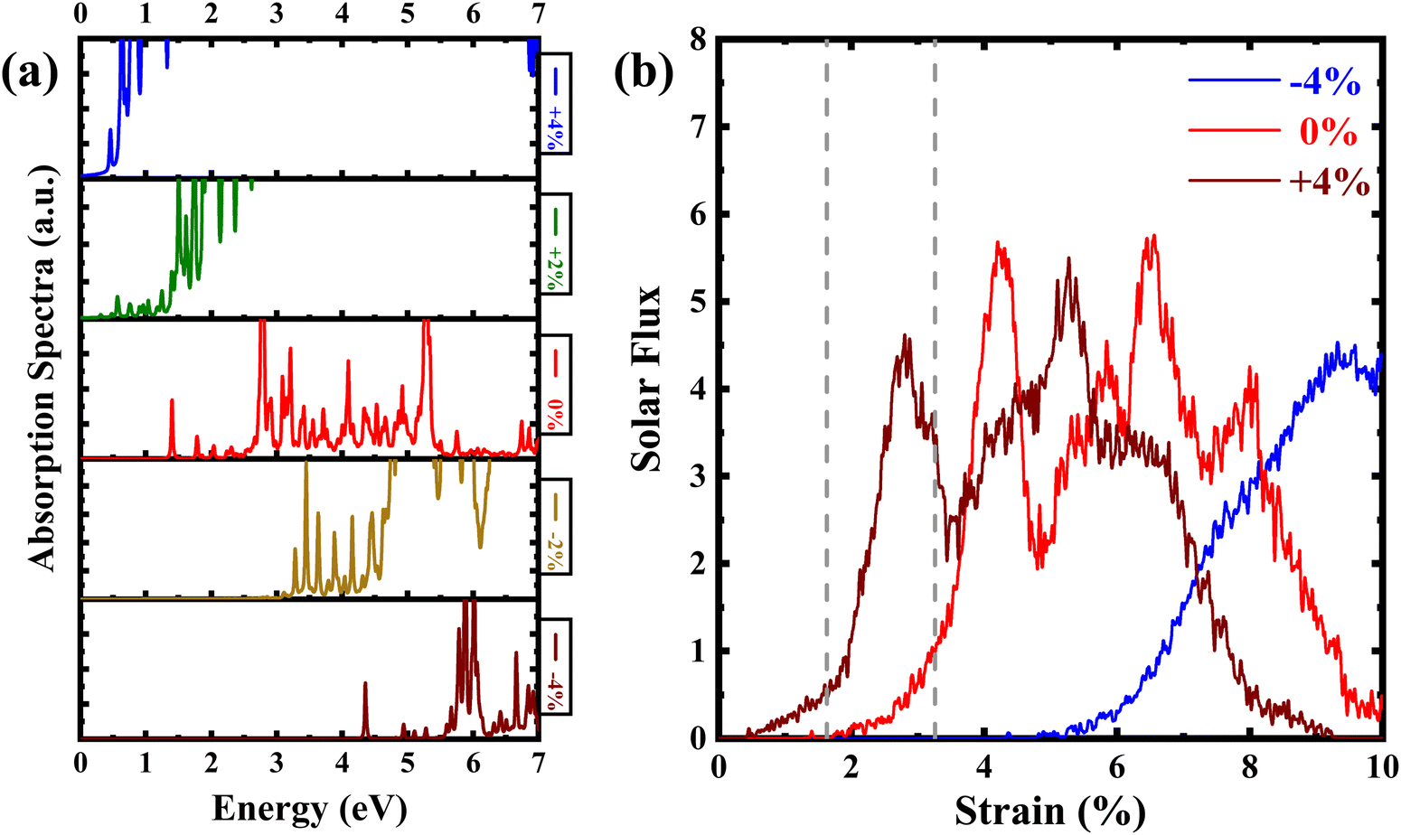 | ||
| Fig. 6 (a) Absorption spectra of SnNBr showing red shift under the effect of tensile strain, and (b) solar flux of SnNBr shifting prominently in the visible region with increasing strain. | ||
Increased orbital overlap resulting from hybridization in LCB leads to more delocalized (spread out) orbitals, which in turn reduces the effective mass of electrons  under tensile strain. In contrast, the more localized and flatter HVB have a higher effective hole mass
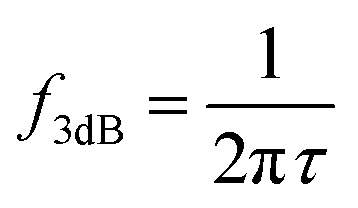
  when tensile strain is applied, as shown in Fig. 7(a). The effective mass of an electron remains isotropic under the effect of strain along both armchair and zigzag directions, while that of the hole tends to be anisotropic with tensile strain, which can also be observed by the curvature of the highest valence band, clearly visible in Fig. 3 and Fig. 4. Furthermore, the reduced band gap under the effect of tensile strain increases the overlap of their wavefunctions, enhancing the probability of radiative recombination, both along the armchair and zigzag directions, as shown in Fig. 7(b). The average radiative recombination rate and exciton radiative lifetime are calculated at zero momentum using the Wannier approach with Fermi's golden rule.48 This approach is effectively used in many recent studies.22,49–51 Details of the formalism are given in the ESI.† High radiative recombination rate leads to more efficient conversion of electrical energy into light energy in laser diodes. This improves the overall efficiency and brightness of the laser device.52,53 No difference is observed in the recombination rates of the unstrained SnNBr monolayer along the armchair and zigzag directions, which is consistent with the isotropic nature of the SnNBr monolayer.14 Minute anisotropy arises on the application of strain. Exciton radiative lifetime at zero momentum (k = 0) is taken as the inverse of the radiative recombination rate. Notably, the short lifespan of excitons can enhance the internal quantum efficiency and support telecommunications applications.54,55 With increasing tensile strain, HVB becomes flatter; maximizing the overlap of the wave functions and significantly enhancing the transition probability. As a result, the lifetime of the carrier is greatly reduced (Fig. 7(b)). Recent research has shown that the carrier recombination lifetime has a more significant impact on the modulation bandwidth of the visible light communication (VLC) system than the RC (resistance–capacitance) time delay and doping concentration.32,56 The modulation bandwidth is the frequency range over which a device can effectively modulate signals. It is particularly important in applications like optical communications, where the ability to transmit data at high speeds is essential. The f3dB point indicates the frequency at which the output power drops to half its maximum value or the voltage gain is attenuated to 0.707, the value at the peak, reflecting the device's capability to handle high-frequency signals. The LED modulation bandwidth is a limiting factor for ultra-high speed VLC systems,57,58 which is linked to the carrier recombination lifetime by the following equation at −3 dB scale:
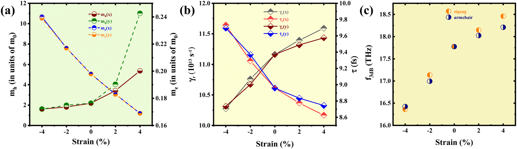 | ||
| Fig. 7 Effect of strain on: (a) effective hole mass (mh) and effective electron mass (me), (b) recombination rate (γr) and lifetime (τ) at zero momenta, and (c) modulation bandwidth at 3 dB-down scale (f3dB). | ||
This high value can be attributed to the nearly flat HVB, which is further confirmed by understanding the impact of strain on the modulation bandwidth. The modulation bandwidth can be tuned by the application of strain. The dependence of 3 dB-down modulation bandwidth (f3dB) on strain is shown in Fig. 7(c). Similar to all other factors, tensile strain causes minute anisotropy to the modulation bandwidth as well, which means that the modulation bandwidth can vary based on the orientation of the device relative to the applied electric field or the direction of light propagation. The orientation-dependent modulation bandwidth is beneficial for the design and optimization of high-speed LED devices.6
IV. Conclusion
This study demonstrates the potential for significant band engineering in semiconductors through strain-induced localization and delocalization of electronic states. It is shown that applying strain to the SnNBr monolayer flattens the highest valence band, thereby exhibiting excellent absorption properties in the visible spectrum, further improved by tensile strain due to an increased population of bright excitons. Notably, the effective hole mass is substantially increased, leading to a significant boost in radiative recombination rate and a corresponding reduction in lifetime. These combined effects enable the SnNBr monolayer, with its direct bandgap and nearly flat HVB, to achieve remarkably high modulation bandwidths on the order of terahertz. The results suggest that SnNBr-based LEDs hold immense promise for addressing the growing demand for high-speed data transmission, paving the way for advanced VLC systems to handle large volumes of data.Data availability
The data that support the findings of this study are available from the authors upon reasonable request.Conflicts of interest
The authors have no conflicts to disclose.Acknowledgements
The authors extend their heartfelt gratitude to the Institute of Nano Science and Technology (INST) in Mohali, PARAM-Smriti at NABI, Mohali and C-DAC in Pune for providing the supercomputing resources under the umbrella of the National Supercomputing Mission, by the Government of India. Additionally, the authors are deeply thankful for the fellowship and financial assistance provided by INST Mohali and the Council of Scientific and Industrial Research (CSIR), India, under grant number 09/1129(0030)/2020-EMR-I. Support from Project No. CRG/2023/001896 of Science and Engineering Research Board – Department of Science & Technology (SERB-DST), Govt. of India is gratefully acknowledged.References
- S. E. El-Khamy, in 2006 International Conference on Computer Engineering and Systems, ICCES’06, 2006, pp. 1–2.
- E. Oyekanlu, K. Scoles and P. O. Oladele, in 2018 10th International Conference on Advanced Infocomm Technology, ICAIT 2018, Institute of Electrical and Electronics Engineers Inc., 2018, pp. 93–101.
- Y. Zhu, X. Sun, Y. Tang, L. Fu and Y. Lu, Two-dimensional materials for light emitting applications: Achievement, challenge and future perspectives, Nano Res., 2021, 14, 1912–1936 CrossRef.
- K. J. Singh, W.-T. Huang, F.-H. Hsiao, W.-C. Miao, T.-Y. Lee, Y.-H. Pai and H.-C. Kuo, Recent Advances in Micro-LEDs Having Yellow–Green to Red Emission Wavelengths for Visible Light Communications, Micromachines, 2023, 14, 478 CrossRef PubMed.
- R. Wan, L. Wang, J. Huang, X. Yi, H.-C. Kuo and J. Li, Improving the Modulation Bandwidth of GaN-Based Light-Emitting Diodes for High-Speed Visible Light Communication: Countermeasures and Challenges, Adv. Photon. Res., 2021, 2, 2100093 CrossRef.
- M. Monavarian, A. Rashidi, A. A. Aragon, S. H. Oh, A. K. Rishinaramangalam, S. P. Denbaars and D. Feezell, Impact of crystal orientation on the modulation bandwidth of InGaN/GaN light-emitting diodes, Appl. Phys. Lett., 2018, 112, 41104 CrossRef.
- D. Tsonev, H. Chun, S. Rajbhandari, J. J. D. McKendry, S. Videv, E. Gu, M. Haji, S. Watson, A. E. Kelly, G. Faulkner, M. D. Dawson, H. Haas and D. O’Brien, A 3-Gb/s single-LED OFDM-based wireless VLC link using a gallium nitride μ LED, IEEE Photonics Technol. Lett., 2014, 26, 637–640 Search PubMed.
- X. Liu, H. Chen, S. Liang, M. Zhang, Z. Jiang, S. Fan and Y. Sun, Ultrabroadband electrically controllable terahertz modulation based on GaAs Schottky diode structure, AIP Adv., 2021, 6(11), 111301 Search PubMed.
- H. Zeng, S. Gong, L. Wang, K. Ding, H. Liang, F. Lan, T. Zhou, S. Liang, W. Wang, Y. Gong, Z. Yang, T. J. Cui and Y. Zhang, High-Speed Modulations of Guided Terahertz Waves via 2DEG Tiny Metasurfaces, Laser Photon. Rev., 2023, 17, 2300122 CrossRef.
- T. Brumme, M. Calandra and F. Mauri, Electrochemical doping of few-layer ZrNCl from first principles: Electronic and structural properties in field-effect configuration, Phys. Rev. B: Condens. Matter Mater. Phys., 2014, 89, 245406 CrossRef.
- L. Zárate-Aldava and A. R. Botello-Méndez, Charge doping zirconium nitride halide monolayers, Chem. Phys. Lett., 2022, 786, 139128 CrossRef.
- J. T. Ye, S. Inoue, K. Kobayashi, Y. Kasahara, H. T. Yuan, H. Shimotani and Y. Iwasa, Liquid-gated interface superconductivity on an atomically flat film, Nat. Mater., 2009, 9, 125–128 CrossRef PubMed.
- S. Zhang, M. Tanaka, H. Zhu and S. Yamanaka, Superconductivity of layered β-HfNCl with varying electron-doping concentrations and interlayer spacings, Supercond. Sci. Technol., 2013, 26, 085015 CrossRef.
- P. Nandi and A. De Sarkar, DFT Insights into Layer-Dependent Superhigh Piezoelectricity and Carrier Mobility in 2D Hexagonal SnNBr, J. Phys. Chem. C, 2023, 127, 23551–23565 CrossRef.
- P. Nandi and S. Sharma, and A. De Sarkar, Intrinsic spin Hall and Rashba effects in metal nitride bromide monolayer for spin-orbitronics, J. Appl. Phys., 2024, 135(23), 234302 CrossRef.
- W. Wu, C. Pan, Y. Zhang, X. Wen and Z. L. Wang, Piezotronics and piezo-phototronics – From single nanodevices to array of devices and then to integrated functional system, Nano Today, 2013, 8, 619–642 CrossRef.
- Z. L. Wang and W. Wu, Piezotronics and piezo-phototronics: fundamentals and applications, Natl. Sci. Rev., 2014, 1, 62–90 CrossRef.
- T. Uematsu, J. Kimura and Y. Yamaguchi, The reversible photoluminescence enhancement of a CdSe/ZnS nanocrystal thinfilm, Nanotechnology, 2004, 15, 822 CrossRef.
- X. Wang, H. Zhang, R. Yu, L. Dong, D. Peng, A. Zhang, Y. Zhang, H. Liu, C. Pan, Z. Lin Wang, X. Wang, H. Zhang, L. Dong, D. Peng, A. Zhang, Y. Zhang, H. Liu, C. Pan, Z. L. Wang and R. Yu, Dynamic Pressure Mapping of Personalized Handwriting by a Flexible Sensor Matrix Based on the Mechanoluminescence Process, Adv. Mater., 2015, 27, 2324–2331 CrossRef PubMed.
- C. Du, C. Jiang, P. Zuo, X. Huang, X. Pu, Z. Zhao, Y. Zhou, L. Li, H. Chen, W. Hu and Z. L. Wang, Piezo-Phototronic Effect Controlled Dual-Channel Visible light Communication (PVLC) Using InGaN/GaN Multiquantum Well Nanopillars, Small, 2015, 11, 6071–6077 CrossRef PubMed.
- Y. Xing, Q. Chaudry, C. Shen, K. Y. Kong, H. E. Zhau, L. W. Chung, J. A. Petros, R. M. O’Regan, M. V. Yezhelyev, J. W. Simons, M. D. Wang and S. Nie, Bioconjugated quantum dots for multiplexed and quantitative immunohistochemistry, Nat. Protoc., 2007, 2, 1152–1165 CrossRef PubMed.
- H. Seksaria, A. Kaur, K. Singh and A. De Sarkar, Hexagonal and tetragonal ScX (X = P, As, Sb) nanosheets for optoelectronics and straintronics, Appl. Surf. Sci., 2023, 615, 156306 CrossRef.
- H. Seksaria, A. Kaur and A. De Sarkar, Origin of strain tunability in flat valence band and ultrahigh shear piezoelectricity in superflexible non-van der Waals graphitic ScX monolayers (X= P, As, Sb), Phys. Rev. B, 2023, 108, 075426 CrossRef.
- M. Hosseini, M. Elahi, M. Pourfath and D. Esseni, Very large strain gauges based on single layer MoSe2 and WSe2 for sensing applications, Appl. Phys. Lett., 2015, 107(25), 253503 CrossRef.
- C. E. P. Villegas and A. R. Rocha, Elucidating the optical properties of novel heterolayered materials based on MoTe2-InN for photovoltaic applications, J. Phys. Chem. C, 2015, 119, 11886–11895 CrossRef.
- M. A. U. Absor, H. Kotaka, F. Ishii and M. Saito, Strain-controlled spin splitting in the conduction band of monolayer WS2, Phys. Rev. B, 2016, 94, 115131 CrossRef.
- H. Shu and J. Guo, Enhanced stability and tunable optoelectronic properties of silicon–carbon monolayers by strain and surface functionalization, J. Mater. Chem. C, 2024, 12, 5916–5925 RSC.
- H. Shu and J. Guo, Strain effects of stability, transport, and electro-optical properties of novel Ga2TeS monolayer, J. Mater. Sci., 2024, 59, 2403–2415 CrossRef.
- H. Shu, Adjustable electro-optical properties of novel graphene-like SiC2 via strain engineering, Appl. Surf. Sci., 2021, 559, 149956 CrossRef.
- A. Reale, G. Massari, A. Di Carlo, P. Lugli, A. Vinattieri, D. Alderighi, M. Colocci, F. Semond, N. Grandjean and J. Massies, Comprehensive description of the dynamical screening of the internal electric fields of AlGaN/GaN quantum wells in time-resolved photoluminescence experiments, J. Appl. Phys., 2003, 93, 400–409 CrossRef.
- P. Krogstrup, H. I. Jørgensen, M. Heiss, O. Demichel, J. V. Holm, M. Aagesen, J. Nygard and A. Fontcuberta i Morral, Single-nanowire solar cells beyond the Shockley–Queisser limit, Nat. Photonics, 2013, 7, 306–310 CrossRef.
- J. Heinen, W. Harth and W. Huber, Frequency Response of GaAIAs Light-Emitting Diodes, IEEE Trans. Electron Devices, 1976, 23, 478–480 Search PubMed.
- P. Hohenberg and W. Kohn, Inhomogeneous electron gas, Phys. Rev., 1964, 136, B864 CrossRef.
- G. Kresse and J. Furthmüller, Efficiency of ab-initio total energy calculations for metals and semiconductors using a plane-wave basis set, Comput. Mater. Sci., 1996, 6, 15–50 CrossRef.
- G. Kresse and J. Furthmüller, Efficient iterative schemes for ab initio total-energy calculations using a plane-wave basis set, Phys. Rev. B: Condens. Matter Mater. Phys., 1996, 54, 11169 CrossRef PubMed.
- G. Kresse and D. Joubert, From ultrasoft pseudopotentials to the projector augmented-wave method, Phys. Rev. B: Condens. Matter Mater. Phys., 1999, 59, 1758 CrossRef.
- J. P. Perdew, K. Burke and M. Ernzerhof, Generalized Gradient Approximation Made Simple, Phys. Rev. Lett., 1996, 77, 3865 CrossRef.
- A. V. Krukau, O. A. Vydrov, A. F. Izmaylov and G. E. Scuseria, Influence of the exchange screening parameter on the performance of screened hybrid functionals, J. Chem. Phys., 2006, 125, 224106 CrossRef PubMed.
- P. Giannozzi, S. Baroni, N. Bonini, M. Calandra, R. Car, C. Cavazzoni, D. Ceresoli, G. L. Chiarotti, M. Cococcioni and I. Dabo, et al., QUANTUM ESPRESSO: a modular and open-source software project for quantum simulations of materials, J. Phys.: Condens. Matter, 2009, 21, 395502 CrossRef.
- D. R. Hamann, M. Schlüter and C. Chiang, Norm-Conserving Pseudopotentials, Phys. Rev. Lett., 1979, 43, 1494 CrossRef.
- D. R. Hamann, Optimized norm-conserving Vanderbilt pseudopotentials, Phys. Rev. B, 2013, 88, 085117 CrossRef.
- A. F. Starace, Length and Velocity Formulas in Approximate Oscillator-Strength Calculations, Phys. Rev. A, 1971, 3, 1242 CrossRef.
- D. Sangalli, A. Ferretti, H. Miranda, C. Attaccalite, I. Marri, E. Cannuccia, P. Melo, M. Marsili, F. Paleari and A. Marrazzo, et al., Many-body perturbation theory calculations using the yambo code, J. Phys.: Condens. Matter, 2019, 31, 325902 CrossRef.
- A. Marini, C. Hogan, M. Grüning and D. Varsano, yambo: An ab initio tool for excited state calculations, Comput. Phys. Commun., 2009, 180, 1392–1403 CrossRef.
- G. K. H. Madsen and D. J. Singh, BoltzTraP. A code for calculating band-structure dependent quantities, Comput. Phys. Commun., 2006, 175, 67–71 CrossRef CAS.
- A. R. Beattie and P. Landsberg, One-dimensional overlap functions and their application to Auger recombination in semiconductors, Proc. R. Soc. London, Ser. A, 1960, 258, 486–495 CAS.
- S. Tao, X. Zhang, J. Zhu, P. He, S. A. Yang, Y. Lu and S. H. Wei, Designing Ultra-flat Bands in Twisted Bilayer Materials at Large Twist Angles: Theory and Application to Two-Dimensional Indium Selenide, J. Am. Chem. Soc., 2022, 144, 3949–3956 CrossRef CAS PubMed.
- J. William and N. H. March, Theoretical solid state physics (Interscience monographs and texts in physics and astronomy, v. 27), 1973 Search PubMed.
- M. Re Fiorentin, F. Risplendi, M. Palummo and G. Cicero, First-Principles Calculations of Exciton Radiative Lifetimes in Monolayer Graphitic Carbon Nitride Nanosheets: Implications for Photocatalysis, ACS Appl. Nano Mater., 2021, 4, 1985–1993 CrossRef CAS.
- Z. Yan, Y. Li and S. Wang, Spin Mixing Control of Interlayer Excitons in ZrS2/ZrNCl Heterostructures, J. Phys. Chem. C, 2023, 127, 20939–20944 CrossRef CAS.
- H. Seksaria, A. Kishore and A. De Sarkar, Temperature-driven journey of dark excitons to efficient photocatalytic water splitting in β-AsP, Phys. Chem. Chem. Phys., 2024, 26(35), 22882–22893 RSC.
- C. Jia, C. He, Z. Liang and Q. Wang, Improvement of Radiative Recombination Rate and Efficiency Droop of InGaN Light Emitting Diodes with In-Component-Graded InGaN Barrier, Phys. Status Solidi, 2021, 218, 2100351 CrossRef CAS.
- Y.-F. Wang, M. I. Niass, F. Wang and Y.-H. Liu, Improvement of radiative recombination rate in deep ultraviolet laser diodes with step-like quantum barrier and aluminum-content graded electron blocking layer, Chin. Phys. B, 2020, 29, 017301 CrossRef CAS.
- M. M. Emara, S. J. Burya and P. G. Van Patten, Enhancement of biexciton generation via resonance energy transfer in nanoclusters of colloidal CdTe quantum dots for optical gain applications, Mater. Chem. Phys., 2022, 277, 125540 CrossRef CAS.
- L. Shi, C. K. Lee and A. P. Willard, The Enhancement of Interfacial Exciton Dissociation by Energetic Disorder Is a Nonequilibrium Effect, ACS Cent. Sci., 2017, 3, 1262–1270 CrossRef CAS PubMed.
- C. Du, X. Huang, C. Jiang, X. Pu, Z. Zhao, L. Jing, W. Hu and Z. L. Wang, Tuning carrier lifetime in InGaN/GaN LEDs via strain compensation for high-speed visible light communication, Sci. Rep., 2016, 6, 1–10 CrossRef PubMed.
- C. W. Chow, C. H. Yeh, Y. F. Liu and Y. Liu, Improved modulation speed of LED visible light communication system integrated to main electricity network, Electron. Lett., 2011, 47, 867–868 CrossRef.
- C.-H. Yeh, Y.-L. Liu, C.-W. Chow, C. H. Yeh, C. W. Chow, Y. F. Liu, P. Y. Huang, H. Le Minh, G. Faulkner, L. Zeng, K. Lee, D. Jung, Y. Oh, Y. Liu, Y. L. Liu, H. K. Tsang, D. Langer and J. W. Walewski, Real-time white-light phosphor-LED visible light communication (VLC) with compact size, Opt. Express, 2013, 21, 26192–26197 CrossRef.
Footnotes |
| † Electronic supplementary information (ESI) available. See DOI: https://doi.org/10.1039/d4cp03829k |
| ‡ Both of these authors contributed equally. |
| This journal is © the Owner Societies 2025 |