
Ferroelastic phase transition-modulated electronic transport and photoelectric properties in monolayer 1T′ ZrCl2†
Yuehua
Xu
 *,
He
Sun
,
Jindian
Chen
,
Qianqian
Long
and
Haowen
Xu
*,
He
Sun
,
Jindian
Chen
,
Qianqian
Long
and
Haowen
Xu
School of Microelectronics and Control Engineering, Changzhou University, Changzhou 213164, Jiangsu, China. E-mail: yhxu@cczu.edu.cn
First published on 17th December 2024
Abstract
Monolayer 1T′ ZrCl2 exhibits unique ferroelastic behavior with three structurally distinct variants (O1, O2, and O3), demonstrating potential for next-generation nanoelectronic and optoelectronic devices. This study investigates the electronic transport and optoelectronic properties of the O1 and O3 variants, with O3 serving as a representative for both O2 and O3 due to their structural symmetry. First-principles calculations and non-equilibrium Green's function analysis reveal that the O1 variant possesses exceptional electronic properties, including high electron mobility (1.44 × 104 cm2 V−1 s−1) and a large current on/off ratio (106), while the O3 variant shows high conductivity in both crystallographic directions. Optoelectronically, the O1 variant demonstrates strong anisotropy with a maximum photocurrent density of 6.57 µA mm−2, photo responsivity of 0.37 A W−1, and external quantum efficiency of 41.08% along the a direction, outperforming many 2D materials, whereas there is negligible response along the b direction. In contrast, the O3 variant exhibits a more balanced photoresponse with comparable performance in both directions. These findings provide insights into structure–property relationships in ferroelastic 2D materials and pave the way for developing phase transition-based multifunctional devices for applications in information processing, energy conversion, and sensing.
1 Introduction
Research on two-dimensional (2D) materials has advanced considerably over the past two decades. These ultra-thin substances exhibit distinctive physical, chemical, and electronic properties compared to their bulk counterparts, thereby laying the foundation for the next generation of nanoelectronic and optoelectronic devices.1–8 Within this diverse family of materials, transition metal dichalcogenides (TMDs) have attracted significant attention, with group VIB TMDs (e.g., MoS2, WS2) featuring layer-dependent direct bandgaps, strong light–matter interactions, and high on/off ratios for electronic and optoelectronic applications,9–15 while group IVB TMDs (e.g., ZrS2, ZrSe2) exhibit exceptional carrier mobilities exceeding 2 × 103 cm2 V−1 s−1,16 and their nitrogen-based analogues (e.g., Zr2N3H) show promise for visible-light photocatalysis.17 2D metal halides such as CuI and BiI3 demonstrate unique properties including high photosensitivity and tunable bandgaps.18–21 Halide-based materials have further emerged as a pivotal platform for studying magnetism at the atomic scale, exemplified by CrI3 as the first reported 2D ferromagnet with strong perpendicular magnetic anisotropy and CrBr3 with similar properties but lower Curie temperatures.22 Recent computational studies have further expanded this family by discovering promising halide-based materials including MeX2/MeXY transition metal halides (e.g., CdI2, ZnClI) for efficient photocatalysis and ternary alkaline-earth metal chlorides (e.g., CaSn2Cl6, CaPb2Cl6) as potential p-type transparent conductors, enriching the toolbox for fundamental physics exploration and device engineering at the atomic scale.23,24In recent years, the discovery of ferroic orders in 2D materials has opened up new avenues for next-generation multifunctional nanoelectronic and optoelectronic device applications.25–27 One such class of materials that has emerged as a promising candidate is 2D ferroelastic materials, characterized by the presence of two or more orientation states that can be switched by applied mechanical stress. This phenomenon has been observed in several 2D materials, including 1T′-TMDs (MX2, where X = S, Se, Te and M = Mo, W, Re),28 phosphorene and its analogs (GeS, GeSe, SnS, SnSe),29,30 honeycomb monolayers (graphene, BN, stanene),31 silver(II) fluoride (AgF2),32 chromium dihalide (CrI2),33 β′-In2Se3,34 and 2D perovskites (2L or thicker).35 Their unique mechanical switching capability offers an additional degree of freedom for device engineering and functionality, making them promising candidates for future applications.
Recently, monolayer ZrCl2 in its ground-state 1T′ phase has emerged as a novel 2D ferroelastic material, exhibiting an unprecedented 120° lattice rotation ferroelasticity.36 This unique structural characteristic gives rise to three distinct ferroelastic variants (O1, O2, and O3), which fundamentally differ from the conventional 90° orthogonal transitions commonly observed in traditional ferroelastic systems.36 The coupling between this distinctive ferroelastic behavior and the material's predicted anisotropic electrical and optical absorption properties opens up intriguing possibilities for property control through ferroelastic switching. The structural asymmetry-driven ferroelastic transitions can potentially enable tunable electrical states and controllable optical responses, making monolayer ZrCl2 particularly promising for diverse applications, including programmable electronic devices, directional photodetectors, and other multifunctional instruments.28,34,37–43 However, while these initial findings are promising, a fundamental gap remains in our understanding of the collective influence of ferroelasticity and structural anisotropy on electronic transport and photocurrent characteristics.
To address the current research gap and unlock the potential of ZrCl2 in programmable nanoelectronic and optoelectronic devices, we present a comprehensive investigation of monolayer 1T′ phase ZrCl2, focusing on its carrier mobility, electronic transport properties, and photocurrent characteristics. Because O2 and O3 are rotated 120° relative to O1 and are mirror-symmetric to each other, our study focuses predominantly on the O1 variant, employing the O3 variant as a comparative reference to encompass all three variants effectively. Utilizing first-principles calculations and non-equilibrium Green's function theory, we aim to quantify the carrier mobility and electronic transport properties, characterize optoelectronic properties, and investigate the impact of ferroelastic phase transitions on these properties for both variants. By conducting this comprehensive study, we expect to bridge the gap between fundamental material science and practical device applications, potentially opening new avenues for programmable and adaptive nanoelectronic and optoelectronic technologies in fields such as information processing, energy conversion, and sensing.
2 Computational details
2.1 Calculational methods for the geometric and electronic structures of monolayer ZrCl2
The geometric optimization and electronic properties of the monolayer ZrCl2 were calculated using the QuantumATK (S-2021.06)44 software based on density functional theory (DFT).45 The Perdew–Burke–Ernzerhof (PBE) form of the generalized gradient approximation (GGA) and the linear combination of atomic orbitals (LCAO) methods were employed,46 with the all-electron potential replaced by the PseuDodojo pseudopotentials47 and a medium numerical basis for the wave function expansion. The real space density grid was truncated at 55 hartree, and a k-point grid density of 14 × 8 × 1 was utilized to sample the first Brillouin zone of ZrCl2. Structural optimization convergence was achieved when the maximum force on each atom fell below 0.01 eV Å−1. A vacuum spacing of 19 Å was implemented to prevent interlayer interactions. To comprehensively evaluate the electronic properties, calculations were performed both with and without spin–orbit coupling (SOC) effects. Since the SOC effects were found to be negligible on the electronic structure, subsequent calculations were conducted without SOC to optimize computational efficiency. For more precise bandgap results, the Heyd–Scuseria–Ernzerhof (HSE06) hybrid functional was employed.48 Stability assessment of monolayer ZrCl2 involved phonon spectrum calculations using an 11 × 9 × 1 supercell and ab initio molecular dynamics simulations with a 5 × 3 × 1 supercell. Molecular dynamics simulations were performed at 300 K using the NVT Nose–Hoover thermostat49,50 with a thermostat time scale of 100 fs and a time step of 1 fs.2.2 Calculational method of carrier mobility
The carrier mobility (μ) of 2D materials is evaluated using a modified formula within the framework of deformation potential (DP) theory.51 This model considers the anisotropy of the deformation potential, elastic constants, and effective mass, allowing for a more comprehensive description of the material's anisotropy. The formula for determining the carrier mobility of 2D materials is as follows: | (1) |
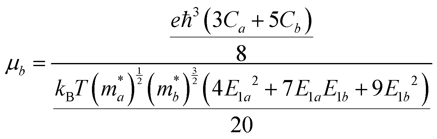 | (2) |
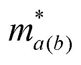 corresponds to the elastic constant, deformation potential and effective mass in a and b directions, respectively. The two-dimensional elastic modulus Ca(b) was directly computed using the QuantumATK software. By linearly fitting the conduction band minimum (CBM) and valence band maximum (VBM) as a function of strain, we obtained E1a(b). The effective mass
  at the CBM and VBM was calculated using the finite-difference (FD) representation of the E(k) derivative. This method was chosen for its superior accuracy compared to simple parabolic band fitting, especially for complex band structures.
2.3 Calculational method of I–V characteristics curve
The carrier transport was calculated by combining nonequilibrium Green's function (NEGF) and DFT methods.52,53 Again, the PBE functional with LCAO methods and PseuDodojo pseudopotentials were employed for calculating carrier transport. The I–V characteristic curve calculations involved setting the Brillouin zone to 94 × 5 × 1 k-meshes and 8 × 151 × 1 k-meshes along the a and b directions, respectively. The I–V characteristics of the two-probe systems were then derived using the Landauer–Büttiker formalism:54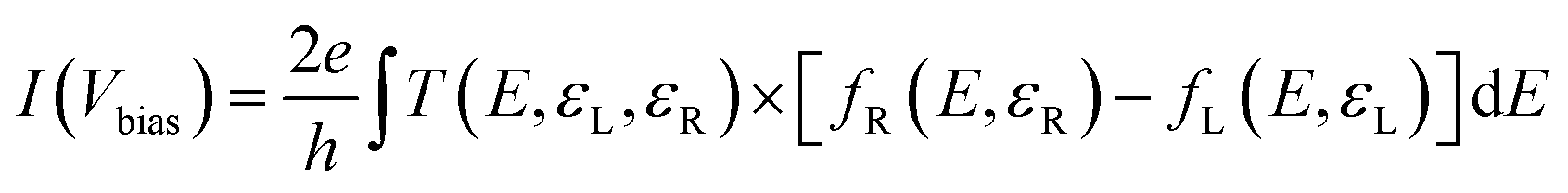 | (3) |
2.4 Calculational method of photocurrent
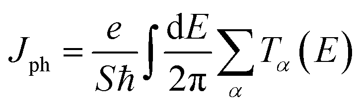
Calculation of the photocurrent density Jph involved integrating the NEGF methodology within the first-order perturbation theory framework, based on the first Born approximation.55,56 The perturbation resulting from electron–light interaction is defined by a Hamiltonian, represented as: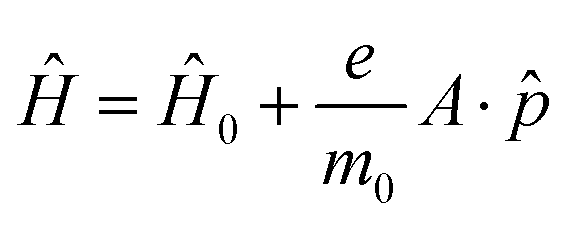 | (4) |
![[p with combining circumflex]](https://www.rsc.org/images/entities/i_char_0070_0302.gif) denotes the momentum operator, and A is the electromagnetic vector potential. Transmission coefficients were calculated as:57
denotes the momentum operator, and A is the electromagnetic vector potential. Transmission coefficients were calculated as:57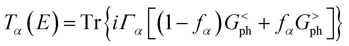 | (5) |
 | (6) |
In addition, the functional, basis, pseudopotentials and k-meshes used in photocurrent calculations are consistent with those employed in carrier transport simulations.
3 Results and discussion
3.1 Structural and electronic properties of ZrCl2
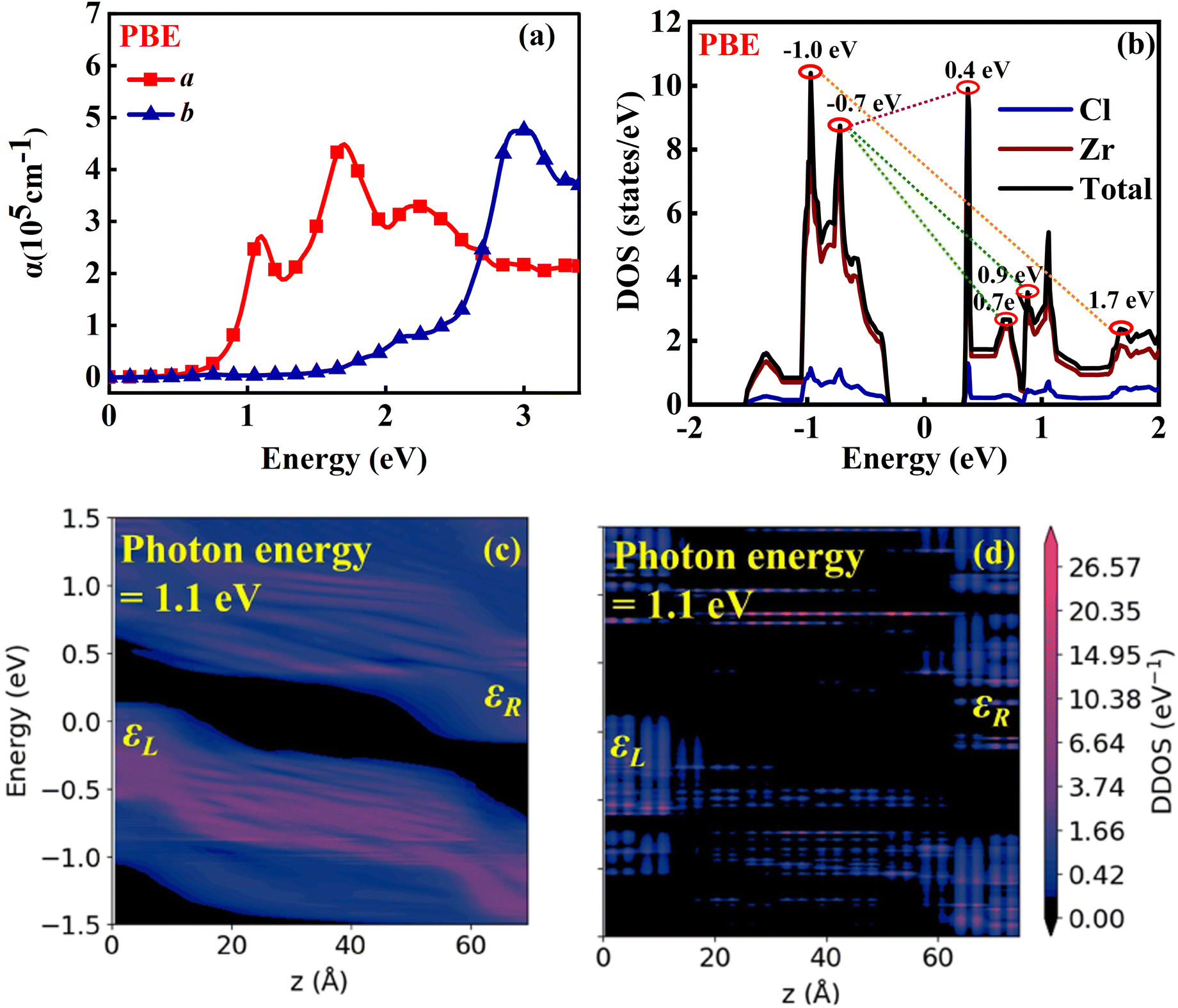
The monolayer O1 variant of 1T′ phase ZrCl2, with a space group of P21/m, was obtained from the corresponding bulk (space group no. 31, Pmn21). We confirmed the phonon spectrum and molecular dynamics stability of the O1 variant (see Fig. S1, ESI†), in line with prior research.36,59 Previous theoretical studies also supported its formation energy and mechanical stability.36,59 The optimized cell, as shown in Fig. 1, exhibits lattice parameters of a = 3.33 Å and b = 6.23 Å, containing two Zr atoms and four Cl atoms. The bond lengths formed by Zr-1 and Cl-1 (2) atoms are 2.62 Å, and by Zr-2 and Cl-3 (4) atoms are 2.66 Å and 2.73 Å, respectively. These values are consistent with previous theoretical calculations.36,59 The bond angles formed by Cl-2 and Zr-1 (2) atoms is 70.09°, and by Zr-2 and Cl-3 (4) atoms is 81.43°. These values closely match those obtained from the MatHub-2d database, which are 70.37° and 81.29°, respectively.60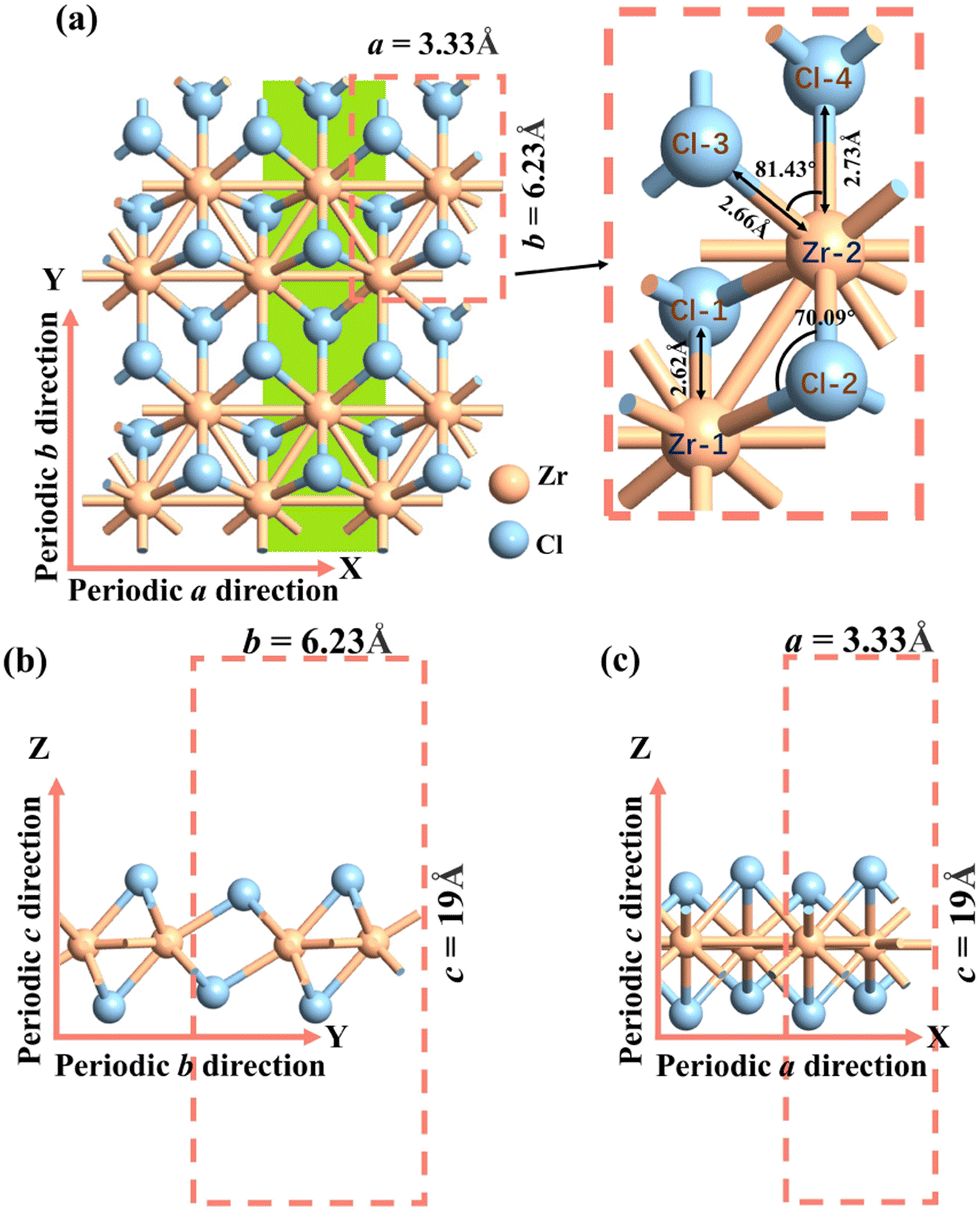 | ||
| Fig. 1 Atomic structure of (a) top view, (b) and (c) side view of the O1 variants. a and b are the lattice constants of the 2D plane, and c is the lattice constant in the vacuum layer direction. In order to better illustrate how the O2 and O3 variants are obtained by rotating the O1 variant by 120° (Section 3.2.3, Fig. 5), we have highlighted the armchair Zr–Cl chain in green. | ||
Monolayer O1 variant of ZrCl2 exhibits a quasi-direct bandgap of 0.60/1.15 eV (PBE/HSE06) with a tiny difference between the direct and indirect bandgaps (Edirect − Eindirect = 6 meV), where both the VBM and the CBM lie between the Γ and X points as shown in Fig. 2(a) and (b). These computational results agree with previous research data.36,59–61Fig. 2(c) illustrates the impact of spin–orbit coupling (SOC) on the band structure, revealing a minimal bandgap adjustment of 0.001 eV, while the general band structure remains largely unchanged. Hence, SOC effects are not considered in our subsequent research.62
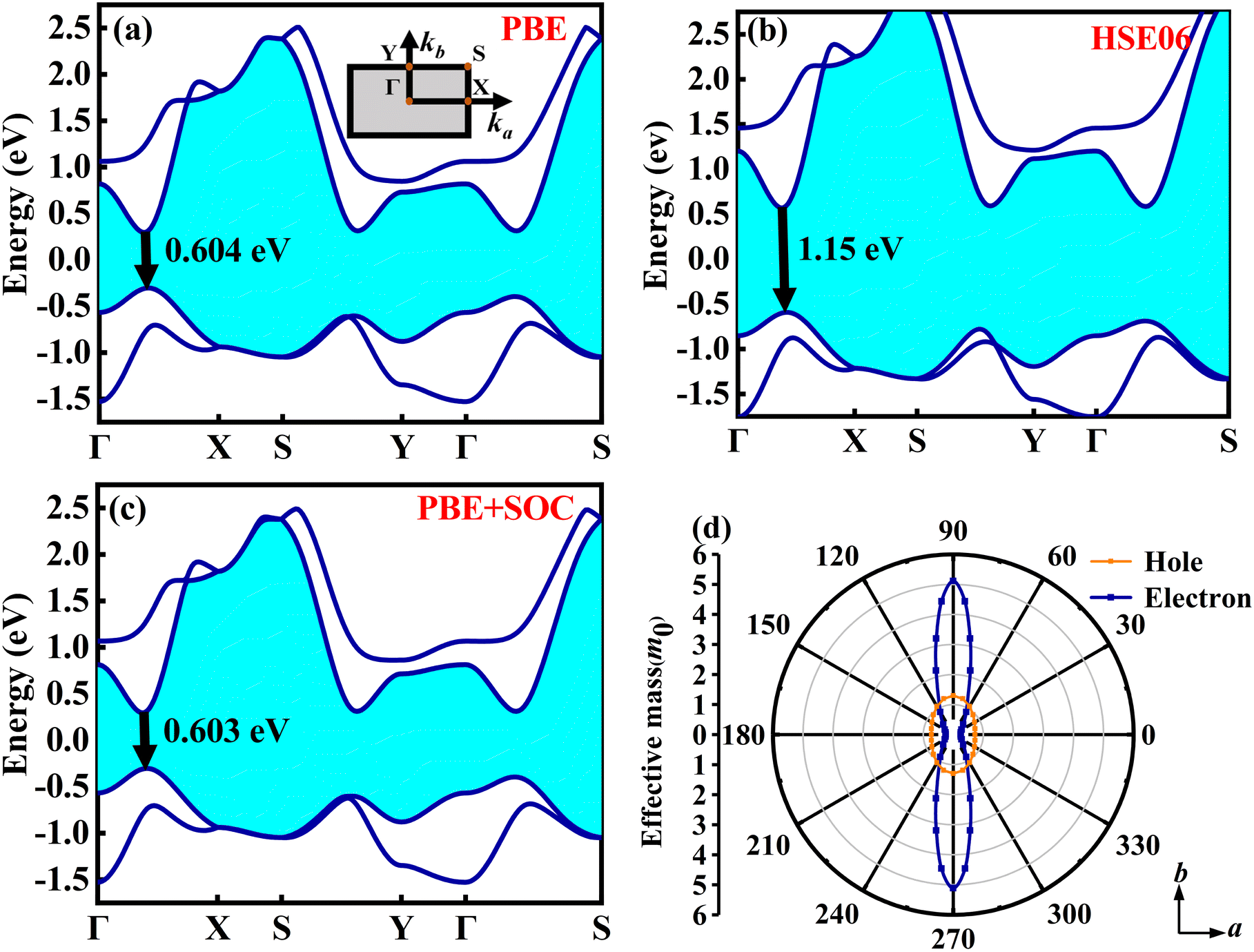 | ||
| Fig. 2 The band structure of the O1 variant was calculated using the (a) PBE functional and (b) HSE06 functional, (c) PBE method considering the SOC effect, and (d) angular dependence of effective mass m* for holes and electrons. The inset in (a) shows the Brillouin zone. | ||
3.2 Electronic transport properties
 in the b direction is approximately twenty times higher than in the a direction, indicating a strong directional dependence. Conversely, for holes, the effective mass
  in the b direction is only 1.7 times higher than in the a direction. Comparing carrier types, in the a direction,
  is three times that of electrons, while in the b direction, this relationship inverts, with
  being about four times that of holes. The effective mass of electrons in the a direction is smaller compared to several other 2D materials, such as MoS2 (0.47 m0),63 MoSe2 (0.55 m0),63 As2S3 (1.70 m0),64 Zn2VN3 (2.15 m0),65 WS2 (0.31 m0),63 WSe2 (0.34 m0),63 VP (1.44 m0),66 GeAs2 (0.27 m0),67 SiAs2 (0.42 m0).68
| Carrier | m* (m0) | E l (eV) | C 2D (N m−1) | µ (cm2 V−1 s−1) |
|---|---|---|---|---|
| e(a) | 0.247 | −0.262 | 82.83 | 1.44 × 10⁴ |
| e(b) | 5.112 | 1.622 | 66.76 | 0.26 × 10³ |
| h(a) | 0.726 | 3.014 | 82.83 | 0.48 × 10³ |
| h(b) | 1.299 | 0.646 | 66.76 | 0.46 × 10³ |
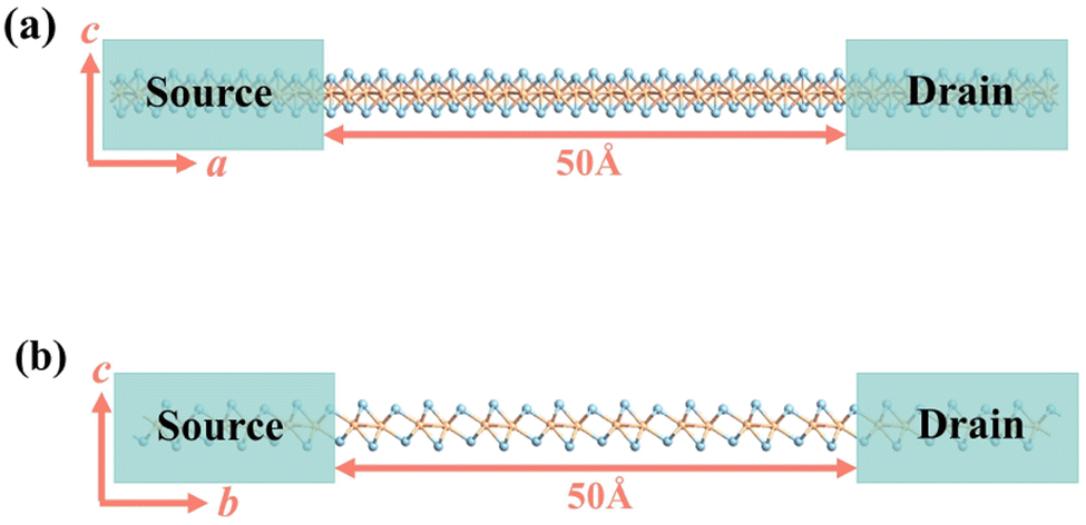 | ||
| Fig. 3 Schematic diagrams of the two-probe system for computing the electric transport of monolayer O1 variant of ZrCl2 in (a) the a direction and (b) the b direction. The channel length is 50 Å. | ||
Fig. 4(a) displays the I–V curves in the a and b directions, indicating a noticeable anisotropy. The current in the a direction rises as the bias voltage increases, resulting in a conductive state; conversely, the current in the b direction remains in the off state. The maximum current on/off ratio occurs at −0.4 V, reaching 106, which is comparable to or even better than those reported for other 2D materials or molecular devices, such as GeC2 (105),76 GaPS (105),77 borophosphene (105),78 cyclo[18]carbon (104).79
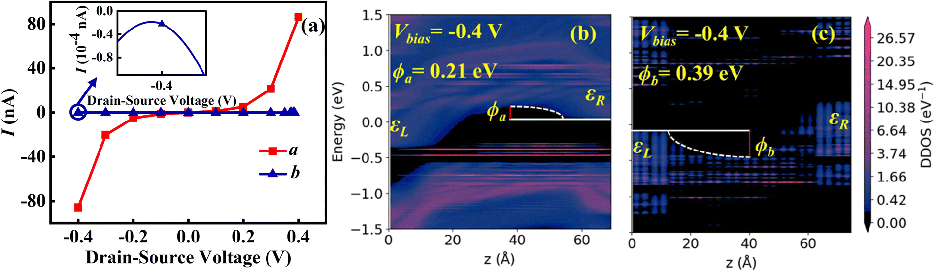 | ||
| Fig. 4 (a) The I–V characteristic curves of the O1 variants in the a direction and b direction, the inset is an enlarged view along the b direction at −0.4 V bias voltage. (b) Along the a direction and (c) b direction, the device of the density of states (DDOS) for the two-probe configuration of the O1 variant under −0.4 V bias. | ||
To further explain the phenomenon of the maximum current on/off ratio observed at a bias of −0.4 V, we calculated the DDOS along the a and b directions under this bias. As shown in Fig. 4(b) and (c), the effective barrier height in the a direction ϕa is 0.21 eV, while in the b direction ϕb is 0.39 eV. This significant difference in barrier height directly influences carrier transport properties. The lower barrier in the a direction means that carriers more easily overcome the barrier in the a direction, leading to an “on” state in the a direction and an “off” state in the b direction. Further analysis of the DDOS distribution shows that the a direction exhibits a higher and more uniformly distributed density of states, which facilitates continuous electron transport and likely results in higher conductivity. In contrast, the uneven DDOS distribution in the b direction may increase carrier scattering, thereby reducing conductivity. These mechanisms account for the observed current maximum on/off ratio.
The monolayer 1T′ phase of ZrCl2 under investigation is both its ground state and ferroelastic phase.36 The formation of a ferroelastic phase typically arises from a reduction in the symmetry of the prototype structure, leading to a structural phase transition. This low-symmetry ferroelastic phase is characterized by multiple orientation states, manifesting as different spontaneous strains relative to the unit cell of the prototype phase. Specifically, the 1T′ phase of monolayer ZrCl2 exhibits three energy-degenerate but structurally inequivalent variants O1, O2, and O3. These variants emerge from a Peierls distortion induced by the Fermi surface nesting in the prototype 1T structure, resulting in distorted octahedral coordination. This distortion causes spontaneous dimerization of Zr atoms along high-symmetry [100], [010], or [110] directions, thereby enabling a 2D three-state ferroelasticity. Fig. 5 depicts the O1, O2, and O3 variants of monolayer 1T′ phase ZrCl2. The O1 variant displays intrinsic ferroelasticity, featuring an unusual 120° rotational transformation. It can convert to the O2 or O3 variants by overcoming a moderate energy barrier of 24–39 meV per atom. Notably, the O2 and O3 variants display mirror symmetry with respect to the Y-axis, highlighting the structural relationships among these ferroelastic states.28,36 Given this symmetry and considering our device configuration, O2 and O3 are expected to produce equal but oppositely directed electric current (photocurrent). By analyzing O3 in detail, we not only gain direct insights into its behavior but can also infer the corresponding characteristics of O2 through simple directional inversion, enabling a comprehensive understanding of the entire system.
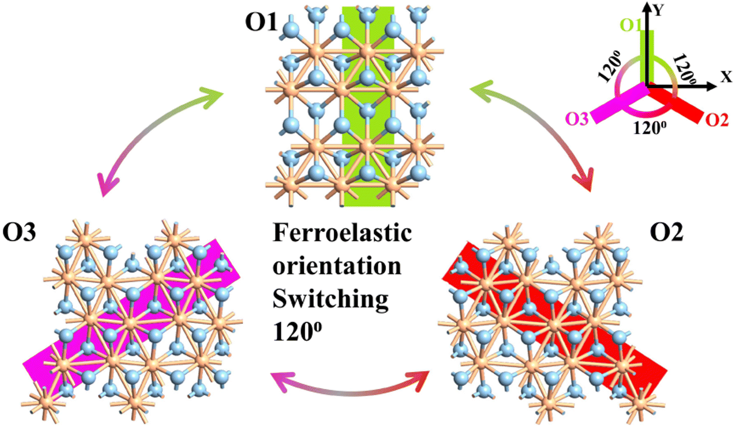 | ||
| Fig. 5 The top views of the O1, O2, and O3 variants, respectively. The green, red, and purple highlighted portions represent the Zr–Cl chains of the O1, O2, and O3 variants. The illustration in the top right provides a simplified diagram of the 120° rotational relationship between the O1, O2, and O3 variants, as well as the Y-axis mirror symmetry between O2 and O3. | ||
We further calculated the electron and hole transport properties of the O3 variant along the a and b directions. As shown in Fig. 6(a), in the voltage range of −0.4 V to 0.4 V, both directions exhibit high current values, peaking at approximately 500–600 nA, far exceeding the range observed in the O1 variant (80 nA). This indicates that the O3 variant demonstrates excellent conductivity for both electron and hole transport, with no distinct switching behavior. To better understand this phenomenon, we calculated the DDOS in both directions under −0.4 V bias, as shown in Fig. 6(b) and (c). The analysis reveals that the effective barrier height in the a direction ϕa is 0.05 eV, and in the b direction ϕb is 0.06 eV. The barrier heights are similar in both directions and significantly lower than those in the O1 variant, facilitating efficient carrier injection and transport. From the perspective of structural symmetry, the one-dimensional arrangement of Zr–Cl chains in the O1 variant leads to pronounced structural differences between the chain direction and the direction perpendicular to the chains, resulting in strong anisotropy in electrical transport. The O3 variant, with its 120° rotated Zr–Cl chains, forms a more uniform structure. In this configuration, Zr atoms are arranged into a hexagonal network, with Cl atoms symmetrically distributed around them. This structural homogeneity reduces directional anisotropy, yielding similar electron and hole transport properties along the a and b directions, respectively.
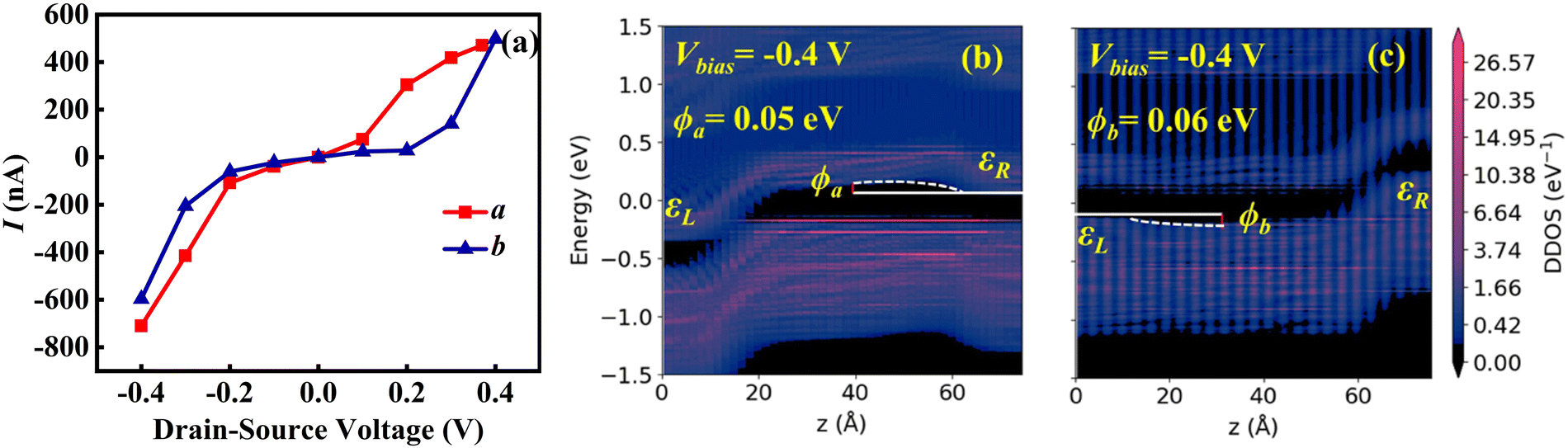 | ||
| Fig. 6 (a) The I–V characteristic curves of the O3 variant along the a and b directions. (b) Along the a direction and (c) b direction, DDOS for the two-probe configuration of the O3 variant under −0.4 V bias. | ||
The distinct electronic transport characteristics of the O1 and O3 variants open up exciting possibilities for designing versatile and high-performance nanoelectronic devices.37,42 The O1 variant, with its high current on/off ratio (106) and strong anisotropic conductivity, shows great potential for high-performance FETs, logic gates, and memory devices where precise current control and switching capabilities are crucial. Its anisotropic nature could also be exploited in the development of direction-sensitive sensors or in creating novel electronic circuits with directional conductivity. On the other hand, the O3 variant's high and nearly isotropic conductivity in both directions makes it an excellent candidate for applications requiring uniform current flow, such as transparent electrodes, interconnects in integrated circuits, or as channels in high-performance bipolar transistors. Its lack of distinct switching behavior could be advantageous in applications where consistent conductivity is needed across varying electric fields.
3.3 Photocurrent transport properties
To comprehensively understand the material's capabilities, we extended our investigation with a particular focus on the photocurrent characteristics of the monolayer O1 variant of ZrCl2 in a practical device context. For this purpose, we designed and constructed a two-probe model of a ZrCl2 photovoltaic p–i–n junction, as illustrated in Fig. 7. This structure consists of a p-doped region, an intrinsic (i) region, and an n-doped region. The central i region has a length of 50 Å. Both p and n regions have doping concentrations of 1014 cm−2. At the heart of this device, the i region serves as the primary area for polarized light absorption, effectively capturing incident photons. The built-in electric field between the p and n regions spans the entire i region, promoting the separation of photogenerated electron–hole pairs. Subsequently, these separated electrons and holes move towards the n and p regions, respectively, generating a measurable photocurrent. This design utilizes the photovoltaic effect to achieve high-performance self-powered photodetection, providing an ideal platform for studying the complete physical process from photon absorption to charge separation and transport in ZrCl2.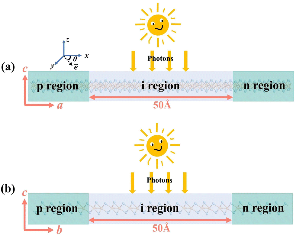 | ||
Fig. 7 The p–i–n junction diagram of the monolayer O1 variant of ZrCl2 in (a) the a direction and (b) the b direction, θ is the polarization angle of linearly polarized light. ![[e with combining right harpoon above (vector)]](https://www.rsc.org/images/entities/i_char_0065_20d1.gif) is the polarization vector of linearly polarized light. is the polarization vector of linearly polarized light. | ||
The presence of heavily doped regions in our p–i–n structure significantly influences the choice of computational method for photocurrent calculations. While the GW method is known for its accuracy in predicting band gaps, it becomes less suitable for heavily doped 2D semiconductors as the GW band gap narrows due to enhanced screening of many-body effects. In such scenarios, DFT based on single-electron approximation, particularly the PBE functional, becomes more appropriate. Although PBE generally underestimates band gaps, heavy doping brings the effective band gap closer to PBE predicted values, making it a computationally efficient choice without significant loss of accuracy.80,81 This approach is supported by previous studies, which have shown that GGA methods yield photocurrent results for 2D materials like MoS2, WSe2, and BP that are in high agreement with experimental data.82–85 Considering these factors, we employed the PBE method for our photocurrent calculations, expecting it to provide reliable results for our heavily doped ZrCl2 p–i–n structure while avoiding the computational intensity and potential inaccuracies of GW methods in this specific context (details in the ESI†).
Photocurrent density Jph is a key performance metric in optoelectronic devices, representing the photocurrent generated per unit area under illumination. It directly reflects a material's light absorption and photoelectric conversion capabilities. To comprehensively evaluate device efficiency, photo responsivity Rph and external quantum efficiency EQE are also crucial. These metrics are defined as:86
 | (7) |
R ph (measured in A W−1) quantifies the current output relative to incident light power, directly indicating the device's light-to-current conversion efficiency. EQE, a dimensionless ratio of generated electrons to incident photons, provides insight into the quantum efficiency of photoelectric conversion across different wavelengths. While Rph offers a straightforward measure of device sensitivity, EQE accounts for photon energy, making it valuable for spectral performance analysis. Together, these metrics provide a comprehensive assessment of optoelectronic device performance.
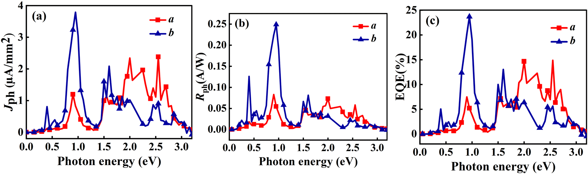
Initially, we analyzed the Jph generated under incident light with an in-plane θ of 0°. As depicted in Fig. 8(a), the O1 variant exhibits pronounced anisotropy in the Jph along the a and b directions. In the a direction, the Jph reaches two distinct peaks: 6.57 µA mm−2 at a photon energy of 1.1 eV and 5.90 µA mm−2 in the 1.5–1.6 eV range, which is even better than that of other 2D materials. For example NaCuTe (1.68 µA mm−2),87 NaCuSe (0.65 µA mm−2),87 NaCuS (0.66 µA mm−2),87 and InSe (0.018 µA mm−2).88 Additionally, a noticeable upward trend in Jph is observed in the energy range of 2.8–3.0 eV. In contrast, the Jph along the b direction is generally lower, with only a minor peak of 0.39 µA mm−2 at a photon energy of 2.7 eV. Notably, these peaks coincide with the absorption peak of the material (Fig. 9(a)).
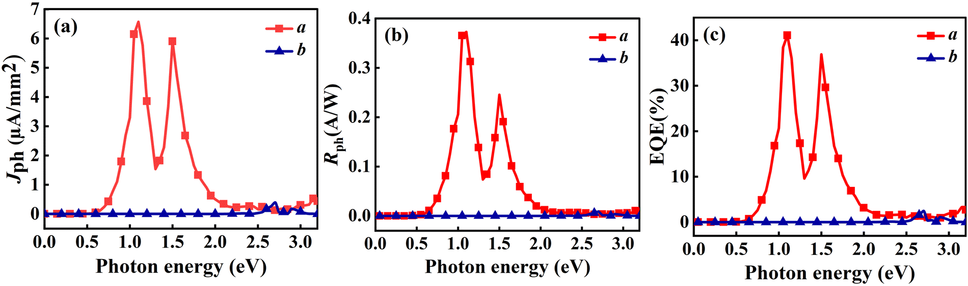 | ||
| Fig. 8 Linearly polarized light with θ of 0° incident on the O1 variant, showing (a) Jph, (b) Rph, and (c) EQE as functions of photon energy. | ||
 | ||
| Fig. 9 (a) The optical absorption coefficient and (b) density of states (DOS) of the O1 variant calculated using the PBE methods. (c) Along the a direction and (d) b direction, DDOS for the two-probe configuration of the O1 variant under photon energy 1.1 eV. | ||
To further understand the origin of the Jph peaks, we calculated and analyzed the DOS for the O1 variant. According to Fermi's golden rule, the probability of electron transitions from the valence band to the conduction band is proportional to the DOS. Therefore, electron transitions between energy levels at DOS peaks are more likely, resulting in stronger photocurrent. By comparing the DOS (Fig. 9(b)) with the Jph spectrum, we can elucidate the key photocurrent features along the a direction. The primary photocurrent peak around 1.1 eV is attributed to electron transitions from near the valence band (approximately −0.7 eV) to the CBM (around 0.4 eV), corresponding to the high DOS at these energy levels. The secondary peak around 1.5 eV likely results from transitions between states near the VBM (around −0.7 eV) and those slightly above the CBM (0.7–0.9 eV), aligning with the DOS distribution that shows an energy difference of approximately 1.4–1.6 eV. The photocurrent rise observed around 3.0 eV may correspond to electron transitions from the deeper valence band (around −1.0 eV) to higher energy states in the conduction band (around 2.0 eV). Although the DOS around 2.0 eV is relatively low, the energy alignment still facilitates a measurable photocurrent.
The pronounced anisotropy in Jph can be explained by the band structure, partial charge density, and DDOS. As shown in Fig. 2(a), both the CBM and VBM are located along the Γ–X path, i.e., in the a direction. This band structure significantly enhances the probability of photon-induced electron–hole pair separation along the a direction compared to the b direction. The partial charge density analysis further confirms that electrons are primarily distributed along the a direction (see Fig. S4, ESI†). This allows the excited electrons to more easily transport in this direction, resulting in a much higher Jph along the a direction than the b direction. Notably, under 1.1 eV photon illumination, the Jph along the a direction is 106 times greater than that along the b direction. Fig. 9(c) and (d) depicts the DDOS for the a and b directions under 1.1 eV photon energy, revealing a higher and more continuously distributed electron density along the a direction compared to the b direction, which elucidates the observed anisotropy in Jph.
Fig. 8(b) and (c) illustrate the variation of Rph and EQE with photon energy for the O1 variant along the a and b directions. Along the a direction, Rph reaches peaks of 0.37 A W−1 at 1.1 eV and 0.25 A W−1 at 1.5 eV, respectively, significantly surpassing the maximum value of 0.009 A W−1 observed in the b direction. Notably, the Rph of ZrCl2 along the a direction outperforms several reported 2D materials, including MoS2 (0.016 A W−1),89 InS (0.13 A W−1),88 InSe (0.18 A W−1),88 NaCuTe (0.105 A W−1),87 and graphene (10−4 A W−1).84 In line with the responsivity, EQE peaks at 41.08% and 36.85% at 1.1 eV and 1.5 eV, respectively, along the a direction. In contrast, EQE in the b direction remains low across most of the energy spectrum, with a maximum of only 2.46%. This pronounced anisotropy further confirms the unique optoelectronic properties of the O1 variant. Moreover, the EQE along the a direction exceeds that of various 2D materials, such as SnS (22.01%),90 NaCuTe (34.3%),87 NaCuSe (8%),87 and KagSe (17.9%).89 In the higher energy range of 2.8–3.0 eV, although the increase in responsivity is less prominent, the EQE exhibits a noticeable rise, forming a small peak. In summary, the combination of high performance and anisotropic response also opens up possibilities for novel optoelectronic logic gates or optical switches based on polarization control. Additionally, the superior EQE compared to many other 2D materials indicates potential for high-efficiency photovoltaic devices, particularly in tandem solar cell architectures where specific wavelength ranges need to be targeted.
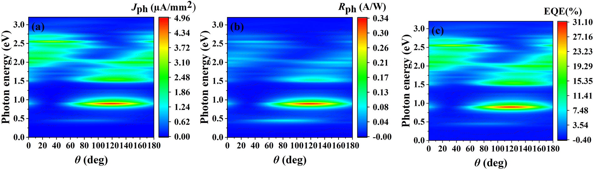
To gain a more comprehensive understanding of the optoelectronic properties of the O1 variant, we further investigated the relationship between Jph, Rph, and EQE with respect to the θ and photon energy, as shown in Fig. 10. All three parameters exhibit a strong dependence on both photon energy and θ, following a highly consistent pattern. The most prominent feature is the appearance of three distinct response peaks: a primary peak around 1.1 eV, a secondary peak near 1.5 eV, and a weaker but noticeable high-energy peak at approximately 2.8 eV. Notably, the variation of Jph with θ in the ZrCl2 photodetector follows the relation: Jph(E) = A(E) + B(E)[sin(2θ + ϕ(E))],91–94 where A, B and ϕ are coefficients related to energy and structure. Additionally, we observed that the angular dependence of Rph and EQE follows a similar trend to that of Jph.
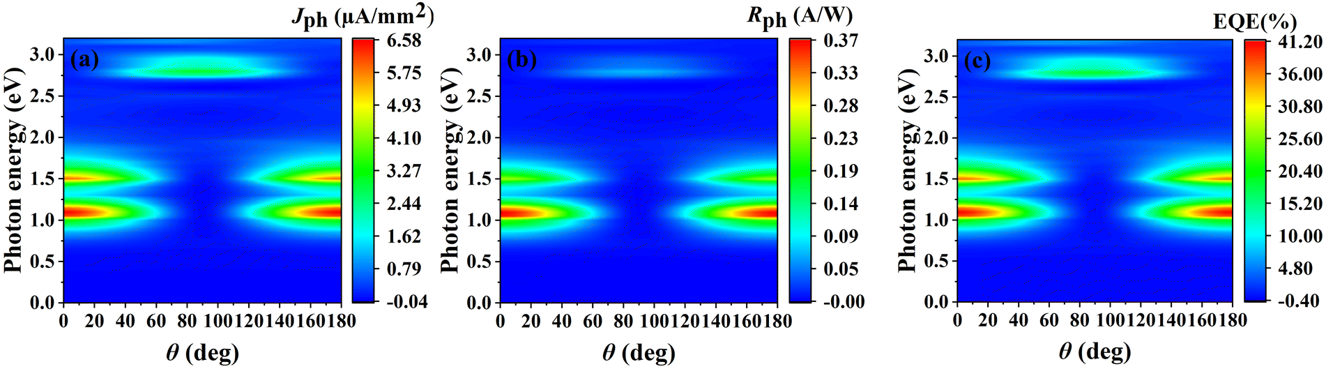 | ||
| Fig. 10 (a) Jph, (b) Rph, and (c) EQE of the O1 variant with respect to photon energy and θ for linearly polarized light incident along the a direction. | ||
To further elucidate this behavior, we focused on three representative photon energies: 1.1 eV, 1.5 eV, and 2.8 eV (detailed angular dependence data are provided in Fig. S5, ESI†). The angular response shows distinct patterns at different photon energies. At 1.1 eV and 1.5 eV, a cosine-like distribution is observed, with maxima at θ ≈ 0° and 180°, and minima at θ ≈ 90°. In contrast, at 2.8 eV, an opposite sine-like behavior emerges, with peaks at θ ≈ 90° and minima at θ ≈ 0° and 180°. This angular dependence maintains symmetrical distribution over the 0° to 180° range across the entire measured energy spectrum, although the response intensity varies with photon energy. This unique omnidirectional photoresponse not only confirms the strong anisotropy of the O1 variant but also suggests potential applications in various advanced fields.95 The device exhibits clear spectral selectivity, with primary high-sensitivity response in the near-infrared region (1.1 eV and 1.5 eV, corresponding to approximately 1129 nm and 828 nm), making it well-suited for near-infrared imaging, spectroscopy, and telecommunications. Additionally, a discernible response in the visible blue-violet spectrum (2.8 eV, ∼443 nm) extends the device's functionality to the visible light range. This multi-band detection capability, combined with strong angular dependence, enables effective operation across diverse optical environments spanning from near-infrared to visible light spectra, particularly for polarization-sensitive applications.
Fig. 11 illustrates Jph, Rph, and EQE characteristics of the O3 variant along the a and b directions under an in-plane θ of 0°. Both directions show significant responses, with notable features in both low and high-energy ranges. For the a direction (red curves), multiple prominent peaks are observed in the high-energy range (1.5–3.0 eV), which are generally larger than the peak in the low-energy range (approximately 0.8–1.0 eV), particularly for Jph and EQE. In the Rph plot, these peaks are comparable in magnitude. The b direction (blue curves) shows a stronger peak in the low-energy range but generally weaker response in the high-energy range compared to the a direction. Detailed analysis reveals that the Jph along the b direction reaches its main peak (∼4 µA mm−2) at 0.95 eV, while the a direction displays several peaks in the high-energy region (∼2 µA mm−2). Similarly, Rph follows a comparable trend, with a main peak of approximately 0.25 A W−1 in the b direction. The EQE reaches a peak of about 23% at 0.95 eV in the b direction, while the highest EQE in the high-energy range along the a direction is around 15%. In contrast, the O1 variant demonstrates strong anisotropy, with significant response primarily along the a direction. Two distinct peaks appear at around 1.0 eV and 1.5 eV, with higher magnitudes (Jph ∼ 6.57 µA mm−2, Rph ∼ 0.37 A W−1 and EQE reaching up to 41.08%), while the b direction shows almost no response. This pronounced difference in structure-related optoelectronic properties opens new possibilities for developing innovative mechanical sensors. By accurately measuring changes in the optoelectronic response, it is possible to detect whether the material has undergone a phase transition from O1 to O3, enabling the detection of shear stress on the material surface. Most importantly, this type of sensor can be self-powered using sunlight, eliminating the need for an external power source, which offers a significant advantage for remote or hard-to-access environmental monitoring applications.
 | ||
| Fig. 11 Linearly polarized light with θ of 0° generates (a) Jph, (b) Rph, and (c) EQE in the O3 variant when incident in the a and b directions. | ||
Furthermore, we investigated the relationships between the Jph, Rph, and EQE with θ and photon energy in both the a and b directions, as shown in Fig. 12 (additional angular dependence data for the b direction are provided in Fig. S6, ESI†). The distributions of Jph, Rph, and EQE exhibit similar patterns overall. All three quantities reach their maximum values in the low-energy region (approximately 0.8–1.0 eV). For the a direction, the maxima appear at θ between 110° and 130°, with Jph reaching 4.96 µA mm−2, Rph at 0.34 A W−1, and EQE at 31%. Similar behavior is observed in the b direction, where the maximum values occur within the range of 140°–160°, with comparable magnitudes (Jph: 4.93 µA mm−2, Rph: 0.32 A W−1, and EQE: 31%, see Fig. S6, ESI†).
 | ||
| Fig. 12 (a) Jph, (b) Rph, and (c) EQE of the O3 variant with respect to photon energy and θ for the linearly polarized light incident along the a direction. | ||
Significant differences were observed in the angular and spectral dependencies of Jph, Rph, and EQE between the O1 and O3 variants. The O1 variant exhibits a characteristic symmetric pattern, with the response highly concentrated near 0° and 180° (a direction), and higher maximum values (Jph 6.57 µA mm−2, Rph 0.37 A W−1, EQE 41.08%), along with two distinct response bands at approximately 1.0 eV and 1.5 eV. In contrast, the angular and spectral dependencies of Jph, Rph, and EQE for the O3 variant show less symmetry, with the response distributed over a broader range of angles and photon energies. The O3 variant also demonstrates lower maximum values (Jph 4.96 µA mm−2, Rph 0.34 A W−1, EQE 31%) compared to the O1 variant, but exhibits a more balanced response across different angles and a wider spectral range. These differences reflect the distinct dimerization directions of Zr atoms in the two variants. The dimerization in the [100] direction of the O1 variant leads to strong anisotropy and specific energy responses, making it more suitable for applications requiring highly directional selectivity. Conversely, the [110] dimerization in the O3 variant results in a more balanced response, providing potential advantages in applications requiring wide spectral and multi-directional photodetection, such as omnidirectional sensors or broadband photodetectors. This distinction between the two variants opens up possibilities for designing tunable multifunctional optoelectronic devices. By switching between the O3 and O1 variants, it is possible to achieve dynamic transitions between omnidirectional response and high-sensitivity directional response, adapting to varying operational environments and requirements.
4 Conclusions
Our comprehensive study of monolayer 1T′ phase ZrCl2 reveals striking differences between its O1 and O3 ferroelastic variants, demonstrating the profound impact of structural transitions on material properties. The O1 variant exhibits exceptional anisotropy, with ultra-high electron mobility (1.44 × 104 cm2 V−1 s−1) and current on/off ratio (106) along the a direction, alongside strong photoresponse anisotropy (Jph: 6.57 µA mm−2, Rph: 0.37 A W−1, EQE: 41.08%). In contrast, the O3 variant shows more isotropic behavior, with high conductivity in both directions (500–600 nA at ±0.4 V) and a balanced photoresponse (Jph: 4.96 µA mm−2, Rph: 0.34 A W−1, EQE: 31%) across a broader spectrum. The ability to switch between these variants through ferroelastic transitions offers unprecedented opportunities for creating adaptive electronic and optoelectronic devices. By controlling Zr–Cl chain dimerization, we can potentially achieve dynamic regulation of material properties, leading to reconfigurable circuits, multi-state memory devices, and tunable sensors. Furthermore, the coexistence of variants with distinct properties opens possibilities for novel heterostructures and domain wall devices. This research not only deepens our understanding of 2D ferroelastic materials but also paves the way for new concepts in nanoelectronics and optoelectronics, positioning monolayer 1T′ ZrCl2 as a promising platform for next-generation technologies in information processing, energy conversion, and sensing.Data availability
The data that support the findings of this study are available from the corresponding author upon reasonable request.Conflicts of interest
The authors declare that they have no conflict of interest.Acknowledgements
Calculations were carried out in the High-Performance Computing Laboratory of Changzhou University and Hefei Advanced Computing Center. The authors extend their gratitude to the Stork's Writing Assistant (https://www.storkapp.me/writeassistant/) for its assistance in polishing some of the text in this article.References
- S. Joseph, J. Mohan, S. Lakshmy, S. Thomas, B. Chakraborty, S. Thomas and N. Kalarikkal, Mater. Chem. Phys., 2023, 297, 127332 CrossRef CAS.
- S. Chowdhury and D. Jana, Rep. Prog. Phys., 2016, 79, 126501 CrossRef.
- X. Tang, Q. Hao, X. Hou, L. Lan, M. Li, L. Yao, X. Zhao, Z. Ni, X. Fan and T. Qiu, Adv. Mater., 2024, 36, 2312348 CrossRef CAS PubMed.
- P. Kumbhakar, C. Chowde Gowda and C. S. Tiwary, Front. Mater., 2021, 8, 721514 CrossRef.
- J. Hu and M. Dong, J. Nanobiotechnol., 2024, 22, 63 CrossRef PubMed.
- Y. Wu, W. Yuan, M. Xu, S. Bai, Y. Chen, Z. Tang, C. Wang, Y. Yang, X. Zhang, Y. Yuan, M. Chen, X. Zhang, B. Liu and L. Jiang, Chem. Eng. J., 2021, 412, 128744 CrossRef CAS.
- A. VahidMohammadi, M. Mojtabavi, N. M. Caffrey, M. Wanunu and M. Beidaghi, Adv. Mater., 2019, 31, 1806931 CrossRef.
- S. Manzeli, D. Ovchinnikov, D. Pasquier, O. V. Yazyev and A. Kis, Nat. Rev. Mater., 2017, 2, 17033 CrossRef CAS.
- W. Zhang, Z. Huang, W. Zhang and Y. Li, Nano Res., 2014, 7, 1731–1737 CrossRef CAS.
- C. Li, D. Sang, S. Ge, L. Zou and Q. Wang, Molecules, 2024, 29, 3341 CrossRef CAS.
- X. Yin, C. S. Tang, Y. Zheng, J. Gao, J. Wu, H. Zhang, M. Chhowalla, W. Chen and A. T. S. Wee, Chem. Soc. Rev., 2021, 50, 10087–10115 RSC.
- A. Ahmed, M. Zahir Iqbal, A. Dahshan, S. Aftab, H. H. Hegazy and E. S. Yousef, Nanoscale, 2024, 16, 2097–2120 RSC.
- G.-B. Liu, D. Xiao, Y. Yao, X. Xu and W. Yao, Chem. Soc. Rev., 2015, 44, 2643–2663 RSC.
- M. A. Khan and M. N. Leuenberger, Nanophotonics, 2018, 7, 1589–1600 CrossRef CAS.
- J. Zhang, L. Du, S. Feng, R.-W. Zhang, B. Cao, C. Zou, Y. Chen, M. Liao, B. Zhang, S. A. Yang, G. Zhang and T. Yu, Nat. Commun., 2019, 10, 4226 CrossRef.
- M. Zhang, Y. Zhu, X. Wang, Q. Feng, S. Qiao, W. Wen, Y. Chen, M. Cui, J. Zhang, C. Cai and L. Xie, J. Am. Chem. Soc., 2015, 137, 7051–7054 CrossRef CAS.
- H. Zhang, F. Guégan, J. Wang and G. Frapper, Phys. Chem. Chem. Phys., 2024, 26, 14675–14683 RSC.
- X. Huang, L. Yan, Y. Zhou, Y. Wang, H.-Z. Song and L. Zhou, J. Phys. Chem. Lett., 2021, 12, 525–531 CrossRef CAS PubMed.
- H. Han, M. Hong, S. S. Gokhale, S. B. Sinnott, K. Jordan, J. E. Baciak and J. C. Nino, J. Phys. Chem. C, 2014, 118, 3244–3250 CrossRef CAS.
- Y. Zhang, S. Li, W. Yang, M. K. Joshi and X. Fang, J. Phys. Chem. Lett., 2019, 10, 2400–2407 CrossRef CAS.
- A. Aji Suleiman, X. Zhou and T. Zhai, J. Phys. D: Appl. Phys., 2021, 54, 013002 CrossRef.
- D. Torelli, H. Moustafa, K. W. Jacobsen and T. Olsen, npj Comput. Mater., 2020, 6, 158 CrossRef.
- D. C. Hvazdouski, M. S. Baranava, E. A. Korznikova, A. A. Kistanov and V. R. Stempitsky, 2D Mater., 2024, 11, 025022 CrossRef CAS.
- L. Wang, T. Lin, J. Wang, C. Fang, Y. Li and Y. Qiao, Phys. Chem. Chem. Phys., 2024, 26, 26857–26870 RSC.
- J. Kim, K.-W. Kim, B. Kim, C.-J. Kang, D. Shin, S.-H. Lee, B.-C. Min and N. Park, Nano Lett., 2020, 20, 929–935 CrossRef CAS.
- P. Man, L. Huang, J. Zhao and T. H. Ly, Chem. Rev., 2023, 123, 10990–11046 CrossRef CAS.
- H. Wang, Y. Wen, H. Zeng, Z. Xiong, Y. Tu, H. Zhu, R. Cheng, L. Yin, J. Jiang, B. Zhai, C. Liu, C. Shan and J. He, Adv. Mater., 2024, 2305044 CrossRef PubMed.
- W. Li and J. Li, Nat. Commun., 2016, 7, 10843 CrossRef CAS PubMed.
- H. Wang and X. Qian, 2D Mater., 2017, 4, 015042 CrossRef.
- Y. Yang, H. Zong, X. Ding and J. Sun, Appl. Phys. Lett., 2022, 121, 122903 CrossRef CAS.
- Z. Tu and M. Wu, Sci. Bull., 2020, 65, 147–152 CrossRef CAS.
- X. Xu, Y. Ma, T. Zhang, C. Lei, B. Huang and Y. Dai, Nanoscale Horiz., 2020, 5, 1386–1393 RSC.
- L. Yang, Y. Gao, M. Wu and P. Jena, Phys. Rev. B, 2022, 105, 094101 CrossRef CAS.
- C. Xu, J. Mao, X. Guo, S. Yan, Y. Chen, T. W. Lo, C. Chen, D. Lei, X. Luo, J. Hao, C. Zheng and Y. Zhu, Nat. Commun., 2021, 12, 3665 CrossRef CAS.
- X. Xiao, J. Zhou, K. Song, J. Zhao, Y. Zhou, P. N. Rudd, Y. Han, J. Li and J. Huang, Nat. Commun., 2021, 12, 1332 CrossRef CAS.
- X. Huang, Z. Zhuo, L. Yan, Y. Wang, N. Xu, H.-Z. Song and L. Zhou, J. Phys. Chem. Lett., 2021, 12, 7726–7732 CrossRef CAS.
- X. Lu, Z. Chen, Y. Cao, Y. Tang, R. Xu, S. Saremi, Z. Zhang, L. You, Y. Dong, S. Das, H. Zhang, L. Zheng, H. Wu, W. Lv, G. Xie, X. Liu, J. Li, L. Chen, L.-Q. Chen, W. Cao and L. W. Martin, Nat. Commun., 2019, 10, 3951 CrossRef PubMed.
- W. Lei, R. Hu, S. Han, H. Yuan, W. Jiao, Y. Luo and H. Liu, J. Phys. Chem. C, 2024, 128, 543–548 CrossRef CAS.
- Y. Shen and Q. Wang, Phys. Rep., 2022, 964, 1–42 CrossRef CAS.
- M. Wu and X. C. Zeng, Nano Lett., 2016, 16, 3236–3241 CrossRef CAS PubMed.
- S. Zhu, R. Duan, X. Xu, F. Sun, W. Chen, F. Wang, S. Li, M. Ye, X. Zhou, J. Cheng, Y. Wu, H. Liang, J. Kono, X. Li, Z. Liu and Q. J. Wang, Light: Sci. Appl., 2024, 13, 119 CrossRef CAS PubMed.
- T. Zhang, Y. Ma, L. Yu, B. Huang and Y. Dai, Mater. Horiz., 2019, 6, 1930–1937 RSC.
- E. Salje, in Phase Transitions in Ferroelastic and Co-elastic Crystals, ed. E. K. Salje, Cambridge University Press, Cambridge, UK, 1993, p. 296, ISBN 0521429366 Search PubMed.
- S. Smidstrup, T. Markussen, P. Vancraeyveld, J. Wellendorff, J. Schneider, T. Gunst, B. Verstichel, D. Stradi, P. A. Khomyakov, U. G. Vej-Hansen, M.-E. Lee, S. T. Chill, F. Rasmussen, G. Penazzi, F. Corsetti, A. Ojanperä, K. Jensen, M. L. N. Palsgaard, U. Martinez, A. Blom, M. Brandbyge and K. Stokbro, J. Phys.: Condens. Matter, 2020, 32, 015901 CrossRef CAS.
- S. Smidstrup, D. Stradi, J. Wellendorff, P. A. Khomyakov, U. G. Vej-Hansen, M.-E. Lee, T. Ghosh, E. Jónsson, H. Jónsson and K. Stokbro, Phys. Rev. B, 2017, 96, 195309 CrossRef.
- J. P. Perdew, K. Burke and M. Ernzerhof, Phys. Rev. Lett., 1996, 77, 3865–3868 CrossRef CAS PubMed.
- M. J. van Setten, M. Giantomassi, E. Bousquet, M. J. Verstraete, D. R. Hamann, X. Gonze and G. M. Rignanese, Comput. Phys. Commun., 2018, 226, 39–54 CrossRef CAS.
- J. Heyd, G. E. Scuseria and M. Ernzerhof, J. Chem. Phys., 2003, 118, 8207–8215 CrossRef CAS.
- G. J. Martyna, M. L. Klein and M. Tuckerman, J. Chem. Phys., 1992, 97, 2635–2643 CrossRef.
- N. D. Mermin, Phys. Rev., 1965, 137, A1441–A1443 CrossRef.
- H. Lang, S. Zhang and Z. Liu, Phys. Rev. B, 2016, 94, 235306 CrossRef.
- C. A. Polanco, Nanoscale Microscale Thermophys. Eng., 2021, 25, 1–24 CrossRef.
- M. Brandbyge, J.-L. Mozos, P. Ordejón, J. Taylor and K. Stokbro, Phys. Rev. B: Condens. Matter Mater. Phys., 2002, 65, 165401 CrossRef.
- S. Datta, Electronic Transport in Mesoscopic Systems, Cambridge University Press, Cambridge, 1995 Search PubMed.
- L. E. Henrickson, J. Appl. Phys., 2002, 91, 6273–6281 CrossRef CAS.
- J. Chen, Y. Hu and H. Guo, Phys. Rev. B: Condens. Matter Mater. Phys., 2012, 85, 155441 CrossRef.
- L. Zhang, K. Gong, J. Chen, L. Liu, Y. Zhu, D. Xiao and H. Guo, Phys. Rev. B: Condens. Matter Mater. Phys., 2014, 90, 195428 CrossRef.
- H. Haug and A. P. Jauho, Quantum kinetics in transport and optics of semiconductors, Springer, Berlin, 2008, vol. 2 Search PubMed.
- X. Wang, H. Qi, N. Wang, Z. Wang, W. Tang, Z. Tan, Z. Zhu, M. Zhang and C. Shen, J. Phys.: Condens. Matter, 2023, 35, 394001 CrossRef CAS.
- M. Yao, J. Ji, X. Li, Z. Zhu, J.-Y. Ge, D. J. Singh, J. Xi, J. Yang and W. Zhang, Sci. China Mater., 2023, 66, 2768–2776 CrossRef CAS.
- S. Sarikurt, T. Kocabaş and C. Sevik, J. Mater. Chem. A, 2020, 8, 19674–19683 RSC.
- W. Shangguan, C. Yan, W. Li, C. Long, L. Liu, C. Qi, Q. Li, Y. Zhou, Y. Guan, L. Gao and J. Cai, Nanoscale, 2022, 14, 4271–4280 RSC.
- A. Rawat, N. Jena, Dimple and A. De Sarkar, J. Mater. Chem. A, 2018, 6, 8693–8704 RSC.
- B. Mortazavi, F. Shojaei, M. Azizi, T. Rabczuk and X. Zhuang, J. Mater. Chem. C, 2020, 8, 2400–2410 RSC.
- I. V. Kosarev and A. A. Kistanov, Nanoscale, 2024, 16, 10030–10037 RSC.
- Y. Xu, Q. Long, D. Li and P. Li, Phys. Chem. Chem. Phys., 2022, 24, 3379–3385 RSC.
- T. Zhao, Y. Sun, Z. Shuai and D. Wang, Chem. Mater., 2017, 29, 6261–6268 CrossRef CAS.
- F. Shojaei, B. Mortazavi, X. Zhuang and M. Azizi, Mater. Today Energy, 2020, 16, 100377 CrossRef.
- P. Li, Y. Xu, C. Liang and X. C. Zeng, J. Phys. Chem. Lett., 2022, 13, 10534–10542 CrossRef CAS.
- P. Li, W. Wu, Y. Xu, J. Liu, S. Wu, Y. Ye, C. Liang and X. C. Zeng, J. Phys. Chem. Lett., 2021, 12, 1058–1065 CrossRef CAS PubMed.
- Y. Xu and D. Li, Phys. Chem. Chem. Phys., 2024, 26, 21789–21800 RSC.
- S. Lin, Y. Guo, M. Xu, J. Zhao, Y. Liang, X. Yuan, Y. Zhang, F. Wang, J. Hao and Y. Li, Nanoscale, 2022, 14, 930–938 RSC.
- A. Kishore, H. Seksaria, A. Arora and A. De Sarkar, Phys. Chem. Chem. Phys., 2023, 25, 20337–20349 RSC.
- M. Yang, S. Cao, Q. You, L.-B. Shi and P. Qian, Phys. E, 2020, 118, 113877 CrossRef CAS.
- Y. Xu, D. Li, H. Sun, H. Xu and P. Li, Phys. Chem. Chem. Phys., 2024, 26, 4284–4297 RSC.
- W. Wu, D. Li, Y. Xu and X. C. Zeng, J. Phys. Chem. Lett., 2021, 12, 11488–11496 CrossRef CAS.
- P. Li, D. Li, Y. Xu, C. Liang and X. C. Zeng, J. Phys. Chem. Lett., 2024, 15, 3043–3054 CrossRef CAS.
- W. Yang, H. Wan and T. Chen, Mater. Sci. Semicond. Process., 2024, 181, 108653 CrossRef CAS.
- Y. Xu and W. Wu, J. Appl. Phys., 2020, 128, 194303 CrossRef CAS.
- S. Fang, C. Yang, Q. Li, B. Wu, L. Xu, S. Liu, J. Yang, J. Ma, J. Dong, Y. Li, J. Yang and J. Lu, Phys. Rev. Appl., 2023, 19, 024024 CrossRef CAS.
- S. Fang, Q. Li, C. Yang, B. Wu, S. Liu, J. Yang, J. Ma, Z. Yang, K. Tang and J. Lu, Phys. Rev. Mater., 2023, 7, 084412 CrossRef CAS.
- Y. Liu, J. Guo, E. Zhu, L. Liao, S.-J. Lee, M. Ding, I. Shakir, V. Gambin, Y. Huang and X. Duan, Nature, 2018, 557, 696–700 CrossRef CAS PubMed.
- Y. Liu, Y. Cai, G. Zhang, Y.-W. Zhang and K.-W. Ang, Adv. Funct. Mater., 2017, 27, 1604638 CrossRef.
- A. Pospischil, M. M. Furchi and T. Mueller, Nat. Nanotechnol., 2014, 9, 257–261 CrossRef CAS.
- H. Tang, B. Shi, Y. Wang, C. Yang, S. Liu, Y. Li, R. Quhe and J. Lu, Phys. Rev. Appl., 2021, 15, 064037 CrossRef CAS.
- F. Wang, Z. Wang, K. Xu, F. Wang, Q. Wang, Y. Huang, L. Yin and J. He, Nano Lett., 2015, 15, 7558–7566 CrossRef CAS.
- H. Li, X. Jiang, X. Xu, G. Xu, D. Li, C. Li, B. Cui and D.-S. Liu, Phys. Chem. Chem. Phys., 2021, 23, 2475–2482 RSC.
- H. Jin, J. Li, Y. Dai and Y. Wei, Phys. Chem. Chem. Phys., 2017, 19, 4855–4860 RSC.
- Q. Wang, J. Li, Y. Liang, Y. Nie and B. Wang, ACS Appl. Mater. Interfaces, 2018, 10, 41670–41677 CrossRef CAS.
- P. Zhao, H. Yang, J. Li, H. Jin, W. Wei, L. Yu, B. Huang and Y. Dai, J. Mater. Chem. A, 2017, 5, 24145–24152 RSC.
- S. Pal, N. V. Sarath, K. S. Priya and P. Murugavel, J. Phys. D: Appl. Phys., 2022, 55, 283001 CrossRef CAS.
- Y. Xie, L. Zhang, Y. Zhu, L. Liu and H. Guo, Nanotechnology, 2015, 26, 455202 CrossRef PubMed.
- X. Tao, P. Jiang, H. Hao, X. Zheng, L. Zhang and Z. Zeng, Phys. Rev. B, 2020, 102, 081402 CrossRef CAS.
- S. N. Danilov, L. E. Golub, T. Mayer, A. Beer, S. Binder, E. Mönch, J. Minár, M. Kronseder, C. H. Back, D. Bougeard and S. D. Ganichev, Phys. Rev. Appl., 2021, 16, 064030 CrossRef CAS.
- F. Chu, M. Chen, Y. Wang, Y. Xie, B. Liu, Y. Yang, X. An and Y. Zhang, J. Mater. Chem. C, 2018, 6, 2509–2514 RSC.
Footnote |
| † Electronic supplementary information (ESI) available. See DOI: https://doi.org/10.1039/d4cp04315d |
| This journal is © the Owner Societies 2025 |