
Exploring the influence of M-anion modifications on the physical properties of lead-free novel halide inorganic compounds Ba3MCl3 (M = N, P, As, Sb)
Md. Al Ijajul
Islam
a,
Md. Ferdous
Rahman
 *a,
Tanvir Al
Galib
a,
Mustafa K. A.
Mohammed
*b,
Sagar
Bhattarai
ce and
Ahmad
Irfan
d
*a,
Tanvir Al
Galib
a,
Mustafa K. A.
Mohammed
*b,
Sagar
Bhattarai
ce and
Ahmad
Irfan
d
aAdvanced Energy Materials and Solar Cell Research Laboratory, Department of Electrical and Electronic Engineering, Begum Rokeya University, Rangpur 5400, Bangladesh. E-mail: ferdousapee@gmail.com
bCollege of Remote Sensing and Geophysics, Al-Karkh University of Science, Al-Karkh Side, Haifa St. Hamada Palace, Baghdad 10011, Iraq. E-mail: mustafa_kareem97@yahoo.com
cTechnology Innovation & Development Foundation, Indian Institute of Technology Guwahati, Guwahati, Assam 781039, India
dDepartment of Chemistry, College of Science, King Khalid University, Abha 61413, P.O. Box 9004, Saudi Arabia
eCentre for Research Impact & Outcome, Chitkara University Institute of Engineering and Technology, Chitkara University, Rajpura, 140401, Punjab, India
First published on 8th April 2025
Abstract
This study investigates the effects of M-anion modifications on lead-free halide inorganic compounds, specifically Ba3MCl3 (M = N, P, As, Sb), using DFT and SCAPS-1D software. It focuses on analyzing their optical, electronic, and structural properties. The lattice parameters for Ba3MCl3 were found to be a = 6.14, 6.44, 6.51, and 6.69 Å, respectively, which is consistent with previous research. Initially, GGA with the PBE functional theory was used. The materials displayed semiconductor characteristics, with direct band gaps of 0.551 eV for Ba3NCl3, 0.927 eV for Ba3PCl3, 0.980 eV for Ba3AsCl3, and 0.996 eV for Ba3SbCl3. Optical characteristics such as absorption, loss function, dielectric function, electrical conductivity, reflectance, and refractive index were also examined. Additionally, the SCAPS-1D software was exploited to thoroughly estimate the efficiency of absorber-based PV cell structures Ba3NCl3, Ba3PCl3, Ba3AsCl3, and Ba3SbCl3 with a CdS ETL layer at varying thicknesses, defect densities, and doping levels. QE and J–V characteristics were assessed, with maximum PCEs of 23.06%, 19.93%, 17.12%, and 15.71% for Ba3NCl3, Ba3PCl3, Ba3AsCl3, and Ba3SbCl3, respectively. These computational findings offer valuable insights for developing efficient, lead-free, durable, and cost-effective solar cells based on Ba3MCl3 compounds.
1. Introduction
As the global population grows and industrialization progresses, the demand for energy continues to rise. To meet this demand sustainably, renewable energy sources are essential. The urgent issue revolves around the increasing need for advanced photovoltaic cells, optoelectronics, and electronic gadgets, especially as population growth intensifies energy shortages.1–4 Organic–inorganic hybrid PSCs have made considerable development in the construction of devices and control elements because of their enhanced charge carrier mobility, minimal trap density, reduced exciton binding energy of excitons, excellent optical absorption, and prolonged charge carrier lifetime.5–7 However, the volatility and thermal instability of organic cations limit their commercial use.7–14 Creating more environmentally friendly PSCs requires the innovation of eco-friendly and non-toxic materials.14–17 Lead-free perovskites are becoming more popular for their environmental benefits and potential use in electronic devices, especially halide double perovskites, which are ideal for solar and thermoelectric devices.18–22 Reproducibility presents another challenge since the performance of PSCs can fluctuate greatly depending on the materials used and fabrication processes.23–25 Scaling up production remains difficult as the creation of affordable, efficient, and high-capacity perovskite solar panels poses challenges. To address these issues, we focus on the A3MX3 group of inorganic compounds, known for their strong potential in solar energy capture.26–30 Several researchers have conducted experimental studies on this inorganic compound from the A3MX3 group, publishing their findings in well-regarded journals. Their research emphasizes the unique structural, optical, and electronic properties of the compound. Additionally, these studies investigate its potential applications in diverse fields such as photovoltaics, optoelectronics, and semiconductor technology. The insights gained contribute to advancements in synthesis, characterization, and performance optimization, fostering further progress in materials science and technological innovation.31–35 This article introduces a set of new cubic inorganic compounds, Ba3MCl3 (where M = Sb, As, P and N), belonging to the lead-free A3MX3 group. Studying the previously unexplored mechanical, optoelectronic, and thermodynamic properties of these materials has shown that they could be useful, particularly in optoelectronics and solar cell technology.The current study employs first-principles computations using DFT36,37 to investigate the various characteristics of this material. The SCF method was exploited to analyze the DOS, ECD, and band structure. The CASTEP method, based on DFT, was applied to examine the properties of Ba3MCl3 (M = N, P, As, and Sb).38,39 Despite the lack of detailed theoretical work on the optical and electronic characteristics of these perovskite materials in the existing literature, its significant crystal features and practical applications prompted our investigation. We conducted a comprehensive analysis of its physical attributes using DFT simulations with the CASTEP code, comparing the results with similar compounds. Subsequently, investigations were conducted in hybrid PSCs using A3MX3 materials with a CdS ETL, focusing on the impact of layer thickness, doping levels, bulk defect density, QE and JV characteristics. Ultimately, the efficiency of all proposed devices under optimal conditions was evaluated. Although it is a set of novel inorganic compounds, Ba3MCl3 (M = Sb, As, P and N) exhibits promising properties, suggesting its suitability as an effective absorber and for optoelectronic applications due to its excellent electronic and optical characteristics. We anticipate that this study will significantly contribute to research on perovskite-based technologies in modern technology.
2. Experimental
2.1. Computational details
In this study, we conducted first-principles DFT40,41 calculations utilizing the CASTEP method42 to explore the characteristics of Ba3MCl3 (M = Sb, As, P and N) perovskite cells. The Kohn–Sham equation43 was employed to ascertain the crystal system. The process began with geometric optimization, followed by electronic property calculations employing ultrasoft pseudopotentials44 and the BFGS45 algorithm. GGA46 and the PBE approach were utilized to improve our understanding of the characteristics of Ba3MCl3 perovskite cells (M = Sb, As, P and N). For this research, we set specific convergence standards, including an energy cutoff of 700 eV, a highest displacement of 0.0002 Å, a highest force of 0.05 eV per atom, a SCF tolerance of 1.0 × 10⁻⁶ eV per atom, and a highest energy of 2.0 × 10⁻⁵ eV per atom. For accurate computations, we applied a 7 × 7 × 7 k-point mesh based on the Monkhorst–Pack scheme47 for sampling the BZ. The SCF method was exploited to compute the DOS and band structure, while also establishing parameters for the ECD. To examine the optical characteristics, we applied the linear feedback approach to measure how the dielectric function varies with frequency. Additionally, we computed the refractive index, the conductivity's real and imaginary segments, and the dielectric constant. Convergence checks were carried out to establish the chosen k-point mesh size and convergence criteria, ensuring both accuracy and computational efficiency. These computational approaches were carefully chosen to guarantee the precision and dependability of the results gained. In summary, this computational approach proposes an in-depth examination of the characteristics of Ba3MCl3 materials (M = Sb, As, P and N) and may serve as a valuable tool in the future.2.2. Chemical reactions
However, the chemical reaction of this inorganic compound Ba3MCl3 is outlined below. The Ba3NCl3 inorganic compound consisting of barium (Ba), nitrogen (N), and chlorine (Cl), forms through a specific chemical reaction, as shown by eqn (1).48| Ba3N2 + 3BaCl2 → 2Ba3NCl3 | (1) |
On the other hand, the creation of the inorganic compound Ba3PCl3 is given below. This compound, composed of barium (Ba), phosphorus (P), and chlorine (Cl), is produced through a particular chemical reaction, as shown by eqn (2).
| Ba3P2 + 3BaCl2 → 2Ba3PCl3 | (2) |
Additionally, the synthesis of the inorganic compound Ba3AsCl3 is detailed below. This compound, which comprises barium (Ba), arsenic (As), and chlorine (Cl), is formed through a precise chemical reaction, as shown by eqn (3). The process involves the careful combination of these elements in exact proportions, leading to the creation of Ba3AsCl3.
| Ba3As2 + 3BaCl2 → 2Ba3AsCl3 | (3) |
The formation of the inorganic compound Ba3SbCl3 is described below. This compound, made up of barium (Ba), antimony (Sb), and chlorine (Cl), is produced through a specific chemical reaction. The procedure requires the precise mixing of these elements in the correct proportions, resulting in the synthesis of Ba3SbCl3 as shown by eqn (4).
| Ba3Sb2 + 3BaCl2 → 2Ba3SbCl3 | (4) |
3. Results and discussion
3.1. Structural study of Ba3MCl3 (M = N, P, As, and Sb)
Fig. 1(a) shows that the crystal structures of Ba3MCl3 (M = N, P, As, and Sb) belong to the cubic space group Pm![[3 with combining macron]](https://www.rsc.org/images/entities/char_0033_0304.gif) m (no. 221). Each structure comprises a unit cell containing 7 atoms. The Cl atoms hold the 3d Wyckoff site with relevant positions of (0, 0, 0.5) on the borders of one face, while the central position is occupied by the M atom (N, P, As, and Sb) at the 1b Wyckoff site with relevant positions of (0.5, 0.5, 0.5). Additionally, the Ba atoms at the 3c Wyckoff site are located near the vertices of a single cell, with relative positions of (0.5, 0.5, 0). Fig. 1(b) visually signifies the trajectory in k-space within the primary BZ. The electronic band arrangement of Ba3MCl3 is determined by the points of high symmetry (X–R–M–G–R) in the BZ, where the band diagram is replicated throughout the structure. The most optimized structures of Ba3NCl3, Ba3PCl3, Ba3AsCl3, and Ba3SbCl3 yielded the computed lattice parameters of 6.14, 6.44, 6.51, and 6.69, respectively. The respective unit cell volumes of Ba3NCl3, Ba3PCl3, Ba3AsCl3, and Ba3SbCl3 are 1563.6448 (a.u.)3, 1804.2245 (a.u.)3, 1863.6998 (a.u.)3, and 2022.6062 (a.u.)3.
m (no. 221). Each structure comprises a unit cell containing 7 atoms. The Cl atoms hold the 3d Wyckoff site with relevant positions of (0, 0, 0.5) on the borders of one face, while the central position is occupied by the M atom (N, P, As, and Sb) at the 1b Wyckoff site with relevant positions of (0.5, 0.5, 0.5). Additionally, the Ba atoms at the 3c Wyckoff site are located near the vertices of a single cell, with relative positions of (0.5, 0.5, 0). Fig. 1(b) visually signifies the trajectory in k-space within the primary BZ. The electronic band arrangement of Ba3MCl3 is determined by the points of high symmetry (X–R–M–G–R) in the BZ, where the band diagram is replicated throughout the structure. The most optimized structures of Ba3NCl3, Ba3PCl3, Ba3AsCl3, and Ba3SbCl3 yielded the computed lattice parameters of 6.14, 6.44, 6.51, and 6.69, respectively. The respective unit cell volumes of Ba3NCl3, Ba3PCl3, Ba3AsCl3, and Ba3SbCl3 are 1563.6448 (a.u.)3, 1804.2245 (a.u.)3, 1863.6998 (a.u.)3, and 2022.6062 (a.u.)3.
 | ||
| Fig. 1 (a) Crystal structure of Ba3MCl3 (M = N, P, As, and Sb), (b) BZ path (X_R_M_G_R) and the distribution of electronic charges in (c) Ba3NCl3, (d) Ba3PCl3, (e) Ba3AsCl3 and (f) Ba3SbCl3. | ||
3.2. Electron charge density
The type of bonding present among different atoms is elucidated by means of the arrangement of charge density. To understand the movement of the charge between atoms and discern the bonding within Ba3MCl3 (M = Sb, As, P and N), we evaluated the charge density. Fig. 1(c)–(f) illustrate the pattern of electrical charge density in Ba3MCl3 (M = Sb, As, P and N), respectively. The images feature a scale bar positioned on the left side that utilizes color representation to indicate the electron density's intensity. The cyan color corresponds to regions of high electron density, whereas the yellow color indicates areas with low electron density. In this case, the ECD is highest around the Cl ion and lowest around the Ba ion. Because an ionic bond develops when negative and positive charges are balanced at atomic locations, the absence of overlap between the Ba and Cl ions means an ionic bond. In contrast, the charge density is comparable between Cl and M ions (where M = N, P, As, and Sb), which is indicative of a covalent bond. Additionally, a notable difference in electron density between the Ba and M (N, P, As, and Sb) ions suggests an ionic bond connecting them.3.3. Electronic study of Ba3MCl3 (M = N, P, As, and Sb)
The electrical band arrangement of a material is crucial for understanding its physical features such as charge transport behavior and optical characteristics. In the case of Ba3MCl3 (M = N, P, As, and Sb), its band structures are depicted in Fig. 2 along the BZ path X–R–M–G–R, by employing the PBE process. The analysis reveals band gaps of 0.551 eV, 0.927 eV, 0.980 eV, and 0.996 eV for Ba3NCl3, Ba3PCl3, Ba3AsCl3 and Ba3SbCl3, respectively, using the GGA-PBE function at the G point, known for its accuracy.49 Notably, different exchange–correlation (XC) functions may yield varying band-gap results. | ||
| Fig. 2 Electronic band structures and inorganic cubic PDOS structures of (a) Ba3NCl3, (b) Ba3PCl3, (c) Ba3AsCl3, and (d) Ba3SbCl3 structures and (e)–(h) the band structures using the HSE06 function. | ||
In this representation, the Fermi level (Ef) is denoted at 0 eV, while the energy stages vary from −6 to +6 eV. The upper lines in the band structure correspond to the CB, whereas those at the Fermi level signify the VB. This direct bandgap emerges from the intriguing alignment of the maximum VB energy state with the minimum CB energy state at the G symmetry point.50
The narrow band gap of Ba3MCl3 (M = N, P, As, and Sb) allows efficient capture of visible light and reduces thermalization losses, improving its efficacy in converting light to electricity. Such materials exhibit elevated electron mobility and are proficient in light emission, making them desirable for electronic and optical devices.51,52 A smaller band gap permits light absorption with lower energy levels, such as near-infrared wavelengths corresponding to 0.551 eV, 0.927 eV, 0.980 eV, and 0.996 eV band gaps. This analysis suggests the suitability of the material for optoelectronic devices, given its semiconducting nature, which is a crucial consideration for solar cell applications.
In Fig. 2(e)–(h), using the HSE06 functional, the materials Ba3NCl3, Ba3PCl3, Ba3AsCl3 and Ba3SbCl3 were found to have direct bandgaps of approximately 1.19 eV, 1.42 eV, 1.50 eV, and 1.55 eV, respectively. These values were calculated using the HSE06 exchange–correlation functional. The band structure analysis, conducted along the trajectory in reciprocal space (X_R_M_G_R), corresponds to the cubic arrangement of Ba3MCl3 under the HSE06 functional.
Typically, PDOS analysis reveals the impact of several atoms and their locations on the band gap of Ba3MCl3 compounds. Fig. 2(a)–(d) illustrate the PDOS distribution for Ba3MCl3 structures (M = Sb, As, P and N) spanning the energy range from −6 to +6 eV. The states associated with the Ba and Sb, As, P and N atoms, which interact with Cl in Ba3MCl3 (M = Sb, As, P and N), are found to spread throughout the total energy spectrum without impacting the band gap. This proposal proposes that the bonding between Ba–Cl, N–Cl, P–Cl, As–Cl, and Sb–Cl is predominantly covalent in nature. Furthermore, in Ba3NCl3, Ba3PCl3, Ba3AsCl3, and Ba3SbCl3, electron charge transfer occurs from Ba and N, P, As, and Sb to Cl, respectively, potentially resulting in substantial changes in atomic situations. Because of their separation from the Fermi level, the Ba2+ atoms have only a minimal influence on the determination of band edge conditions in this scenario. In our study of the cubic phase, we noted that the VB of Ba3MCl3 is mainly shaped by the Cl-3p orbital, whereas the CB is mainly determined by the Ba-4d orbital, with slight involvement from the N-2s, P-3s, As-4s and Sb-5s orbitals. The strong contribution from Cl-3p orbitals in the valence band indicates a significant ionic character in the bonding between Cl and Ba. The Ba-4d orbitals' involvement in the conduction band suggests that these states are important for electronic transitions and charge carrier transport. This combination of contributions from both orbitals plays a critical role in defining the material's bandgap and electronic structure.
3.4. Optical study of Ba3MCl3 (M = N, P, As, and Sb)
Various applications, including optical coatings, rectifiers, light absorbers, and devices converting light into electricity, are explored depending on their optical characteristics. When subjected to an external electromagnetic wave, a material's interaction with photons can reveal facts about its characteristics and potential applications relative to energy. An investigation of electronic conversions between bond types, occupied and unoccupied energy states, band arrangements, and internal structural properties of compounds is achieved by examination of their optical spectra.53 Certain optical properties of a perovskite that vary with energy levels comprise energy loss function L(ω), reflectivity R(ω), optical conductivity σ(ω), refractive index N(ω), dielectric function ε(ω), and absorption coefficient α(ω). We compute and examine these optical features to explore how Ba3MCl3 (M = N, P, As, and Sb) reacts to incoming photons in this section.Fig. 3(a)–(h) illustrate the spectra for the parameters mentioned above, spanning incident energies equal to 40 eV and an exclusively polarized electric field that has the crystal plane [1 0 0].54 The complex dielectric constant, which changes with frequency or energy, is attained through the Kramers–Kronig transformation as follows:55
| ε(ω) = ε1(ω) + iε2(ω) | (5) |
 | ||
| Fig. 3 Energy-associated (a) absorption index, (b) loss function, (c) real, (d) imaginary component of conductivity, (e) real, (f) imaginary dielectric function, (g) real and (h) imaginary segment of refractive index of Ba3MCl3 (M = N, P, As, and Sb). | ||
Furthermore, other optical properties were determined using the real portion ε1(ω) and the imaginary portion iε2(ω).
Fig. 3(a) illustrates the optical absorption coefficient of Ba3MCl3 (M = N, P, As, and Sb).54 The optical absorption coefficient plays a vital role in evaluating a material's ability to absorb light, providing valuable insights into its suitability for efficient solar energy conversion.56,57 The absorption coefficient spans from 5 to 25 eV, with the absorption being notably high, reaching its peak around 17 eV of photon energy for all materials. It starts at 0.7 eV and diminishes to zero after 25 eV, indicating a considerable photon energy absorption ranging from 0.7 to 25 eV. This proposes that Ba3MCl3 possesses a wider optical bandgap, resulting in significant photon absorption at high energies.
Fig. 3(b) depicts the loss function L(ω), which varies with energy or frequency. This component, typically imaginary, within the dielectric function mimics the way light is absorbed by a semiconductor. The peak is observed at a photon energy level of 23 eV for Ba3NCl3 and 21 eV for the other three materials, after which it returns to zero. This peak indicates the plasmon energy characteristic of the respective materials. The plasma oscillates at this exact energy due to the collective motions of charged particles. Note that significant decreases in the reflectivity and absorption coefficient coincide with the plasma energy.
Fig. 3(c) and (d) display the optical conductivity's real and imaginary parts for Ba3MCl3 (M = N, P, As, and Sb). The imaginary part of the photoconductivity initiates at 0.42 eV, while the real portion begins with approximately 0 eV for all materials, affirming the material's favorable photoconductivity characteristics. Furthermore, the real part drops to zero beyond 25 eV of photon energy, suggesting an improvement in the conductivity at upper energies.58 This phenomenon could be attributed to the movement of electrons to elevated energy states, enabling their participation in electrical flow.
Fig. 3(e) and (f) depict the dielectric function's real ε1(ω) and imaginary portion ε2(ω) for Ba3MCl3 (M = Sb, As, P and N). These components are derived from the elements of the momentum matrix, considering all feasible conversions between the filled and empty electronic conditions.59,60 The real segment of the dielectric function, ε1(ω), corresponds to electrical polarization, while the imaginary component, ε2(ω), relates to dielectric loss.61,62 Notably, the real portion reaches zero at 9 eV photon energy for Ba3NCl3 and 17 eV for the other three materials and gradually approaches unity. In contrast, the imaginary part ε2(ω) begins at zero and drops back to zero when the photon energy hits 25 eV. The dielectric constant of Ba3MCl3 indicates metallic properties depending on its band structure and electronic DOS, also showing semiconducting characteristics and high reflectivity.61
In Fig. 3(g) and (h), a complex factor, the refractive index, is depicted. It is also a function dependent on energy or frequency and can be formulated as:55
| N(ω) = n(ω) + ik(ω) | (6) |
3.5. Design of devices and simulation techniques
The proposed photovoltaic cell structure, represented as Al/FTO/CdS/(Ba3NCl3/Ba3PCl3/Ba3AsCl3/Ba3SbCl3)/Au, includes devices labeled device-I (Ba3NCl3), II (Ba3PCl3), III (Ba3AsCl3), and IV (Ba3SbCl3). These devices have been simulated utilizing the SCAPS-1D software. The essential formulas were resolved to thoroughly analyze and predict the electrostatic potential formulas in steady-state situations, as well as the electron–hole continuity formulas for both structures.65 The solar cell contains a p-type absorber layer (Ba3NCl3/Ba3PCl3/Ba3AsCl3/Ba3SbCl3), a highly n-doped ETL made of CdS and an FTO window stratum. The metal electrodes at the front and rear are aluminum (Al) and gold (Au), with WF of 4.2 eV (100) and 5.37 eV (110), respectively. The distinct alignment of the quasi-Fermi levels Fn and Fp under illumination provides evidence for the formation of electron and hole pairs inside the device. The electric fields and intrinsic potential at the absorber/ETL interface facilitate the separation of light-induced electron–hole pairs. The imitation data for the active materials FTO, CdS, Ba3NCl3, Ba3PCl3, Ba3AsCl3, and Ba3SbCl3, presented in Table 1, were derived from the established literature and the DFT calculations of this study, with the electron and hole paces set at 107 cm s−1.66,67 The specifications for each of the four proposed PV devices at the absorber/ETL boundary are detailed in Table 2.| Parameters | Ba3NCl3 | Ba3PCl3 | Ba3AsCl3 | Ba3SbCl3 | CdS | FTO |
|---|---|---|---|---|---|---|
| Thickness (nm) | 1000 | 1000 | 1000 | 1000 | 50 | 50 |
| Band gap, Eg (eV) | 0.55 | 0.927 | 0.98 | 0.996 | 2.4 | 3.6 |
| Electron affinity, χ (eV) | 3.687 | 4.5 | 4.562 | 4.805 | 4.4 | 4.5 |

|
6.606 | 3.206 | 5.602 | 5.48 | 9 | 10 |
| CB effective density of states, NC (1 cm−3) | 6.78 × 10¹⁸ | 7.728 × 10¹⁸ | 7.94 × 10¹⁸ | 9.347 × 10¹⁸ | 1.8 × 10¹⁹ | 2 × 10¹⁸ |
| VB effective density of states, NV (1 cm−3) | 1.007 × 10¹⁹ | 1.09 × 10¹⁹ | 1.136 × 10¹⁹ | 1.2 × 10¹⁹ | 2.4 × 10¹⁸ | 1.8 × 10¹⁹ |
| Electron mobility, μn (cm2 V−1 s−1) | 60 | 70 | 65 | 45 | 100 | 100 |
| Hole mobility, μh (cm2 V−1 s−1) | 55 | 60 | 45 | 40 | 25 | 20 |
| N A (1 cm−3) | 1 × 10¹⁶ | 1 × 10¹⁶ | 1 × 10¹⁶ | 1 × 10¹⁶ | 0 | 0 |
| N D (1 cm−3) | 0 | 0 | 0 | 0 | 1 × 10¹⁵ | 1 × 10¹⁸ |
| Defect density, Nt (1 cm−3) | 1 × 10¹² | 1 × 10¹² | 1 × 10¹² | 1 × 10¹² | 1 × 10¹² | 1 × 10¹² |
| Parameters | Ba3NCl3/SnS2 | Ba3PCl3/SnS2 | Ba3AsCl3/SnS2 | Ba3SbCl3/SnS2 |
|---|---|---|---|---|
| Defect type | Neutral | Neutral | Neutral | Neutral |
| σ e (cm2) | 1 × 10⁻¹⁹ | 1 × 10⁻¹⁹ | 1 × 10⁻¹⁹ | 1 × 10⁻¹⁹ |
| σ h (cm2) | 1 × 10⁻¹⁹ | 1 × 10⁻¹⁹ | 1 × 10⁻¹⁹ | 1 × 10⁻¹⁹ |
| E r | 0.6 | 0.6 | 0.6 | 0.6 |
| Total defect density (cm−1) | 1012 | 1012 | 1012 | 1012 |
3.6. Optimization of absorber layer thickness and charge carrier concentration
Fig. 4(a) displays the impact of altering the absorber layer thickness at 100–2000 nm to achieve optimal outcomes in the suggested devices without altering other factors, as shown in the previous table. It was observed that both carrier generation and recombination speeds rise significantly with a thicker absorber layer. A thickening of the absorber layer led to an upsurge in the VOC of the PSCs in every configuration. The maximum VOC of 0.5 V was attained for device I. Similarly, improvements in VOC were observed for device II (from 0.47 to 0.49 V), device III (from 0.42 to 0.49 V), and device IV (from 0.17 to 0.49 V). The JSC also increased with the denser absorber layer, mainly because of improved absorption across the spectrum, with a focus on longer wavelengths. JSC values rose from 32.61 to 54.45 mA cm−2 in device I, 30.99 to 51.26 mA cm−2 in device II, 29.32 to 47.78 mA cm−2 in device III, and 28.79 to 47.19 mA cm−2 in device IV. The rise in JSC can be ascribed to the greater formation of electron and hole pairs from increased photon absorption in a thicker absorber. These changes in VOC and JSC are in line with findings described in previous studies.68–70 | ||
| Fig. 4 Influence of alteration of the absorber layer (Ba3NCl3, Ba3PCl3, Ba3AsCl3 and Ba3SbCl3) (a) thickness and (b) acceptor density with PV factors of VOC, JSC, FF and PCE. | ||
FF values improved from 79.64% to 80.05% for device II, from 76.03% to 79.19% for device III, and from 55.97% to 75.92% for device IV with increasing absorber thickness, but FF values improved from 81.37% to 84.39% for device I with decreasing absorber thickness. PSCs generally operate most efficiently once the absorber thickness corresponds to the charge carriers' diffusion length. Although thicker absorber layers result in higher photon absorption, they also lead to increased recombination rates. Thus, optimizing between these factors is essential for achieving high-efficiency PSCs.71–73
Fig. 4(b) shows how electrical properties, such as JSC, PCE, VOC and FF, vary with acceptor doping density (NA) ranging from 1010 to 1018 cm−3 for the absorbers Ba3NCl3, Ba3PCl3, Ba3AsCl3 and Ba3SbCl3 in the proposed configuration. During optimization, the VOC of the PSCs exhibited minimal variation up to an NA of 1014 cm−3.74 The maximum VOC observed was 0.5 V for device I (mainly constant all the time), 0.54 V for device II, 0.58 V for device III and 0.54 V for device IV (which showed a relatively higher rate of change). The fill factor exhibited similar trends, with a noticeable 4–5% improvement, reaching nearly saturated values of 82.06%, 80.01%, 78.15%, and 74.49% for Ba3NCl3, Ba3PCl3, Ba3AsCl3 and Ba3SbCl3, respectively, at an NA of 1016 cm−3, as shown in Table 3. This behavior aligns with previous reports.75,76 However, when the acceptor density in the absorber layer was varied from 1010 to 1015 cm−3, the JSC remained almost constant. Beyond 1015 cm−3, the JSC marginally decreased for Ba3PCl3, Ba3AsCl3 and Ba3SbCl3. For Ba3NCl3, the JSC remained unchanged up to 1018.
| Parameters | Ba3NCl3 | Ba3PCl3 | Ba3AsCl3 | Ba3SbCl3 |
|---|---|---|---|---|
| V OC (V) | 0.5 | 0.49 | 0.47 | 0.46 |
| J SC (mA cm−2) | 53.97 | 50.78 | 46.76 | 45.55 |
| FF (%) | 82.06 | 80.01 | 78.15 | 74.49 |
| PCE (%) | 23.06 | 19.93 | 17.12 | 15.71 |
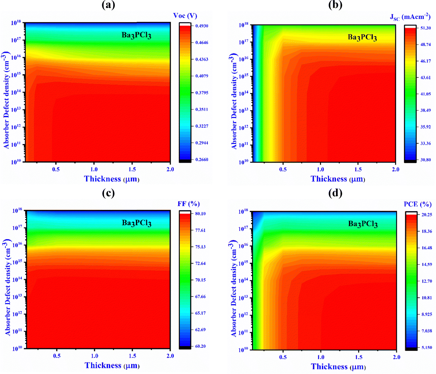
3.7. Impact of device thickness (I, II, III, and IV) and defect density
Fig. 5 displays the impact of the defect density (Nt) on the efficiency of PV cells by illustrating the alterations in both the thickness and the Nt of the Ba3NCl3 absorber layer, varying from 0.1 to 2.0 μm and from 1010 to 1018 cm−3, respectively. The solar cell outcome noticeably deteriorates when the Nt of Ba3NCl3 surpasses 1012 cm−3.68JSC, VOC, PCE and FF for Al/FTO/CdS/Ba3NCl3/Au structures drop from 57 to 32.6 mA cm−2, from 0.63 to 0.14 V, from 31.6% to 3.1%, and from 85.6% to 40%, respectively. As shown in Fig. 5(a), a peak VOC of 0.5 V is obtained if the Nt is kept underneath 1012 cm−3 and the thickness remains less than 1 μm. In contrast, if the Nt goes beyond 1012 cm−3, the VOC decreases markedly to 0.16 V. | ||
| Fig. 5 Influence of variations in absorber thickness and defect density (device-I, Ba3NCl3) on key PV performance factors: (a) VOC, (b) JSC, (c) FF, and (d) PCE. | ||
Fig. 5(b) and (c) indicate that to attain the highest values of JSC and FF of 53.97 mA cm−2 and 82.06%, respectively, the thickness should exceed 1 μm and the Nt should remain below 1012 cm−3. Fig. 5(d) depicts that the highest conversion efficiency, exceeding 23.06%, is obtained once the thickness is within 0.1 to 2.0 μm and the Nt is up to 1012 cm−3. Higher carrier recombination rates, caused by increased defects in the absorber layer, consequently reduce the cell's efficiency.77–79 The optimal criteria for reaching a maximum PCE of 23.06% for device-I have been identified. This involves ensuring an absorber layer thickness of 1.0 μm for Ba3NCl3 with a Nt of 1012 cm−3. With these parameters, the PV cell obtained a VOC of 0.5 V, a JSC of 53.97 mA cm−2, and an FF of 82.06%.
For Al/FTO/CdS/Ba3PCl3/Au (device II) structures, increasing the defect density leads to a decline in JSC, PCE, VOC, and FF, while thickening the absorber layer improves these values. In particular, these parameters increase significantly with a thickness up to 1 μm, beyond which further increases produce only marginal improvements. In contrast, the values drop sharply as the Nt increases up to 1012 cm−3, and any increase beyond this threshold results in a slight decline. Therefore, the optimal absorber layer thickness is 1 μm with a Nt of 1012 cm−3. In these optimal circumstances, JSC, VOC, PCE, and FF reach values of 50.78 mA cm−2, 0.49 V, 19.93%, and 80.01%, respectively. Fig. 6(a) shows that the highest VOC of 0.49 V is gained with a thickness less than 1 μm and a Nt below 1012 cm−3. However, exceeding this defect density threshold significantly reduces the VOC to 0.27 V. Fig. 6(b) and (c) suggest that to achieve the highest JSC and FF values of 50.78 mA cm−2 and 80.01%, the thickness should exceed 1 μm and the Nt should remain below 1012 cm−3. Fig. 6(d) specifies that maintaining a thickness between 0.1 and 2.0 μm and a Nt equal to 1012 cm−3 yields the peak conversion efficiency, surpassing 19.93%.
 | ||
| Fig. 6 Influence of variations in absorber thickness and defect density (device II, Ba3PCl3) on key PV performance factors: (a) VOC, (b) JSC, (c) FF, and (d) PCE. | ||
The FF, JSC, PCE, and VOC of the Al/FTO/CdS/Ba3AsCl3/Au (device III) structures decline significantly from 79.2% to 59%, 47.8 to 29.15 mA cm−2, 18.4% to 5.3%, and 0.49 to 0.3 V, respectively. Fig. 7(a) shows that the peak VOC of 0.47 V is reached when the Nt is underneath 1012 cm−3 and the absorber layer thickness is under 1 μm. When Nt exceeds 1012 cm−3, VOC drops sharply to 0.31 V. Fig. 7(b) and (c) suggest that to obtain the highest values of JSC and FF of 46.76 mA cm−2 and 78.15%, the thickness needs to exceed 1 μm and the Nt should remain under 1012 cm−3. As demonstrated in Fig. 7(d), maintaining a thickness among 0.1 and 2.0 μm and keeping the Nt equal to 1012 cm−3 results in the optimal conversion efficiency, which exceeds 17.12%.
 | ||
| Fig. 7 Influence of variations in absorber thickness and defect density (device-III, Ba3AsCl3) on key PV performance parameters: (a) VOC, (b) JSC, (c) FF, and (d) PCE. | ||
In contrast, the performance metrics of the Al/FTO/CdS/Ba3SbCl3/Au (device IV) structures degrade as the PCE drops from 17.45% to 2.55%, the FF from 76% to 52.4%, the JSC from 47.2 to 28.45 mA cm−2, and the VOC from 0.49 to 0.17 V. Fig. 8(a) shows that the peak VOC of 0.46 V is reached once the Nt is below 1012 cm−3 and the absorber layer thickness is below 1 μm. However, exceeding this Nt threshold significantly reduces the VOC to 0.19 V. Fig. 8(b) and (c) suggest that to achieve the highest JSC and FF values of 45.55 mA cm−2 and 74.49%, the thickness should exceed 1 μm and the Nt should remain under 1012 cm−3. Fig. 8(d) indicates that maintaining a thickness ranging from 0.1 to 2.0 μm and keeping the Nt equal to 1012 cm−3 results in the optimal conversion efficiency, which exceeds 15.71%.
 | ||
| Fig. 8 Influence of variations in absorber thickness and defect density (device-IV, Ba3SbCl3) on key PV performance parameters: (a) VOC, (b) JSC, (c) FF, and (d) PCE. | ||
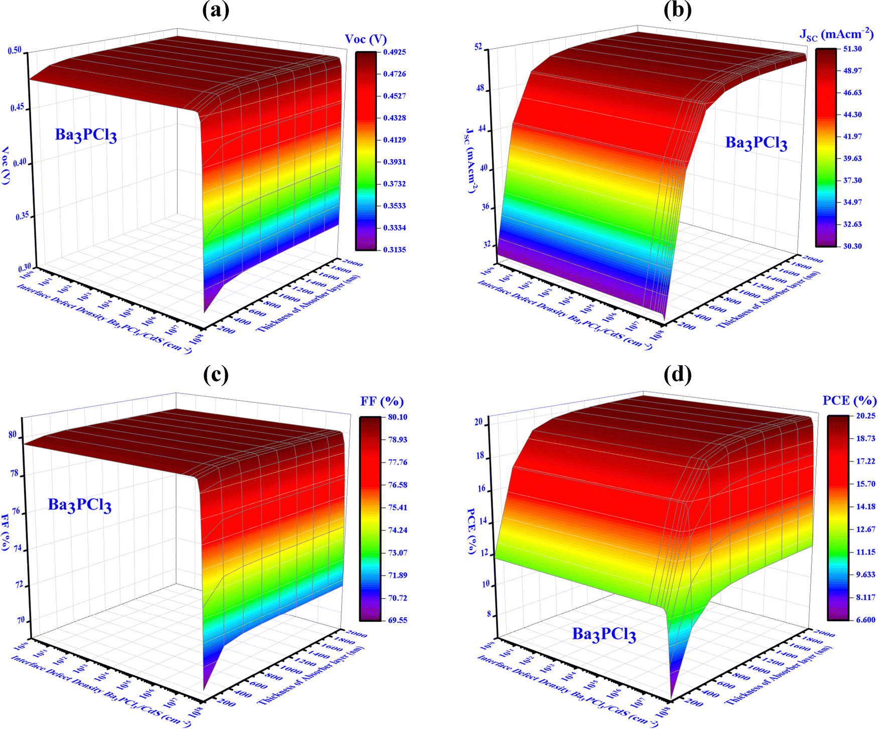
3.8. Impact of device thickness (I, II, III, and IV) and interface change in solar energy efficiency
Fig. 9 presents the influence of Nint on the outcome of photovoltaic cells, illustrating alterations in the Nint as well as the thickness of the Ba3NCl3 absorber layer. These parameters range from 1010 to 1018 cm−3 for defect density and 0.1 to 2.0 μm for thickness. The metrics for solar cell performance reduces significantly if the Nint in the Ba3NCl3 interface exceeds 1012 cm−3. The JSC, VOC, PCE, and FF of Al/FTO/CdS/Ba3NCl3/Au structures reduce from 64.5 to 42 mA cm−2, 0.57 V to 0.15 V, 24.9% to 2.4%, and 77% to 37.8%, respectively. | ||
| Fig. 9 Influence of variations in absorber thickness and defect interface density (device-I, Ba3NCl3) on key PV performance factors: (a) VOC, (b) JSC, (c) FF, and (d) PCE. | ||
Fig. 9(a) shows that the peak VOC of 0.5 V is gained while the absorber layer is 1 μm thick and the Nint is below 1012 cm−3. However, exceeding this threshold of the Nint significantly reduces the VOC to 0.16 V. Fig. 9(b) and (c) indicate that to achieve the peak JSC of 53.97 mA cm−2 and FF of 82.06%, the absorber thickness should be larger than 1 μm, and the Nint should remain below 1012 cm−3. Fig. 9(d) depict that the highest conversion efficiency, surpassing 23.06%, occurs within a thickness ranging from 0.1 to 2.0 μm and when Nint is equal to 1012 cm−3. The addition of high-defect states to the absorber layer boosts carrier recombination, causing a decline in total cell performance.77–79 The best conditions for attaining the peak PCE of 23.06% for device I were identified, which includes a constant Ba3NCl3 absorber thickness of 1.0 μm and an Nint of 1012 cm−3. A VOC of 0.5 V, a JSC of 53.97 mA cm−2, and an FF of 82.06% were achieved by the solar cell in this case.
For Al/FTO/CdS/Ba3PCl3/Au (device II) structures, performance factors such as JSC, PCE, VOC, and FF are negatively impacted by a rise in interface defect density, while an upsurge in the absorber layer's thickness generally improves these values. Up to a thickness of 1 μm, these parameters increase significantly. However, beyond 1 μm, the improvements are marginal. Similarly, these values decrease significantly as the Nint rises up to 1012 cm−3, but the reduction is more gradual once the Nint surpasses 1012 cm−3. Therefore, the optimal thickness is 1 μm, and the ideal Nint is 1012 cm−3. Under these conditions, the PCE is 19.93%, the FF is 80.01%, the JSC is 50.78 mA cm−2, and the VOC is 0.49 V. As illustrated in Fig. 10(a), the peak VOC of 0.49 V is gained with a thickness below 1 μm and a Nint under 1012 cm−3. However, exceeding this interface defect density threshold significantly reduces the VOC to 0.32 V. Fig. 10(b) and (c) indicate that to reach the greatest values of JSC (50.78 mA cm−2) and FF (80.01%), the thickness should be superior to 1 μm and the Nint should not exceed 1012 cm−3. According to Fig. 10(d), maintaining a thickness between 0.1 and 2.0 μm and an Nint equal to 1012 cm−3 results in the optimal conversion efficiency, which exceeds 19.93%.
 | ||
| Fig. 10 Influence of variations in absorber thickness and defect interface density (device-II, Ba3PCl3) on key PV performance factors: (a) VOC, (b) JSC, (c) FF, and (d) PCE. | ||
The JSC, VOC, PCE, and FF of Al/FTO/CdS/Ba3AsCl3/Au (device-III) structures decrease from 47.8 to 28.6 mA cm−2, 0.49 to 0.38 V, 18.4 to 7.8%, and 79.2 to 72.44%, respectively. Fig. 11(a) shows that the peak VOC of 0.47 V is gained if the thickness is below 1 μm and the Nint is under 1012 cm−3. However, exceeding this interface defect density threshold significantly reduces the VOC to 0.39 V. Fig. 11(b) and (c) show that the thickness needs to exceed 1 μm and the Nint should not exceed 1012 cm−3 to attain the peak JSC and FF values of 46.76 mA cm−2 and 78.15%, respectively. Fig. 11(d) shows that a thickness ranging from 0.1 to 2.0 μm and a Nint equal to 1012 cm−3 result in the maximum efficiency, exceeding 17.12%.
 | ||
| Fig. 11 Influence of variations in absorber thickness and defect interface density (device-III, Ba3AsCl3) on key PV performance factors: (a) VOC, (b) JSC, (c) FF, and (d) PCE. | ||
The FF, JSC, PCE, and VOC of the Al/FTO/CdS/Ba3SbCl3/Au (device IV) structures decrease from 76 to 55.8%, 47.2 to 28.15 mA cm−2, 17.45 to 2.6%, and 0.49 to 0.17 V, respectively. Fig. 12(a) shows that the highest VOC of 0.46 V is reached if the thickness is below 1 μm and Nint is under 1012 cm−3. Besides, when the Nint exceeds 1012 cm−3, the VOC noticeably falls into 0.19 V. Fig. 12(b) and (c) indicate that the thickness needs to exceed 1 μm and the Nint should not exceed 1012 cm−3 to achieve the highest JSC and FF values of 45.55 mA cm−2 and 74.49%, respectively. Fig. 12(d) demonstrates that a thickness spanning from 0.1 to 2.0 μm and an Nint equal to 1012 cm−3 result in the utmost efficiency, exceeding 15.71%.
 | ||
| Fig. 12 Influence of variations in absorber thickness and defect interface density (device-IV, Ba3SbCl3) on key PV performance factors: (a) VOC, (b) JSC, (c) FF, and (d) PCE. | ||
As absorber thickness increases, more incident photons are absorbed due to the longer optical path, enhancing light absorption. However, beyond a certain point, further thickness results in only marginal gains, as absorption approaches saturation, consistent with the Beer–Lambert law.80 While thicker layers generate more carriers, they also increase the transport distance, leading to higher recombination, particularly if the carrier diffusion length is shorter than the absorber thickness. This trade-off affects overall efficiency, where thinner layers underperform in photon absorption, and excessively thick layers suffer from recombination losses.81 The optimal thickness, around 1000 nm, strikes a balance between maximizing photon absorption and minimizing recombination. According to Shockley–Read–Hall recombination theory,82 this intermediate thickness offers the highest efficiency by reducing recombination losses while maintaining strong absorption.
3.9. Optimized J–V and QE characteristics
The J–V curves for the device, with optimal parameters (NA of 1016 cm−3, Nint of 1012 cm−2, Nt of 1012 cm−2) and absorber thicknesses between 100 and 2000 nm, are shown in Fig. 13(a). Analysis determined 1000 nm as the ideal absorber thickness, yielding values of (VOC: 0.5 V, JSC: 53.97 mA cm−2, FF: 82.06%), (VOC: 0.49 V, JSC: 50.78 mA cm−2, FF: 80.06%), (VOC: 0.47 V, JSC: 46.76 mA cm−2, FF: 78.15%), and (VOC: 0.46 V, JSC: 45.55 mA cm−2, FF: 74.49%) for devices I, II, III and IV, respectively, with CdS producing the highest PCE. Fig. 13(b) shows the QE curve for absorber thicknesses from 100 to 2000 nm, where QE, the fraction of photogenerated charge carriers per incident photon,83–85 nearly reached saturation at 1000 nm, then rapidly dropped to zero at cutoff wavelengths of 1460, 1330, 1260, and 1240 nm for devices I, II, III and IV, respectively. The 1000-nm thickness was deemed ideal, as supported by the QE spectra and J–V characteristics. | ||
| Fig. 13 (a) J–V and (b) PSC QE curves for devices I, II, III, and IV. | ||
4. Conclusions
This study examines the impact of M-anion modifications on lead-free halide inorganic compounds, specifically Ba3MCl3 (M = N, P, As, Sb), using DFT and SCAPS-1D software. The analysis begins with the use of GGA and PBE functional theory. Band structure and DOS analyses confirm the semiconductor properties of Ba3MCl3 compounds (M = N, P, As, Sb). Optical features such as absorption, dielectric function, electrical conductivity, loss function, reflectance, and refractive index, are explored. ECD mapping reveals the ionic bond nature of these compounds. For the perovskite solar cell, the SCAPS simulator was used to design the structure Al/FTO/CdS/(Ba3NCl3/Ba3PCl3/Ba3AsCl3/Ba3SbCl3)/Au. The simulation results show that Ba3NCl3 delivers the highest JSC, VOC, PCE, and FF values, with 53.97 mA cm−2, 0.5 V, 23.06%, and 82.06%, respectively, outperforming other compounds under similar conditions. In contrast, Ba3SbCl3 exhibits the lowest output values, with JSC of 45.55 mA cm−2, VOC of 0.46 V, PCE of 15.71%, and FF of 74.49%. These results indicate that Ba3MCl3 (M = N, P, As, Sb) compounds have promise for further research in optoelectronic applications.List of abbreviations
| J–V | Current density–voltage |
| N t | Defect density |
| PCE | Power conversion efficiency |
| ECD | Electron charge density |
| SCAPS | Solar cell capacitance simulator |
| J SC | Short circuit current density |
| QE | Quantum efficiency |
| VB | Valence band |
| V OC | Open circuit voltage |
| ETL | Electron transport layer |
| SCF | Self-consistent field |
| DFT | Density functional theory |
| N int | Interface defect density |
| BZ | Brillouin zone |
| FTO | Fluorine-doped tin oxide |
| PSC | Perovskite solar cell |
| FF | Fill factor |
| CB | Conduction band |
| HTL | Hole transport layer |
| WF | Work function |
| PV | Photovoltaic |
Data availability
Data are available from the corresponding author upon reasonable request.Conflicts of interest
The authors have no conflicts of interest.Acknowledgements
A. Irfan extends his appreciation to the Deanship of Research and Graduate Studies at King Khalid University for funding this work through the Large Research Project under grant number RGP2/172/45.References
- S. Marimuthu, S. Pandiaraj, M. Muthuramamoorthy, K. E. Alzahrani, A. N. Alodhayb, S. Pitchaimuthu and A. N. Grace, Experimental and computational DFT, drift-diffusion studies of cobalt-based hybrid perovskite crystals as absorbers in perovskite solar cells, Phys. Chem. Chem. Phys., 2024, 26, 4262–4277 RSC.
- C. Xing, Y. Lei, M. Liu, S. Wu, W. He and Z. Zheng, Environment-friendly Cu-based thin film solar cells: materials, devices and charge carrier dynamics, Phys. Chem. Chem. Phys., 2021, 23, 16469–16487 RSC.
- C. Paduani and A. M. Rappe, Tuning the gap of lead-based halide perovskites by introducing superalkali species at the cationic sites of ABX3-type structure, Phys. Chem. Chem. Phys., 2017, 19, 20619–20626 RSC.
- D. Liu, H. Zeng, H. Peng and R. Sa, Computational study of the fundamental properties of Zr-based chalcogenide perovskites for optoelectronics, Phys. Chem. Chem. Phys., 2023, 25, 13755–13765 RSC.
- Y.-C. Zhao, W.-K. Zhou, X. Zhou, K.-H. Liu, D.-P. Yu and Q. Zhao, Quantification of light-enhanced ionic transport in lead iodide perovskite thin films and its solar cell applications, Light: Sci. Appl., 2017, 6, e16243–e16243 CrossRef CAS PubMed.
- D. Luo, W. Yang, Z. Wang, A. Sadhanala, Q. Hu, R. Su, R. Shivanna, G. F. Trindade, J. F. Watts, Z. Xu, T. Liu, K. Chen, F. Ye, P. Wu, L. Zhao, J. Wu, Y. Tu, Y. Zhang, X. Yang, W. Zhang, R. H. Friend, Q. Gong, H. J. Snaith and R. Zhu, Enhanced photovoltage for inverted planar heterojunction perovskite solar cells, Science, 2018, 360, 1442–1446 CrossRef CAS PubMed.
- H. Bencherif and M. Khalid Hossain, Design and numerical investigation of efficient (FAPbI3)1−x(CsSnI3)x perovskite solar cell with optimized performances, Sol. Energy, 2022, 248, 137–148 CrossRef CAS.
- D. Nadhiya, A. Kala, P. Sasikumar, M. K. A. Mohammed, P. Thirunavukkarasu, M. Prabhaharan, C. Karnan, S. Albukhaty, M. S. Jabir, A. Syed, A. M. Elgorban and N. S. S. Zaghloul, Influence of Cu2+ substitution on the structural, optical, magnetic, and antibacterial behaviour of zinc ferrite nanoparticles, J. Saudi Chem. Soc., 2023, 27, 101696 CrossRef CAS.
- M. Mohammed, A. K. Al-Mousoi, S. M. Majeed, S. Singh, A. Kumar, R. Pandey, J. Madan, D. Ahmed and D. Dastan, Stable Hole-Transporting Material-Free Perovskite Solar Cells with Efficiency Exceeding 14% via the Introduction of a Malonic Acid Additive for a Perovskite Precursor, Energy Fuels, 2022, 36, 13187–13194 CrossRef CAS.
- J. Jiang, Z. Jin, J. Lei, Q. Wang, X. Zhang, J. Zhang, F. Gao and S. (Frank) Liu, ITIC surface modification to achieve synergistic electron transport layer enhancement for planar-type perovskite solar cells with efficiency exceeding 20%, J. Mater. Chem. A, 2017, 5, 9514–9522 RSC.
- F. Meinardi, Q. A. Akkerman, F. Bruni, S. Park, M. Mauri, Z. Dang, L. Manna and S. Brovelli, Doped Halide Perovskite Nanocrystals for Reabsorption-Free Luminescent Solar Concentrators, ACS Energy Lett., 2017, 2, 2368–2377 CrossRef CAS PubMed.
- M. K. A. Mohammed, S. Singh, A. K. Al-Mousoi, R. Pandey, J. Madan, D. Dastan and G. Ravi, Improving the potential of ethyl acetate green anti-solvent to fabricate efficient and stable perovskite solar cells, RSC Adv., 2022, 12, 32611–32618 RSC.
- L. Huxin, X. Liu, X. Gong, R. Zhou, X. Peng, Y. Ouyang, J. Zhuang, H. Li and H. Wang, Multifunctional Additive of Potassium Cinnamate Improve Crystallization and Passivate Defect for Perovskite Solar Cell with Efficiency Exceeding 22\%, Energy Technol., 2022, 10, 2200125 CrossRef.
- M. K. Hossain, G. F. I. Toki, A. Kuddus, M. H. K. Rubel, M. M. Hossain, H. Bencherif, M. F. Rahman, M. R. Islam and M. Mushtaq, An extensive study on multiple ETL and HTL layers to design and simulation of high-performance lead-free CsSnCl3-based perovskite solar cells, Sci. Rep., 2023, 13, 1–24 CrossRef PubMed.
- Z. Shi, J. Guo, Y. Chen, Q. Li, Y. Pan, H. Zhang, Y. Xia and W. Huang, Lead-Free Organic–Inorganic Hybrid Perovskites for Photovoltaic Applications: Recent Advances and Perspectives, Adv. Mater., 2017, 29, 1605005 CrossRef PubMed.
- X. Meng, Y. Wang, J. Lin, X. Liu, X. He, J. Barbaud, T. Wu, T. Noda, X. Yang and L. Han, Surface-Controlled Oriented Growth of FASnI3 Crystals for Efficient Lead-free Perovskite Solar Cells, Joule, 2020, 4, 902–912 CrossRef CAS.
- G. Schileo and G. Grancini, Lead or no lead? Availability, toxicity, sustainability and environmental impact of lead-free perovskite solar cells, J. Mater. Chem. C, 2021, 9, 67–76 RSC.
- N. Pandit, R. Singh, T. K. Joshi, A. Shukla, P. K. Kamlesh, A. Dubey, T. Kumar, M. S. Chauhan and A. S. Verma, Investigation of a potential photovoltaic absorber based on first principles spectroscopic screening of chalcogenide perovskites: CaZrX3 (X = S, Se), J. Comput. Electron., 2024, 24, 11 CrossRef.
- N. Pandit, R. Singh, P. K. Kamlesh, N. Kumar, P. Sharma, S. Kumari, T. Kumar, S. Al-Qaisi and A. S. Verma, Study of chalcogenide-based metal perovskites BaZrX3 (X = S and Se): DFT insight into fundamental properties for sustainable energy generation using AMPS-1D, J. Comput. Electron., 2024, 23, 1014–1028 CrossRef CAS.
- N. Pandit, R. Singh, A. Kumar, T. K. Joshi, A. Shukla, U. Rani, P. K. Kamlesh, T. Kumar, Priyanka and A. S. Verma, Physical properties and power conversion efficiency of SrZrX3 (X = S and Se) chalcogenide perovskite solar cell, Mod. Phys. Lett. B, 2024, 38, 2450345 CrossRef CAS.
- S. Kumari, U. Rani, M. Rani, R. Singh, P. K. Kamlesh, S. Kumari, T. Kumar and A. S. Verma, Computational investigation of the fundamental physical properties of lead-free halide double perovskite Rb2NaCoX6 (X = Cl, Br, and I) materials: potential prospects for sustainable energy, Mod. Phys. Lett. B, 2024, 38, 2450323 CrossRef CAS.
- N. Pandit, A. Dubey, T. K. Joshi, A. Shukla, U. Rani, P. K. Kamlesh, R. Gupta, T. Kumar, K. Kaur and A. S. Verma, Effect of anion (S2− & Se2−) replacement on photovoltaic properties in transition metal (Ba-Barium) chalcogenide perovskites, Int. J. Mod. Phys. B, 2024, 2550059 Search PubMed.
- H. Park, R. Mall, F. H. Alharbi, S. Sanvito, N. Tabet, H. Bensmail and F. El-Mellouhi, Exploring new approaches towards the formability of mixed-ion perovskites by DFT and machine learning, Phys. Chem. Chem. Phys., 2019, 21, 1078–1088 RSC.
- Y. Zhou and A. Gray-Weale, A numerical model for charge transport and energy conversion of perovskite solar cells, Phys. Chem. Chem. Phys., 2016, 18, 4476–4486 RSC.
- Y.-Q. Zhao, Q.-R. Ma, B. Liu, Z.-L. Yu and M.-Q. Cai, Pressure-induced strong ferroelectric polarization in tetra-phase perovskite CsPbBr3, Phys. Chem. Chem. Phys., 2018, 20, 14718–14724 RSC.
- M. F. Rahman, M. M. Islam, M. R. Islam, A. Ghosh, M. A. Rahman, M. H. Rahman, M. A. I. Islam, M. A. Islam, H. Albalawi and Q. Mahmood, An investigation on strain-incited electronic and optical properties of novel inorganic cubic material Sr3AsCl3, J. Solid State Chem., 2023, 328, 124341 CrossRef CAS.
- M. F. Rahman, M. H. Rahman, M. R. Islam, M. K. Hossain, A. Ghosh, M. S. Islam, M. M. Islam, M. Harun-Or-Rashid, H. Albalawi and Q. Mahmood, The optical and electronic properties of inorganic halide perovskite Sr3NCl3 under applied biaxial strain, J. Mater. Sci., 2023, 58, 13100–13117 CrossRef CAS.
- M. F. Rahman, M. A. I. Islam, M. R. Islam, M. H. Ali, P. Barman, M. A. Rahman, M. Harun-Or-Rashid, M. Hasan and M. K. Hossain, Investigation of a novel inorganic cubic perovskite Ca3PI3 with unique strain-driven optical, electronic, and mechanical properties, Nano Select, 2023, 4, 632–645 CrossRef CAS.
- M. F. Rahman, M. A. Rahman, M. R. Islam, A. Ghosh, M. A. Bashar Shanto, M. Chowdhury, M. Al Ijajul Islam, M. H. Rahman, M. K. Hossain and M. A. Islam, Unraveling the strain-induced and spin-orbit coupling effect of novel inorganic halide perovskites of Ca3AsI3 using DFT, AIP Adv., 2023, 13, 085329 CrossRef CAS.
- A. Ghosh, M. F. Rahman, M. R. Islam, M. S. Islam, M. Amami, M. K. Hossain and A. B. Md Ismail, Inorganic novel cubic halide perovskite Sr3AsI3: strain-activated electronic and optical properties, Heliyon, 2023, 9, e19271 CrossRef CAS PubMed.
- C. Hadenfeldt and H. O. Vollert, Darstellung, thermisches Verhalten und Kristallstruktur des Calciumarsenidchlorids Ca3AsCl3, J. Inorg. Gen. Chem., 1982, 491, 113–118 CAS.
- C. Hadenfeldt and H. Herdejürgen, Darstellung, kristallstruktur und thermisches verhalten der calciumphosphidchloride Ca2−xP1−xCl1+x (0 ≤ x ≤ 0.18) und Ca3PCl3, J. Less-Common Met., 1986, 124, 93–103 CrossRef CAS.
- V. C. Hadenfeldt and W. Fester, Reindarstellung und thermische Stabilitat von Calcium-phosphid- und -arsenidiodiden: Ca, PI, Ca, AsI, Ca, PI und Ca, Asl, Anorg. Chem., 1982, 30, 25–30 CrossRef.
- S. Andersson, Magnesium nitride fluorides, J. Solid State Chem., 1970, 1, 306–309 CrossRef.
- C. Hadenfeldt and P. Schulz, Darstellung, Struktur und Temperaturabhängigkeit der Phasenbreite der Phase Ca2−xAs1−xBr1+x und thermisches Verhalten der Verbindung Ca3AsBr3, J. Inorg. Gen. Chem., 1984, 518, 77–86 CAS.
- D. A. Dixon, in Encyclopedia of Geochemistry, ed. W. M. White, Springer International Publishing, Cham, 2016, pp. 1–7 Search PubMed.
- M. H. K. Rubel, M. A. Hossain, M. K. Hossain, K. M. Hossain, A. A. Khatun, M. M. Rahaman, M. Ferdous Rahman, M. M. Hossain and J. Hossain, First-principles calculations to investigate structural, elastic, electronic, thermodynamic, and thermoelectric properties of CaPd3B4O12 (B = Ti, V) perovskites, Results Phys., 2022, 42, 105977 CrossRef.
- M. F. Rahman, M. N. H. Toki, M. R. Islam, P. Barman, S. Chowdhury, M. Rasheduzzaman and M. Z. Hasan, A computational study of electronic, optical, and mechanical properties of novel Ba3SbI3 perovskite using DFT, Opt. Quantum Electron., 2023, 56, 206 CrossRef.
- M. Ferdous Rahman, P. Barman, M. Azizur Rahman, M. Mushtaq, M. Rasidul Islam, M. Atikur Rahman, M. Z. Sultan, A. R. Chaudhry and A. Irfan, Electronic, optical, thermophysical, and mechanical properties of lead-free Ba3SbBr3 perovskite, Polyhedron, 2024, 254, 116937 CrossRef CAS.
- Q. Wang, W. Yu, X. Fu, C. Qiao, C. Xia and Y. Jia, Electronic and magnetic properties of SnSe monolayers doped by Ga, In, As, and Sb: a first-principles study, Phys. Chem. Chem. Phys., 2016, 18, 8158–8164 RSC.
- M. Faizan, J. Xie, G. Murtaza, C. Echeverría-Arrondo, T. Alshahrani, D. Bhamu, A. Laref, I. Seró and S. Khan, A first-principle study of the stability, electronic structure, and optical properties of halide double perovskite Rb2Sn1−xTexI6 for solar cell applications, Phys. Chem. Chem. Phys., 2023, 23, 4646–4657 RSC.
- M. D. Segall, P. J. D. Lindan, M. J. Probert, C. J. Pickard, P. J. Hasnip, S. J. Clark and M. C. Payne, First-principles simulation: ideas, illustrations and the CASTEP code, J. Phys.: Condens. Matter, 2002, 14, 2717–2744 CrossRef CAS.
- W. Kohn and L. J. Sham, Self-Consistent Equations Including Exchange and Correlation Effects, Phys. Rev. A: At., Mol., Opt. Phys., 1965, 140, 1133 CrossRef.
- G. P. Francis and M. C. Payne, Finite basis set corrections to total energy pseudopotential calculations, J. Phys.: Condens. Matter, 1990, 2, 4395–4404 CrossRef.
- T. H. Fischer and J. Almlöf, General methods for geometry and wave function optimization, J. Phys. Chem., 1992, 96, 9768–9774 CrossRef CAS.
- J. P. Perdew, K. Burke and M. Ernzerhof, Generalized Gradient Approximation Made Simple, Phys. Rev. Lett., 1996, 77, 3865–3868 CrossRef CAS PubMed.
- H. J. Monkhorst and J. D. Pack, Special points for Brillonin-zone integrations, Phys. Rev. B: Condens. Matter Mater. Phys., 1976, 13, 5188 CrossRef.
- M. H. Rahman, H. Full, M. A. Rahman, S. R. Al Ahmed, L. Ben Farhat, S. Ezzine and M. F. Rahman, ETL engineering in lead-free new Ca3PBr3 perovskite type structure of anti-perovskite derivative material for stable and effective photovoltaic solar cells, New J. Chem., 2025, 49, 3044–3066 RSC.
- S. Bhattacharyya and A. K. Singh, Semiconductor–metal transition in semiconducting bilayer sheets of transition-metal dichalcogenides, Phys. Rev. B: Condens. Matter Mater. Phys., 2012, 86, 1–7 Search PubMed.
- W.-J. Yin, J.-H. Yang, J. Kang, Y. Yan and S.-H. Wei, Halide perovskite materials for solar cells: a theoretical review, J. Mater. Chem. A, 2015, 3, 8926–8942 RSC.
- D.-Y. Chen, Y. Wu, L. Jin, Y. Li, X. Wang, J. Duan, J. Han, X. Li, Y.-Z. Long, X. Zhang, D. Chen and B. Teng, Superconducting properties in a candidate topological nodal line semimetal SnTaS2 with a centrosymmetric crystal structure, Phys. Rev. B, 2019, 100, 64516 CrossRef CAS.
- M. Petrović, V. Chellappan and S. Ramakrishna, Perovskites: solar cells & engineering applications – materials and device developments, Sol. Energy, 2015, 122, 678–699 CrossRef.
- M. A. Islam, M. Z. Rahaman and S. K. Sen, A comparative study of hydrostatic pressure treated environmentally friendly perovskites CsXBr3 (X = Ge/Sn) for optoelectronic applications, AIP Adv., 2021, 11, 075109 CrossRef CAS.
- M. A. Islam, J. Islam, M. N. Islam, S. K. Sen and A. K. M. A. Hossain, Enhanced ductility and optoelectronic properties of environment-friendly CsGeCl3 under pressure, AIP Adv., 2021, 11, 45014 CrossRef CAS.
- S. ur Rehman, F. K. Butt, Z. Tariq, F. Hayat, R. Gilani and F. Aleem, Pressure induced structural and optical properties of cubic phase SnSe: an investigation for the infrared/mid-infrared optoelectronic devices, J. Alloys Compd., 2017, 695, 194–201 CrossRef CAS.
- F. Ahmad, A. Lakhtakia and P. B. Monk, Double-absorber thin-film solar cell with 34% efficiency, Appl. Phys. Lett., 2020, 117, 33901 CrossRef CAS.
- D. Tsukahara, S. Yachi, H. Takeuchi, R. Takabe, W. Du, M. Baba, Y. Li, K. Toko, N. Usami and T. Suemasu, p-BaSi2/n-Si heterojunction solar cells with conversion efficiency reaching 9.0%, Appl. Phys. Lett., 2016, 108, 152101 CrossRef.
- G. Yu, C. H. Lee, A. J. Heeger and S.-W. Cheong, Photoconductivity and optical conductivity in lightly doped Nd2CuO4−δ, Phys. C, 1992, 203, 419–425 CrossRef CAS.
- M. A. Ali, N. Alam, S. Ali, S. A. Dar, A. Khan, G. Murtaza and A. Laref, A theoretical study of the structural, thermoelectric, and spin-orbit coupling influenced optoelectronic properties of CsTmCl3 halide perovskite, Int. J. Quantum Chem., 2020, 120, 1–9 Search PubMed.
- M. A. Ali, R. Ullah, S. Murad, S. A. Dar, A. Khan, G. Murtaza and A. Laref, Insight into pressure tunable structural, electronic and optical properties of via DFT calculations, Eur. Phys. J. Plus, 2020, 135, 309 CrossRef.
- X. Liu, B. Xie, C. Duan, Z. Wang, B. Fan, K. Zhang, B. Lin, F. J. M. Colberts, W. Ma, R. A. J. Janssen, F. Huang and Y. Cao, A high dielectric constant non-fullerene acceptor for efficient bulk-heterojunction organic solar cells, J. Mater. Chem. A, 2018, 6, 395–403 RSC.
- S. Saha, T. P. Sinha and A. Mookerjee, Electronic structure, chemical bonding, and optical properties of paraelectric BaTiO3, Phys. Rev. B: Condens. Matter Mater. Phys., 2000, 62, 8828–8834 CrossRef CAS.
- M. M. Rahaman, M. H. K. Rubel, M. A. Rashid, M. A. Alam, K. M. Hossain, M. I. Hossain, A. A. Khatun, M. M. Hossain, A. K. M. A. Islam, S. Kojima and N. Kumada, Mechanical, electronic, optical, and thermodynamic properties of orthorhonmbic LiCuBiO4 crystal: a first-priciples study, J. Mater. Res. Technol., 2019, 8, 3783–3794, DOI:10.1016/j.jmrt.2019.06.039.
- M. Roknuzzaman, K. (Ken) Ostrikov, K. Chandula Wasalathilake, C. Yan, H. Wang and T. Tesfamichael, Insight into lead-free organic-inorganic hybrid perovskites for photovoltaics and optoelectronics: a first-principles study, Org. Electron., 2018, 59, 99–106 CrossRef CAS.
- M. Burgelman, P. Nollet and S. Degrave, Modelling polycrystalline semiconductor solar cells, Thin Solid Films, 2000, 361–362, 527–532 CrossRef CAS.
- M. A. Ghebouli, B. Ghebouli, R. Larbi, T. Chihi and M. Fatmi, Effect of buffer nature, absorber layer thickness and temperature on the performance of CISSe based solar cells, using SCAPS-1D simulation program, Optik, 2021, 241, 166203 CrossRef CAS.
- A. Kuddus, M. F. Rahman, S. Ahmmed, J. Hossain and A. B. M. Ismail, Role of facile synthesized V2O5 as hole transport layer for CdS/CdTe heterojunction solar cell: validation of simulation using experimental data, Superlattices Microstruct., 2019, 132, 106168 CrossRef CAS.
- U. Mandadapu, Simulation and Analysis of Lead based Perovskite Solar Cell using SCAPS-1D, Indian J. Sci. Technol., 2017, 10, 1–8 CrossRef.
- L. Lin, L. Jiang, P. Li, B. Fan and Y. Qiu, A modeled perovskite solar cell structure with a Cu2O hole-transporting layer enabling over 20% efficiency by low-cost low-temperature processing, J. Phys. Chem. Solids, 2019, 124, 205–211 CrossRef CAS.
- I. Alam, R. Mollick and M. A. Ashraf, Numerical simulation of Cs2AgBiBr6-based perovskite solar cell with ZnO nanorod and P3HT as the charge transport layers, Phys. B, 2021, 618, 413187 CrossRef CAS.
- A. Bag, R. Radhakrishnan, R. Nekovei and R. Jeyakumar, Effect of absorber layer, hole transport layer thicknesses, and its doping density on the performance of perovskite solar cells by device simulation, Sol. Energy, 2020, 196, 177–182 CrossRef CAS.
- D. E. Tareq, S. M. AbdulAlmohsin and H. H. Waried, Efficiency of TiO2/Peroviskites/Cu2O Solar Cells with Optimal Thickness at Varying of Environment Temperature, IOP Conf. Ser.: Mater. Sci. Eng., 2020, 928, 072044 CAS.
- D. Liu, M. K. Gangishetty and T. L. Kelly, Effect of CH3NH3PbI3 thickness on device efficiency in planar heterojunction perovskite solar cells, J. Mater. Chem. A, 2014, 2, 19873–19881 RSC.
- P. K. Patel, Device simulation of highly efficient eco-friendly CH3NH3SnI3 perovskite solar cell, Sci. Rep., 2021, 11, 3082 CrossRef CAS PubMed.
- A. Tara, V. Bharti, S. Sharma and R. Gupta, Device simulation of FASnI3 based perovskite solar cell with Zn(O0.3, S0.7) as electron transport layer using SCAPS-1D, Opt. Mater., 2021, 119, 111362 CrossRef CAS.
- K. D. Jayan and V. Sebastian, Comparative performance analysis of mixed halide perovskite solar cells with different transport layers and back metal contacts, Semicond. Sci. Technol., 2021, 36, 065010 CrossRef CAS.
- M. Samiul Islam, K. Sobayel, A. Al-Kahtani, M. A. Islam, G. Muhammad, N. Amin, M. Shahiduzzaman and M. Akhtaruzzaman, Defect Study and Modelling of SnX3-Based Perovskite Solar Cells with SCAPS-1D, Nanomaterials, 2021, 11, 1218 CrossRef PubMed.
- G. K. Gupta, A. Garg and A. Dixit, Electrical and impedance spectroscopy analysis of sol–gel derived spin coated Cu2ZnSnS4 solar cell, J. Appl. Phys., 2018, 123, 013101 CrossRef.
- F. Ferdiansjah and K. Tirtakusuma Mularso, Analysis of Back Surface Field (BSF) Performance in P-Type And N-Type Monocrystalline Silicon Wafer, E3S Web Conf., 2018, 43, 01006 CrossRef.
- M. A. Green, K. Emery, Y. Hishikawa, W. Warta and E. D. Dunlop, Solar cell efficiency tables (Version 45), Prog. Photovoltaics Res. Appl., 2015, 23, 1–9 CrossRef.
- S. Rühle, Tabulated values of the Shockley–Queisser limit for single junction solar cells, Sol. Energy, 2016, 130, 139–147 CrossRef.
- W. Shockley and W. T. Read, Statistics of the Recombinations of Holes and Electrons, Phys. Rev., 1952, 87, 835–842 CrossRef CAS.
- G. E. Eperon, G. M. Paternò, R. J. Sutton, A. Zampetti, A. A. Haghighirad, F. Cacialli and H. J. Snaith, Inorganic caesium lead iodide perovskite solar cells, J. Mater. Chem. A, 2015, 3, 19688–19695 RSC.
- J. Hossain, M. M. A. Moon, B. K. Mondal and M. A. Halim, Design guidelines for a highly efficient high-purity germanium (HPGe)-based double-heterojunction solar cell, Opt. Laser Technol., 2021, 143, 107306 CrossRef CAS.
- M. M. A. Moon, M. H. Ali, M. F. Rahman, A. Kuddus, J. Hossain and A. B. M. Ismail, Investigation of thin-film p-BaSi2/n-CdS heterostructure towards semiconducting silicide based high efficiency solar cell, Phys. Scr., 2020, 95, 035506 CrossRef CAS.
| This journal is © the Owner Societies 2025 |