Electronic and optical properties in helical trilayer graphene under compression†
Received
24th January 2025
, Accepted 8th May 2025
First published on 15th May 2025
Abstract
We built three periodic structures of high-angle helical trilayer graphene (hTLG-1, hTLG-2, and hTLG-3) with a relative interlayer rotation angle (θ = 21.78°) and different initial vertical stacking (locally a C6 or C3 symmetry) between consecutive bilayers. Two-dimensional (2D) real-space moiré patterns and the corresponding calculated diffraction patterns showed symmetry differences between the periodic structures. Once the atomic models were characterized in both real and reciprocal spaces, the electronic and linear optical properties of these hTLG systems were studied using density functional theory (DFT) calculations and interlayer compression (δ) as an additional degree of freedom. The electronic band structures and total density of states (DOS), the real part of in-plane 2D linear optical conductivity (Re[σ2D]), and optical absorption (α) properties were studied. The electronic properties revealed an electron–hole asymmetry around the Fermi energy at different δ values, although strong hole localization at high compression (δ ≤ −19%) was obtained. Indeed, we found high Re[σ2D] values: Re[σ2D(ħω = 90 meV)] ∼ 9.5σ0, Re[σ2D(ħω = 65 meV)] = 18σ0, and Re[σ2D(ħω = 170 meV)] = 10σ0 for the hTLG-1, hTLG-2 and hTLG-3, respectively, when δ = −21.6%. σ0 = e2π/2h, is the optical conductivity of monolayer graphene. In addition, an α enhancement in the visible spectrum was obtained. These results demonstrate the relevance of the initial vertical stacking and interlayer compression on the electronics and optics of hTLG superlattices.
1. Introduction
Graphene has been a cornerstone in the field of nanomaterials since its discovery that is known for its extraordinary electrical, mechanical, and thermal properties. The discovery of superconductivity in twisted bilayer graphene (tBLG), among other interesting phenomena such as correlated insulating states, orbital magnetism, and resonating valence bond states,1–7 has sparked interest in exploring other geometric arrangements of graphene. The aforementioned physical phenomena have been ascribed to nearly flat electronic bands positioned at the Fermi energy.8–11 Subsequently, similar phenomena were observed in twisted trilayer graphene (tTLG)12–15 and twisted multilayer graphene (tMLG) systems.16,17 Some researchers believe that these systems represent the beginning of a new era in materials science,18,19 since these layered and twisted van der Waals homostructures belong to a new group of quantum nanomaterials. Currently, the configuration of multilayered systems with properties different from those of monolayer graphene is one of the current research topics. Among these configurations, helical trilayer graphene (hTLG) is a fascinating structure owing to its unique electron correlation and optical properties.20–23 The hTLG consists of three graphene layers, with the top and bottom layers twisted relative to the middle layer at specific angles. A variant of three-layer graphene, hTLG, introduces an additional degree of freedom, namely, helical layering. This arrangement creates a periodic moiré pattern, which becomes a new degree of freedom that allows us to manipulate the electronic band structures and optical response such that it is not involved in either the monolayer or the bilayer.
In twisted graphene systems, the interlayer rotation angle (θ) is an adjustable parameter for tuning physical properties. However, from an ab initio perspective, the study of electronic properties, for example, for twisted systems with low or marginal angles is limited by practical computational resources. This is because the low θ values imply the presence of several thousands atoms.24 Hence, as an alternative to θ, external hydrostatic pressure is a prominent auxiliary variable in experimental and first-principles studies.25,26 The effects of pressure on the Fermi level position, charge carrier mobility, topological transitions, and electronic phase transitions in tBLG have been demonstrated in recent theoretical and experimental studies.2,27–35 By applying external pressure to the hTLG structure, the interlayer distance can be set, which significantly affects the electronic interactions between the layers. This ability to tailor the effects of pressure is suitable for controlling the electronic and optical properties of hTLG systems, thus turning them into versatile platforms for studying various phenomena ranging from superconductivity and magnetism to advanced optical electronics. Nonetheless, it is worth noting that as in bulk-graphite with AA or AB (Bernal) stacking, the low-energy electronic properties are different36; moreover, the low-energy spectrum is different in tBLG systems because of the initial vertical stacking.37,38 Vertical stacking in tBLG systems is termed sub-lattice exchange parity with C6 or C3 rotation symmetry. The electronic and optical properties of high-angle tBLG have a sublattice exchange parity dependence as shown by Talkington and Mele in ref. 39 and 40.
In this paper, we present a theoretical study of the electronic and optical properties of high-angle commensurate hTLG using total energy density functional theory (DFT) calculations. We built a minimal periodic structure of hTLG with θ = 21.78° between consecutive bilayers and counter-clockwise helicity. Here, we consider the interlayer compression, δ, and the local sublattice-exchange parity C6 or C3,37–40 as two additional degrees of freedom to tune the electronic and optical properties of the hTLG. This shows that: (1) the external pressure is a versatile control knob for tuning the electronic properties instead of θ, and (2) the initial sub-lattice exchange parity between layers is useful for differentiating among hTLG structures and tuning the electronic and optical properties at high pressure. The outline of this paper is as follows: the computational methodology is presented in Section 2, the results and discussion are presented in Section 3, and the conclusions of the results are provided in Section 4.
2. Computational methodology
The ground-state structural, electronic, and optical properties were calculated using the DFT formalism implemented in the SIESTA code.41,42 The electron exchange–correlation effects were described with a generalized gradient approximation (GGA) following the Perdew–Burke–Ernzerhof (PBE) parametrization,43 meanwhile, electron–ion interactions were treated with norm-conserving Trouiller-Martins pseudopotentials.44 Because SIESTA uses a linear combination of numerical pseudoatomic orbitals (LCAO), we employed an optimized single-ζ polarized (SZP) basis set to expand the Kohn–Sham wavefunctions with an energy mesh-cutoff of 350 Ry. The structural parameters and forces were converged using a Γ-centered 27 × 27 × 1 Monkhorst–Pack k-grid.45 An electronic temperature of 10 K was used for Fermi surface broadening. The atomic positions were optimized until the residual forces were 5 meV Å−1 or less, with a threshold value for electronic self-consistency of 10−4 eV. To simulate hTLG as a slab, we employed the supercell (SC) method with a vacuum space of 20 Å between adjacent graphene monolayers. The atomic models were visualized using VESTA software.46
3. Results and discussion
3.1. Real and reciprocal space
The optimized hexagonal crystal structure of monolayer graphene is represented by the following three optimized lattice parameters:
| aG = 2.46 Å, bG = 2.46 Å, cG = 30.00 Å, |
| | |
α = 90°, β = 90°, γ = 120°.
| (1) |
To build the hTLG systems with local even (C6 in-plane axis rotation symmetry) or odd (C3 in-plane axis rotation symmetry) initial stackings in the AA regions of moiré patterns, we employed Nook-iin software47 with the following two carbon atomic bases in fractional coordinates:
| CA = (1/3, 2/3, 0), CB = (2/3, 1/3, 0), |
| | |
CA′ = (1/3, 2/3, 0), CB′ = (0, 0, 0),
| (2) |
and the procedure described in ref.
24,
26,
48 and
49 for the highest commensurable angle of
θ = 21.78°. Fig. S1 of the ESI,
† shows real space representations of the graphene monolayer with the atomic basis defined in
eqn (2). The tBLG with different AA, AB or BA regions owing to different initial stackings are shown in Fig. S2 of the ESI.
† The green, blue, and red spheres in
Fig. 1 represent the top, middle, and bottom graphene monolayers, respectively. We labeled three different atomic configurations: hTLG-1, hTLG-2, and hTLG-3, which correspond to even–even, even–odd, and odd–odd parities between consecutive pairs of layers. For example, the hTLG-1 system has an even parity between the green and blue layers, and the same even parity is maintained between the blue and red layers. This was observed in the regions with AA stacking at the corners of the hexagonal lattice, as shown in
Fig. 1 and Fig. S3(a) of the ESI.
† VESTA software can be used to obtain the lattice vectors and atomic basis of the three layers using the following transformation matrix:
48,49| |
 | (3) |
The
m and
n integer values used in
eqn (3):
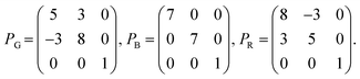
PG(5,3),
PB(7,0) and
PR(8, −3) for the green, blue, and red layers, respectively, were obtained using Nook-iin software.
47 These three transformation matrices ensure the same
θ value between consecutive bilayers. Thus, the transformation matrices are as follows:
| |
 | (4) |
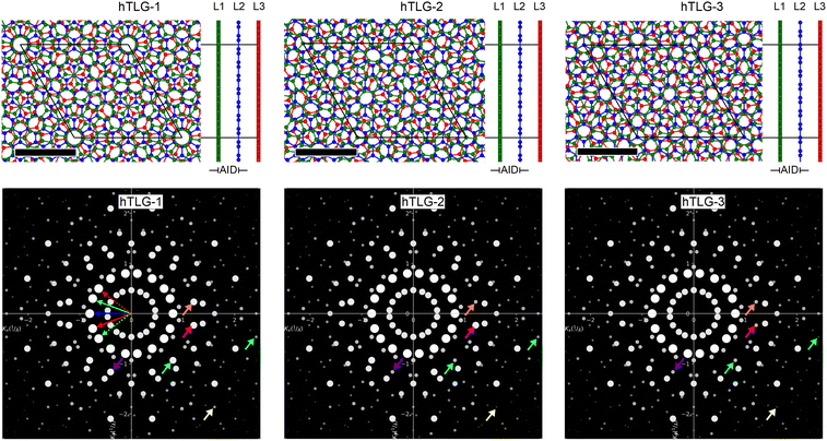 |
| | Fig. 1 Top panels: Top and side views of hTLG systems with θ = 21.78° between consecutive bilayers. Black lines delimit the periodic cell. Black scale bar, 10 Å. Green, blue, and red spheres represent carbon atoms at the top (L1), middle (L2), and bottom (L3) graphene layer. The average interlayer distance (AID) is defined between the L1 and L2 graphene layers. Bottom panels: Calculated diffraction patterns projected on the (001) plane. Small colored arrows denote diffraction spots for comparison among three structures. While large red, blue and green arrows pointing from the origin are steers to observe different relative orientations between consecutive layers. All the white spots are normalized to the diffraction spot with the second highest intensity. Scale in Å−1. | |
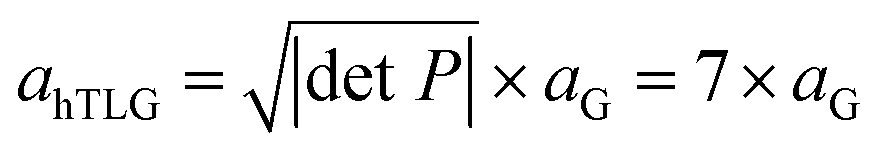
To construct the hTLG-1 system shown in Fig. 1, we used the lattice parameters in eqn (1), the first atomic bases CA and CB of eqn (2), and the transformation matrices in eqn (4) for every graphene layer in the VESTA software.46 For the hTLG-2 system, we used the same lattice parameters as those in eqn (1), but with the CA and CB, CA and CB, and CA′ and CB′ atomic bases for the red, blue, and green layers of eqn (2) and the same transformation matrix for each system in eqn (4). The last configuration hTLG-3 was set with the CA and CB, CA′ and CB′, and CA and CB basis for the red, blue, and green layers in eqn (2), respectively, and the transformation matrix for each graphene layer in eqn (4). Using the P matrices in eqn (4), the lattice parameter of hTLG is  . Additionally, the |det
![[thin space (1/6-em)]](https://www.rsc.org/images/entities/char_2009.gif) P| yields the same number of graphene unit cells inside the SC, that is, 49 unit cells. The three structures shown in Fig. 1 comprise 294 carbon atoms. These are the smallest helical structures that can be studied using DFT formalism implemented in the SIESTA package. We built other periodic structures with angles ranging from 8° to 30°, but the number of atoms was greater than 1800. See the plot and table in Fig. S3(b) of the ESI.† These structures are challenging to study numerically with DFT especially the physical properties like the linear optical properties as the optical conductivity, σ2D. Thus, our study focused on the smallest periodic trilayer graphene owing to the limited computational resources. Notably, the transformation matrices in eqn (4) can be used to build other periodic helical homostructures. For example, hexagonal boron nitride (hBN) and transition metal dichalcogenides (TMDCs) layers. Indeed, this hTLG system is a minimally twisted, helical, and commensurable structure with null strain along the lattice vectors, as a result of using the Nook-iin software.47
P| yields the same number of graphene unit cells inside the SC, that is, 49 unit cells. The three structures shown in Fig. 1 comprise 294 carbon atoms. These are the smallest helical structures that can be studied using DFT formalism implemented in the SIESTA package. We built other periodic structures with angles ranging from 8° to 30°, but the number of atoms was greater than 1800. See the plot and table in Fig. S3(b) of the ESI.† These structures are challenging to study numerically with DFT especially the physical properties like the linear optical properties as the optical conductivity, σ2D. Thus, our study focused on the smallest periodic trilayer graphene owing to the limited computational resources. Notably, the transformation matrices in eqn (4) can be used to build other periodic helical homostructures. For example, hexagonal boron nitride (hBN) and transition metal dichalcogenides (TMDCs) layers. Indeed, this hTLG system is a minimally twisted, helical, and commensurable structure with null strain along the lattice vectors, as a result of using the Nook-iin software.47
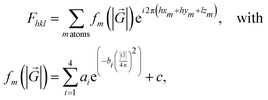
With the atomic models forming moiré patterns in the real space in Fig. 1, owing to the superposition of the three monolayers, the observation of symmetries or local differences between structures is rather difficult. An alternative to discerning the possible symmetries in these hTLG structures is their reciprocal space representation as diffraction patterns (see the bottom panels in Fig. 1). Hence, we plot the reciprocal space of periodic hTLG systems; for each reciprocal lattice point, we calculate its intensity value, I, using the corresponding structure factor, Fhkl, as I = |Fhkl|2. Fhkl is a function of the atomic form factor, fm(|![[G with combining right harpoon above (vector)]](https://www.rsc.org/images/entities/i_char_0047_20d1.gif) |). For every reciprocal lattice point,
|). For every reciprocal lattice point,
| |
 | (5) |
where
h,
k, and
l are the Miller integer indices, and
xm,
ym, and
zm are the fractional coordinates of the atomic basis. We considered that the electron density is spherically symmetric such that the value of the Fourier transform,
fm, solely depends on the distance, |
|, from the origin in reciprocal space.
50 The constants
ai,
bi, and
c for carbon atoms,
a1 = 2.31,
b1 = 20.8439,
a2 = 1.02,
b2 = 10.2075,
a3 = 1.5886,
b3 = 0.5687,
a4 = 0.865,
b4 = 51.6512 and
c = 0.2156 were taken from ref.
50. The size symbol of the circles is proportional to the
I of the spots in
Fig. 1. The
I value for all the peaks was normalized to the second maximum intensity value using 100 Miller indices. Because the diffraction spots are represented in 2D, we set the
l = 0 in
eqn (5), to avoid the slab thickness problem in the hTLG system.
In general, at the equilibrium average interlayer distance (AID) of AID0 = 3.235 Å, the diffraction patterns show a set of 18 small spots surrounding the origin (Γ point) in reciprocal space. This is because there are three graphene layers with six rotational symmetries. The second set of diffraction spots is more intense than that of the first set, but it reveals an interlayer relative orientation difference between the consecutive layers. This is depicted by the large colored arrows in the hTLG-1 configuration, starting from the origin. The interlayer angles between red and blue and the blue and green arrows are the same, θ = 21.78°. However, the angle between the dashed green arrow and its neighboring red arrow (equal to the angle between the green arrow and its neighboring dashed red arrow) is small and equal to (360° − 12 × 21.78°)/6 = 16.44°. A smaller interlayer angle lies between the outermost green and red graphene layers. To be precise, an interlayer angle of 16.44° is also commensurable and is the same angle found when a graphene bilayer is built with integer pairs (m,n) = (5,3) as in ref. 24. The difference in the relative orientation between the blue and red layers and the green and red layers was observed by the arc length formed by relating the spots indicated by arrows. The space group for each system was obtained by using the PYMATGEN SPGLIB module.51 The calculated space groups for the hTLG-1, hTLG-2, and hTLG-3 systems were P622 (space group no. 177), P3 (space group no. 143), and P312 (space group no. 149), respectively. Thus, their symmetric Patterson representation are P6/mmm (hTLG-1), P![[3 with combining macron]](https://www.rsc.org/images/entities/char_0033_0304.gif) (hTLG-2), and P1m (hTLG-3). From the highest to the lowest symmetry configuration, hTLG-1 → hTLG-3 → hTLG-2, the in-plane symmetry decreased; that is, the symmetry in 2D was P6/mmm, 1m and for hTLG-1, hTLG-3, and hTLG-2, respectively. There were twelve, three and six symmetry operations in the following order: hTLG-1, hTLG-2, and hTLG-3. From the calculated space groups, we can observe that, in general, hTLG-1 has a six-fold rotation axis with a symmetry plane normal to it and another not so, whereas hTLG-2 has a three-fold inversion axis alone, and hTLG-3 has a three-fold inversion axis with a symmetry plane not normal to it in 3D. It should be noted that the hTLG-2 configuration lost three σ mirrors in 2D compared to hTLG-1, as shown by the asymmetry between the two spots signaled by the small orange and pink arrows near the positive kx-axis. The spots indicated by the purple, cyan, and orange arrows were equivalent; however, these sets of spots were not equivalent to those indicated by the pink, yellow, and green arrows, among others.
(hTLG-2), and P1m (hTLG-3). From the highest to the lowest symmetry configuration, hTLG-1 → hTLG-3 → hTLG-2, the in-plane symmetry decreased; that is, the symmetry in 2D was P6/mmm, 1m and for hTLG-1, hTLG-3, and hTLG-2, respectively. There were twelve, three and six symmetry operations in the following order: hTLG-1, hTLG-2, and hTLG-3. From the calculated space groups, we can observe that, in general, hTLG-1 has a six-fold rotation axis with a symmetry plane normal to it and another not so, whereas hTLG-2 has a three-fold inversion axis alone, and hTLG-3 has a three-fold inversion axis with a symmetry plane not normal to it in 3D. It should be noted that the hTLG-2 configuration lost three σ mirrors in 2D compared to hTLG-1, as shown by the asymmetry between the two spots signaled by the small orange and pink arrows near the positive kx-axis. The spots indicated by the purple, cyan, and orange arrows were equivalent; however, these sets of spots were not equivalent to those indicated by the pink, yellow, and green arrows, among others.
3.2. Density of states and band structures
Interlayer compression, δ, is considered an alternative clean knob to the relative interlayer orientation, θ, for tuning electronic properties around the Fermi energy.2,25,26,52,53 Therefore, we used δ to tune the electronic and optical properties of hTLG with different initial stackings. To simulate the compression effect in hTLG, we left the x and y components of the atomic positions free to relax at different AID values, while the z-coordinate was fixed. AID can be mapped to δ as δ = (AID − AID0)/AID0 × 100%. Thus, δ varied from 0% to ∼ −25% with AID0 = 3.235 Å. Fig. 2 shows the color map plots of the total density of states (DOS) for different AID (or δ) values around the Fermi energy. At first glance, the total DOS plots show electron–hole asymmetry. This is noticeable by the energy splitting of the first van Hove singularity (vHS) positioned at −1 eV (for holes) compared with the corresponding vHS at 1.2 eV (for electrons) when δ = −1.1%, in the three configurations. In addition, the first two lowest-energy vHSs approached the Fermi energy at different δ rates. Large asymmetric differences were observed at δ < −10%. For high δ (or low AID) values, the hole vHS approaches the Fermi energy and leads to a localized state in the hTLG-2 and hTLG-3 configurations. Hence, the total DOS shows how the initial local sub-lattice exchange parity matters and can lead to a low-energy asymmetry near the Fermi energy. This electron–hole asymmetry may affect the conductor and optical properties, and the physical properties could be very different from those of tBLG systems. We want to stress the possibility of a magnetic phase transition, such as ferromagnetic or antiferromagnetic states, in the hTLG-2 and hTLG-3 systems because of the high and narrow peaks positioned at the Fermi energy in the total DOS.52 In these plots, the Dirac point (DP) was identified as a narrow dark energy region for AID > 3.1 Å. Finally, for AID ≃ 2.5 Å several bandgaps can be observed in the valence regime solely for hTLG-1 configuration. We can provide a rough estimation of the applied external pressure by employing the results of ref. 26 based on DFT calculations of twisted and periodic multilayered graphene structures. With A = 14.42 GPa and β = 9.54 (being average values between even and odd bilayer graphene with an interlayer angle of 21.8°), in the expression P = A(e−βδ − 1); we calculate a pressure value of P = 51.21 GPa if the compression is δ = −21.6%. We want to stress that the van der Waals interactions with the Klimeš–Bowler–Michelides (KBM) approximation54 have a negligible effect on the electronic structure at high pressures compared to the GGA (PBE) functional, as shown in Fig. S4 of the ESI.†
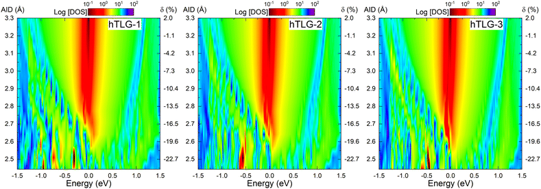 |
| | Fig. 2 Log-scale total density of states (DOS) as a function of energy and average interlayer distance (AID) or equivalently as an interlayer compression (δ). The Fermi level is set to 0 eV. | |
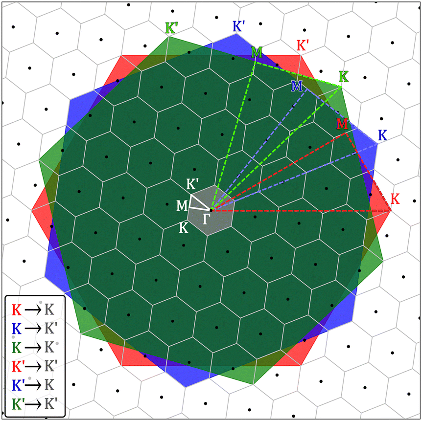
The band ‘folding’ is a common issue in electronic structure calculations for periodic systems with many primitive cells forming a commensurate supercell like hTLG. This band folding mechanism gives a ‘spaghetti’ of electronic states piled up into mini Brilluoin zone (BZ); and it frequently gives a difficult interpretation of physical interactions in a wide energy range when large supercells are studied. Standard supercell band structure calculations do not provide a direct comparison with angle-resolved photoemission spectroscopy (ARPES) measurements. Thus, an inverse approach to band folding can solve this problem to obtain an effective band structure showing physical interactions between layers and a more reliable comparison with experiments.24,26,48,49 To apply the unfolding mechanism described in ref. 49 we first plotted the BZs, the irreducible BZs, and the high symmetry points of three graphene primitive cells in the reciprocal space of the hTLG supercell in Fig. 3. With this representation of reciprocal space, we can now determine the correspondence of high-symmetry points (K and K′) from primitive cells with those in the hTLG supercell (see inset in Fig. 3). Note that even when K′ of the green layer, K of the blue layer, and K′ of the red layer are positioned in the K′ of the hTLG supercell, the electronic states of the green and red layers do not interact directly. Instead they interact through the blue layer. Therefore, we applied the unfolding approach along the dashed blue k-path connecting Γ → K → M → Γ points to calculate the spectral weight W(k, I) for each eigenstate, k is the wavevector and I is the band index, which is solved for each layer. Further details regarding the unfolding approach can be found in ref. 24, 26, 48 and 49.
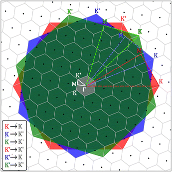 |
| | Fig. 3 Reciprocal space of periodic hTLG with θ = 21.78°. Lattice points represented with black dots are surrounded by gray hexagonal mini BZs. In the same supercell reciprocal space, the first BZs of graphene primitive cells and their corresponding irreducible BZs are plotted with green, blue and red colors. High symmetry points for the mini BZ are colored with light gray. | |
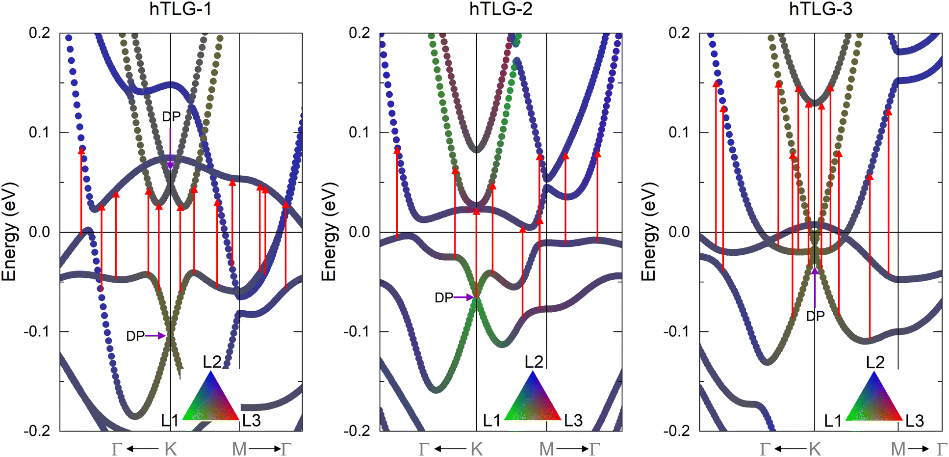
We chose the hTLG systems with AID = 3.03 Å (δ ∼ −6.37%) to apply the unfolding method because these systems do not show large differences in the total DOS in Fig. 2. The results in Fig. 4 show that the electronic states around the Fermi energy are due to the blue layer, which resembles the linear dispersion of Dirac cones. For energies lower than −1 eV, several discontinuities in the band structure were observed along the K–M path, where the electronic bands originated mainly from the outer green and red graphene layers. Three electronic bands were found for the K → Γ and M → Γ paths, from which the darker green band represents hybridization between the outer red (50%) and green (50%) layers. The outer bands near the Γ point (dark blue) have contributions from the red (25%), blue (50%), and green (25%) layers. We have identified less-dispersive electronic states just at the M point and −1 eV with gray color, which means an equal proportion (∼33.33%) of the three graphene layers. These last electronic states deserve further study because of the delocalization occurring along the direction perpendicular to the layers, whereas a high in-plane confinement is observed by the localized states.24 This could guide experimentalists to pursue the synthesis and in-depth characterization of three-dimensional (3D) twistronics in quantum layered materials.55
 |
| | Fig. 4 Unfolded band structures calculated along the high symmetry k-path for blue primitive cell. Along the same k-path, the electronic contributions from green and red layers are plotted. The normalized spectral weight, W(k, I), for the red, blue, and green layers are rescaled to integer values (from 0 to 255), to obtain a triad value for plotting each electronic state with circle symbols, whose size and color (in RGB format) are proportional to the W(k, I). The Fermi energy is set to 0 eV. The color triangle is defined to represent the L1, L2 and L3 layer contribution similar to Fig. 1. | |
3.3. Optical conductivity and absorbance
Because the hTLG systems were simulated as slabs of stacked graphene layers and a vacuum space within the supercell method, the macroscopic dielectric function, ε3D(ω), of the hTLG material can not be defined. Hence, to avoid the thickness problem, the 2D in-plane optical conductivity, σ2D(ω), is used instead of ε3D(ω)56 for linear optical property calculations. Note that the constraint of normal incidence of polarized light on the sample is considered. The relationship between ε3D(ω) and σ3D(ω) is as follows:| |
 | (6) |
where ε3D is ε in the bulk, ε0 is the vacuum permittivity and σ3D is the 3D bulk optical conductivity. Alternatively, σ3D(ω) = i[1 − ε3D(ω)]ε0ω. The σ3D(ω) can be related to the σ2D(ω) through the slab thickness L, as follows:57,58
Finally, the real part of σ2D (also known as the longitudinal conductivity component), Re[σ2D(ω)], was calculated instead of ε(ω),59,60 which is equivalent to the imaginary part of ε3D, Im[ε3D], and incorporates the light absorption mechanism in 2D materials. The Im[σ2D(ω)] term is similar to the Re[ε3D(ω)] term and is related to the refractive index. Thus, once the ground state electronic properties of the hTLG systems were calculated for several δ values, we proceeded to calculate the real, ε1(ω), and imaginary, ε2(ω), parts of the frequency-dependent complex dielectric function ε(ω). For this purpose, an electric field was applied along the x-direction to determine ε1(ω) and ε2(ω) within the single-particle approximation neglecting the Drude contributions (intraband transitions) for low energies. Thus, only the direct (q → 0) electronic interband transitions were calculated.
Fig. 5 shows the Re[σ2D] values for the three different hTLG systems as a function of δ. The uncompressed systems exhibited a sharp peak in ħω ∼ 4.2 eV due to transitions between electronic states located at the van Hove singularities (around the M point in the band structure) of graphene monolayer, meanwhile Re[σ2D] ≈ 3σ0 (with σ0 = e2π/2h the conductance quantum) at low energies. For most incident photon energies, a significant enhancement in Re[σ2D] is observed when the interlayer compression, δ, increases. However, a contrary effect is observed around ħω ∼ 4.2 eV, because Re[σ2D] dropped with the interlayer compression strength. Notice that, a peak splitting is observed with reduced intensities for the minimal compression strength (see the more intense blue lines), for ħω ∼ 4.2 eV. At low photon energies, the compressed trilayers exhibit the most remarkable increase in Re[σ2D]; see the bottom panels in Fig. 5. For a high compression value of δ ≈ −21.6%, the Re[σ2D] increased by up to ∼ 9.5σ0 (ħω = 90 meV), 18σ0 (ħω = 65 meV), and 10σ0 (ħω = 170 meV) for the hTLG-1, hTLG-2, and hTLG-3 systems, respectively. Furthermore, for the low-photon energy regime and intermediate compression values, the hTLG-1 system exhibited smaller values of Re[σ2D] than σ0, as shown in Fig. 5. The high Re[σ2D] values at low incident photon energies can be ascribed to direct electron transitions in the corresponding SC band structure, as shown in Fig. 6. The colored band structures in Fig. 6 show the contribution or mixing of each layer for every electronic state, in a format similar to that in Fig. 4. The possible direct band-to-band electronic transitions are indicated by the vertical red arrows, leading to the maximum conductivity values indicated by the small blue arrows in Fig. 5. Even when there are a large number of vertical electronic transitions, as shown in Fig. 6, the optical transition rate probability, which is a function of the average dipole moment operator, should be considered to discard electronic transitions with a null transition probability. It is important to note that the hTLG-2 structure with lower P symmetry has a maximum Re[σ2D] = 18σ0 value at a high δ compression.
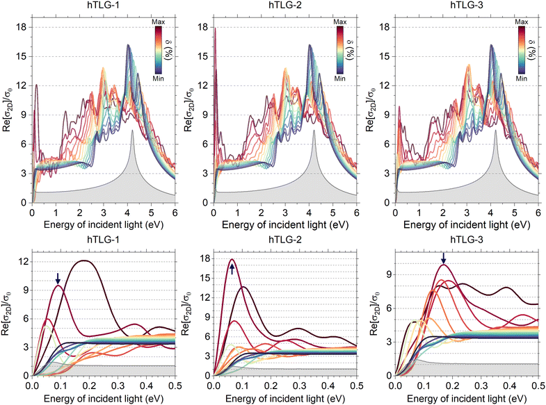 |
| | Fig. 5 Top panels: Real part of in-plane longitudinal optical conductivity, Re[σ2D], calculated for several δ values in a wide energy range of incident light. Bottom panels: The same as the top panels but for a lower incident photon energy. Blue arrows point to high peaks in Re[σ2D] when δ = −21.6%, for comparison purposes. To compare between results, the Re[σ2D] of the graphene monolayer is plotted with gray color. σ0 = e2π/2h. | |
 |
| | Fig. 6 Supercell electronic band structures calculated along the paths defined by the high symmetry points in Fig. 3. The high compression value is δ = −21.6%. Different layer contributions in the band structure are plotted with green (layer 1), blue (layer 2) and red (layer 3). Dirac points (DP) observed below zero eV means an n-doping effect. Vertical dashed red arrows indicate possible direct electron transitions. The Fermi energy is set to 0 eV. | |
The enhancement of Re[σ2D] for energies less than 0.5 eV, and in the energy range between ∼1.5 to ∼3.5 eV, is a clear fingerprint of an increase in optical absorbance, A, for the incident perpendicular light to the system because:61
| |
 | (8) |
where
c is the speed of light. On the other hand, we also calculated the in-plane linear optical absorption coefficient,
α(
ω), from the
ε1(
ω) and the
ε2(
ω) parts as follows:
| |
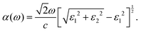 | (9) |
Fig. 7 shows the calculated α values for the different δ values. The rainbow window indicates the photon energy in the visible range. Generally, an α enhancement is observed as the interlayer compression increases. However, around ħω ∼ 4.2 eV, the compression strength suppresses the optical absorption as was observed for Re[σ2D], according with the experimental results of pressurized trilayer graphene.62 Theoretical studies have reported that, for non-twisted multilayer graphene with Bernal stacking (ABAB…), the peak intensity in α increases as the number of graphitic layers do, and peak splitting at ħω ∼ 4.2 eV emerges for trilayer and tetra-layered systems using out-of-plane polarization components of the electromagnetic field.63 These results show that for low incident energies, <0.5 eV, the hTLG systems absorb perpendicular or parallel incident electromagnetic radiation differently, with more prominent perpendicular absorbance properties for the hTLG-2 structure, as shown in Fig. 5.
 |
| | Fig. 7 In-plane linear optical absorption as a function of incident energy light and interlayer compression δ. The rainbow window delimit the energy range of visible electromagnetic spectrum. | |
4. Conclusions
We studied the structural, electronic, and linear optical properties of three different periodic helical three-layer graphene (hTLG) systems using the total-energy DFT formalism. The interplay between the initial stacking (sub-lattice exchange parity) and interlayer distance for the tuning and enhancement of electronics and optics was addressed. Once the periodic atomic models were built, the diffraction patterns were calculated by considering the structure factor to detect the differences among the three configurations. Loss-symmetry behavior was observed from the highest (hTLG-1) to the lowest (hTLG-2) structure. Regarding the electronic structure, the total density of states is a tunable electronic property because it depends on the initial stacking fault and interlayer compression to achieve strongly localized asymmetric states around the Fermi level. The calculated effective band structures reveal clear interlayer interactions, such as hybridizations, and are likely in-plane confined but normal plane delocalized electronic states that connect the three layers. Finally, a substantial enhancement is observed in the linear optical properties, such as in the optical conductivity for lower energies (<1.5 eV) and in the optical absorbance mainly in the visible spectrum for practical optoelectronic applications. These theoretical results demonstrate the importance of initial vertical stacking and interlayer compression in the electronics and optics of hTLG superlattices, which can conveniently lead to experimentalists.
Author contributions
Ossiel Aguilar contributed to the investigation, software, resources, and validation of data. Alberto Rubio and Florentino López contributed to the conceptualization, formal analysis, investigation, supervision, validation, and visualization. Francisco Sánchez contributed to the conceptualization, formal analysis, supervision, investigation, and writing and editing of the original draft.
Data availability
Data will be made available from the corresponding author upon reasonable request.
Conflicts of interest
There are no conflicts to declare.
Acknowledgements
Francisco Sánchez-Ochoa acknowledges the financial support from SECIHTI (CONAHCYT) Grant No. CF-2023-I-336 and DGAPA-UNAM Grant No. PAPIIT IA105623. Numerical calculations were performed in the Holiday cluster at the Physics Institute (UNAM). The authors thank Carlos Ernesto Lopez Nataren for technical assistance.
References
- Y. Cao, V. Fatemi, S. Fang, K. Watanabe, T. Taniguchi, E. Kaxiras and P. Jarillo-Herrero, Nature, 2018, 556, 43–50 CrossRef CAS PubMed.
- M. Yankowitz, S. Chen, H. Polshyn, Y. Zhang, K. Watanabe, T. Taniguchi, D. Graf, A. F. Young and C. R. Dean, Science, 2019, 363, 1059–1064 CrossRef CAS PubMed.
- X. Lu, P. Stepanov, W. Yang, M. Xie, M. A. Aamir, I. Das, C. Urgell, K. Watanabe, T. Taniguchi and G. Zhang, et al., Nature, 2019, 574, 653–657 CrossRef CAS PubMed.
- P. Stepanov, I. Das, X. Lu, A. Fahimniya, K. Watanabe, T. Taniguchi, F. H. Koppens, J. Lischner, L. Levitov and D. K. Efetov, Nature, 2020, 583, 375–378 CrossRef CAS PubMed.
- M. Oh, K. P. Nuckolls, D. Wong, R. L. Lee, X. Liu, K. Watanabe, T. Taniguchi and A. Yazdani, Nature, 2021, 600, 240–245 CrossRef CAS PubMed.
- F. López-Urías, A. Rubio-Ponce, E. Muñoz-Sandoval and F. Sánchez-Ochoa, J. Phys.: Condens. Matter, 2024, 36, 405802 CrossRef PubMed.
- F. López-Urías, A. Rubio-Ponce, E. Muñoz-Sandoval and F. Sánchez-Ochoa, Phys. Chem. Chem. Phys., 2024, 26, 16955–16962 RSC.
- J. M. B. Lopes dos Santos, N. M. R. Peres and A. H. Castro Neto, Phys. Rev. Lett., 2007, 99, 256802 CrossRef CAS PubMed.
- E. Suárez Morell, J. D. Correa, P. Vargas, M. Pacheco and Z. Barticevic, Phys. Rev. B, 2010, 82, 121407 CrossRef.
- G. Trambly de Laissardiere, D. Mayou and L. Magaud, Nano Lett., 2010, 10, 804–808 CrossRef CAS PubMed.
- R. Bistritzer and A. H. MacDonald, Proc. Natl. Acad. Sci. U. S. A., 2011, 108, 12233–12237 CrossRef CAS PubMed.
- J. M. Park, Y. Cao, K. Watanabe, T. Taniguchi and P. Jarillo-Herrero, Nature, 2021, 590, 249–255 CrossRef CAS PubMed.
- Z. Hao, A. Zimmerman, P. Ledwith, E. Khalaf, D. H. Najafabadi, K. Watanabe, T. Taniguchi, A. Vishwanath and P. Kim, Science, 2021, 371, 1133–1138 CrossRef CAS PubMed.
- H. Kim, Y. Choi, C. Lewandowski, A. Thomson, Y. Zhang, R. Polski, K. Watanabe, T. Taniguchi, J. Alicea and S. Nadj-Perge, Nature, 2022, 606, 494–500 CrossRef CAS PubMed.
- X. Liu, N. J. Zhang, K. Watanabe, T. Taniguchi and J. Li, Nat. Phys., 2022, 18, 522–527 Search PubMed.
- J. M. Park, Y. Cao, L.-Q. Xia, S. Sun, K. Watanabe, T. Taniguchi and P. Jarillo-Herrero, Nat. Mater., 2022, 21, 877–883 CrossRef CAS PubMed.
- Y. Zhang, R. Polski, C. Lewandowski, A. Thomson, Y. Peng, Y. Choi, H. Kim, K. Watanabe, T. Taniguchi and J. Alicea, et al., Science, 2022, 377, 1538–1543 CrossRef CAS PubMed.
- E. Y. Andrei and A. H. MacDonald, Nat. Mater., 2020, 19, 1265–1275 CrossRef CAS PubMed.
- L. Balents, C. R. Dean, D. K. Efetov and A. F. Young, Nat. Phys., 2020, 16, 725–733 Search PubMed.
- C. Yang, J. May-Mann, Z. Zhu and T. Devakul, Phys. Rev. B, 2024, 110, 115434 CrossRef CAS.
- T. Devakul, P. J. Ledwith, L.-Q. Xia, A. Uri, S. C. de la Barrera, P. Jarillo-Herrero and L. Fu, Sci. Adv., 2023, 9, eadi6063 CrossRef CAS PubMed.
- X. Zhang, K.-T. Tsai, Z. Zhu, W. Ren, Y. Luo, S. Carr, M. Luskin, E. Kaxiras and K. Wang, Phys. Rev. Lett., 2021, 127, 166802 CrossRef CAS PubMed.
- P. Moon, Phys. Rev. B, 2021, 104, 115407 CrossRef CAS.
- F. Sánchez-Ochoa, A. R. Botello-Méndez and C. Noguez, Phys. Rev. B, 2021, 104, 075430 CrossRef.
- S. Carr, S. Fang, P. Jarillo-Herrero and E. Kaxiras, Phys. Rev. B, 2018, 98, 085144 CrossRef CAS.
- F. Sánchez-Ochoa, A. Rubio-Ponce and F. López-Urías, Phys. Rev. B, 2023, 107, 045414 CrossRef.
- F. Munoz, H. P. O. Collado, G. Usaj, J. O. Sofo and C. A. Balseiro, Phys. Rev. B, 2016, 93, 235443 CrossRef.
- H. Shi, Z. Zhan, Z. Qi, K. Huang, E. V. Veen, J. Á. Silva-Guillén, R. Zhang, P. Li, K. Xie and H. Ji, et al., Nat. Commun., 2020, 11, 1–7 CrossRef PubMed.
- X. Lin, H. Zhu and J. Ni, Phys. Rev. B, 2020, 101, 155405 CrossRef CAS.
- T. Zhang, C. Gao, D. Liu, Z. Li, H. Zhang, M. Zhu, Z. Zhang, P. Zhao, Y. Cheng and W. Huang, Nano Lett., 2022, 22, 5841–5848 CrossRef CAS PubMed.
- W. Xiong, L. Wen, X. Lv and Z. Li, Phys. Lett. A, 2023, 483, 129048 CrossRef CAS.
- V. G. M. Duarte, D. R. da Costa, N. M. R. Peres, L. K. Teles and A. J. Chaves, Phys. Rev. B, 2024, 110, 035405 CrossRef CAS.
- Y. Hou, J. Zhou, M. Xue, M. Yu, Y. Han, Z. Zhang and Y. Lu, Small, 2024, 2311185 CrossRef PubMed.
- N. P. Kazmierczak, M. Van Winkle, C. Ophus, K. C. Bustillo, S. Carr, H. G. Brown, J. Ciston, T. Taniguchi, K. Watanabe and D. K. Bediako, Nat. Mater., 2021, 20, 956–963 CrossRef CAS PubMed.
- L. Ge, K. Ni, X. Wu, Z. Fu, Y. Lu and Y. Zhu, Nanoscale, 2021, 13, 9264–9269 RSC.
- A. H. Castro Neto, F. Guinea, N. M. R. Peres, K. S. Novoselov and A. K. Geim, Rev. Mod. Phys., 2009, 81, 109–162 CrossRef CAS.
- E. J. Mele, J. Phys. D: Appl. Phys., 2012, 45, 154004 CrossRef.
- E. J. Mele, Phys. Rev. B: Condens. Matter Mater. Phys., 2010, 81, 161405 CrossRef.
- S. Talkington and E. J. Mele, Phys. Rev. B, 2023, 108, 085421 CrossRef CAS.
- S. Talkington and E. J. Mele, Phys. Rev. B, 2023, 107, L041408 CrossRef CAS.
- P. Ordejón, E. Artacho and J. M. Soler, Phys. Rev. B: Condens. Matter Mater. Phys., 1996, 53, R10441 CrossRef PubMed.
- J. M. Soler, E. Artacho, J. D. Gale, A. Garca, J. Junquera, P. Ordejón and D. Sánchez-Portal, J. Phys.: Condens. Matter, 2002, 14, 2745 CrossRef CAS.
- J. P. Perdew, K. Burke and M. Ernzerhof, Phys. Rev. Lett., 1996, 77, 3865–3868 CrossRef CAS PubMed.
- N. Troullier and J. L. Martins, Phys. Rev. B: Condens. Matter Mater. Phys., 1991, 43, 1993 CrossRef CAS PubMed.
- H. J. Monkhorst and J. D. Pack, Phys. Rev. B: Solid State, 1976, 13, 5188–5192 CrossRef.
- K. Momma and F. Izumi, J. Appl. Crystallogr., 2011, 44, 1272–1276 CrossRef CAS.
- O. Aguilar-Espíndola, OssielAg/Nook-iin: Nook'iin: First public version, 2024 DOI:10.5281/zenodo.14257397.
- F. Hidalgo, F. Sánchez-Ochoa and C. Noguez, npj 2D Mater. Appl., 2023, 7, 40 CrossRef CAS.
- F. Sánchez-Ochoa, F. Hidalgo, M. Pruneda and C. Noguez, J. Phys.: Condens. Matter, 2020, 32, 025501 CrossRef PubMed.
- P. J. Brown, A. G. Fox, E. N. Maslen, M. A. O'Keefe and B. T. M. Willis, in International Tables for Crystallography Volume C: Mathematical, physical and chemical tables, ed. E. Prince, Springer, Netherlands, 2004, vol. C, pp. 554–595 Search PubMed.
- A. Togo, K. Shinohara and I. Tanaka, arXiv, preprint, 2018, arXiv:1808.01590 Search PubMed.
- F. Yndurain, Phys. Rev. B, 2019, 99, 045423 CrossRef.
- M. Yankowitz, J. Jung, E. Laksono, N. Leconte, B. L. Chittari, K. Watanabe, T. Taniguchi, S. Adam, D. Graf and C. R. Dean, Nature, 2018, 557, 404–408 CrossRef CAS PubMed.
- J. Klimeš, D. R. Bowler and A. Michaelides, J. Phys.: Condens. Matter, 2009, 22, 022201 CrossRef PubMed.
- F. Wu, R.-X. Zhang and S. Das Sarma, Phys. Rev. Res., 2020, 2, 022010 CrossRef CAS.
- T. Zhan, X. Shi, Y. Dai, X. Liu and J. Zi, J. Phys.: Condens. Matter, 2013, 25, 215301 CrossRef PubMed.
- L. Matthes, O. Pulci and F. Bechstedt, New J. Phys., 2014, 16, 105007 CrossRef.
- L. Matthes, O. Pulci and F. Bechstedt, Phys. Rev. B, 2016, 94, 205408 CrossRef.
- A. Gusso, F. Sánchez-Ochoa and R. Esquivel-Sirvent, Langmuir, 2024, 40, 10685–10694 CrossRef CAS PubMed.
- R. Esquivel-Sirvent, A. Gusso and F. Sánchez Ochoa, Nanoscale Microscale Thermophys. Eng., 2023, 27, 95–109 Search PubMed.
- K. F. Mak, L. Ju, F. Wang and T. F. Heinz, Solid State Commun., 2012, 152, 1341–1349 CrossRef CAS.
- F. Ke, Y. Chen, K. Yin, J. Yan, H. Zhang, Z. Liu, J. S. Tse, J. Wu, H.-K. Mao and B. Chen, Proc. Natl. Acad. Sci. U. S. A., 2019, 116, 9186–9190 CrossRef CAS PubMed.
- A. Kumar, G. Sachdeva, R. Pandey and S. P. Karna, Appl. Phys. Lett., 2020, 116, 263102 CrossRef CAS.
Footnote |
| † Electronic supplementary information (ESI) available: Atomic models of primitive cells and twisted bilayer systems with different initial stacking, general information on the number of carbon atoms and interlayer angles in helical systems, comparison between two helical systems with different angles, and electronic band structures with different approximations. See DOI: https://doi.org/10.1039/d5cp00337g |
|
| This journal is © the Owner Societies 2025 |
Click here to see how this site uses Cookies. View our privacy policy here. 
 Open Access Article
 This Open Access Article is licensed under a
  a,
Alberto Rubio-Ponce
a,
Alberto Rubio-Ponce


 . Additionally, the |det