
 Open Access Article
 This Open Access Article is licensed under a
 Creative Commons Attribution 3.0 Unported Licence
Structure and stability of copper nanoclusters on monolayer tungsten dichalcogenides†
Michael Sweetman ,
Cara-Lena Nies and
Michael Nolan*
,
Cara-Lena Nies and
Michael Nolan*
Tyndall National Institute, University College Cork, Lee Maltings, Dyke Parade, Cork, T12 R5CP, Ireland. E-mail: michael.nolan@tyndall.ie
First published on 28th January 2025
Abstract
Layered materials, such as tungsten dichalcogenides (TMDs), are being studied for a wide range of applications, due to their unique and varied properties. Specifically, their use as either a support for low dimensional catalysts or as an ultrathin diffusion barrier in semiconductor devices interconnect structures are particularly relevant. In order to fully realise these possible applications for TMDs, understanding the interaction between metals and the monolayer they are deposited on is of utmost importance. The morphology that arises due to given metal–substrate combinations determines their possible applications and thus is a central characteristic. Previous theoretical studies typically focus on the effects which single metal adatoms, or dopants, have on a TMDs’ electronic and optical properties, thereby leaving a knowledge gap in terms of thin film nucleation on TMD monolayers. To address this, we present a density functional theory (DFT) study of the adsorption of small Cu clusters on a range of TMD monolayers, namely WS2, WSe2, and WTe2. We explore how metal–substrate and metal–metal interactions contribute to both the stability of these Cu clusters and their morphology, and investigate the role of the chalcogen in these interactions. We find that single Cu atoms adsorb most strongly to the adsorption site above the W atom, however as nanocluster size increases, Cu tends to be adsorbed atop the chalcogen atoms in the monolayer to facilitate Cu–Cu bond formation. We show that Cu–Cu interactions drive the stability of the adsorbed Cu nanoclusters, with a clear preference for 3D structures on all 3 monolayers studied. Furthermore, significant Cu migration occurs during 0 K relaxation. This, combined with the small activation barriers found for Cu migration suggest facile and dynamic cluster behaviour at finite temperature on all three monolayers. Finally, we find that Cu clusters are generally most stable on WTe2 and least stable on WSe2. This difference however is typically only in the range of 0.1 eV.
1 Introduction
2D materials have become increasingly relevant in a wide variety of research areas, ever since the initial exfoliation of graphene in 2004.1 Since graphene's discovery, many classes of 2D materials have been discovered, such as hexagonal-boron nitride, MXenes and transition metal dichalcogenides (TMDs); each with their own unique and distinct properties, and applications.2–6TMDs are a class of layered materials in which, similarly to graphite, there are covalently bonded monolayers with van der Waals interactions between layers to form layered bulk structures. Unlike graphite, where all atoms are in a single plane, TMD monolayers consist of a covalent X–M–X “sandwich structure”, with X and M being the chalcogen and metal species respectively.7 These materials have a wide range of optical,8–11 electrical,12,13 and mechanical properties.14–16
Properties of monolayer TMDs tend to differ from those of their layered bulk structures.17,18 For example, bulk WS2 has an indirect bandgap, whereas monolayer WS2 has a direct bandgap.19 Furthermore, the properties of TMD monolayers can differ dramatically depending on both the metal, chalcogenide, crystal phase, and stacking pattern that is present.20 For example, 1T-TiS2 is metallic whereas 1T-TiSe2 is a semi-metal.21,22 This breadth of material properties leads to a diversity of possible applications.
Tungsten TMDs (WS2, WSe2, WTe2; henceforth collectively denoted as WX2) are important for applications in catalysis,23–25 optoelectronics,26,27 spintronics,28,29 gas sensors,30–32 antibacterial activity,33,34 etc. Moreover, there are a wide range of methods available to synthesise these materials such as chemical vapour deposition,35–37 atomic layer deposition,38,39 and exfoliation.40 This makes tungsten TMDs useful as engineering materials, rather than just as simple model systems.
Many technologies, including energy conversion and electronics, are dependent on metals deposited onto substrates. The resulting morphology of the metal on the substrate determines the possible application of metal–substrate combinations.41 For example, metals which wet a surface and can be deposited in a flat, non-island morphology, are needed as conducting metals for interconnects in semiconductor devices.42 This is particularly relevant as TMDs have shown promise as diffusion barriers for Cu in CMOS interconnect structures, allowing for atomically thin barriers which can maximise the volume of the interconnect metal in vias. This is important for next generation technology nodes such as Gate-All-Around and Complementary Field Effect Transistors, as it would keep line resistance low while allowing downscaling of CMOS structures.43–47 Furthermore, metals which do not wet the surface, but rather form 3D clusters when deposited, have applications in catalysis due to their large surface to volume ratio, providing a large number of active sites.48 While TMDs have shown promise for the hydrogen evolution reaction,49 the basal plane of the monolayer remains practically inert.50 Augmenting TMD monolayers with metal nanoparticles may provide a path to increase the capabilities of TMDs as catalysts.51,52 Therefore, strategies are needed to predict morphology of deposited metals on TMDs which can enable next generation interconnects or active catalysts for energy conversion chemistry.
Current literature concerning modification of tungsten TMD monolayers with metals typically investigates the effect of either doping, or adsorption of metals. Studies concerning monolayer doping, generally where metal atoms substitute a chalcogen atom in the monolayer, investigate the dopant's effects on electronic and magnetic properties (Mn, Fe, Co, and Ni doped WS2),53–55 optical properties (V on WSe2),56 and gas sensing (Cu, Co, Rh, Ir doped WS2 and Ni doped WTe2).57–59 There are also studies concerning doping at the metal rather than the chalcogen site in TMD monolayers (Re, Au, or W doping MoS2),60,61 however these studies are less widespread.
Similarly, studies concerning metal adsorption are largely focused on the effect of single atom adsorption, and investigating its influence on various properties such as electronic properties (Cr, Mn, Fe, Co, Ni, Cu, etc. on WS2, Pd on WSe2),62–65 spintronics (3d transition metals on WS2),66 and gas sensing (Pd, Ag, Au, Pt on WSe2, Na, Li, Pd on WTe2).67–70
As current literature concerning metal adsorption onto tungsten TMD monolayers largely investigates the effects of single metal atom adsorption, it is clear that there does not exist a comprehensive insight into the behaviour of metals at the early stages of nucleation or a prediction of overall morphology of metals on the TMD monolayers of WS2, WSe2, and hexagonal WTe2. It is also important to understand any role played by the TMD in controlling the metal morphology which is lacking to date.
Building on work in ref. 71 and 72, this study provides an atomistic description of copper nanocluster (Cun, n = 1–4) adsorption onto three different tungsten dichalcogenide monolayers. Descriptors such as the copper–surface and copper–copper interaction energies provide an understanding of the nanocluster adsorption structure, and can be used to predict the final morphology of copper thin films on these surfaces. For example, our previous work on the morphology of Cu clusters on MoS2![[thin space (1/6-em)]](https://www.rsc.org/images/entities/char_2009.gif) 71 and TaN73 shows that if the copper–surface interaction is larger than the copper–copper interaction, then 2D growth of the metal can be expected, with 3D growth expected if the copper–copper interaction energy is larger than the copper–surface interaction energy.74 Furthermore, if the metal adsorption energy is larger than the cohesive energy of the corresponding bulk metal, than 2D growth is expected.75
71 and TaN73 shows that if the copper–surface interaction is larger than the copper–copper interaction, then 2D growth of the metal can be expected, with 3D growth expected if the copper–copper interaction energy is larger than the copper–surface interaction energy.74 Furthermore, if the metal adsorption energy is larger than the cohesive energy of the corresponding bulk metal, than 2D growth is expected.75
Moreover, if the metal–metal interaction energy is larger than the metal–surface interaction energy, increasing temperature for this metal–substrate combination would tend to promote 3D growth and island morphology. However, increasing temperature for combinations where the deposited metal has a larger metal–surface interaction energy, would promote 2D growth of the metal.
By comparing adsorption across three different WX2 monolayers in the same hexagonal structure, the effect of the chalcogen atom on the stability of copper clusters and the resulting morphology (2D or 3D) can be investigated. The results of this work show that the stability of copper clusters on WX2 monolayers is mainly driven by the copper–copper interaction, with a clear preference for 3D morphology. Furthermore, the chalcogen species present in the WX2 monolayer has a negligible effect on adsorption energies, particularly as cluster size increases. The key factor for Cu morphology is its weaker copper–surface energy, compared to its copper–copper interaction energy.
2 Computational methods
All calculations were performed with density functional theory (DFT) using the Vienna Ab initio Simulation Package (VASP) version 5.4.4.76 Periodic three-dimensional boundary conditions were applied, and the spin-polarized general gradient approximation (GGA) using the Perdew–Burke–Ernzerhof (PBE) approximation to the exchange–correlation functional were used to describe the system.77The valence electrons were described explicitly using a plane-wave basis set with an energy cut-off of 450 eV. The valence electron configurations used for the chemical species are: W = 6s1 5d5; Cu = 4s1 3d10; S = 3s2 3p4; Se = 4s2 4p4; Te = 5s2 5p4. The core electrons were described using the projector-augmented wave potential (PAW).76,78 A Monkhorst–Pack k-point grid of 2 × 2 × 1 was used. All forces acting on the atoms were converged to within 0.02 eV Å−1, with convergence criteria for energy minimisation set to the default value of 10−4 for geometry relaxations. A Methfessel–Paxton smearing of order 1 was used and no symmetry was applied. We use a Gaussian smearing of σ = 0.1 eV. A vacuum greater than 17 Å was applied to separate the repeating images for the monolayer along the z direction.
Activation energies for atomic transitions were calculated using the climbing image nudged elastic band method (CI-NEB) with 5 images, including starting and ending structures. The convergence criteria in the CI-NEB are 0.02 eV Å−1.
Vibrational analysis and ab initio molecular dynamics were used to determine the stability of single atom adsorption at an adsorption site (vide infra). Vibrational analysis was performed by computing second-order force constants using finite differences, with no symmetry imposed. The convergence criteria for energy minimisation was set to 10−7 eV to ensure accuracy. Only sulphur atoms directly below the adsorbed Cu atom, the three nearest W atoms to the Cu, and the Cu atom itself were not frozen in this analysis. The molecular dynamics simulations were performed in the NVT ensemble with an energy cutoff of 250 eV, and temperature of 100 K. A timestep of 2.5 fs for 2000 steps was used resulting in an overall simulation time of 5 ps.
Similar to previous work69,72 we use a 5 × 5 × 1 supercell of WX2, where X is either S, Se, or Te, with 75 atoms in the supercell. These WX2 monolayers have the same hexagonal structure as MoS2 monolayers, only differing by lattice parameter and the metal–chalcogenide bond length.
For each monolayer α = β = 90°, γ = 120°. For WS2, WSe2, and WTe2 respectively: a = b = 15.91 Å, c = 21.02 Å; a = b = 16.58 Å, c = 21.40 Å; and a = b = 17.76 Å, c = 23.46 Å. The optimised geometries have W–chalcogenide bond lengths of 2.42 Å, 2.55 Å, and 2.74 Å for the sulphide, selenide, and telluride respectively. These values agree well with previous theoretical values for the tungsten chalcogenide bond length in these structures.79–81
van der Waals (vdW) corrections were not used in this study as we have previously shown that vdW interactions do not contribute significantly to the stability and optimised geometry of metal clusters on TMD monolayers.72 Structures were visualised using the atomic simulation environment (ASE) and VESTA.82,83
The majority of TMDs have a stable 2H phase at room temperature, WTe2 however, only has a metastable 2H phase, with its orthorhombic 1T and 1T′ being the more stable phases at ambient conditions.84,85 Despite this, we are only investigating WTe2 in its metastable 2H phase. Hexagonal WTe2 has unique properties compared to its orthorhombic phase which makes it particularly interesting in its use as a channel material for tunnel field-effect transistors.86 There is research on the interactions of these WTe2 monolayers with bulk metals.87 However, this does not provide insight into the early stages of metal nucleation, but only describes whether such an interface is energetically stable. Furthermore, there is some initial work on the use of WTe2 as a gas sensor in its hexagonal phase,58,70,88 however this focuses only on doping of the monolayer and thus the behaviour of adsorbed metal clusters on 2H WTe2 is still unknown. Moreover, by studying WTe2 in its 2H phase, direct comparisons between metal adsorption on all three surfaces of the same phase can be made, due to the equivalent crystal structures.
To understand Cu adsorption, and predict the likely nucleation mechanism of Cu on each WX2 monolayer, we compute three different types of energy according to previous work72–74
1. The binding energy per copper atom:
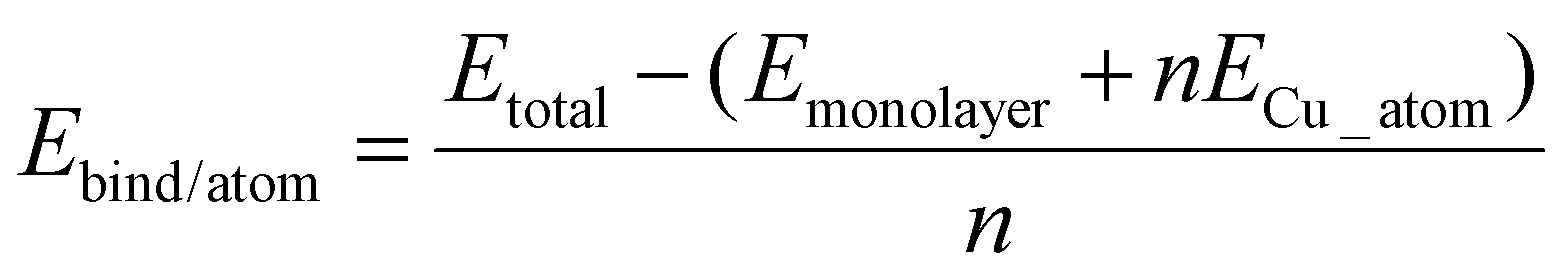 | (1) |
2. The interaction energy between adsorbed copper atoms, referred to as the metal–metal interaction energy:
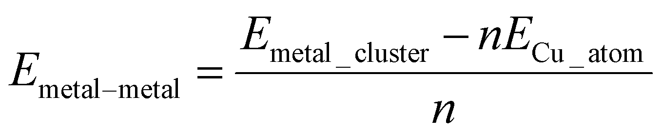 | (2) |
3. The binding energy with reference to free Cun cluster (Emetal_cluster, see eqn (2)), also referred to as the copper–substrate interaction energy:
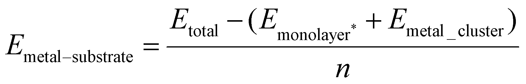 | (3) |
Here Emonolayer* is the single point energy of the monolayer with no Cu, in its relaxed structure. We use this energy, rather than the monolayer energy used in eqn (1), as the adsorption of atoms introduces a local strain and distortion to the monolayer. Due to this local strain caused by the adsorbed species, the total energy of the monolayer will be altered from that of the bare monolayer.
From these equations it is possible to disaggregate the overall binding energy per atom into its components, namely metal–surface interactions, metal–metal interaction, and a surface distortion term.
| Ebind/atom = Emetal–surface + Emetal–metal + Edistortion | (4) |
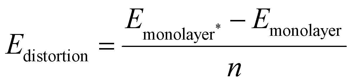 | (5) |
3 Results and discussion
To investigate the early stages of Cu nucleation on these TMD monolayers, Cun (n = 1–4) nanoclusters are adsorbed onto the TMD monolayers on different sites and in different morphologies. Binding energies for each structure are calculated using eqn (1) and shown in Tables 1 and 2. Metal–substrate interaction energies are calculated using eqn (3) and shown in Table 3. Furthermore, metal–metal interactions energies are calculated using eqn (2) and shown in Table 4.| X | M | H | B | |
|---|---|---|---|---|
| WS2 | −0.68 | −1.03 | −0.91 | −0.85 |
| WSe2 | −0.59 | −0.94 | −0.86 | −0.78 |
| WTe2 | −0.66 | −1.13 | −1.09 | −0.95 |
| # Cu | XX | XM | MH | XH | X-sep | M-sep | H-sep | |
|---|---|---|---|---|---|---|---|---|
| 2 | WS2 | −1.50 | −1.49 | −1.03 | −1.48 | −0.67 | −1.03 | −0.96 |
| WSe2 | −1.46 | −1.47 | −0.92 | −1.46 | −0.59 | −0.94 | −0.89 | |
| WTe2 | −1.57 | −1.60 | −1.18 | −1.58 | −0.65 | −1.12 | −1.12 |
| Line-X | -M | -H | Offset-X | -M | -H | Triangle-X | -M | 3D-Triangle-X | -M | ||
|---|---|---|---|---|---|---|---|---|---|---|---|
| 3 | WS2 | −1.64 | −1.72 | −1.71 | −1.23 | −1.34 | — | −1.68 | −1.77 | −1.76 | −1.75 |
| WSe2 | −1.60 | −1.70 | −1.66 | −1.16 | −1.26 | −1.26 | −1.61 | −1.42 | −1.68 | −1.72 | |
| WTe2 | −1.69 | −1.72 | — | −1.24 | −1.38 | −1.41 | −1.70 | −1.70 | −1.74 | −1.77 |
| Wire-X | -M | -H | Rhombus-X | -M | 3D-Rectangle-X | -M | -H | Tetrahedron-X | -M | -H | ||
|---|---|---|---|---|---|---|---|---|---|---|---|---|
| Different starting structures can relax identical adsorption modes, albeit with slightly different energies. For these tables, the largest binding energy for each adsorption mode, and its corresponding metal–surface and metal–metal interaction energies, is shown. Note that configurations with no energy value given in these tables were used as starting structures, but have relaxed to a configuration already displayed, e.g. S-Offset-H relaxes to a structure identical to S-Triangle-M. | ||||||||||||
| 4 | WS2 | −1.51 | −1.89 | −1.69 | −1.93 | −1.94 | −1.95 | −1.78 | — | −1.87 | −1.72 | — |
| WSe2 | −1.45 | −1.83 | — | −1.88 | −1.90 | −1.90 | −1.74 | — | −1.80 | −1.69 | −1.70 | |
| WTe2 | −1.57 | −1.61 | −1.36 | −1.98 | −1.97 | −1.95 | −1.97 | −1.90 | −1.86 | −1.80 | — | |
| # Cu | XX | XM | MH | XH | X-sep | M-sep | H-sep | |
|---|---|---|---|---|---|---|---|---|
| 2 | WS2 | −0.37 | −0.42 | −1.41 | −0.35 | −0.67 | −1.09 | −1.01 |
| WSe2 | −0.34 | −0.39 | −0.96 | −0.34 | −0.60 | −1.00 | −0.94 | |
| WTe2 | −0.44 | −0.54 | −1.24 | −0.46 | −0.66 | −1.18 | −1.15 |
| Line-X | -M | -H | Offset-X | -M | -H | Triangle-X | -M | 3D-Triangle-X | -M | ||
|---|---|---|---|---|---|---|---|---|---|---|---|
| 3 | WS2 | −0.44 | −0.51 | −0.51 | −0.47 | −0.63 | — | −0.45 | −0.56 | −0.51 | −0.53 |
| WSe2 | −0.39 | −0.48 | −0.44 | −0.41 | −0.53 | −0.54 | −0.40 | −0.21 | −0.45 | −0.55 | |
| WTe2 | −0.52 | −0.57 | — | −0.49 | −0.65 | −0.66 | −0.48 | −0.50 | −0.52 | −0.56 |
| Wire-X | -M | -H | Rhombus-X | -M | 3D-Rectangle-X | -M | -H | Tetrahedron-X | -M | -H | ||
|---|---|---|---|---|---|---|---|---|---|---|---|---|
| 4 | WS2 | −0.36 | −0.39 | −0.39 | −0.34 | −0.38 | −0.35 | −0.51 | — | −0.51 | −0.41 | — |
| WSe2 | −0.31 | −0.34 | — | −0.29 | −0.34 | −0.31 | −0.48 | — | −0.44 | −0.37 | −0.35 | |
| WTe2 | −0.44 | −0.53 | −0.85 | −0.38 | −0.41 | −0.35 | −0.53 | −0.42 | −0.49 | −0.53 | — |
| # Cu | XX | XM | MH | XH | X-sep | M-sep | H-sep | |
|---|---|---|---|---|---|---|---|---|
| 2 | WS2 | −1.14 | −1.12 | −0.05 | −1.14 | 0.00 | 0.00 | 0.00 |
| WSe2 | −1.14 | −1.12 | −0.04 | −1.13 | 0.01 | 0.00 | 0.01 | |
| WTe2 | −1.14 | −1.13 | −0.04 | −1.14 | 0.00 | 0.00 | 0.00 |
| Line-X | -M | -H | Offset-X | -M | -H | Triangle-X | -M | 3D-Triangle-X | -M | ||
|---|---|---|---|---|---|---|---|---|---|---|---|
| 3 | WS2 | −1.24 | −1.24 | −1.23 | −0.77 | −0.76 | — | −1.24 | −1.24 | −1.25 | −1.25 |
| WSe2 | −1.24 | −1.24 | −1.24 | −0.76 | −0.76 | −0.74 | −1.24 | −1.23 | −1.24 | −1.24 | |
| WTe2 | −1.24 | −1.19 | — | −0.77 | −0.77 | −0.77 | −1.25 | −1.24 | −1.25 | −1.24 |
| Wire-X | -M | -H | Rhombus-X | -M | 3D-Rectangle-X | -M | -H | Tetrahedron-X | -M | -H | ||
|---|---|---|---|---|---|---|---|---|---|---|---|---|
| 4 | WS2 | −1.15 | −1.50 | −1.33 | −1.61 | −1.57 | −1.60 | −1.30 | — | −1.37 | −1.35 | — |
| WSe2 | −1.15 | −1.50 | — | −1.60 | −1.57 | −1.60 | −1.29 | — | −1.37 | −1.36 | −1.36 | |
| WTe2 | −1.14 | −1.13 | −0.53 | −1.61 | −1.58 | −1.61 | −1.49 | −1.49 | −1.37 | −1.36 | — |
As in previous work involving nanocluster adsorption onto TMD surfaces,71,72 three stable, non-equivalent adsorption sites exist on the TMD monolayer. Atop-X, where Cu adsorbs directly above the chalcogen; Atop-M, where Cu adsorbs above tungsten so that the adsorbed atom is coordinated to three chalcogens; and Hollow, where the adatom is coordinated to three chalcogen atoms but where there is no W underneath the adsorbed species. In addition to this, we define the adsorption site Bridge, where a Cu atom is adsorbed at a bridging site between two chalcogen atoms. These sites are shown in Fig. 1. For the sake of brevity, reference to which site a Cu cluster is initially placed will be referred to as X, M, H, or B for Atop-X, Atop-M, Hollow, and Bridge respectively.
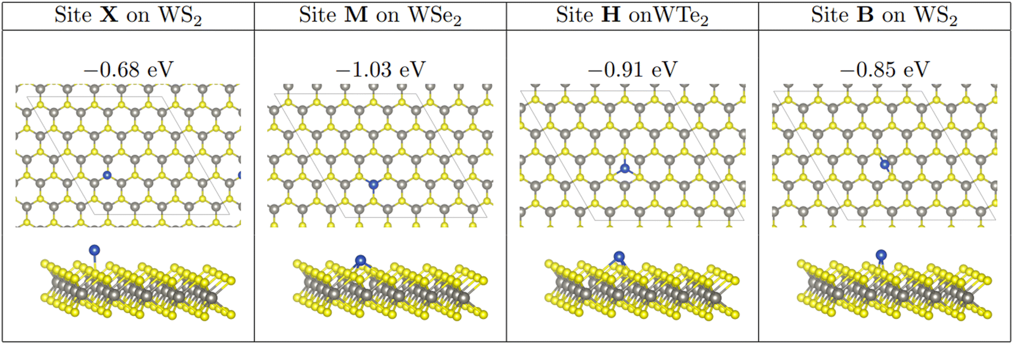 | ||
| Fig. 1 Adsorption of a single copper atom at each adsorption site. Ebind/atom shown in eV. In this and all other figures showing optimised showing optimised geometries. Although adsorption at site X is not stable, it is shown illustrate Cu placement at site X. Atomic colours are as follows: grey = W; yellow = S; blue = Cu. | ||
Due to the large number of geometries investigated (111 initial structures), we show only those directly relevant to the discussion. A complete set of figures for all optimised geometries is provided in the ESI.†
As we are interested in the morphology of adsorbed copper, we distinguish between 2D and 3D structures. A structure is considered 2D if all Cu atoms are bound to the WX2 monolayer (X being S, Se, or Te). In a 3D structure however, at least one Cu atom is not bound to the monolayer, but only to other Cu adatoms.
For the sake of clarity, structures are referred to by their initial configuration, rather than their fully relaxed configuration. Furthermore the monolayer to which metal atoms are adsorbed will be denoted by the chalcogen species as a prefix in the label, e.g. S-Neighbour-X is a Neighbouring (vide infra) configuration starting at site X on WS2. This allows for easy reference to the ESI,† which contains images for all final structures. It should be noted that due to the significant amount of adatom migration which often occurs during relaxation, the starting structure name may not describe the fully relaxed configuration. Nonetheless, this approach allows for a consistent description of copper-TMD adsorption structures. It is also important to note that different starting configurations may relax to the same final configuration, resulting in identical relaxed configurations being referred to by different initial labels.
Condensed tables of energies (Tables 2–4) are shown in this paper, where energies for the resulting configurations are referred to by a single starting structure label. This does not indicate the number of starting structures which result in the same relaxed configuration, and therefore have the same or similar energies. If identical relaxed configurations have slightly different energies, the binding energy which is the largest, and the metal–substrate and metal–metal interaction energies calculated for this binding energy are shown. Note that the largest differences in binding, metal–surface, and metal–metal energies for the same adsorption modes are 0.05, 0.04, and 0.06 eV respectively. A full table of energies for each configuration can be seen in the ESI, Tables S1–S4.†
3.1 Single atom adsorption
Single Cu atoms adsorb exothermically at each adsorption site across all three of the TMD monolayers studied; see Table 1. For all three monolayers, M is the most stable adsorption site, followed by H, B, and then X. This trend was also observed with Cu adsorption onto a monolayer of MoS2.71For single atom adsorption, increasing the number of Cu–surface bonds increases the overall stability of the adsorption. At site X, which is the least favourable site, the Cu adatom is bound to a single chalcogen atom. B, where the adatom binds to two chalcogenide atoms, is the second least stable site on each monolayer. M and H allow the Cu adatom to bond to three chalcogen atoms, and are therefore the two most stable adsorption sites for single atoms. M is likely the most stable of all four sites as the presence of an atom here is a continuation of the WX2 crystal structure. Interestingly, as the size of the chalcogen species increases, the difference in stability between M and H decreases, with the difference being 0.12, 0.08, and 0.04 eV on the sulphide, selenide, and telluride respectively.
Single atom adsorption on the WTe2 monolayer is the most energetically favourable, followed by adsorption on WS2 and then WSe2. The exception being that the X adsorption is strongest on WS2, followed by WTe2 and WSe2. It should be noted however, that the difference in stability between the three monolayers is not significant, with a typical magnitude of ∼0.10 eV.
As we have been able to disaggregate the overall adsorption energy of each cluster, we are interested in relating geometric parameters including Cu–Cu and Cu–X (X = S, Se, Te) distance, to the metal–metal and metal–surface interactions respectively. We have found that the relationship between Cu structure and metal–metal interaction energy is largely dependent on the specifics of each cluster type, whereas the relationship between Cu–X (X = S, Se, Te) bond and metal–surface interaction is not dependent on cluster type.
In general, there is no correlation between shorter bond lengths and a stronger metal–surface interaction. Rather, it is the adsorption sites that determine the metal–substrate energy. On all monolayers, single atom adsorption has a shortest Cu–X bondlength at site X, with this length increasing at sites B, M, and H respectively. These distances range from 2.19 to 2.39 Å on WS2, 2.35 to 2.55 Å on WSe2, and 2.52 to 2.67 Å on WTe2. Cu–X bond lengths for Cu adsorption presented in this work are similar to Cu2X bulk structures, with Cu2S having Cu–S bond length of 2.34 Å,89 Cu2Se have Cu–Se lengths between 2.49 and 2.51 Å,90 and Cu2Te having Cu–Te lengths between 2.61 and 2.67 Å.91
Using CI-NEB, the activation energies for Cu migration between sites X, M, and H were calculated on all three monolayers. The activation barrier to transition from M to H is essentially identical on all three monolayers, with an activation barrier of 0.16 eV on the sulphide and selenide monolayers, and 0.15 eV on the telluride monolayer. However, the activation energy to transition from H to M increases, albeit with small absolute values, as the size of the chalcogen atom increases. On WS2, WSe2, and WTe2, the barrier becomes 0.04, 0.08, and 0.12 eV respectively. This is due to the relative difference in adsorption stability between M and H decreasing as the size of the chalcogen atom increases, which can be seen from the binding energies. These low barriers suggest facile diffusion of a single Cu atom over the TMD monolayers, most likely moving between these two adsorption sites.
No transition state was found for migration from X to either M or H on any of the three monolayers, implying that the relaxed structures for single atom adsorption at site X is not a local energy minimum, but rather a saddle point. To further probe the stability of this structure, vibrational analysis was performed on the relaxed structure for single atom adsorption at X on WS2. In doing this two imaginary vibrational modes were found, with frequencies of −22.33 and −29.60 cm−1. This implies that this structure is a second order saddle point on the potential energy surface, and therefore that this geometry is unstable at finite temperature.
Finally, ab initio MD simulations were performed at 100 K to investigate the adsorption dynamics at site X. Across all three monolayers the adsorbed Cu atom migrates off site X in under 500 fs. After this, the Cu atom stays adsorbed at the H site on WS2, and M on WSe2 and WTe2. This is consistent with similar stability on these sites and moderate activation barriers for Cu migration, and further shows that site X is not a stable adsorption site for a single metal atom.
3.2 Two atom adsorption
Three different initial configurations were considered for two atom adsorption on each monolayer. The first configuration, labelled as Neighbouring, has Cu atoms adsorbed at nearest neighbour equivalent sites. The second configuration, labelled as Separated, has Cu atoms arranged at equivalent third nearest neighbour sites with no Cu–Cu bonds. The final configuration, labelled Non-Equivalent, has Cu atoms located at second nearest neighbour non-equivalent sites, in differing permutations (X–M, X–H and M–H, see Fig. 2).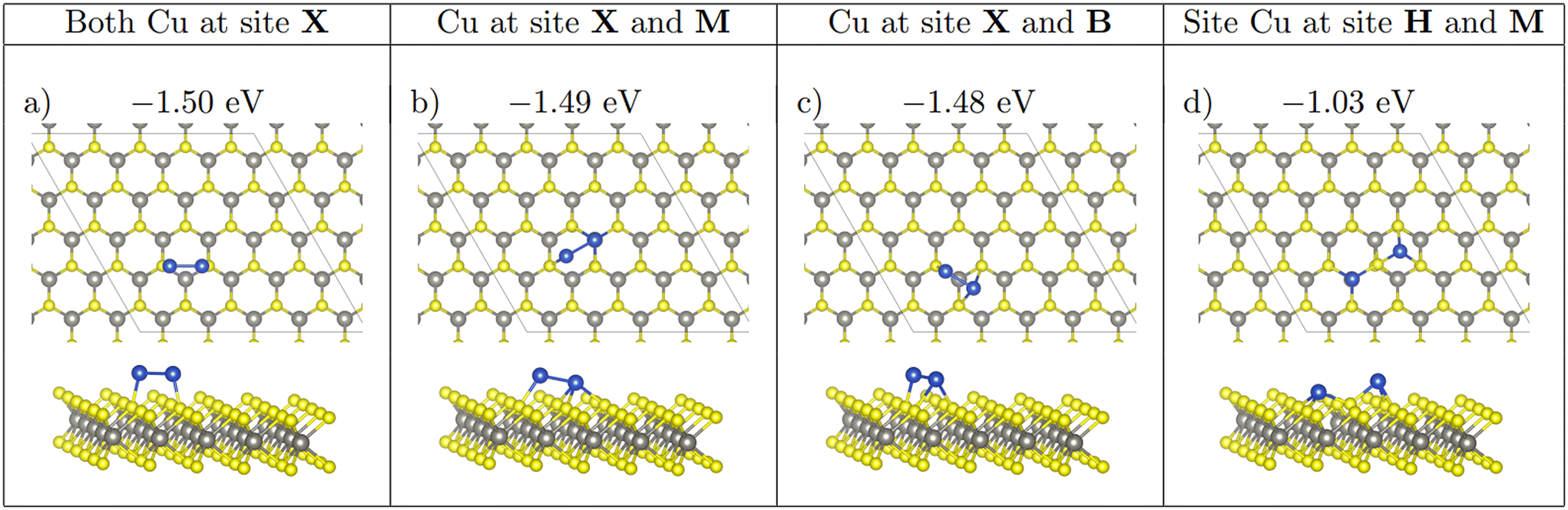 | ||
| Fig. 2 Panels (a)–(c) show the three configurations which 2 atom Cu clusters adopt. (d) Shows the local strain that adsorption at site H and M introduce to the surface. Ebind/atom shown in eV. Colour scheme is identical to that in Fig. 1. | ||
All relaxed structures are shown in Fig. S2–S4 in the ESI.†
All Neighbouring adsorption on WSe2 converge to the same adsorption mode, with both Cu atoms adsorbed above neighbouring selenium atoms. Energetically, all structures are identical on this monolayer, however, there are slight structural differences between the three configurations, where Se-Neighbour-M and Se-Neighbour-H are increasingly distorted Se-Neighbour-X structures. Although both Se-Neighbour-M and Se-Neighbour-H are more distorted than Se-Neighbour-X, the copper-copper bond length remains very similar across all three configurations. The distance between Cu atoms is 2.25, 2.26, and 2.28 Å for Se-neighbour-X, Se-Neighbour-M, and Se-Neighbour-H respectively.
The interaction between the Cu adatoms has the largest contribution to the stability of these nanocluster, with the metal–metal interaction energy comprising almost 80% of the total binding energy of these clusters (see Fig. 3 for decomposed energy plots). Therefore, a preservation of a similar Cu bond length across all three structures is unsurprising as this interaction drives the stability of the Neighbouring configurations despite clear structural differences.
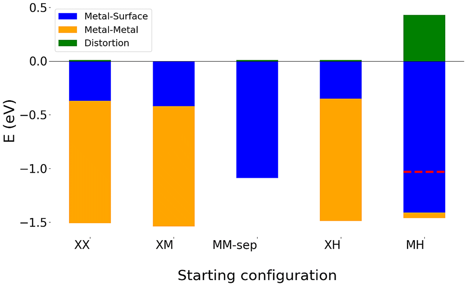 | ||
| Fig. 3 Decomposition of adsorption energy for 2 Cu atom adsorption on WS2, showing the competition between maximising metal–metal and metal–surface energies. The red dotted line denotes the overall adsorption energy for configuration MH, where the adsorbed Cu atoms strongly distort the surface. | ||
Similarly on WTe2, all Neighbouring adsorption configurations relax to the configuration where Cu atoms initially present at both M and H sites migrate to adsorb above the chalcogen site, site X. As with both the sulphide and selenide monolayer, all neighbouring adsorption modes have the same binding energy on each respective monolayer. Similar to single atom adsorption, the difference in stability between the three monolayers is within the range of 0.10 eV. This shows that the chalcogen species does not have a significant effect on the adsorption stability.
S-Neighbour-M forms the second structure seen in the Neighbouring adsorption. This structure is unstable and relaxes to the non-equivalent configuration S-Non-Equivalent-XM. For the S-Neighbour-M relaxation, one of the Cu atoms remains adsorbed at M while the second Cu atom migrates to X. This migration likely occurs to reduce the distance between both adsorbed Cu atoms, which then increases the stability of the nanocluster due to the formation of a Cu–Cu bond. The formation of this bond of course also increases the metal–metal interaction energy. The distance between both Cu atoms is ∼0.1 Å larger than the other Neighbouring structure. This small difference means the structures have identical energies.
The inter-copper distances for these clusters are smaller than in bulk elemental copper. This is due to the nature of the interaction of the cluster with the monolayer, combined with the size of the Cu cluster. Previous work on the properties of copper clusters has shown that a Cu dimer in vacuum is expected to have an inter-copper distance of 2.25 Å.92 As the adsorbed 2 atom clusters are not interacting strongly with the monolayers, their dimer structure does not deviate largely from that of a Cu dimer in vacuum.
For all 2 atom clusters, the Cu–Cu distances of the Cu dimers vary by only ±0.09 Å, from 2.25 Å to 2.34 Å. Similarly, the range of metal–metal interaction energies for the Cu dimers is quite small, all energies are within 0.02 eV (−1.12 to −1.14 eV). Although bond strength and bond length can be correlated, in considering the 15 Cu dimer adsorption structures on the three TMDs, there is no clear correlation between inter-copper bond lengths and the computed metal interaction energies. This is likely due to the extremely small ranges of bond lengths and metal–metal energies for these dimers. Moreover, the inter-copper distance is independent of the WX2 monolayer on which these Cu dimers are adsorbed.
Cu–X distances are between 2.25 and 2.44 Å on WS2, 2.40 and 2.57 Å on WSe2, 2.56 and 2.69 Å on WTe2 for Cu2 adsorption.
Similar to Cu1 adsorption, Separated configurations are most stable on WTe2, then WS2 and WSe2. However, on the WTe2 monolayer there is no longer any difference in stability between atoms adsorbed at M and H.
On all three monolayers, Non-Equivalent configuration Non-Equivalent-XM forms the same structure as the configuration S-Neighbouring-M on WS2. The metal–metal interaction energy for these Non-Equivalent-XM clusters are identical on all three monolayers. The binding energy follows the same stability trend as single atom adsorption, due to the metal–substrate interaction energies being largest on WTe2 and smallest on WSe2.
For the configuration Non-Equivalent-MH, both adsorbed Cu atoms do not migrate during relaxation on all three of the monolayers. The binding energy of this adsorption mode is comparable to that of the Separated adsorption at M and H, due to the fact that Cu atoms do not agglomerate to form copper–copper bonds. This can be seen from the negligible metal–metal interaction energy of this configuration across all three monolayers.
On each monolayer, the metal–substrate interaction of Non-equivalent-MH is larger than the binding energy. This arises from the distortion term, Edistortion, being larger than the metal–metal interaction energy for this configuration on all monolayers. This distortion is caused by both Cu adatoms being bonded to the same chalcogen, which lies between both Cu adsorption sites. Although this is seen on both the selenide and telluride monolayer, the monolayer is not strained to the same extent. The increased atomic radius of both selenium and tellurium, compared to sulphur means that much less strain is put on the monolayer in order to accommodate this adsorption mode. This is evident from small Edistortion of only 0.08 and 0.10 on WSe2 and WTe2, compared to 0.43 eV on WS2. Interestingly, although the Cu–chalcogen bonds are longest on the WTe2 monolayer, the distortion caused by the adsorbed atoms is slightly larger than that on the WSe2 monolayers, again showing that despite an increased distance between Cu and chalcogen atoms on WTe2, the interaction is slightly stronger than that on WSe2.
In general, it is clear that the final adsorption site does not have a large effect on the stability of the Cu cluster, but rather the presence (or absence) of copper–copper bonds determines the stability of the structure on the TMD monolayers. The presence or absence of copper–copper bonds is however largely determined by initial adsorption site so that the initial adsorption site does play a role in determining final cluster stability. Furthermore, there is still a small difference (typically <0.2 eV) in stability between identical structures on the three different monolayers, with WTe2 forming the most stable adsorption, and WSe2 forming the least stable. This indicates that the effect of the chalcogen on adsorption energy is minimal.
3.3 Cu3 and Cu4 adsorption
Four initial configurations were considered for adsorption of three atoms: three configurations are initially 2D and the fourth is a 3D structure. The three 2D structures are indicated as Line, Offset (Fig. 4), and Triangle, whereas the 3D structure is labelled as 3D-Triangle. Four initial configurations were also considered for Cu4. Two structures are initially 2D, and the remaining two structures are initially 3D. The two 2D structures are labelled as Wire and Rhombus, while the 3D configurations are labelled as 3D-Rectangle and Tetrahedron. Fig. 5 shows select relaxed Cu4 clusters. All relaxed structures for Cu3 and Cu4 are shown in Fig. S5–S11 in the ESI.†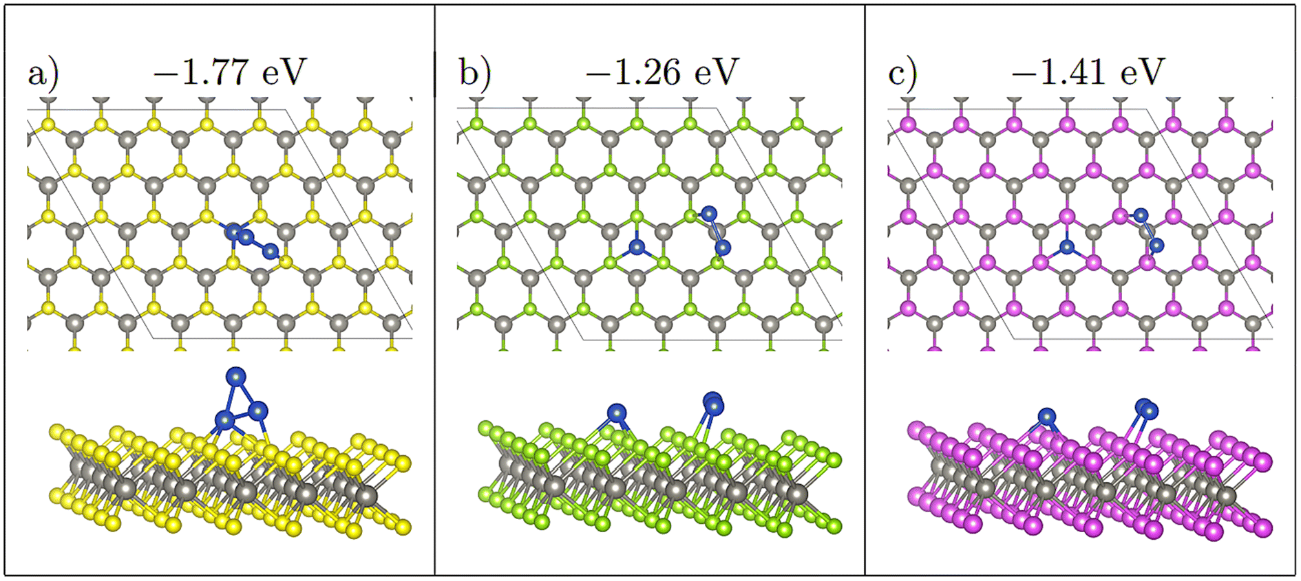 | ||
| Fig. 4 Comparing Offset adsorption for Cu3, initially at site H on all three monolayers. Note that on WS2 (a), the three Cu atoms agglomerate to form a 3D triangular structure. On WSe2 (b) and WTe2 (c) the two neighbouring Cu atoms migrate to be adsorbed atop chalcogen atoms. Ebind/atom shown in eV. Colour scheme as in Fig. 1, furthermore, green = Se; purple = Te. | ||
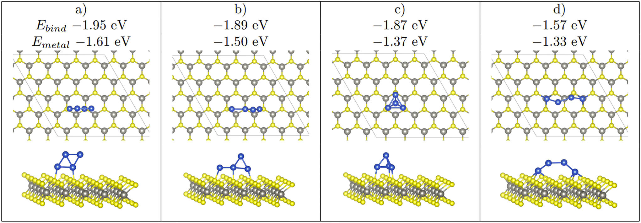 | ||
| Fig. 5 The 4 stable Cu4 clusters found upon relaxation on WX2. From left to right the most stable to least stable structure (a > b > c > d). Note that the binding energy, and the metal–metal interaction energy is shown. Furthermore, a 2D adsorption mode of the Cu4 cluster seen in (a) is also a stable structure, whereas (b)–(d) only appear as 3D strucutres. Colour scheme as in Fig. 1. | ||
A clear preference for 3D structures over 2D structures is shown in relaxed Cu3 and Cu4 adsorption configurations. There are a combined 72 starting configurations, 45 of which are initially 2D structures. Once fully relaxed however, only 24 structures remain 2D. 11 Cu3 structures transition from 2D to 3D and 10 Cu4 structures transition from 2D to 3D, with none of the 72 configurations transitioning from 3D to 2D. Of the 24 structures which remain 2D, only 11 of them contain an intact Cu cluster (3 or more Cu atoms in a single cluster). The remaining 13 structures are comprised of separated Cu1 and Cu2 structures adsorbed on the monolayer.
For Cu3 configurations, only 1 three-atom Cu cluster type emerges, that being a triangular structure. For Cu4 structures however, 4 four-atom Cu cluster types emerge (see Fig. 5). For both Cu3 and Cu4 relaxations, clusters of the same type (i.e. same inter-copper arrangements) can differ by both adsorption site and whether or not they have a 2D or 3D morphology. As discussed vide infra, the arrangement of Cu atoms with respect to each other, rather than with respect to the monolayer, is the main factor driving adsorption stability.
In comparing configurations with Cu3 and Cu4 atom clusters to Cu1 and Cu2 atom clusters, the competition between maximising metal–surface interaction energy and metal–metal interaction energy becomes more prominent. Similar to 1 and 2 atom adsorption, configurations with 3 and 4 Cu atoms which maximise the metal–metal interaction energy are the most stable adsorption structures. Therefore, it is unsurprising that Cu3 and Cu4 configurations which relax to two atom and single atom adsorption (such as Te-Wire-H, see Fig. S10†) are the least stable configurations, due to their smaller metal–metal interaction energies.
It is interesting to note that these 2D structures, while having a smaller binding energy and metal–metal interaction energy than the 3 and 4 atom clusters, have a larger metal–surface interaction energy.
There is competition between maximising metal–surface energies and metal–metal energies. However, the magnitude of metal–metal interaction energies is much larger than that of metal–surface energies, with the largest metal–surface energy being −0.85 eV (Te-Wire-H) and the largest metal–metal interaction energy being −1.61 eV (S-Rhombus-X).
This competition is most clearly seen with the Offset structure S-Offset-H (Fig. 4), which has large atomic migrations, relaxing to a 3D 3-atom structure. During relaxation the single separated atom is initially stable, whereas the two atom cluster which was initially adsorbed at H migrates to neighbouring sulphide atoms. In the formation of this cluster, the distance between the two atom cluster and the single atom decreases. Once this distance becomes ∼3.3 Å the single Cu atom begins to migrate away from the initially stable H site to form a 3 atom cluster. Once this three atom cluster forms, the central Cu atom rises upwards to form a 3D triangle structure (Fig. 4(a)).
This shows that once Cu atoms are within ∼3 Å, the increase in stability caused by the formation of Cu bonds is stronger than Cu interaction with the monolayer. On WSe2 and WTe2 the distance between the single Cu atom and the two atom cluster for Offset-H has a minimum distance of 4.97 and 5.41 Å respectively, which is likely why a 3D structure does not form here.
Although there is a clear preference for 3D morphology in Cu3/Cu4 relaxations, the difference in stability between 2D and 3D clusters is not significant at this cluster size. Rather, the preference for 3D morphology is evident from the number of 3D structures after relaxation, and the larger magnitude of metal–metal interaction energies compared to metal–surface energies. For example, all Cu3 which have 3 Cu atoms in a single cluster have very similar binding energy, regardless of whether they are 2D or 3D (typically less than 0.20 eV difference). This is due to the fact that these configurations form the same copper triangle structure. These configurations then have the same metal–metal interaction energy of about −1.24 eV. As discussed, the metal–metal interaction energy is the largest contributor to binding energy and so overall there will not be any significant differences in stability for these clusters whether adsorbed 2D or 3D onWX2. Although, as discussed in the introduction a metal–metal interaction energy which is larger than the metal–surface interaction energy, will contribute to 3D growth. It should be noted that this triangular structure takes a C2v symmetry structure, which is the ground state configuration of a neutral three atom Cu cluster in the gas phase.92 The weaker metal–surface interaction presumably permits this cluster structure to be particularly stable.
A noticeable exception to this however is Se-Triangle-M (see Fig. 6). This structure has a dramatically reduced metal–surface interaction energy, and forms the least stable of all Triangle structures. The metal–substrate energy, is ∼0.2 eV less for Se-Triangle-M compared to the other stable structure on the selenide monolayer, whereas typical variations in metal–surface energies due to changing adsorption site are less than 0.10 eV. In Se-Triangle-M, all three Cu atoms migrate to coordinate above a single selenide atom, while remaining in a 2D triangle structure, which is not seen on either the WS2 or WTe2 monolayer. On WS2 the sulphur atom is likely not large enough to allow for coordination with three Cu atoms at once, while the Te species is too large to allow this coordination.
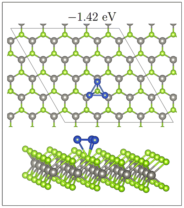 | ||
| Fig. 6 Triangular Cu structure adsorbed to a single selenide atom onWSe2. Ebind/atom shown in eV. | ||
For this adsorption, there is a markedly reduced metal–substrate energy and an uncharacteristically long Cu–X bond length (∼2.77 Å compared to ∼2.35 Å). For all other Cu3 structures, Cu–X bond lengths and metal–substrate energies do not deviate from those in Cu1 or Cu2 adsorption.
As with 2 atom clusters, we are interested in relating geometric parameters to metal–metal and metal–surface energies. For clusters in which three Cu atoms are bonded, all of which form a triangular structure, there is a clear correlation between (mean) bond length in the cluster and metal–metal interaction energy. The mean Cu–Cu distance is calculated as the average of the three Cu–Cu distances in the Cu triangle. We find that as the Cu–Cu distance increases, the metal–metal interaction energy decreases. We believe that this trend is observed for three atom clusters due the larger range of Cu–Cu distances and metal interaction energies for these clusters: Cu–Cu distances have a range of 0.30 Å(2.36 to 2.66 Å) and the metal interaction energies have a range of 0.06 eV (−1.19 to −1.25 eV).
This is a larger variation compared to 2 atom clusters which arises due to the 3D triangle structures that form on WTe2. As the lattice constant of WTe2 is much larger than that of WSe2 and WS2, the distance between the two Cu atoms adsorbed directly to the surface significantly increases (to ∼3.2 Å) compared to the 2D triangles on WTe2 (∼2.3 Å) or any of the triangle structures on WS2 and WSe2, which have Cu–Cu distances of ∼2.3 Å.
If only the 2D triangle clusters are considered, there is now no clear correlation between mean bond length and metal–metal energy. This is due to the fact that the ranges for both mean bond lengths and metal–metal energy are too small to show any effect (ranges 0.11 Å, 0.02 eV). Moreover, similar to 2 atom adsorption, the monolayer on which these Cu dimers are adsorbed on does not affect the inter-copper distance of 2D triangles (or 3D triangles on WSe2 and WS2).
Although generally the adsorption sites do not notably affect the stability of the adsorbed cluster, not all adsorption sites are equally stable. For example, site H is typically an unstable site for multiatom adsorption; of the 24 configurations initially adsorbed on this site, only 1 multiatom structures fully relaxes to be adsorbed at this site, Te-3DRectangle-H.
As previously mentioned, 4 atom Cu clusters show a greater preference for 3D growth than 3 atom clusters. Unlike Cu3, where there is only 1 distinct copper structure, that being a triangular structure (both 2D and 3D), there are 4 unique 4 atom Cu clusters (see Fig. 5). Similarly to 3 atom clusters, the most stable of these structures are the rhombic structures that resemble the D2h ground state configuration of a neutral four atom Cu cluster in gas phase.92 Both 2D and 3D structures in which copper atoms arrange in this manner have the largest metal–metal interaction energies of all copper adsorption structures. It is also interesting to note that all adsorption modes with this structure are adsorbed at the chalcogen site.
For rhombic Cu4 adsorption structures there is no clear correlation between mean bond length and metal–metal energy. This is likely due to the narrow range of average Cu–Cu distances (2.37 to 2.39 Å) for these structures, the variation in the metal–metal energies is also small, at 0.10 eV. However, two distinct rhombic structures appear; these are either buckled or unbuckled. As seen in the Fig. 7, there is a clear correlation between “buckling” of these clusters, quantified by the dihedral angle (see Fig. S13† for description of how this angle is measured), and the metal–metal energy.
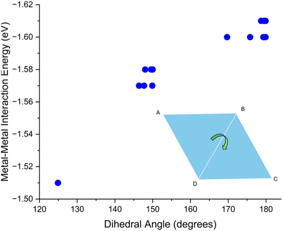 | ||
| Fig. 7 Computed metal–metal interaction energy vs. dihedral angle of all rhombic structures. The graphic in the bottom right displays dihedral angle (see Fig. S13†). | ||
Once this dihedral angle decreases to less than 180°, the metal–metal energy of these clusters decreases. This is expected, as the ground state of this rhombic cluster in vacuum has a 2D structure, and any distortion of the geometry reduces the interaction energy.
The Cu–Cu distances and metal–metal interaction energies for the remaining 15 Cu4 clusters do not have sufficient variation in both the metal interaction energy and the mean Cu–Cu distance, or a large enough number of structures to be able to draw meaningful correlation between geometric factors and metal interaction energies within each cluster type.
As with Cu1, Cu2, and Cu3 adsorption, it is the adsorption site that determines the magnitude of the metal–surface energy, not the Cu–X distance. With adsorption at site X corresponding to the smallest metal–surface energies and shortest bond lengths (between 2.16 and 2.32 Å on WS2, 2.30 and 2.53 Å on WSe2, and 2.46 to 2.67 Å on WTe2). Moreover, the largest Cu–X distances are found in clusters that adsorb at site M, which also have the largest metal–substrate energies (2.29 to 2.46 Å on WS2; 2.42 to 2.56 Å on WSe2; 2.56 to 2.80 Å on WTe2). It is interesting to note that no Cu–X bond length for Cu1, Cu2, or Cu3 adsorption lies outside the ranges also seen in Cu4 adsorption.
The other stable structures are discussed in the ESI.†
To further investigate the preference for either 2D or 3D Cun structures on the TMDs, CI-NEBs were performed to find the energy barrier when transitioning from 2D rhombic structures to a 3D tetrahedral structure, where both structures are adsorbed to the monolayer at X and a copper atom bound to the TMD migrates to the apex of the tetrahedral cluster. On WS2 and WSe2 the computed activation barriers are 0.30 eV and 0.37 eV. The activation barrier to transition from the 3D tetrahedral structure to the 2D rhombic structure, that is Cu migration onto the TMD, is 0.06 and 0.07 eV on the sulphide and selenide, respectively. This is consistent with the 2D rhombic cluster being more stable than the tetrahedral structure. Thus the activation barriers between different structures on these TMD monolayers are relatively small, consistent with the relatively weak copper–surface interactions. On the telluride monolayer, no transition state was found, implying that the tetrahedral structure is possibly a saddle point. It should be noted however that one configuration which began as a tetrahedral structure on WTe2, relaxed to a rhombic structure with three Cu atoms adsorbed to the surface (see Fig. S10†).
4 Conclusion
Understanding how metal species behave, and what adsorption structures they form on transition metal dichalcogenides is important for targered material design for many technologies including catalysis, sensors and next generation transistors. We have presented an extensive first principles DFT study on the interaction of Cun clusters, with n = 1–4, on monolayers of the TMDs WS2, WSe2, and WTe2, which show great promise for many applications. The interaction of Cu with these monolayers at the sub-nanometre scale is required in order to understand the fundamental interactions between Cu and WX2 monolayers, and their role in nucleation of metal films. By investigating these interactions on three different TMD substrates, the role of the chalcogen in these interactions can also be understood. Furthermore, comparing these results to previous work on MoS2 can reveal the role of the metal species of the TMD.We find that single atom adsorption follows the same trends seen on MoS2,71 with absorption above W more favourable than adsorption at any other site. Adsorption on the telluride monolayer is the most stable, followed by adsorption on the sulphide and then selenide monolayer; however this difference in energy is typically less than 0.10 eV. Furthermore, the adsorption energies on WX2 monolayers differ typically by less than 0.10 eV compared to identical adsorption modes on an MoS2 monolayer.71
For multiatom adsorption structures, the metal–metal interaction is the dominant driving force for cluster stability. By contrast, the metal–surface interaction energy has a significantly smaller magnitude, and thus impact on all adsorption configurations.
The weakest metal–substrate energies are found with configurations that adsorb at site X, which have the shortest Cu–X lengths. Moreover, the largest Cu–X distances are found in clusters that adsorb at site M, which also have the largest metal–substrate energies. The number of bonds that the adsorbed atom forms with the monolayer is correlated to adsorption stability (particularly for single atom adsorption), with site M and H forming three bonds and being the most stable, and site X forming one bond and being the least stable. Furthermore, Cu–X distances for nanocluster adsorption is comparable to Cu–X distances in bulk Cu2X for all monolayers.
A preference for 3D morphology is shown on all three monolayers, likely as this makes it possible to maximise metal–metal interaction energy by maximising the number of Cu–Cu bonds and reducing the Cu–Cu distance in each bond. This is also likely why, as seen on MoS2, as the cluster size increases, clusters prefer to adsorb above the chalcogen site, even though this is the least stable site for single atom adsorption.
Although a clear preference for 3D structures is shown, whether or not a structure is 2D or 3D tends not to determine the magnitude of its stability, but rather the geometry of the Cu cluster determines final stability. Multiatom clusters that form geometries closest to the structure of ground state Cun clusters in vacuum form the most stable adsorption configurations.
Furthermore, both the chalcogen present in the monolayer, and the site to which the Cun structure is adsorbed does not have a major effect in determining the final stability on any of the monolayers presented in this study.
CI-NEB results shown that migration barriers between adsorption structures on TMDs tend to be quite small across all three monolayers. In addition, many relaxations resulted in large migrations of Cu across the monolayer. This implies that motion of both single Cu atoms and Cu nanoclusters is likely to be dynamic at finite temperature. This dynamic and facile motion of metal atoms on WX2 at finite temperature may significantly affect deposition and growth processes, and will be subject of further study.
Data availability
The data supporting this article have been included as part of the ESI† and can be obtained from https://doi.org/10.5281/zenodo.13992536.Conflicts of interest
There are no conflicts to declare.Acknowledgements
The research conducted in this publication was funded by Research Ireland (formerly Irish Research Council) under grant number GOIPG/2023/4025 (IRC Government of Ireland Postgraduate Scholarship, held by M. S.). Michael Nolan is receiving support by the European Union through the ASCENT+ program grant agreement number 871130. Cara-Lena Nies and Michael Nolan have received support from SFI-NSF China Partnership program, Grant Number 17/NSFC/5279. We acknowledge support from the Irish Centre for High End Computing (ICHEC) for access to the Meluxina computing facilities.References
- K. S. Novoselov, A. K. Geim, S. V. Morozov, D. Jiang, Y. Zhang, S. V. Dubonos, I. V. Grigorieva and A. A. Firsov, Science, 2004, 306, 666–669 CrossRef CAS PubMed.
- M. J. Allen, V. C. Tung and R. B. Kaner, Chem. Rev., 2010, 110, 132–145 Search PubMed.
- V. B. Mbayachi, E. Ndayiragije, T. Sammani, S. Taj, E. R. Mbuta and A. Ullah Khan, Results Chem., 2021, 3, 100163 Search PubMed.
- R. M. Ronchi, J. T. Arantes and S. F. Santos, Ceram. Int., 2019, 45, 18167–18188 CrossRef CAS.
- Y. Gogotsi and B. Anasori, ACS Nano, 2019, 13, 8491–8494 CrossRef CAS.
- K. Zhang, Y. Feng, F. Wang, Z. Yang and J. Wang, J. Mater. Chem. C, 2017, 5, 11992 RSC.
- M. Chhowalla, H. S. Shin, G. Eda, L. J. Li, K. P. Loh and H. Zhang, Nat. Chem., 2013, 5, 263–275 CrossRef PubMed.
- D. Xiao, G. B. Liu, W. Feng, X. Xu and W. Yao, Phys. Rev. Lett., 2012, 108, 196802 CrossRef PubMed.
- C. Cong, J. Shang, Y. Wang and T. Yu, Adv. Opt. Mater., 2018, 6, 1700767 CrossRef.
- K. F. Mak, C. Lee, J. Hone, J. Shan and T. F. Heinz, Phys. Rev. Lett., 2010, 105, 136805 CrossRef PubMed.
- K. F. Mak, K. He, C. Lee, G. H. Lee, J. Hone, T. F. Heinz and J. Shan, Nat. Mater., 2013, 12, 207–211 CrossRef CAS PubMed.
- B. Radisavljevic, A. Radenovic, J. Brivio, V. Giacometti and A. Kis, Nat. Nanotechnol., 2011, 6, 147–150 CrossRef CAS.
- O. Lopez-Sanchez, D. Lembke, M. Kayci, A. Radenovic and A. Kis, Nat. Nanotechnol., 2013, 8, 497–501 CrossRef CAS PubMed.
- J. Pu, Y. Yomogida, K.-K. Liu, L.-J. Li, Y. Iwasa and T. Takenobu, Nano Lett., 2012, 12, 4013–4017 CrossRef CAS PubMed.
- S. Bertolazzi, J. Brivio and A. Kis, ACS Nano, 2011, 5, 9703–9709 CrossRef CAS PubMed.
- I. Kaplan-Ashiri, S. R. Cohen, K. Gartsman, V. Ivanovskaya, T. Heine, G. Seifert, I. Wiesel, H. D. Wagner and R. Tenne, Proc. Natl. Acad. Sci. U. S. A., 2006, 103, 523–528 CrossRef CAS.
- A. Splendiani, L. Sun, Y. Zhang, T. Li, J. Kim, C. Y. Chim, G. Galli and F. Wang, Nano Lett., 2010, 10, 1271–1275 CrossRef CAS PubMed.
- T. Korn, S. Heydrich, M. Hirmer, J. Schmutzler and C. Schller, Appl. Phys. Lett., 2011, 99, 102109 CrossRef.
- W. Zhao, Z. Ghorannevis, L. Chu, M. Toh, C. Kloc, P. H. Tan and G. Eda, ACS Nano, 2013, 7, 791–797 CrossRef CAS.
- J. F. Silveira, R. Besse and J. L. D. Silva, ACS Appl. Electron. Mater., 2021, 3, 1671–1680 CrossRef CAS.
- S. Suga, C. Tusche, Y. I. Matsushita, M. Ellguth, A. Irizawa and J. Kirschner, New J. Phys., 2015, 17, 083010 CrossRef.
- A. Ghafari, L. Petaccia and C. Janowitz, Appl. Surf. Sci., 2017, 396, 1649–1656 CrossRef CAS.
- D. Voiry, H. Yamaguchi, J. Li, R. Silva, D. C. Alves, T. Fujita, M. Chen, T. Asefa, V. B. Shenoy, G. Eda and M. Chhowalla, Nat. Mater., 2013, 12, 850–855 CrossRef CAS.
- C. Tsai, K. Chan, F. Abild-Pedersen and J. K. Nørskov, Phys. Chem. Chem. Phys., 2014, 16, 13156 RSC.
- H. Kwon, B. Ji, D. Bae, J.-H. Lee, H. J. Park, D. H. Kim, Y.-M. Kim, Y.-W. Son, H. Yang and S. Cho, Appl. Surf. Sci., 2020, 515, 145972 CrossRef CAS.
- Q. Wang, Q. Zhang, X. Luo, J. Wang, R. Zhu, Q. Liang, L. Zhang, J. Z. Yong, C. P. Y. Wong, G. Eda, J. H. Smet and A. T. Wee, ACS Appl. Mater. Interfaces, 2020, 12, 45235–45242 CrossRef CAS.
- J. Barot, S. Gupta and P. Gajjar, Mater. Today: Proc., 2023 DOI:10.1016/j.matpr.2023.01.191.
- F. Godel, V. Zatko, C. Carrétéro, A. Sander, M. Galbiati, A. Vecchiola, P. Brus, O. Bezencenet, B. Servet, M. B. Martin, B. Dlubak and P. Seneor, ACS Appl. Nano Mater., 2020, 3, 7908–7916 CrossRef CAS.
- Z. Wang, L. Zhao, K. F. Mak and J. Shan, Nano Lett., 2017, 17, 740–746 CrossRef CAS PubMed.
- T. Xu, Y. Liu, Y. Pei, Y. Chen, Z. Jiang, Z. Shi, J. Xu, D. Wu, Y. Tian and X. Li, Sens. Actuators, B, 2018, 259, 789–796 CrossRef CAS.
- R. Guo, Y. Han, C. Su, X. Chen, M. Zeng, N. Hu, Y. Su, Z. Zhou, H. Wei and Z. Yang, Sens. Actuators, B, 2019, 300, 127013 CrossRef CAS.
- R. K. Jha and N. Bhat, Adv. Mater. Interfaces, 2020, 7, 1901992 CrossRef CAS.
- X. Liu, G. Duan, W. Li, Z. Zhou and R. Zhou, RSC Adv., 2017, 7, 37873–37880 RSC.
- Y. So, D. B. Yim, S. Lee, H. Lee, H. Kim, Y. Yu, C. Choi and J. H. Kim, Chem. Eng. J., 2023, 468, 143727 CrossRef CAS.
- Y. Gao, Z. Liu, D. M. Sun, L. Huang, L. P. Ma, L. C. Yin, T. Ma, Z. Zhang, X. L. Ma, L. M. Peng, H. M. Cheng and W. Ren, Nat. Commun., 2015, 6, 8569 CrossRef CAS PubMed.
- X. Zhang, T. H. Choudhury, M. Chubarov, Y. Xiang, B. Jariwala, F. Zhang, N. Alem, G.-C. Wang, J. A. Robinson and J. M. Redwing, Nano Lett., 2018, 18, 1049–1056 CrossRef CAS.
- J. Zhou, F. Liu, J. Lin, X. Huang, J. Xia, B. Zhang, Q. Zeng, H. Wang, C. Zhu, L. Niu, X. Wang, W. Fu, P. Yu, T. R. Chang, C. H. Hsu, D. Wu, H. T. Jeng, Y. Huang, H. Lin, Z. Shen, C. Yang, L. Lu, K. Suenaga, W. Zhou, S. T. Pantelides, G. Liu and Z. Liu, Adv. Mater., 2017, 29, 1603471 CrossRef PubMed.
- S. Balasubramanyam, M. J. Merkx, M. A. Verheijen, W. M. Kessels, A. J. Mackus and A. A. Bol, ACS Mater. Lett., 2020, 2, 511–518 CrossRef CAS PubMed.
- K. Park, Y. Kim, J. G. Song, S. J. Kim, C. Wanlee, G. H. Ryu, Z. Lee, J. Park and H. Kim, 2D Mater., 2016, 3, 014004 CrossRef.
- Q. Zhang, L. Mei, X. Cao, Y. Tang and Z. Zeng, J. Mater. Chem. A, 2020, 8, 15417–15444 RSC.
- K. Sarakinos, A review on morphological evolution of thin metal films on weakly-interacting substrates, 2019 Search PubMed.
- O. van der Straten, Y. Zhu, J. Rullan, K. Dunn and A. E. Kaloyeros, J. Mater. Res., 2006, 21, 255–262 CrossRef CAS.
- C.-L. Lo, K. K. H. Smithe, R. Mehta, S. Chugh, E. Pop and Z. Chen, 2017 IEEE International Reliability Physics Symposium (IRPS), 2017, pp. MR-4.1–MR-4.4.
- C. L. Lo, M. Catalano, K. K. Smithe, L. Wang, S. Zhang, E. Pop, M. J. Kim and Z. Chen, npj 2D Mater. Appl., 2017, 1, 42 CrossRef.
- K. K. Smithe, Z. Zhu, C. S. Bailey, E. Pop and A. Yoon, IEEE Int. Reliab. Phys. Symp. Proc., 2018, P-PI.1-1–P-PI.1-4 Search PubMed.
- C. L. Lo, K. Zhang, R. S. Smith, K. Shah, J. A. Robinson and Z. Chen, IEEE Electron Device Lett., 2018, 39, 873–876 CAS.
- J. S. H. Deijkers, A. A. de Jong, M. J. Mattinen, J. J. Schulpen, M. A. Verheijen, H. Sprey, J. W. Maes, W. E. M. Kessels, A. A. Bol and A. J. Mackus, Adv. Mater. Interfaces, 2023, 10, 2202426 CrossRef CAS.
- Y. Li, Q. Liu and W. Shen, Dalton Trans., 2011, 40, 5811–5826 RSC.
- Q. Lu, Y. Yu, Q. Ma, B. Chen and H. Zhang, Adv. Mater., 2016, 28, 1917–1933 CrossRef CAS.
- J. Zhu, R. Yang and G. Zhang, ChemPhysMater, 2022, 1, 102–111 CrossRef.
- S. Zhao, R. Jin, Y. Song, H. Zhang, S. D. House, J. C. Yang and R. Jin, Small, 2017, 13, 1701519 CrossRef PubMed.
- M. P. Aparna and R. Chatanathodi, Int. J. Hydrogen Energy, 2024, 51, 41–51 CrossRef CAS.
- C. Poornimadevi, C. P. Kala and D. J. Thiruvadigal, Mater. Sci. Semicond. Process., 2023, 157, 107339 CrossRef CAS.
- L. Y. Xie and J. M. Zhang, Superlattices Microstruct., 2016, 98, 148–157 CrossRef CAS.
- M. Luo, S. Y. Hao and Y. T. Ling, AIP Adv., 2016, 6, 085112 CrossRef.
- E. Pavoni, E. Mohebbi, G. M. Zampa, P. Stipa, L. Pierantoni, E. Laudadio and D. Mencarelli, Mater. Adv., 2023, 5, 2230–2237 RSC.
- X. Zhang, J. Wang, D. Chen and L. Liu, Mater. Today Commun., 2021, 28, 102488 CrossRef CAS.
- F. Li, F. Chen, H. Cui and X. Jiang, Comput. Theor. Chem., 2023, 1226, 114187 CrossRef CAS.
- H. Zhang, W. Zhou, J. Jiang, W. Zeng and Q. Zhou, ACS Appl. Nano Mater., 2024, 7, 3379–13391 Search PubMed.
- Y. C. Lin, D. O. Dumcenco, H. P. Komsa, Y. Niimi, A. V. Krasheninnikov, Y. S. Huang and K. Suenaga, Adv. Mater., 2014, 26, 2857–2861 CrossRef CAS PubMed.
- Y. Ding, Y. Wang, J. Ni, L. Shi, S. Shi and W. Tang, Phys. B, 2011, 406, 2254–2260 CrossRef CAS.
- Z. G. Majd, S. F. Taghizadeh, P. Amiri and B. Vaseghi, J. Magn. Magn. Mater., 2019, 481, 129–135 CrossRef CAS.
- H. Chen, Y. Chen, Y. Cui, S. Ren and X. Chen, Theor. Chem. Acc., 2024, 143, 32 Search PubMed.
- P. E. Evans, T. Komesu, E. F. Schwier, S. Kumar, K. Shimada and P. A. Dowben, J. Phys.:Condens. Matter, 2020, 32, 465001 CrossRef CAS PubMed.
- K. Yang, Z. Cui, E. Li, Y. Shen, L. Zhang, D. Ma, Z. Yuan, Y. Dong and S. Zhang, Chem. Phys., 2023, 571, 111903 CrossRef CAS.
- S. Guo, Y. Wang and J. Zhang, J. Phys. D: Appl. Phys., 2020, 53, 384001 CrossRef CAS.
- K. Sarvazad, M. Elahi, F. Ahmadian and A. Boochani, Mater. Res. Express, 2019, 6, 075029 CrossRef CAS.
- Z. Chen, X. Zhang, H. Xiong, D. Chen, H. Cheng, J. Tang, Y. Tian and S. Xiao, IEEE Access, 2019, 7, 72012–72019 Search PubMed.
- J. Ni, W. Wang, M. Quintana, F. Jia and S. Song, Appl. Surf. Sci., 2020, 514, 145911 CrossRef CAS.
- Z. Xu, H. Cui and G. Zhang, ACS Omega, 2023, 8, 4244–4250 CrossRef CAS PubMed.
- C. L. Nies and M. Nolan, Beilstein J. Nanotechnol., 2020, 11, 391–406 CrossRef CAS PubMed.
- C. L. Nies and M. Nolan, Beilstein J. Nanotechnol., 2021, 12, 704–724 CrossRef CAS PubMed.
- C.-L. Nies and M. Nolan, J. Phys.: Mater., 2023, 6, 035008 CAS.
- S. K. Natarajan, C. L. Nies and M. Nolan, J. Chem. Phys., 2020, 152, 144701 CrossRef.
- X. Liu, C. Z. Wang, M. Hupalo, W. C. Lu, M. C. Tringides, Y. X. Yao and K. M. Ho, Phys. Chem. Chem. Phys., 2012, 14, 9157–9166 RSC.
- G. Kresse and J. Furthmüller, Phys. Rev. B: Condens. Matter Mater. Phys., 1996, 54, 11169–11186 CrossRef CAS PubMed.
- J. P. Perdew, K. Burke and M. Ernzerhof, Phys. Rev. Lett., 1996, 77, 3865–3868 CrossRef CAS PubMed.
- P. E. Blöchl, Phys. Rev. B: Condens. Matter Mater. Phys., 1994, 50, 17953–17979 CrossRef PubMed.
- W. Xu, J. Mater. Sci. Chem. Eng., 2016, 04, 32–41 CAS.
- C. Yang, X. Zhao, T. Wang and S. Wei, J. Alloys Compd., 2017, 699, 291–296 CrossRef CAS.
- W. G. Dawson and D. W. Bullett, J. Phys. C: Solid State Phys., 1987, 20, 6159 CrossRef CAS.
- A. H. Larsen, et al., J. Phys.:Condens. Matter, 2017, 29, 273002 CrossRef PubMed.
- K. Momma and F. Izumi, J. Appl. Crystallogr., 2011, 44, 1272–1276 CrossRef CAS.
- J. A. Champion, Br. J. Appl. Phys., 1965, 16, 1035 CrossRef CAS.
- B. E. Brown, Acta Crystallogr., 1966, 20, 268–274 CrossRef CAS.
- C. Gong, H. Zhang, W. Wang, L. Colombo, R. M. Wallace and K. Cho, Appl. Phys. Lett., 2013, 103, 053513 CrossRef.
- C. So, H. Zhang, Y. Wang, M. Ye, Y. Pan, R. Quhe, J. Z. Li, X. Zhang, Y. Zhou and J. Lu, Phys. Status Solidi B, 2017, 254, 1600837 CrossRef.
- L. Huang, T. Li, D. Yang, W. Zeng and Q. Zhou, Colloids Surf., A, 2024, 700, 134670 CrossRef CAS.
- J. Deng and Z.-Y. Zhao, Mater. Res. Express, 2019, 6, 105513 CrossRef CAS.
- J.-H. Choi and Y.-K. Han, Curr. Appl. Phys., 2015, 15, 1417–1420 CrossRef.
- Y. Zhang, B. Sa, J. Zhou and Z. Sun, Comput. Mater. Sci., 2014, 81, 163–169 CrossRef CAS.
- P. Jaque and A. Toro-Labbé, J. Chem. Phys., 2002, 117, 3208–3218 CrossRef CAS.
Footnote |
| † Electronic supplementary information (ESI) available. See DOI: https://doi.org/10.1039/d4dt02985b |
| This journal is © The Royal Society of Chemistry 2025 |