
 Open Access Article
 This Open Access Article is licensed under a
 Creative Commons Attribution 3.0 Unported Licence
Over one-micron-thick void-free perovskite layers enable highly efficient and fully printed solar cells†
Shudi
Qiu‡
 af,
Martin
Majewski‡
b,
Lirong
Dong
af,
Andreas
Distler
afg,
Chaohui
Li
a,
Karen
Forberich
acg,
Jingjing
Tian
a,
Naveen Harindu
Hemasiri
cf,
Chao
Liu
c,
Jiyun
Zhang
ac,
Fu
Yang
d,
Vincent M.
Le Corre
a,
Max
Bibrack
cf,
Robin
Basu
af,
Anastasia
Barabash
ag,
Jens
Harting
beg,
Olivier J. J.
Ronsin
*b,
Tian
Du
*acg,
Hans-Joachim
Egelhaaf
acf and
Christoph J.
Brabec
*acfg
af,
Martin
Majewski‡
b,
Lirong
Dong
af,
Andreas
Distler
afg,
Chaohui
Li
a,
Karen
Forberich
acg,
Jingjing
Tian
a,
Naveen Harindu
Hemasiri
cf,
Chao
Liu
c,
Jiyun
Zhang
ac,
Fu
Yang
d,
Vincent M.
Le Corre
a,
Max
Bibrack
cf,
Robin
Basu
af,
Anastasia
Barabash
ag,
Jens
Harting
beg,
Olivier J. J.
Ronsin
*b,
Tian
Du
*acg,
Hans-Joachim
Egelhaaf
acf and
Christoph J.
Brabec
*acfg
aDepartment of Material Science, Materials for Electronics and Energy Technology (i-MEET), Friedrich-Alexander-Universität Erlangen-Nürnberg, Martensstraße 7, 91058 Erlangen, Germany. E-mail: tian.du@fau.de; christoph.brabec@fau.de
bHelmholtz Institute Erlangen-Nürnberg for Renewable Energy (HIERN), Forschungszentrum Jülich, Fürther Straße 248, 90429 Nürnberg, Germany. E-mail: o.ronsin@fz-juelich.de
cForschungszentrum Jülich GmbH, Helmholtz-Institute Erlangen-Nürnberg (HI ERN), Immerwahrstraße 2, 91058 Erlangen, Germany
dLaboratory of Advanced Optoelectronic Materials, Suzhou Key Laboratory of Novel Semiconductor-optoelectronics Materials and Devices, College of Chemistry, Chemical Engineering and Materials Science, Soochow University, Suzhou, 215123, China
eDepartment of Chemical and Biological Engineering and Department of Physics, Friedrich-Alexander-Universität Erlangen-Nürnberg, Fürther Straße 248, 90429 Nürnberg, Germany
fEnergy Campus Nürnberg (EnCN), Fürther Straße 250, 90429 Nürnberg, Germany
gFAU Solar, Friedrich-Alexander-Universität Erlangen-Nürnberg Profile Center Solar, Martensstraße 7, 91058 Erlangen, Germany
First published on 14th May 2025
Abstract
Commercialization of perovskite photovoltaics hinges on the successful transition from laboratory-scale fabrication to industrial-scale manufacturing. A key challenge in fully printed perovskite solar cells with non-reflecting back electrodes is the deposition of high-quality, over-one-micron-thick perovskite layers to minimize photocurrent losses from incomplete light absorption. However, the formation of voids at the substrate/perovskite interface impedes the fabrication of such layers. Here, phase-field simulations reveal that the bottom voids originate from trapped residual solvents, driven by nanocrystal aggregation at the liquid–vapor interface during drying. Guided by these insights, we introduce a two-dimensional (2D) perovskite layer-assisted growth strategy to promote heterogeneous nucleation at the substrate, accelerating 3D perovskite crystallization and preventing solvent entrapment. This strategy enables the formation of highly crystalline, monolithic perovskite films exceeding one micrometer in thickness. The resulting void-free films maximize photocurrent extraction, achieving power conversion efficiencies of 19.9% on rigid substrates and 17.5% on flexible substrates in fully printed perovskite solar cells with non-reflecting carbon electrodes.
Broader contextFully printed perovskite solar cells (PSCs) present a promising route toward low-cost, high-throughput photovoltaic manufacturing, eliminating the need for expensive vacuum-based deposition. Among printable electrode materials, carbon stands out as a scalable and cost-effective alternative to metal electrodes (e.g., gold, silver, copper), offering chemical stability and compatibility with flexible substrates. However, a key drawback of carbon electrodes is their lack of reflectivity, which prevents unabsorbed light from being redirected back into the absorber. In this regard, thicker perovskite films exceeding one micrometer are required to enhance light harvesting. Despite their advantages, the scalable deposition of thick perovskite layers is challenging due to void formation at the substrate interface, which compromises film quality and device performance. This study addresses this critical challenge by combining phase-field simulations and experimental validation to uncover the mechanisms behind void formation and introducing a 2D perovskite layer-assisted growth (2D-LAG) strategy to eliminate the void formation. By enabling the fabrication of highly crystalline, void-free thick perovskite films, this strategy significantly enhances the performance of fully printed PSCs, achieving efficiencies of 19.9% on rigid and 17.5% on flexible substrates. This work provides a scalable and efficient solution for fully printed PSCs, accelerating the industrial adoption of perovskite photovoltaics. |
1. Introduction
Solution processability is one of the most important advantages that metal halide perovskites demonstrate over other established photovoltaic technologies such as silicon (Si), gallium arsenide (GaAs) and cadmium telluride (CdTe).1,2 This renders the fabrication of perovskite solar modules by printing techniques and eventually with roll-to-roll production realistic, making them a potential cost-effective photovoltaic (PV) technology.3,4 In this regard, transferring the processing of perovskite films from spin coating on small substrates to blade- or slot-die coating on large substrates is a primary research focus. Efforts have been spent particularly on minimizing losses in film quality during scalable thin-film deposition, with a primary focus on improving large-area uniformity,5,6 enhancing thin-film crystallinity7,8 and preventing the formation of non-perovskite phases,.9–11 However, one key issue that remains less explored so far is the control of perovskite thickness. Whilst most of the literature reports perovskite layers with sub-micrometer (400–800 nm) thickness for high-performance solar cells,12–14 scalable processing scenarios would benefit from thick perovskite layers due to enhanced light harvesting,15–19 reduced risk of pin-hole formation,20 lower surface recombination,21 enhanced film stability,22–24 and due to the compatibility with coating perovskite layers on textured Si wafers for tandem applications.25–28 However, the printing of over one micrometer thick perovskite layers suffers from poor control over film morphology and film microstructure, resulting in a remarkable sacrifice of the optoelectronic properties. Importantly, not only is there a deficiency of reliable coating strategies for thick layers, but also the origins of the deteriorated film morphology and microstructures associated with thick-film coating are poorly understood, which are the primary issues to be addressed in this study.A promising approach involves coupling theoretical with experimental methods to mutually validate the formation of film morphology.29 To accurately model the drying process, theoretical tools need to integrate evaporation, convective and diffusive mass transport, as well as phase transitions from the liquid to the crystalline phase. Phase-field (PF) simulations effectively account for these phenomena. Notably, both a model based on the morphological evolution of organic solar cells and a predictive model for the dry film morphology formed by meniscus-guided coating have demonstrated encouraging results in the photovoltaic community.30–32 Recently, we also developed a PF framework that allows us to successfully investigates heterojunction formation in organic photovoltaics and to elucidate the pathways for the formation of perovskite thin films.33–35 Hence, this PF model will be a primary theoretical tool used in this study to understand the drivers of the film formation and to predict the thick-film morphology.
The development of printable rear-electrodes as replacement of thermally evaporated ones represents a cornerstone towards fully printed perovskite photovoltaics, a step that is important to increase production throughput while lowering the bill of materials.36 Printed carbon electrodes emerge as a promising alternative to conventional metal electrodes,37–40 due to their chemically inert nature.41,42 However, minimizing the losses in power conversion efficiency (PCE) for carbon electrodes compared to evaporated metal electrodes is undoubtedly a priority in this field.43 One of the major sources of these losses is the fact that replacing a metal electrode with carbon eliminates the reflection of unabsorbed light at the back electrode. Therefore, perovskite cells with a printed carbon electrode require a significantly thicker perovskite layer of over one micrometer to absorb a similar amount of light as compared to otherwise thinner perovskite layers with reflective back electrodes. Furthermore, enhancing light absorption by increasing perovskite film thickness without sacrificing charge collection efficiency is an important approach to further close the efficiency gap between perovskite solar cells (PSCs) with carbon (C-PSCs) and metal electrodes. While various light management concepts have been reported to increase photon absorption in the perovskite layer,44–47 the goal of this work is to increase light absorption by processing micronmeter thick perovskite layers with high crystallinity and quality.
In this work, we evidence that the formation of bottom voids at the substrate is the major challenge that needs to be overcome for processing highly qualitative thick perovskite layers with more than one micrometer in thickness by blade coating. The importance of a thick film for fully printed C-PSCs is first demonstrated through transfer matrix simulations, followed by a detailed study of the mechanisms governing the formation of bottom voids during perovskite crystallization from a wet film. Using PF simulations to investigate the fundamental physical processes of perovskite crystallization from the liquid phase, we unravel that the bottom voids stem from residual liquid phase trapped by the solid phase during the drying process. The solid phase is formed by agglomeration of nanocrystalline grains at the top surface of the wet film. We then demonstrate computationally and experimentally that the insertion of a 2-dimensional (2D) perovskite layer at the substrate eliminates void formation by triggering 3D perovskite growth close to the substrate. With the proper processing conditions, a highly crystalline and monolithic perovskite layer exceeding one micrometer in thickness is achieved, yielding a photovoltaic efficiency of 19.9% of fully printed C-PSCs on glass substrates and 17.5% on flexible substrates. It is demonstrated that this strategy of 2D perovskite layer-assisted growth (2D-LAG) improves the performance of fully printed PSCs and is highly compatible with advanced coating methods as required for the scalable processing of perovskite modules.
2. Results and discussion
2.1. The impact of perovskite thickness on light absorption and formation of bottom voids
We first consider the impact of the back electrode on light-harvesting in PSCs using vapor deposited silver electrodes (Ag) and printed carbon electrodes. In Fig. 1A, the reflectance spectra of the Ag and carbon electrodes are shown, showing a clear enhancement of light reflectance in the visible range for Ag over that for carbon. Using optical transfer matrix analyses (detailed in the Fig. S1 and S2, ESI†),48,49 the distributions of the optical field, where the light intensity at a position z is proportional to the square of the electric field intensity (E2(z)), as well as the charge generation rate in the devices with layer configuration drawn in Fig. 1B are modeled. A typical modelling result, Fig. S3 (ESI†), shows that light at a wavelength of 700 nm or higher is not fully absorbed by a methylammonium-free (MA-free: formamidinium lead triiodide with 10 mol% CsCl) perovskite film of 500 nm in thickness due to the low extinction coefficient (k) values, and thus the harvesting of these photons depends on light reflection by the electrode. In Fig. 1C, we model the photocurrent generated in solar cells with varied perovskite layer thicknesses and different electrodes, including Ag and carbon. In all cases, Jsc increases with perovskite thickness. However, the Jsc is consistently lower for C-PSC, and the loss of Jsc depends strongly on the thickness of the perovskite: there is a large difference of up to 4 mA cm−2 for a 200 nm thick perovskite film. This difference becomes smaller as the perovskite thickness increases and is eventually negligible for a 1500 nm film. The same trend is observed when simulating the thickness-dependent Jsc of the methylammonium lead triiodide (MA-based) perovskite, Fig. S4 (ESI†), confirming that the Jsc loss is mainly related to the reflectance of the electrode. | ||
| Fig. 1 (A) Experimentally measured reflectance of the vapor deposited silver and printed carbon electrodes. (B) Device structure that was used to simulate the charge generation rate. (C) Simulated Jsc as a function of MA-free perovskite layer thickness under AM1.5 illumination, assuming 100% internal quantum efficiency. (D) Schematic drawing of the gas quenching assisted blade-coating. (E) Variation in the thickness of blade-coated perovskite films with coating speed. (F) Experimental external quantum efficiency (EQE) spectra of C-PSCs and Ag-PSCs at around 500 nm perovskite layer thickness. (G) Top-view and (H) cross-sectional SEM images of perovskite films deposited at coating speeds of 1, 5, 7 and 20 mm s−1, respectively. | ||
We prepare the MA-free perovskite films by pressurized air gas-quenching assisted blade coating in ambient conditions (Fig. 1D), which is representative for the current workhorses for larger scale perovskite processing, e.g. slot-die coating with gas quenching. For blade or slot-die coating, if the coating velocity is sufficiently high, the film thickness can be systematically increased by increasing the coating speed (Landau–Levich regime).50 In Fig. 1E, the thickness of the blade-coated perovskite film measured with a profilometer (Fig. S5, ESI†) increases from 250 nm to 1250 nm upon increasing the coating speed from 1 mm s−1 to 20 mm s−1. Finaly, Fig. 1F presents the experimental spectra of external quantum efficiency (EQE) for C-PSC and Ag-PSC, both comprising perovskite films of approximately 500 nm. The loss of EQE in C-PSC with respect to Ag-PSC is more pronounced at higher wavelengths than that at lower ones, which is consistent with the simulations showing that C-PSC harvest insufficiently incident light of higher wavelength due to the decreasing k of the perovskite above 400 nm, and due to the poor reflection by the carbon electrode. It is therefore imperative to deposit perovskite films with thicknesses greater than one micrometer to minimize the photocurrent loss for solar cells employing printable carbon as the rear electrode.
Next, we turn to evaluate the microstructure of perovskite films of different thicknesses by scanning electron microscopy images (SEM). Fig. 1G and Fig. S6 (ESI†) show no noticeable differences between the surfaces of the resulting perovskite films. However, an inspection of the cross-sections, Fig. 1H and Fig. S7 (ESI†), reveals substantial changes in film morphology as the film thickness increases: the films are dense when coating at speeds of 1 or 5 mm s−1, which results in layers with thicknesses below 500 nm. However, a higher speed of 7 mm s−1, corresponding to layer thicknesses of about 600 nm and more, results in noticeable voids at the bottom interface, and even more voids can be observed when coating micron-thick layers at 20 mm s−1. Void formation has been reported for perovskite layers before.51–59 However, our results clearly show that it is directly related to layer thickness and becomes an inherent issue when coating perovskite layers with more than one micrometer dry film thickness. It is imperative to understand the factors causing void formation in order to rationally develop a solution for this challenge.
2.2. Formation and elimination mechanism of bottom voids
To gain insight into the processes occurring during the liquid-to-solid phase change in the crystallization process, we employ phase field (PF) simulations. In brief, PF simulations result in the minimization of the system's Gibbs free energy over time, which allows to model its evolution towards equilibrium. Our PF model accounts for solvent evaporation and liquid–solid phase transition, and incorporates physical effects such as kinetic quenching, advective and diffusive mass transport.33 At the end, it allows for the simulation of the perovskite film crystallization upon drying. The fundamentals of the PF simulations are described in Supporting Information 1 (ESI†). Building on our previous work on MA-based perovskites,35 we use here a very similar model for the MA-free perovskites investigated in this work, which shows that the approach is applicable to different perovskite materials, independently of the exact chemistry involved in film formation (Extended data Fig. 1, Supporting information 1, ESI†). The simulation results are shown in Fig. 2. | ||
| Fig. 2 Mechanism of the bottom interfacial void formation and elimination: (A)–(D) PF Simulation of drying wet films with different processing conditions. The time increases from left (initial wet film) to right (dry film). The snapshots of the film cross-sections show the crystalline order parameter in the condensed phase, which scales from blue (amorphous) to red (crystalline). The vapor phase is shown on top of the drying film (deep blue). (A) Thin film with fast solvent evaporation. For fast drying, crystallization occurs in a wet film that is thin enough to prevent pinholes and roughness. (Medium and low evaporation rate in the Extended data Fig. 1) (B) thick film with fast solvent evaporation. The crystals nucleate at random spots within the wet film. Further evaporation causes crystals to agglomerate at the liquid–air interface (see Fig. 2E). Eventually, these crystals block evaporation, leading to voids (filled with solvent) inside the ‘dry’ film. (C) Thick film with pre-existing crystals and fast solvent evaporation. The presence of the crystals at the substrate initially favors their growth before further nucleation, which ensures the suppression of the voids below the film surface. (D) Thick film with pre-existing crystals and slow solvent evaporation. The growth of the pre-existing crystals prevents an increase in solute concentration beyond the critical concentration, therefore preventing further nucleation. These processing conditions lead to the desired morphology. (E) Schematic drawing of the agglomeration of nanocrystals at the condensed air interface due to the solvent evaporation. The crystals that have nucleated at random places within the film at early times are shown on the left. How they are displaced and accumulate at the surface upon film drying is schematically shown on the right. (F) Simulated time evolution of the precursor materials concentration in the liquid phase (LaMer curves) corresponding to scenarios A–D (φcrit, critical concentration; φsat, saturation concentration) (G) corresponding evolution of the film height and number of crystals. | ||
For a thin wet film under fast evaporation conditions (Fig. 2A), we have shown in previous works that the limited space available for crystal nucleation promotes the formation of a smooth, pinhole-free morphology.35 This aligns well with our experimental observations for layers thinner than 600 nm. In the case of a thicker wet film, the ratio of the evaporation time to the crystallization time increases. Once the precursor concentration in the drying film exceeds the critical concentration φcrit (Fig. 2F), nuclei form, and thereby the wet film is still quite thick (Fig. 2B). These nuclei form homogeneously within the liquid film. However, crystals that appear at a position higher than the final thickness of the film are pushed downwards by the moving condensed–vapor interface. This displacement creates a gathering of nanocrystals at this interface, as schematically depicted in Fig. 2E. As a result, a closed crystalline layer forms and eventually blocks solvent evaporation. The entrapped solvent subsequently evaporates during the annealing process, leaving behind the voids observed in the SEM images (Fig. 1H). In addition to this, if the diffusivity of the precursor material is too low, a so-called “skin effect” may occur, whereby the precursor material accumulates on top of the film. This favors nucleation at the film surface, increasing the likelihood of forming a top crystalline layer and voids below (Extended data Fig. 2). For comparison, even when simulating the drying process of thick wet films under low evaporation conditions, the resulting dry film remains rough and non-dense, as shown in Extended data Fig. 3.
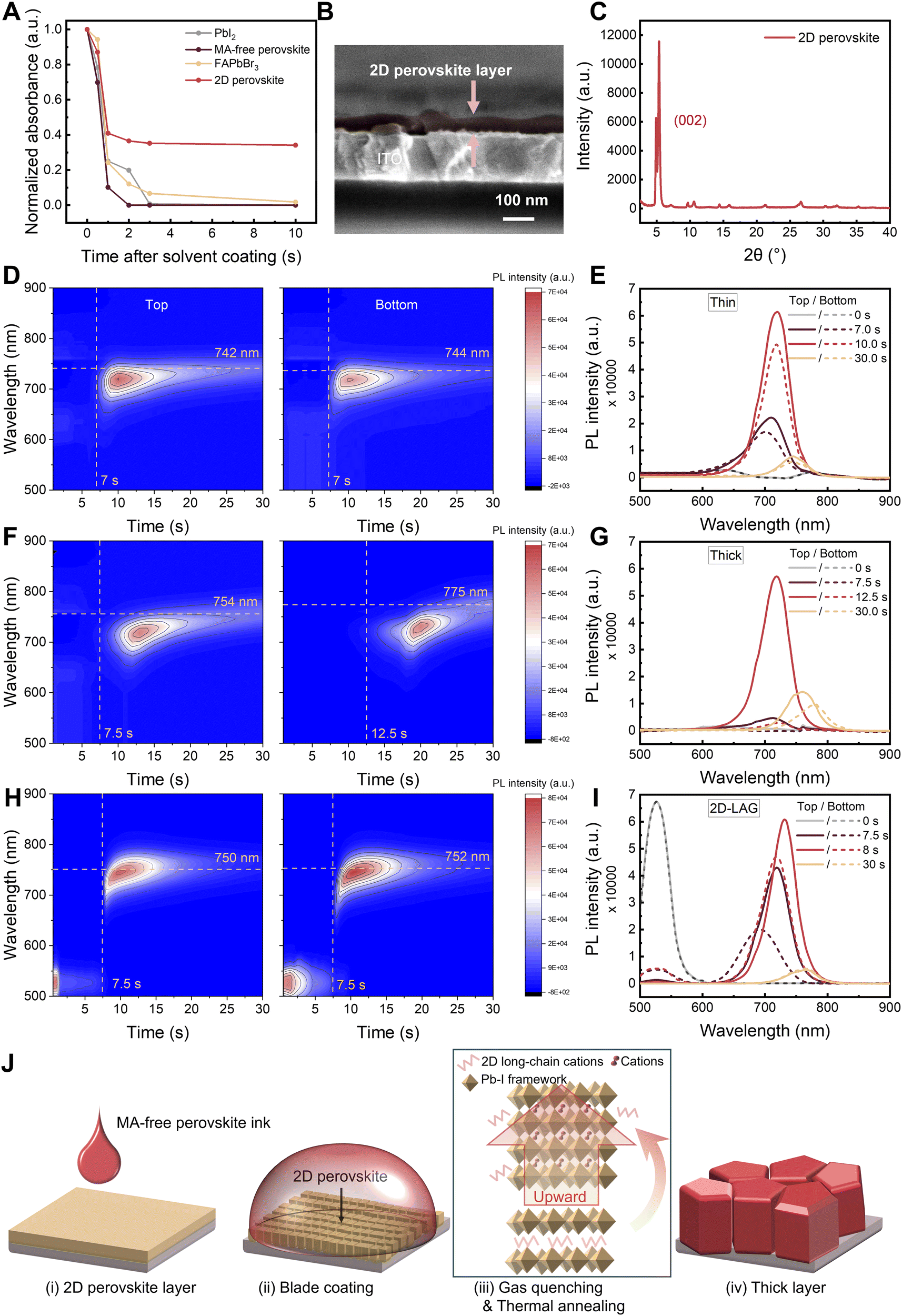 | ||
| Fig. 3 (A) Normalized time-dependent absorbance of the potential seeds after coating the solvents (DMF/NMP) on the top for 10 s: PbI2; MA-free perovskite; FAPbBr3; 2D-perovskite. Corresponding absorbance intensity at 523 nm, 800 nm, 530 nm and 516 nm, respectively. Excitation of halogen lamp from the top with detection on the opposite side. (B) SEM cross-section image and (C) corresponding XRD pattern of a 2D perovskite layer. (D)–(I) In situ monitoring of perovskite film formation by photoluminescence spectroscopy. Time-dependent PL spectra recorded during the gas quenching of blade-coated wet films for (D) a thin film, (F) a thick film and (H) a thick film with 2D PEA2PbI4 perovskite layer-assisted growth. Excitation and detection of PL from the top (bottom) are shown on the left column (right column), respectively, with detection on the same area horizontally in both cases. Corresponding extracted PL spectra at different timescales for (E) a thin film, (G) a thick film and (I) a thick film with 2D PEA2PbI4 perovskite layer, respectively. (J) Schematics of the fabrication process of thick films by using 2D-LAG growth. | ||
These simulations reveal that void formation becomes likely when crystals can nucleate homogenously within a thick wet film. A route to address the problem of void formation is, therefore, to limit or even prevent nucleation. This implies preventing the increase of the precursor concentration beyond the critical threshold φcrit (no supersaturation) during the whole drying process. However, solvent evaporation inevitably leads to an increase of the precursor concentration upon drying. To maintain a low precursor concentration within the liquid film, a balancing sink term must be introduced. The growth of pre-existing crystals, through the uptake of precursor material, is an option of choice for stabilizing the precursor concentration in the remaining liquid film. Ideally, these pre-existing crystals must be positioned in close proximity to the substrate to prevent solvent entrapment beneath them and avoid being dissolved by the surrounding solution that has a low concentration (Extended data Fig. 4). Crystals at the substrate can either be generated using seeds or arise stochastically through heterogeneous nucleation. To enhance the likelihood of heterogeneous nucleation, materials with lower interfacial energy can be introduced at the substrate interface.60
 | ||
| Fig. 4 SEM top-view images (top panel) of perovskite dry films and SEM cross-sectional images (bottom panel) of thin (A), thick (control, B) and thick film with 2D perovskite layer-assisted growth (2D-LAG, C), respectively. All scale bars are 1 μm. (D) UV-vis spectra of the regular one-step blade coated (control) and 2D-LAG perovskite thick films. (E) XRD spectra of the control and 2D-LAG perovskite thick films. (F) XRD different peak intensity of (001) and intensity ratios of (002)/(111) for control and 2D-LAG perovskite films. (G)–(I) Steady-state PL spectra (excited at 405 nm) of perovskite layers on glass substrates: (G) reference thin film (H) control thick film and (I) 2D-LAG thick film. (J)–(L) Corresponding TRPL decay traces (excited at 405 nm). | ||
Independently of the formation mechanisms of these pre-existing perovskite crystals at the substrate, Fig. 2C shows the film formation scenario when they can grow early in the fabrication process, before any further nucleation, and for a fast drying rate. Most importantly, the growth of the pre-existing crystals at the bottom of the film is sufficient to prevent void formation, provided their density is sufficient. However, even if the increase of the precursor concentration in the liquid film is slower than in the scenario without crystals at the substrate (Fig. 2F), the supersaturation regime is still reached. This leads to nucleation and to a similar number of crystals in both scenarios, as shown in Fig. 2G. Therefore, the growth of the pre-existing crystals is not sufficient to stabilize the precursor concentration. Consequently, the process responsible for the increase of the precursor concentration must also be reduced. This can be simply achieved by reducing the drying rate, as confirmed in Fig. 2D. In this case, the drying rate is sufficiently low, the precursor concentration decreases (see Fig. 2F), and no additional crystals nucleate in the wet film (see Fig. 2G). The only remaining active crystallization mechanism is the growth of the pre-existing crystals, which results in an ideal ‘pillar’ morphology.
2.3. Selection of pre-coated layers and impact of layer-assisted growth mechanisms
Having introduced the concept of a bottom layer to prevent void formation, we turn to the selection of materials for the pre-coated layer. It has been reported that microstructured substrates with reduced surface energy promote heterogeneous nucleation and out-of-plane crystal growth.13,61–63 We thus test the coating process of the thick wet film on three different substrates. The optical microscope transmission images, in Fig. S8 (ESI†), reveal that aluminum oxide (Al2O3) and self-assembled monolayer (SAM) exhibit similar behavior as the tin oxide (SnO2) substrate: when the films are coated at a speed exceeding 7 mm s−1, uneven hatched areas appear, indicating the formation of voids at the bottom interface. Although surface energy, substrate morphology, and roughness are known to influence the nucleation and crystallization behavior of perovskite films, our results suggest that these materials with different surface energies and varied surface morphologies appear not to be effective in completely eliminating interfacial voids at the bottom of thick perovskite layers. We further evaluate four potential candidates with structures similar to 3D perovskites, including lead iodide (PbI2), MA-free perovskite, formamidinium lead bromide (FAPbBr3) and a 2D phenyl pethylammonium lead iodide (PEA2PbI4) perovskite. These materials are typically used as nuclei for two-step sequential deposition64–68 and thus provide the seed characteristics employed by the simulations. Especially 2D perovskites have been claimed recently as an excellent choice of seeding the templated growth of 3D perovskite by stabilizing the black phase of formamidinium lead triiodide (FAPbI3).69 A basic requirement for seeding layers is that they remain insoluble, at least for tens of seconds, in the mixed solvent system used for the 3D perovskite coating, thereby maintaining their structural integrity during coating. Therefore, the dissolution of these seeds is studied by following the evolution of their absorbance upon casting a mixture of dimethylformamide/N-methyl-2-pyrrolidone (DMF/NMP) solvents onto these layers as shown in Fig. 3A and Fig. S9 (ESI†). The absorption feature remains unchanged only for the 2D perovskite between 1 s to 10 s, whereas all other materials quickly dissolve in the solvent mix. The solubility of 2D perovskite powder was examined in DMF, NMP, and DMF/NMP mixtures, respectively. Dynamic light scattering (DLS) results (Fig. S10, ESI†) show a gradual decrease in particle size over time in DMF and DMF/NMP mixtures, indicating that the dissolution process is slow enough to make the 2D perovskite layer resilient against redissolution within the targeted time window for the coating of the 3D perovskite layer. Thus, 2D perovskites are suitable candidates for seeding perovskite crystal growth.To experimentally investigate how the 2D perovskite layer alters the crystallization kinetics of the 3D perovskite and how this correlates with a morphological difference, we prepare a pure 2D (PEA)2PbI4 perovskite film of about 25 nm in thickness onto the substrate by blade coating (Fig. 3B). We find that the 2D perovskite film is oriented with the (002) direction parallel to the substrate as evidenced by the most intense diffraction peak positioned at 5.1° and the periodic characteristic (002l) (l = 1–7) at higher angles (Fig. 3C). To investigate the growth of the 3D perovskite layer during the 30-second gas quenching treatment, we utilize in situ photoluminescence (PL) spectroscopy, with excitation from both the top surface and the bottom interface. We plot in Fig. 3D–I the evolution of the PL spectra for a blade-coated thin wet film (Fig. 3D), thick wet film (Fig. 3F) and thick wet film with 2D-perovskite layer (Fig. 3H), respectively. We abbreviate the latter one by 2D-LAG, i.e., 2D perovskite layer-assisted growth. The emergence of PL peaks is interpreted as the initial formation of nanocrystals in the wet film, while the sharp rise of PL intensity is interpreted as evidence for the massive formation of the nanocrystals. Owing to the effect of quantum confinement in the perovskite nanocrystals,38,70,71 the red-shift of the PL peak is assigned to the growth of the individual perovskite nanocrystals.
The evolution of the PL spectra shows a clear distinction of crystallization kinetics: in the thin wet film case (Fig. 3D and E), the first strongest detectible PL peaks are synchronously observed upon excitation from the top and the bottom at about 7 seconds after the start of gas quenching, at a wavelength of 719 nm. The subsequent red shift of these peaks, correlating to the growth of as-nucleated perovskite nanocrystals, does not show a noticeable difference between the top and the bottom excitation. The homogeneous growth kinetics result in the final compact film without voids. In the case of blade-coating a thick film (Fig. 3F and G), the first PL peak emerges at 7.5 seconds when investigated from the top but does not appear until 12.5 seconds when excited from the bottom substrate. The delay aligns well with the results of the PF simulations, which indicate aggregation effects where homogeneous nucleation leads to faster crystalline phase formation at the top surface compared to the bottom surface (Fig. 2B). In more extreme cases, skin effects (Extended data Fig. 2) can occur, both of which contribute to the formation of undesirable bottom voids.
In strong contrast, when coating a thick film with a 2D perovskite layer, the first PL peaks from the top and the bottom are both detected at about 7.5 seconds (Fig. 3H). The subsequent spectral evolutions are clearly more synchronous and show no significant difference between the top and the bottom, suggesting that the perovskite crystallization is less dominant at the liquid–vapor interface when coating a thick film onto a substrate with a 2D perovskite layer. In the case of the 2D-LAG thick film, Fig. 3H, the PL peak at 523 nm that is assigned to 2D perovskite is visible before the beginning of gas quenching and gradually disappears with the emergence of the peaks belonging to 3D perovskite. As shown in Fig. 3I, the simultaneous appearance of 2D and 3D perovskite peaks suggests the formation of quasi-2D perovskite during the transformation process. This is followed by the complete disappearance of the 2D perovskite peak, indicating either a complete transition to 3D perovskite or rapid energy transfer from 2D to 3D perovskite. In this process, the 2D perovskite likely acts as a template for crystal growth and converts into 3D perovskite through cation exchange.68,69,72,73 We further conducted energy dispersive spectroscopy (EDS) elemental line scans to investigate the distribution of elements. As shown in Fig. S11 (ESI†), unlike conventional layered 2D/3D heterostructures, the EDS analysis reveals regions enriched with C at the grain boundaries, which are likely derived from the long-chain cations of the 2D perovskite layer. Fig. 3J summarizes the 2D-LAG strategy, combining our experimental and theoretical findings: the 2D perovskite layer remains undissolved by depositing the MA-free perovskite wet film during blade coating, serving as an initial nucleation site for 3D perovskite. It subsequently enhances the bottom-up crystallization rate of 3D perovskite nanocrystals during drying, ultimately forming a dense and void-free perovskite thick film.
2.4. Impact of void-elimination on thick-film properties
The resulting morphological change of the perovskite films can be seen from the representative cross-sectional and surface SEM images displayed in Fig. 4A–C and the atomic force microscopy images (AFM) presented in Fig. S12 (ESI†), showcasing that 2D-LAG effectively eliminates the bottom voids in thick perovskite layers. As suggested by the PF simulations, upon reduction of the solvent evaporation rate, we can further tune the film morphology from the vertically stacked multiple grains to single grains expanding from the bottom to the top of the film (Fig. S13, ESI†), resulting eventually in over-one-micrometer, monolithic perovskite films (Fig. 4C). Interestingly, opposite to the general trend for perovskite processing, using a moderate drying rate helps to improve morphology. It is highlighted that the introduction of 2D-LAG effectively favors crystallization from the bottom surface, thereby inhibiting the formation of bottom voids, which is consistent with the PF simulations.Having shown the origin of bottom-interface voids in perovskite films with a thickness beyond one-micrometer and the strategy for their elimination, we now turn to the electro-optical characterization of thick perovskite layers without voids. Fig. S14A (ESI†) displays the absorption spectra of layers prepared with different coating speeds. As the film thickness increases, the absorbance increases, but with the appearance of voids, the baseline shifts upward significantly compared to that without voids. The baseline shift ascribed increased light scattering in the presence of the voids at the bottom interface. The XRD spectrum, Fig. S14B (ESI†), reveals that the intensity of the peak at 14° plateaus once the thickness exceeds 600 nm. We focus on the 1100 nm thick film prepared by one-step blade coating (referred to as thick) and prepared with 2D-LAG, unless otherwise specified.
The UV-vis absorption spectrum of a more than one micronmeter thick film of 2D-LAG compared to the control thick film, Fig. 4D, shows an increased absorbance over the whole visible range. The X-ray diffraction (XRD) pattern, Fig. 4E, shows a nearly 4-fold increase of diffraction intensity by the film deposited with 2D-LAG. The improvement of film crystallinity caused by the 2D perovskite layer is also manifested by a noticeable reduction of the full width at half-maximum (FWHM) of the signal assigned to the (001) plane, from 2θ of 0.126° to 0.089°. A detailed analysis of the XRD shows the emergence of texturing along the (001) direction in the 2D-LAG film: as shown in Fig. 4F, this is manifested not only by the intensity increase of the (001) peak, but also by the increase of the intensity ratios between the (002) and the (111) peak. It is noted that no characteristic peaks representing 2D perovskite are found, indicating that the 2D perovskite layer is completely converted into a 3D perovskite layer. To characterize the uniformity between the top surface and bottom interface, we show in Fig. 4G–L both steady-state PL spectra and time-resolved PL (TRPL) decay traces, excited from both sides of the films. When excited from the top and the bottom surfaces, the reference thin film shows slightly different PL intensities in the steady-state PL spectra (Fig. 4G) and PL decay curves (Fig. 4J), which is attributed to the different grain sizes at the top and bottom surfaces. The average PL decay times were extracted by fitting the TRPL decay curves using a bi-exponential function, with the corresponding fitting parameters summarized in Table S1 (ESI†). The control thick film shows a 2-fold higher PL intensity (Fig. 4H) when excited from the top surface, well correlating with a slower PL decay (Fig. 4K). In contrast, the film grown with a 2D perovskite layer shows negligible differences between the PL intensities of the top and bottom interfaces (Fig. 5I) and nearly identical decay kinetics in the transient measurements (Fig. 4L). A comparison of the decay traces of thick perovskite films without and with a 2D perovskite layer indicates significantly slower charge carrier recombination for the latter. These results suggest that the voids formed at the bottom interface not only disrupt film morphology but also cause a reduced perovskite quality with a higher density of electronic trap states causing non-radiative recombination.
 | ||
| Fig. 5 (A) Statistical plot of the PCE for C-PSCs with thick perovskite layers fabricated using the 2D-LAG strategy under varying airflow conditions. (B) Statistical distribution of Jsc of the C-PSCs with 1100 nm thick control and 2D-LAG perovskite layers. (C) Simulated and experimental JV curves of C-PSCs with 1100 nm thick perovskite layers (black: control, red: 2D-LAG, yellow: 2D-LAG with surface passivation by TFMACl). (D) EQE spectra of C-PSCs with around 1100 nm thick control and 2D-LAG perovskite layers. The numbers in the graph represent the respective integrated Jsc values (E). Schematic diagram of PL measurements from the top and bottom surface and spatial distribution of the 25 points of measurement within the 25 cm2 perovskite film. Corresponding PL intensity contour map excited from the top surface and bottom surface of a regular blade-coated thick film (F) and 2D-LAG perovskite film (G). The value inserted is the coefficient variation of PL peak intensity at 25 different positions. (H) Device architecture of fully printed C-PSCs on a flexible or glass substrate. (I) The champion JV curve of fully printed flexible solar cells (J) Reverse scan of JV curve of fully printed mini modules. The inset shows the photograph of a fully printed mini solar module on the rigid substrate. | ||
2.5. Device performance and upscaling the 2D layer-assisted growth film formation
Finally, we turn to investigate the impact of the enhanced microstructure and film quality on photovoltaic performance at the hand of glass/ITO/SnO2/perovskite/PEDOT/Carbon devices (C-PSC), whose cross-sectional SEM images are shown in Fig. S15 (ESI†). All the layers on top of ITO, including the carbon electrode, are fabricated by blade-coating, resulting in the so-called “fully printed” device. When preparing the perovskite layers by conventional one-step doctor blading, progressively increasing perovskite thickness from 250 nm to 1230 nm leads to a significantly enhanced external quantum efficiency (EQE) at higher wavelengths (Fig. S16, ESI†) and thus to an increase in short-circuit current density (Jsc) from 14.53 ± 2.50 to an upper limit of 20.26 ± 3.07 mA cm−2 (Fig. S17, ESI†). However, noticeably lower fill factors (FF) and open-circuit voltages (Voc) are observed for devices limited by void formation at the bottom interface.Guided by processing insights from PF simulations, we first optimize the solvent evaporation rate during gas quenching in the 2D-LAG process by adjusting the airflow rate. As the air flow decrease from 3.0 to 1.0 bar, in Fig. 5A and Fig. S18 (ESI†), the average PCE of C-PSCs increase from 12.9% to 17.0%, accompanied by improvements in Jsc, Voc, and FF, which is in good agreement with the SEM observations (Fig. S13, ESI†). Hereafter, unless otherwise specified, all perovskite films fabricated using the 2D-LAG approach are treated with an airflow of 1.0 bar. In stark contrast, using 2D-LAG in the preparation of an 1100 nm thick perovskite layer not only minimizes the Voc and FF losses (Fig. S19, ESI†) but also significantly improves the average Jsc from 20.86 ± 1.98% to 23.50 ± 1.10% as shown in Fig. 5B. This enhancement is attributed to improved optical absorption and superior interfacial contact enabled by the high-quality thick perovskite film. In Fig. 5C we plot the JV curves of the champion devices: the PCE, Voc, Jsc and FF of the control device are 15.99%, 1.02 V, 22.66 mA cm−2 and 69.16%, respectively. In comparison, the 2D-LAG device yields a PCE of 19.37%, with Jsc = 24.48 mA cm−2, Voc = 1.08 V, and FF = 73.27%. According to the EQE spectra of Fig. 5D, the integrated Jsc of C-PSC prepared with 2D-LAG reaches 23.79 mA cm−2, significantly higher than that of the control thick devices of 19.95 mA cm−2, which is in good agreement with the Jsc from the JV measurement. The solar cell performance is further improved by surface passivation of the perovskite layer with (4-[4-(trifluoromethyl)phenyl]phenyl)methylaminehydrochloride (TFMACl) through a solution immersion treatment, which is compatible with scalable fabrication, resulting mainly in an improvement of Voc from 1.08 V to 1.12 V and a champion PCE of 19.87%, with Jsc = 23.97 mA cm−2 and FF = 74.16%. The main effect of the TFMACl-treatment is found to further reduce non-radiative recombination taking place at the top surface of the perovskite (Fig. S19–S22, ESI†). The reduction of the trap density is further confirmed using an open-source drift-diffusion (DD) package named SIMsalabim,74,75 with which we fit the obtained JV curves by BOAR76 and find out a lower density of trap states in the target device than in the control device (Table S2 and S3, ESI†). We further evaluated the operational stability of the devices, in Fig. S23 (ESI†). The 2D-LAG devices retain 80% of their initial efficiency after 400 hours of continuous operation under 1-sun equivalent illumination at 85 °C, whereas the control thick-film devices exhibit significant degradation, confirming the superior stability imparted by the 2D-LAG strategy.
Lastly, we demonstrate the upscaling of perovskite film deposition by applying the 2D-LAG concept. Prior to the fabrication of solar modules, we examine the film homogeneity by measuring PL intensity at different positions across a film deposited on a 5 × 5 cm2 substrate, a typical size for mini solar modules. In Fig. 5E, a schematic drawing of the measurement protocol is displayed. The resulting contour maps in Fig. 5F and G show the spatial variations of PL intensity measured from both sides of the films. From the contour maps, a coefficient of variation (CV), defined as the ratio of the standard deviation to the mean value, is extracted to quantify the spatial variation of PL intensity. The key observation is an extraordinarily large variation of PL intensity measured from the bottom interface of the thick film deposited without a 2D perovskite layer, whereas such inhomogeneity is remarkably suppressed in the film deposited with 2D-LAG. The results highlight the issue that the void formation at the bottom interface, not easy to discover without inspecting the cross sections of the films, can be a hidden but determining factor causing film inhomogeneity during the upscaling of perovskite film deposition. This is consistent with our previous study and the literature, highlighting that the treatment of the wet film prior to thermal annealing, with either gas flow or antisolvent, most critically determines not only the quality but also the homogeneity of the film.77
We continue to demonstrate the transferability of our approach to flexible substrates, a key milestone to be achieved prior to high-throughput roll-to-roll production, by showing in Fig. 5H and I the architecture and the champion JV curve of printed flexible C-PSCs. The champion flexible C-PSC has an efficiency of 17.53% with Jsc of 22.98 mA cm−2, Voc of 1.09 V and FF of 70.0% obtained from the reverse scan (see also Table 1). It is noticeable that also for flexible C-PSCs the Jsc is higher for 2D-LAG film than for the regular one-step blade coating.
| Methods | J sc (mA cm−2) | V oc (V) | FF (%) | PCE (%) |
|---|---|---|---|---|
| Control | 21.24 | 1.09 | 66.40 | 15.37 |
| 21.35 ± 1.48 | 1.06 ± 0.36 | 60.63 ± 3.20 | 13.80 ± 1.21 | |
| 2D-LAG | 22.98 | 1.09 | 70.00 | 17.53 |
| 22.72 ± 0.71 | 1.09 ± 0.32 | 67.24 ± 2.27 | 16.67 ± 0.79 |
Finally, to highlight the compatibility of the 2D-LAG strategy to upscaling, we fabricate carbon-electrode mini-modules with an aperture area of 20.25 cm−2 on glass substrates, according to the method described in our previous papers.77 The geometric fill factor (GFF) of the champion minimodules is 83.17%. The serial interconnection of the mini-module is realized by P1, P2, and P3 lines. The P1 and P2 lines are patterned by femtosecond laser ablation, whereas the P3 line is fabricated with a tape mask when printing the carbon electrode. The JV curves of mini-module with 7 subcells are displayed in Fig. 5J. The champion modules show an efficiency of 17.38% (Voc = 1.0 V; Jsc = 23.94 mA cm−2, and FF = 73.10% for each subcell). To the best of our knowledge, this work presents one of the highest PCEs for fully printed perovskite mini-modules.78
3. Conclusions
In this work, we focused on printing perovskite layers with more than one micrometer in thickness to meet the upscaling needs of fully printable perovskite PV. We showed that the formation of voids at the bottom interface of perovskite layers is directly correlated to their thickness and represents a key limiting factor for devices with non-reflective carbon electrodes. With the help of PF simulations, we gained comprehensive spatial and temporal insights into the underlying mechanism of void formation at the bottom interface of the perovskite layer: the aggregation of nanograins at the top surface leads to the creation of a closed crystalline layer at the liquid–vapor surface, blocking the evaporation of the remaining solvents. Guided by the results of the PF simulations, we judiciously chose a 2D perovskite layer to accelerate the crystallization rate at the bottom interface, thus homogenizing the crystallinity between the top and bottom of the final film. The PF simulations thus represent a powerful tool for studying the physics of film formation. We emphasize that the combination of experiment and simulation not only deepens our understanding of the mechanism but also provides valuable insights into solving practical challenges to improve film quality. As a result, the current density of fully printed carbon electrode solar cells was significantly increased by obtaining highly crystalline and monolithic perovskite layers of more than one micron. The thick film minimizes photocurrent losses in C-PSCs compared to metal-electrode counterparts, enabling the fabrication of fully printed C-PSCs that achieve record power conversion efficiencies of 19.9% on glass substrates and 17.5% on flexible substrates. Furthermore, the scalability of the 2D-LAG concept was demonstrated by achieving a record 17.4% PCE in a fully printed mini-module. We anticipate that this work will provide crucial insights into the commercialization of fully printed perovskite PVs.Author contributions
S. Q. and H.-J. E. conceived the idea. M. M. and O. R. conceived the idea of using PF simulation prediction. S. Q., H.-J. E., M. M., O. R. and T. D. designed the project. J. H., O. R., T. D., H.-J. E. and C. J. B. supervised the project. M. M. did the PF simulations. S. Q. fabricated the samples and carried out the electrical and optical characterizations. L. D. and N. H. H. helped optimize the flexible solar cells. C. L. deposited the metal electrodes for pin structure devices. S. Q. performed the transfer matrix simulations with assistance from A. D. and K. F. The drift-diffusion simulations were conducted by S. Q. with assistance from J. T. and V. M. L. C. A. B. helped with the SEM characterizations. C. L., J. Z. and F. Y. helped with device optimizations. M. B. deposited the Ag electrode for optical measurement. R. B. helped prepare the mini modules. S. Q. wrote the first draft of the manuscript and M. M. helped with the PF simulation part. A. D., O. R., K. F., J. H., T. D., H.-J. E. and C. J. B. revised the manuscript. All authors contributed to the discussion and commented on the manuscript.Data availability
The data supporting this article have been included as part of the ESI.† Phase-Field Simulation Data for this article, including [Python Scripts, Simulation Data and Figures] are available at [Zenodo] at [URL – https://zenodo.org/records/14967149].Conflicts of interest
There are no conflicts of interest to declare.Acknowledgements
The authors acknowledge financial support from the Bavarian State Government for the Solar Factory of the Future at the Energy Campus Nürnberg (EnCN) (FKZ 20.2-3410.5-4-5). Part of this work has been supported by the Helmholtz Association in the framework of the innovation platform “Solar TAP”. C. J. B. gratefully acknowledges IGK-2495. We further acknowledge financial support from Deutsche Forschungsgemeinschaft (DFG) via the Perovskite SPP2196 programme (Project NO. 506698391). F. Y. acknowledges financial support from Gusu Innovation and Entrepreneurship Leading Talent Program (ZXL2022495). S. Q., C. L., J. T., and J. Z. are grateful for the financial support from the China Scholarship Council (CSC).References
- F. Yang, D. Jang, L. Dong, S. Qiu, A. Distler, N. Li, C. J. Brabec and H.-J. Egelhaaf, Adv. Energy Mater., 2021, 11, 2101973 CrossRef CAS.
- Z. Saki, M. M. Byranvand, N. Taghavinia, M. Kedia and M. Saliba, Energy Environ. Sci., 2021, 14, 5690–5722 RSC.
- H. C. Weerasinghe, N. Macadam, J.-E. Kim, L. J. Sutherland, D. Angmo, L. W. T. Ng, A. D. Scully, F. Glenn, R. Chantler, N. L. Chang, M. Dehghanimadvar, L. Shi, A. W. Y. Ho-Baillie, R. Egan, A. S. R. Chesman, M. Gao, J. J. Jasieniak, T. Hasan and D. Vak, Nat. Commun., 2024, 15, 1656 CrossRef CAS PubMed.
- E. Parvazian and T. Watson, Nat. Commun., 2024, 15, 3983 CrossRef CAS PubMed.
- Y. Han, J. Liu, P. Wang, H. Ma, R. Cai, M. Wang, J. Bian and Y. Shi, ACS Appl. Mater. Interfaces, 2024, 16, 39312–39320 CrossRef CAS.
- H. Zhou, K. Cai, S. Yu, Z. Wang, Z. Xiong, Z. Chu, X. Chu, Q. Jiang and J. You, Nat. Commun., 2024, 15, 6679 CrossRef CAS PubMed.
- B. Ding, Y. Ding, J. Peng, J. Romano-deGea, L. E. K. Frederiksen, H. Kanda, O. A. Syzgantseva, M. A. Syzgantseva, J.-N. Audinot, J. Bour, S. Zhang, T. Wirtz, Z. Fei, P. Dörflinger, N. Shibayama, Y. Niu, S. Hu, S. Zhang, F. F. Tirani, Y. Liu, G.-J. Yang, K. Brooks, L. Hu, S. Kinge, V. Dyakonov, X. Zhang, S. Dai, P. J. Dyson and M. K. Nazeeruddin, Nature, 2024, 628, 299–305 CrossRef CAS.
- F. Jafarzadeh, L. Dong, D. Jang, M. Wagner, G. Koch, S. Qiu, S. Feroze, J. G. Cerrillo, C. J. Brabec, A. D. Carlo and F. Brunetti, Sol. RRL, 2024, 8, 2400530 CrossRef CAS.
- J. Li, J. Dagar, O. Shargaieva, O. Maus, M. Remec, Q. Emery, M. Khenkin, C. Ulbrich, F. Akhundova, J. A. Márquez, T. Unold, M. Fenske, C. Schultz, B. Stegemann, A. A. Ashouri, S. Albrecht, A. T. Esteves, L. Korte, H. Köbler, A. Abate, D. M. Többens, I. Zizak, E. J. W. L. Kratochvil, R. Schlatmann and E. Unger, Adv. Energy Mater., 2023, 13, 2203898 CrossRef CAS.
- Z. Huang, Y. Bai, X. Huang, J. Li, Y. Wu, Y. Chen, K. Li, X. Niu, N. Li, G. Liu, Y. Zhang, H. Zai, Q. Chen, T. Lei, L. Wang and H. Zhou, Nature, 2023, 623, 531–537 CrossRef CAS.
- T. Bu, J. Li, H. Li, C. Tian, J. Su, G. Tong, L. K. Ono, C. Wang, Z. Lin, N. Chai, X.-L. Zhang, J. Chang, J. Lu, J. Zhong, W. Huang, Y. Qi, Y.-B. Cheng and F. Huang, Science, 2021, 372, 1327–1332 CrossRef CAS PubMed.
- M. Jeong, I. W. Choi, E. M. Go, Y. Cho, M. Kim, B. Lee, S. Jeong, Y. Jo, H. W. Choi, J. Lee, J.-H. Bae, S. K. Kwak, D. S. Kim and C. Yang, Science, 2020, 369, 1615–1620 CrossRef CAS PubMed.
- W. Peng, K. Mao, F. Cai, H. Meng, Z. Zhu, T. Li, S. Yuan, Z. Xu, X. Feng, J. Xu, M. D. Mcgehee and J. Xu, Science, 2023, 379, 683–690 CrossRef CAS.
- G. E. Eperon, V. M. Burlakov, P. Docampo, A. Goriely and H. J. Snaith, Adv. Funct. Mater., 2014, 24, 151–157 CrossRef CAS.
- D. Zhao, Y. Yu, C. Wang, W. Liao, N. Shrestha, C. R. Grice, A. J. Cimaroli, L. Guan, R. J. Ellingson, K. Zhu, X. Zhao, R. G. Xiong and Y. Yan, Nat. Energy, 2017, 2, 1–7 Search PubMed.
- Z. Xiao, Q. Dong, C. Bi, Y. Shao, Y. Yuan and J. Huang, Adv. Mater., 2014, 26, 201401685 Search PubMed.
- X. He, J. Chen, X. Ren, L. Zhang, Y. Liu, J. Feng, J. Fang, K. Zhao and S. Liu, Adv. Mater., 2021, 33, 2100770 CrossRef CAS PubMed.
- Y. Deng, E. Peng, Y. Shao, Z. Xiao, Q. Dong and J. Huang, Energy Environ. Sci., 2015, 8, 1544–1550 RSC.
- R. Lin, J. Xu, M. Wei, Y. Wang, Z. Qin, Z. Liu, J. Wu, K. Xiao, B. Chen, S. M. Park, G. Chen, H. R. Atapattu, K. R. Graham, J. Xu, J. Zhu, L. Li, C. Zhang, E. H. Sargent and H. Tan, Nature, 2022, 603, 73–78 CrossRef CAS.
- Z. Chen, B. Turedi, A. Y. Alsalloum, C. Yang, X. Zheng, I. Gereige, A. AlSaggaf, O. F. Mohammed and O. M. Bakr, ACS Energy Lett., 2019, 4, 1258–1259 CrossRef CAS.
- H. Eggers, F. Schackmar, T. Abzieher, Q. Sun, U. Lemmer, Y. Vaynzof, B. S. Richards, G. Hernandez-Sosa and U. W. Paetzold, Adv. Energy Mater., 2020, 10, 1903184 CrossRef CAS.
- Z. Liu, L. Qiu, E. J. Juarez-Perez, Z. Hawash, T. Kim, Y. Jiang, Z. Wu, S. R. Raga, L. K. Ono, S. Liu and Y. Qi, Nat. Commun., 2018, 9, 3880 CrossRef PubMed.
- J. Chen, L. Zuo, Y. Zhang, X. Lian, W. Fu, J. Yan, J. Li, G. Wu, C. Li and H. Chen, Adv. Energy Mater., 2018, 8, 1800438 CrossRef.
- J.-F. Hu, G. Chen, S.-Z. Yu, Y.-X. Lin, K.-Y. Wang, Z.-W. Li, G.-D. Zhang, T.-F. Pan, Y.-J. Li, M.-J. Li, Y.-D. Xia, Y.-F. Lv and Y.-H. Chen, Rare Met., 2024, 43, 1647–1657 CrossRef CAS.
- A. Farag, R. Schmager, P. Fassl, P. Noack, B. Wattenberg, T. Dippell and U. W. Paetzold, ACS Appl. Energy Mater., 2022, 5, 6700–6708 CrossRef CAS.
- A. S. Subbiah, F. H. Isikgor, C. T. Howells, M. De Bastiani, J. Liu, E. Aydin, F. Furlan, T. G. Allen, F. Xu, S. Zhumagali, S. Hoogland, E. H. Sargen, I. McCulloch and S. D. Wolf, ACS Energy Lett., 2020, 5, 3034–3040 CrossRef CAS.
- E. Aydin, J. Liu, E. Ugur, R. Azmi, G. T. Harrison, Y. Hou, B. Chen, S. Zhumagali, M. De Bastiani, M. Wang, W. Raja, T. G. Allen, A. U. Rehman, A. S. Subbiah, M. Babics, A. Babayigit, F. H. Isikgor, K. Wang, E. V. Kerschaver, L. Tsetseris, E. H. Sargent, F. Laquai and S. D. Wolf, Energy Environ. Sci., 2021, 14, 4377–4390 RSC.
- Y. Hou, E. Aydin, M. D. Bastiani, C. Xiao, F. H. Isikgor, D.-J. Xue, B. Chen, H. Chen, B. Bahrami, A. H. Chowdhury, A. Johnston, S.-W. Baek, Z. Huang, M. Wei, Y. Dong, J. Troughton, R. Jalmood, A. J. Mirabelli, T. G. Allen, E. V. Kerschaver, M. I. Saidaminov, D. Baran, Q. Qiao, K. Zhu, S. D. Wolf and E. H. Sargent, Science, 2020, 367, 1135–1140 CrossRef CAS.
- S. Ternes, F. Laufer and U. W. Paetzold, Adv. Sci., 2024, 11, 2308901 CrossRef CAS PubMed.
- V. Negi, O. Wodo, J. J. van Franeker, R. A. J. Janssen and P. A. Bobbert, ACS Appl. Energy Mater., 2018, 1, 725–735 CrossRef CAS.
- O. Wodo and B. Ganapathysubramanian, Comput. Mater. Sci., 2012, 55, 113–126 CrossRef CAS.
- J. J. Michels, K. Zhang, P. Wucher, P. M. Beaujuge, W. Pisula and T. Marszalek, Nat. Mater., 2021, 20, 68–75 CrossRef CAS PubMed.
- O. J. J. Ronsin and J. Harting, Adv. Theory Simul., 2022, 5, 2200286 CrossRef CAS.
- O. J. J. Ronsin and J. Harting, ACS Appl. Mater. Interfaces, 2022, 14, 49785–49800 CrossRef CAS.
- M. Majewski, S. Qiu, O. Ronsin, L. Lüer, V. M. L. Corre, T. Du, C. J. Brabec, H.-J. Egelhaaf and J. Harting, Mater. Horiz., 2025, 12, 555–564 RSC.
- P. Kajal, B. Verma, S. G. R. Vadaga and S. Powar, Global Challenges, 2022, 6, 2100070 CrossRef.
- F. De Rossi, J. A. Baker, D. Beynon, K. E. A. Hooper, S. M. P. Meroni, D. Williams, Z. Wei, A. Yasin, C. Charbonneau, E. H. Jewell and T. M. Watson, Adv. Mater. Technol., 2018, 3, 1800156 CrossRef.
- T. Du, V. Rehm, S. Qiu, S. Pal, D. Jang, Z. Peng, J. Zhang, H. Yuan, J. Briscoe, W. Heiss, C. J. Brabec and H.-J. Egelhaaf, Adv. Sci., 2024, 11, 2401783 CrossRef CAS.
- H. Zhang, K. Song, L. Zhu and Q. Meng, Carbon, 2020, 168, 372–391 CrossRef CAS.
- D. Bogachuk, S. Zouhair, K. Wojciechowski, B. Yang, V. Babu, L. Wagner, B. Xu, J. Lim, S. Mastroianni, H. Pettersson, A. Hagfeldt and A. Hinsch, Energy Environ. Sci., 2020, 13, 3880–3916 RSC.
- K. Domanski, J.-P. Correa-Baena, N. Mine, M. K. Nazeeruddin, A. Abate, M. Saliba, W. Tress, A. Hagfeldt and M. Grätzel, ACS Nano, 2016, 10, 6306–6314 CrossRef CAS.
- T. Du, S. Qiu, X. Zhou, V. M. Le Corre, M. Wu, L. Dong, Z. Peng, Y. Zhao, D. Jang, E. Spiecker, C. J. Brabec and H.-J. Egelhaaf, Joule, 2023, 7, 1920–1937 CrossRef CAS.
- S. Zouhair, C. Clegg, I. Valitova, S. March, J. M. Jailani and V. Pecunia, Sol. RRL, 2024, 8, 2300929 CrossRef CAS.
- K. A. Bush, A. F. Palmstrom, Z. J. Yu, M. Boccard, R. Cheacharoen, J. P. Mailoa, D. P. McMeekin, R. L. Z. Hoye, C. D. Bailie, T. Leijtens, T. Leijtens, I. M. Peters, M. C. Minichetti, N. Rolston, R. Prasanna, S. Sofia, D. Harwood, W. Ma, F. Moghadam, H. J. Snaith, T. Buonassisi, Z. C. Holman, S. F. Bent and M. D. McGehee, Nat. Energy, 2017, 2, 1–7 Search PubMed.
- B. Shi, B. Liu, J. Luo, Y. Li, C. Zheng, X. Yao, L. Fan, J. Liang, Y. Ding, C. Wei, D. Zhang, Y. Zhao and X. Zhang, Sol. Energy Mater. Sol. Cells, 2017, 168, 214–220 CrossRef CAS.
- Y. Jiang, B. Luo, F. Jiang, F. Jiang, C. Fuentes-Hernandez, T. Liu, L. Mao, S. Xiong, Z. Li, T. Wang, B. Kippelen and Y. Zhou, Nano Lett., 2016, 16, 7829–7835 CrossRef CAS PubMed.
- H. Wu, Y. Cheng, J. Ma, J. Zhang, Y. Zhang, Y. Song and S. Peng, Adv. Mater., 2023, 35, 2206574 CrossRef CAS.
- G. F. Burkhard, E. T. Hoke and M. D. McGehee, Adv. Mater., 2010, 22, 3293–3297 CrossRef CAS PubMed.
- R. Kerremans, C. Kaiser, W. Li, N. Zarrabi, P. Meredith and A. Armin, Adv. Opt. Mater., 2020, 8, 2000319 CrossRef CAS.
- F. Gumpert, A. Janßen, C. J. Brabec, H.-J. Egelhaaf, J. Lohbreier and A. Distler, Eng. Appl. Comput. Fluid Mech., 2023, 17, 2242455 Search PubMed.
- S. Chen, X. Xiao, B. Chen, L. L. Kelly, J. Zhao, Y. Lin, M. F. Toney and J. Huang, Sci. Adv., 2021, 7, 26–29 Search PubMed.
- L. R. Zeng, B. Ding, G. Zhang, Y. Liu, X. Zhang, G. J. Yang and B. Chen, Nano Energy, 2024, 122, 109283 CrossRef CAS.
- F. Zhang, J. Song, L. Zhang, F. Niu, Y. Hao, P. Zeng, H. Niu, J. Huang and J. Lian, J. Mater. Chem. A, 2016, 4, 8554–8561 RSC.
- T. Liu, Y. Zong, Y. Zhou, M. Yang, Z. Li, O. S. Game, K. Zhu, R. Zhu, Q. Gong and N. P. Padture, Chem. Mater., 2017, 29, 3246–3250 CrossRef CAS.
- Y. Tu, J. Wu, Z. Lan, X. He, J. Dong, J. Jia, P. Guo, J. Lin, M. Huang and Y. Huang, Sci. Rep., 2017, 7, 44603 CrossRef CAS PubMed.
- H. Hu, D. B. Ritzer, A. Diercks, Y. Li, R. Singh, P. Fassl, Q. Jin, F. Schackmar, U. W. Paetzold and B. A. Nejand, Joule, 2023, 7, 1574–1592 CrossRef CAS.
- H.-Y. Lin, Z. Jiang, S.-C. Liu, Z. Du, S.-E. Hsu, Y.-S. Li, W.-J. Qiu, H. Yang, T. J. Macdonald, M. A. McLachlan and C.-T. Lin, ACS Appl. Mater. Interfaces, 2024, 16, 47763–47772 CrossRef CAS.
- M. Wang, C. Fei, M. A. Uddin and J. Huang, Sci. Adv., 2022, 8, 1–7 Search PubMed.
- S. Chen, X. Dai, S. Xu, H. Jiao, L. Zhao and J. Huang, Science, 2021, 373, 902–907 CrossRef CAS.
- W. A. Dunlap-Shohl, Y. Zhou, N. P. Padture and D. B. Mitzi, Chem. Rev., 2018, 119, 3193–3295 CrossRef.
- J. You, F. Guo, S. Qiu, W. He, C. Wang, X. Liu, W. Xu and Y. Mai, J. Energy Chem., 2019, 38, 192–198 CrossRef.
- X. Duan, X. Li, L. Tan, Z. Huang, J. Yang, G. Liu, Z. Lin and Y. Chen, Adv. Mater., 2020, 32, 2000617 CrossRef CAS PubMed.
- H. Su, Z. Xu, X. He, Y. Yao, X. Zheng, Y. She, Y. Zhu, J. Zhang and S. Liu, Adv. Mater., 2024, 36, 2306724 CrossRef CAS.
- V. Škorjanc, A. Miaskiewicz, M. Roß, S. Maniyarasu, S. Severin, M. R. Leyden, P. Holzhey, F. Ruske, L. Korte and S. Albrecht, ACS Energy Lett., 2024, 9, 5639–5646 CrossRef.
- F. Zhang, C. Xiao, X. Chen, B. W. Larson, S. P. Harvey, J. J. Berry and K. Zhu, Joule, 2019, 3, 1452–1463 CrossRef CAS.
- H. Zhang, Z. Ren, K. Liu, M. Qin, Z. Wu, D. Shen, Y. Zhang, H. T. Chandran, J. Hao, C. Lee, X. Lu, Z. Zheng, J. Huang and G. Li, Adv. Mater., 2022, 34, 2204366 CrossRef CAS.
- Y. Zhao, H. Tan, H. Yuan, Z. Yang, J. Z. Fan, J. Kim, O. Voznyy, X. Gong, L. N. Quan, C. S. Tan, J. Hofkens, D. Yu, Q. Zhao and E. H. Sargent, Nat. Commun., 2018, 9, 1607 CrossRef.
- C. Luo, G. Zheng, F. Gao, X. Wang, Y. Zhao, X. Gao and Q. Zhao, Joule, 2022, 6, 240–257 CrossRef CAS.
- S. Sidhik, I. Metcalf, W. Li, T. Kodalle, C. J. Dolan, M. Khalili, J. Hou, F. Mandani, A. Torma, H. Zhang, R. Garai, J. Persaud, A. Marciel, I. A. M. Puente, G. N. M. Reddy, A. Balvanz, M. A. Alam, C. Katan, E. Tsai, D. Ginger, D. P. Fenning, M. G. Kanatzidis, C. M. Sutter-Fella, J. Even and A. D. Mohite, Science, 2024, 384, 1227–1235 CrossRef CAS PubMed.
- S. Qiu, M. Majewski, L. Dong, D. Jang, V. M. Le Corre, J. G. Cerrillo, O. J. J. Ronsin, F. Yang, F. Guo, K. Zhang, L. Lüer, J. Harting, T. Du, C. J. Brabec and H.-J. Egelhaaf, Adv. Energy Mater., 2024, 14, 2303210 CrossRef CAS.
- H. Yu, H. Wang, J. Zhang, J. Lu, Z. Yuan, W. Xu, L. Hultman, A. A. Bakulin, R. H. Friend, J. Wang, X. K. Liu and F. Gao, Small, 2019, 15, 1804947 CrossRef PubMed.
- Y. Ren, H. Fu, Y. Sun, Z. Li, X. Guo and X. An, Chem. Commun., 2024, 60, 3673–3676 RSC.
- Y. Wang, Z. Shi, Y. Wang, J. Zhang, X. Zhang, X. Li, H. Wang, C. Li, J. Wang, H. Zhang, Y. Yang, J. Zhang, A. Yu and Y. Zhan, Adv. Energy Mater., 2024, 2401721, 1–10 Search PubMed.
- M. Koopmans, V. M. Le Corre and L. J. A. Koster, J. Open Source Softw., 2022, 7, 3727 CrossRef.
- K. Marten, K. Jan Anton, H. Sander and Kostergroup, SIMsalabim Project, https://github.com/kostergroup/SIMsalabim Search PubMed.
- V. M. L. C. Lüer Larry, BOAR: Bayesian Optimization for Automated Research, https://github.com/i-MEET/boar Search PubMed.
- S. Qiu, L. Dong, D. Jang, F. Yang, J. G. Cerrillo, C. Li, Z. Xie, J. Luo, F. Guo, A. Distler, T. Du, C. J. Brabec and H.-J. Egelhaaf, Adv. Energy Mater., 2024, 14, 2402616 CrossRef CAS.
- M. Stefanelli, L. Vesce and A. Di Carlo, Nanomaterials, 2023, 13, 313 CrossRef CAS.
Footnotes |
| † Electronic supplementary information (ESI) available. See DOI: https://doi.org/10.1039/d5ee01722j |
| ‡ These authors contributed equally: Shudi Qiu, Martin Majewski. |
| This journal is © The Royal Society of Chemistry 2025 |