
 Open Access Article
 This Open Access Article is licensed under a
 Creative Commons Attribution 3.0 Unported Licence
Quantifying the rear side contribution in bifacial tandem-photovoltaic devices†
D.
Chojniak
 *a,
M.
Steiner
a,
S. K.
Reichmuth
ab,
A.
Schmid
a,
G.
Siefer
a,
S.
Hooper
c,
D.
Bushnell
c,
D.
Kirk
c,
C.
Case
c and
S. W.
Glunz
ab
*a,
M.
Steiner
a,
S. K.
Reichmuth
ab,
A.
Schmid
a,
G.
Siefer
a,
S.
Hooper
c,
D.
Bushnell
c,
D.
Kirk
c,
C.
Case
c and
S. W.
Glunz
ab
aFraunhofer Institute for Solar Energy Systems ISE, Heidenhofstr. 2, 79110 Freiburg, Germany. E-mail: david.chojniak@ise.fraunhofer.de
bChair for Photovoltaic Energy Conversion, Department of Sustainable Systems Engineering (INATECH), University of Freiburg, Emmy-Noether-Str. 2, 79110 Freiburg, Germany
cOxford PV, Unit 7-8 Oxford Pioneer Park, Mead Rd, Oxford, OX5 1QU, UK
First published on 2nd December 2024
Abstract
Bifaciality is a common approach to increase the power output of photovoltaic devices by capturing a higher portion of the available irradiance. The combination of bifacial and tandem architecture gained significant attention in recent years. However, their accurate characterization remains challenging, hindering device comparisons and the assessment of different development approaches. The procedures for single-junction bifacial devices outlined in IEC TS 60904-1-2 are not fully applicable to two-terminal tandem devices due to current limiting effects. In this study, a combination of simulated and measured data is used to propose new parameters to describe the spectral characteristics of bifacial tandem devices. Those parameters are the short-circuit current and maximum power gain factors σISC and σPMPP as well as the rear side irradiance limit (RIL). Based on these parameters a bifacial perovskite on silicon single-cell module is characterized performing outdoor measurements. Comparing measurements with an open and a covered rear side, a novel approach to quantitatively determine the bifaciality characteristics of bifacial tandem devices is introduced. For the first time, this enables scaling of measured ISC and PMPP values to different rear irradiances. This represents an important step towards a standardized measurement procedure for such devices. Finally, optimization approaches for bifacial tandem devices are proposed based on the presented results.
Broader contextAs the silicon single-junction solar cell technology approaches its efficiency limit, multi-junction solar cells offer enhanced efficiency by combining sub-cells with different bandgaps to use a higher portion of the irradiated energy. Combining the tandem technology with bifaciality further optimizes the irradiance utilization, leveraging ground-reflected light for additional energy generation. Commercially viable tandem devices typically feature 2-terminal designs, posing unique metrological challenges that complicate accurate characterization and therefore comparison with other technologies due to the series connection of the individual sub-cells. In this article we therefore present novel approaches for characterizing bifacial two-terminal tandem devices. The impact of bifaciality for tandem devices under various spectral conditions is investigated through simulations and outdoor measurements on a bifacial perovskite on silicon single-cell module. From these investigations, new parameters are derived to quantify bifaciality effects in tandem devices, facilitating the scaling of measurement results to varying irradiance conditions for the first time. Furthermore, optimization potentials for bifacial tandem devices are presented based on the proposed characterization method. The presented results and procedures mark a crucial step toward standardized measurement methods for bifacial tandem devices and therefore contributes to the development and commercialization of bifacial tandem devices. |
1. Introduction
Silicon single-junction photovoltaic (PV) modules are approaching their theoretical efficiency limit,1 which can be overcome if additional sub-cells are applied forming a multi-junction device. Different material combinations, such as perovskite on silicon (PSC/Si), perovskite on CIGS or III–V on silicon are of particular interest for terrestrial PV applications.2–4Another approach to increase the power output of PV devices is to use the concept of bifaciality.5,6 A bifacial PV device can not only use the irradiance incident from the front but also from the rear side, e.g. reflected from the ground. Therefore, a higher portion of the available irradiance can contribute to charge carrier generation and thus increase its overall power output.
Whereas both approaches are commonly followed individually, there are also applications combining them, resulting in bifacial tandem modules. While the advantages of monolithic bifacial tandem devices, their power generation potential as well as possible optimization approaches have been investigated via simulations by different research groups7–14 measurements on real devices10,15–17 are still rare and so are procedures to accurately determine suitable parameters describing their characteristics.
In the first section of this publication, we discuss theoretical considerations regarding measurement procedures for bifacial devices with respect to IEC TS 60904-1-2.18 After introducing materials and methods, the simulated and measured results of a bifacial PSC/Si single-cell module are presented. Based on the simulated data we suggest new parameters to describe the characteristics of bifacial tandem devices and apply them to an outdoor characterization of the investigated device. In the last section, applications based on the findings of both the simulated and measured data are described. A new approach based on outdoor measurements to quantitatively determine the bifacial current and power contribution for bifacial tandem devices is presented. Finally, approaches are introduced how to consider different outdoor conditions in the optimization of such devices.
2. Theoretical considerations based on IEC TS 60904-1-2
The measurement procedures for the characterization of bifacial PV devices, specified in the technical specification IEC TS 60904-1-2,18 are so far not considering bifacial tandem PV devices. However, such devices require different measurement approaches in several aspects. For two-terminal (2T) devices two major limitations arise, exceeding the procedures used for single-junction PV devices. The first one is that the determination of the rear side characteristics is not possible with single-side illumination. A bifacial single-junction device generates a current and power output according to its quality and characteristics when only illuminated from the rear side. A bifacial tandem device in contrast will be strongly current limited by the top-cell which does not receive photons if the device is only illuminated from the rear side. If the top-cell shows a low shunt resistance a current and power output can be measured, however in this case the measurement does not provide meaningful information about the bifaciality characteristics of the device and will therefore not be considered in this publication. The bifaciality factors for short-circuit current φISC and power output φPmax, used to describe the front and rear side characteristics of single-junction bifacial devices18 are therefore no longer applicable for tandem devices. Both parameters are describing the front to rear side ratio of the respective value when exclusively illuminated from either side with the same intensity as given in eqn (1).‡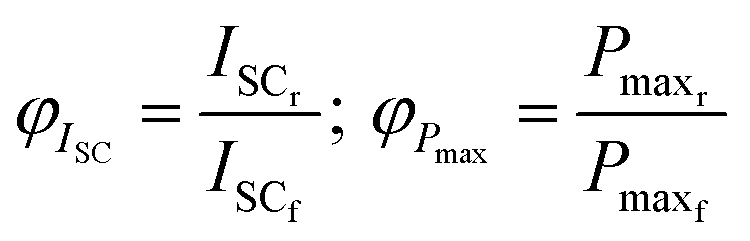 | (1) |
As the top-cell limits the current of a bifacial tandem device if only illuminated from the rear side, both bifaciality factors will always be close to zero. Therefore, we suggest introducing gain factors for both the short-circuit current ISC and maximum power output PMPP. Following the approach of the rear irradiance driven power gain yield, referred to as BiFi in IEC TS 60904-1-2,18 we suggest the following parameters.
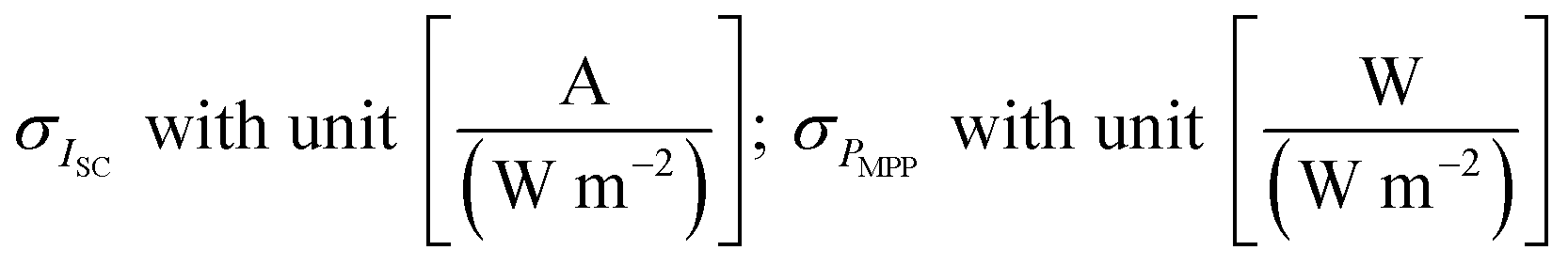 | (2) |
Both parameters describe the bifaciality of the tandem device per portion of rear side irradiance (RSI) while spectral conditions according to the IEC 60904-3 (ref. 19) standard test conditions (STC) are maintained on the modules frontside. The parameters can be calculated according to eqn (3) and (4).
 | (3) |
 | (4) |
Due to current limiting effects the bifaciality factors are strongly influenced by the frontside spectral conditions and can therefore not be considered as constant over a wide range of RSI. To clarify this, we are theoretically observing both possible limitation conditions of a dual junction bifacial tandem device under STC.20
2.1 Scenario 1: top-cell current limitation at STC
If the top-cell limits the device current at STC the RSI, fully absorbed by the bottom-cell which already provides excess current cannot contribute to the overall device current. Therefore σISC, representing the current gain per portion of RSI, equals zero. Thus, the RSI does only contribute to the device's VOC and FF and therefore to its power output. Consequently σPMPP is a function of the gain in VOC and FF during top-cell limiting conditions. However, this contribution is small compared to a direct increase of the device current.2.2 Scenario 2: bottom-cell current limitation at STC
If the bottom-cell is current limiting at STC the RSI incident to a bifacial tandem device can contribute to the overall current and therefore σISC ≥ 0. Such as in Scenario 1 also the device's VOC benefits from the additional irradiance contribution. The FF in contrast decreases due to the increased current of the current limiting bottom-cell, resulting in a decreased current mismatch between both sub-cells.21 The bifacial power gain for bottom-cell limiting conditions σPMPP is therefore driven by changes in ISC, VOC and FF. As a result, σPMPP and σISC for Scenario 1 and 2 differ from each other.At a certain RSI, which is defined by the tandem cell design, the bottom-cell current exceeds the one of the top-cell which will in turn become current limiting and therefore Scenario 2 may shift back into Scenario 1. Consequently, the gain parameters σISC and σPMPP, describing the bifacial characteristics of the device can change and thus cannot be assumed constant for different irradiance conditions. This must be considered if the gain parameters determined at STC are used to extrapolate the power output of the tandem device for different scenarios such as locations or times of a year.
To accurately determine the bifaciality characteristics of 2T bifacial tandem PV devices in indoor measurements, a solar simulator with adjustable spectrum and the ability for simultaneous front and rear side illumination is required. As such measurement equipment is rare, outdoor measurements are used for the characterization of a bifacial tandem device in this publication.
3. Materials and methods
For the simulation and outdoor measurements, a bifacial 2T PSC/Si tandem single-cell module, provided by Oxford PV, was used. A picture of the module, mounted on a dual axis tracker during outdoor measurements, is presented in Fig. 1. The module consists of one M6 (274.15 cm2) PSC/Si tandem solar cell laminated between two 20 cm × 20 cm glass sheets. Four contacts are provided for individual current and voltage probing. The “inactive area” of the module was covered from both sides using black tape to reduce the influence of internal reflections between the glass sheets.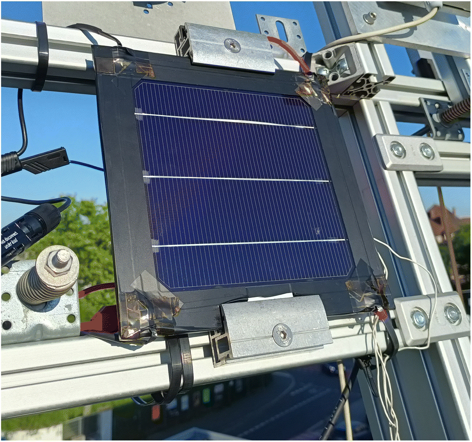 | ||
| Fig. 1 PSC/Si single-cell module mounted on a dual axis tracker at our outdoor measurement setup in Freiburg, Germany, 48.01° N, 7.83° E. | ||
3.1 External quantum efficiency
The module's front and rear side external quantum efficiency (EQE) has been determined using a laser based setup.22,23 The frontside EQE was measured according to the general procedure established for tandem PV devices applying bias light and voltage to measure each sub-cell individually.24,25 To measure the module's rear side EQE the top-cell was light-biased using blue light of high intensity from the frontside to bring the bottom-cell into current limitation. The EQE was then measured using monochromatic light incident to the bottom-cell from the rear side.3.2 Theoretical analysis of outdoor performance
The outdoor simulation is based on the module's front and rear side EQE as well as 9641 outdoor spectra simulated using SMARTS2.26 A broad variation of airmass, aerosol optical depth and precipitable water was applied to cover a wide range of possible spectral conditions (detailed information about the parameter variation can be found in the ESI 7.1†). The RSI was fixed to 80 W m−2§ while the diffuse part of the AM1.5g reference spectrum (AM1.5g(λ) − AM1.5d(λ)) was used as rear side spectrum.To determine the effect of bifaciality on the module's ISC three different measurement conditions have been investigated. The bifacial measurement condition considers the effect and interplay of both sub-cells including the silicon bottom-cell's rear side contribution. For the monofacial measurement condition solely the frontside EQE of the device has been considered. For the top-cell configuration only the current generation of the perovskite top-cell is evaluated, neglecting current limitation by the bottom-cell. Detailed information on the calculation of the respective current shares are provided in the ESI 7.1.†
3.3 Outdoor measurements
For the outdoor measurements the module was mounted on a dual-axis tracker such that the direct portion of the irradiance hits the module perpendicular at each time of the day. Under these conditions the module was exposed to a wide range of spectral conditions, ranging from red-rich in the morning to slightly blue-rich at noon. The measurements have been performed in Freiburg, Germany from the 06th to the 14th of July 2022.To reconstruct the bifacial and monofacial measurement conditions, considered in the simulation, IV measurements have been performed with the module rear side being open and covered. Due to limitations of the measurement setup solely IV sweeps from ISC to VOC have been performed with a sweep time of 10 s. Additional information on the measurement setup as well as the influence of this limitation on the measurement results is discussed in the ESI 7.2.†
3.4 Assessment of outdoor conditions
The total irradiance incident to the module from the front and rear side has been tracked using pyranometers mounted next to the module. A component cell¶ sensor consisting of three single-junction cells with spectrally different absorption bands has been used to monitor the outdoor spectral conditions.27–29 The EQEs of the component cells are shown together with the AM1.5g reference spectrum in the ESI 7.3.† To categorize the outdoor spectral conditions spectral matching ratios (SMR) for all three component cell combinations (SMR12g, SMR13g and SMR23g) are determined using their short-circuit currents measured during outdoor exposure as presented in eqn (5). Based on these values, outdoor spectra can be categorized and evaluated regarding their spectral distribution. However, it is not possible to restore the original spectrum from these three values. A “g” is added to the SMR values, commonly used for concentrator PV applications, to highlight that global spectral conditions are evaluated.29,30 | (5) |
The variables ISCjxMeas correspond to the short-circuit currents measured under outdoor spectral conditions, while ISCjxRef represent the short-circuit currents measured under reference spectral conditions. If all three values equal “one” the actual spectral conditions generate the same current distribution in the sensor as the AM1.5g reference spectrum19 would.30,31 Due to the choice of the component cells' bandgaps, making them sensitive to different ranges of the solar spectrum, the actual spectrum can be assumed to provide a similar spectral irradiance distribution as the AM1.5g reference spectrum itself.27–29 Throughout this publication especially SMR12g will be referred to due to the sensitivity range of the device under test which is mainly covered by sensors number one and two. Therefore, the SMR12g value provides a good indicator for the sub-cell current ratio of the PSC/Si device under test (DUT). This statement as well as the applicability of the utilized component cell sensor for outdoor measurements of PSC/Si tandem devices at the outdoor measurement setup has been investigated and proofed in a previous publication.16 For the indoor characterization of tandem devices usually a parameter Z is used to define the spectral conditions incident to the device, representing the ratio between the actual and the reference effective irradiance incident to a sub-cell.21 For a dual-junction device SMR12g can be rewritten as Z12 according to eqn (6).
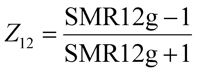 | (6) |
To clearly describe the incident spectral conditions for both, readers familiar with indoor and outdoor characterization methods, both parameters, SMR12g and Z12 will be refereed to. Note that the Z12 values plotted on the upper x-axis are rounded to three decimal places.
3.5 Data processing and filtering
The outdoor dataset has been filtered to exclude unrealistic measurements which may originate from unstable outdoor conditions, malfunction of sensors or inaccurate tracking. A list of all filtering parameters used for the different evaluations can be found in the ESI 7.4.†The measured module parameters ISC and PMPP are divided by the corresponding global normal irradiance (GNI) incident to the module's frontside throughout this publication. This normalization has been applied to show the influence of different spectral conditions on the module's characteristics which would otherwise be hidden within the variation of these parameters with intensity. Due to confidentiality reasons, all datapoints have additionally been normalized by the mean ISC and PMPP determined under reference spectral conditions in the bifacial configuration. To present the data in 2D graphs all values are plotted vs. SMR12g on the lower and Z12 on the upper x-axis, while SMR12g = 1 and Z12 = 0 represent AM1.5g equivalent spectral conditions, SMR12g < 1 and Z12 < 0 can be attributed to red-rich and SMR12g > 1 and Z12 > 0 to blue-rich spectra.21
4. Results and discussion
In this section the results of both, the outdoor simulation and the corresponding outdoor measurement of the single-cell module are presented and discussed.4.1 Outdoor simulation results
Fig. 2 shows the front and rear side EQE of the investigated single-cell module. Due to confidentiality reasons, the presented EQEs are normalized to unity, whereas non-normalized EQEs were used for the simulation. The blue squared and red circular datapoints correspond to the frontside EQE of the perovskite top- and silicon bottom-cell, the black triangular datapoints are showing the rear side EQE of the bottom-cell. While both sub-cells are sharing the frontside irradiance all useable photons incident from the rear side are absorbed by the silicon bottom-cell.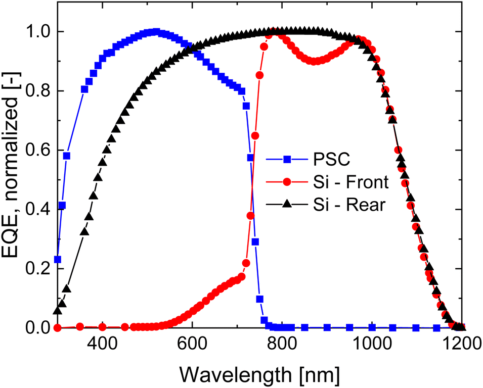 | ||
| Fig. 2 Front and rear side EQEs of a bifacial PSC/Si single-cell module. All three EQEs have been normalized to 1. | ||
The results of the outdoor simulation are presented in Fig. 3. The blue circles are showing the simulation results assuming bifacial measurement conditions (open rear side), while the black triangles correspond to the results if monofacial measurement conditions are applied (covered rear side). The red squared datapoints correspond to the top-cell's ISC per GNI (assuming no current limitation by the silicon bottom-cell). To improve readability the 9641 calculated datapoints have been binned on identical SMR12g values with a step size of 0.001.
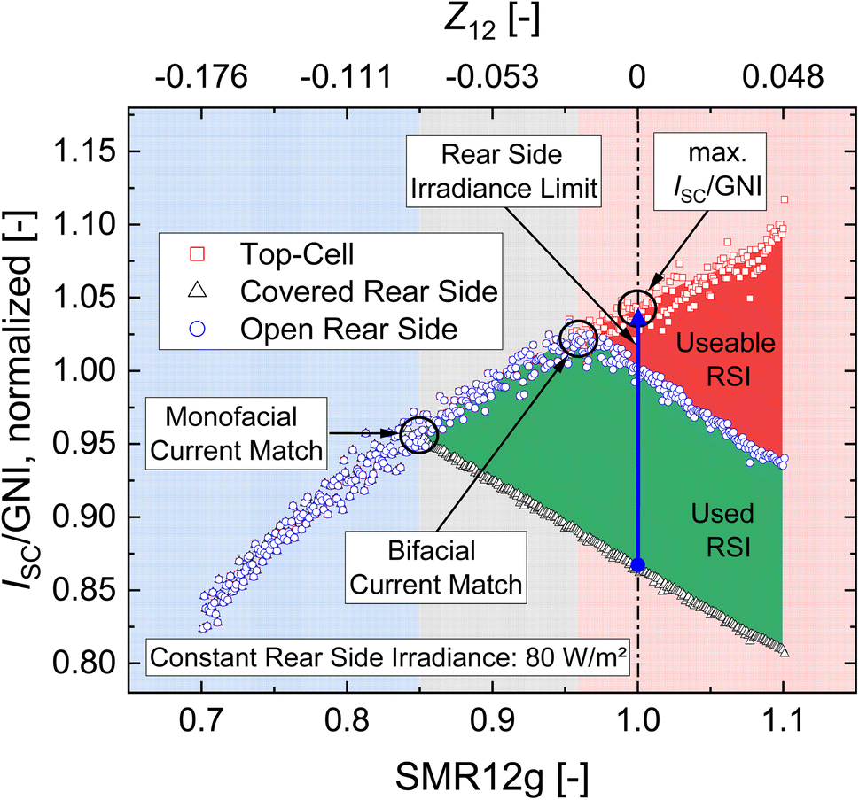 | ||
| Fig. 3 Simulated outdoor measurement based on the front and rear side EQEs shown normalized in Fig. 2 and 9641 outdoor spectra simulated using SMARTS2.26 The results for all three configurations have been binned in SMR12g increments of 0.001 by averaging the results that fall within the respective range. The red squared datapoints have been simulated using the EQE of the top-cell only. The black triangular datapoints are representing an outdoor simulation assuming a monofacial single-cell module, while the blue circular datapoints are representing the outdoor simulation assuming a bifacial configuration. All datapoints have been normalized by the mean ISC/GNI calculated for spectral conditions resulting in SMR12g values between 0.97 and 1.03. The blue, gray and red areas are highlighting spectral ranges in which the bifaciality characteristic of the single-cell module changes due to current limitation effects while the vertical dash-dotted line highlights the reference spectral conditions in this graph (SMR12g = 1 and Z12 = 0). The maximum amount of RSI that can contribute to the device current at reference spectral conditions is represented as blue arrow. | ||
The simulation results are divided into three different areas, highlighted with blue, gray and red backgrounds. The module's characteristics that arise in the different spectral ranges for all three simulation approaches are explained and discussed in the following.
Due to the red-rich spectral distribution, the top-cell, which only receives photons from the frontside, limits the current of the device. Consequently, there is no detectable current contribution of the incident RSI and therefore no difference between the bifacial, monofacial and top-cell simulation results. With increasing SMR12g the portion of high energy photons in the frontside spectrum increases, resulting in higher ISC per GNI values of the current limiting top-cell. Under these spectral conditions σISC = 0 and therefore σPMPP is driven by changes in FF and VOC (compare Scenario 1 in Section 2).
In the monofacial case the silicon bottom-cell becomes current limiting, due to the increasing blue-shift of the frontside spectrum. While the current generation for the monofacial condition solely relies on the frontside spectrum, the module's bifaciality allows for additional charge carrier generation in the bottom-cell, resulting in higher ISC per GNI values. However, the amount of RSI that can contribute to the device current is limited by the difference between the current of the top- and bottom-cell, fully defined by the frontside spectrum. While the frontside spectral distribution becomes more blue-rich the ISC/GNI of the bifacial simulation increases as the ISC/GNI of the top-cell does. Simultaneously, the ISC/GNI of the bottom-cell decreases resulting in a higher portion of RSI that can effectively contribute to the device ISC. The rear side ISC/GNI contribution is highlighted as green area corresponding to the difference between the datapoints resulting from the monofacial and bifacial simulation. Under these spectral conditions the bifacial yield parameters σISC and σPMPP are changing after reaching a certain threshold of RSI, which is again defined by the difference between the top- and bottom-cell's ISC. This situation corresponds to a mixture of Scenario 1 and 2 (Section 2), dependent on the RSI, demonstrating that yield parameters cannot be considered as constant for bifacial tandem devices.
In the bifacial case the available RSI can fully contribute to the device current. Anyhow, there is not enough RSI available to bring the top-cell into current limitation. Therefore, a higher amount of RSI could contribute to the device ISC. The amount of theoretically useable RSI is highlighted with a dark red area between the top-cell only and the bifacial simulation. As the frontside spectrum becomes more blue-rich, the distance between both simulation results increases due to the decreasing irradiance the silicon bottom-cell receives from the frontside. Since the RSI is fixed to a constant value for this simulation the course of the datapoints representing the monofacial and bifacial simulation is parallel in the red area. The distance between both courses is determined by the amount of RSI available. This situation corresponds to Scenario 2 (Section 2) with σISC ≥ 0 and σPMPP being defined by the increase in VOC and ISC as well as a decrease in FF.
4.2 Parameters for bifacial tandem devices
Based on the simulation results different interaction scenarios between front and rear side irradiance, affecting the performance of a bifacial tandem device under varying spectral conditions, have been explained. Following these findings, we are suggesting new parameters for the characterization of bifacial tandem devices.The position of the sub-cells' current match is an important characterization parameter for tandem devices as it typically corresponds to spectral conditions where the maximum tandem cell efficiency is reached.21 For bifacial tandem devices we are expanding this parameter defining a “monofacial current match” and a “bifacial current match”. Both parameters are crucial describing a bifacial tandem device under given spectral conditions, since its bifacial characteristic significantly changes on either side of these points as described before. While the position of the monofacial current match is basically defined by the design of the tandem device, the position of the bifacial current match changes based on the RSI conditions for different albedo, locations or applications. Knowing the position of both parameters and therefore under which conditions a bifacial tandem device operates at STC or any other condition of interest is vital to correctly interpret measurement results. This statement especially holds if results are corrected or extrapolated by scaling irradiance conditions (e.g. for yield simulations).
If scaling of the RSI needs to be applied, e.g. to scale outdoor measurement results to STC, it is crucial to know at which RSI the bifacial characteristic of the device changes. We therefore introduce the RSI limit (RIL), which defines the maximum amount of RSI that can be used by the bottom-cell to contribute to the ISC of the device under a given spectral condition, e.g. AM1.5g reference conditions. In other words, the RIL defines the amount of RSI required to change the sub-cell limitation condition from bottom- to top-cell current limitation and therefore change the bifaciality characteristic of the device.
4.3 Outdoor measurement results
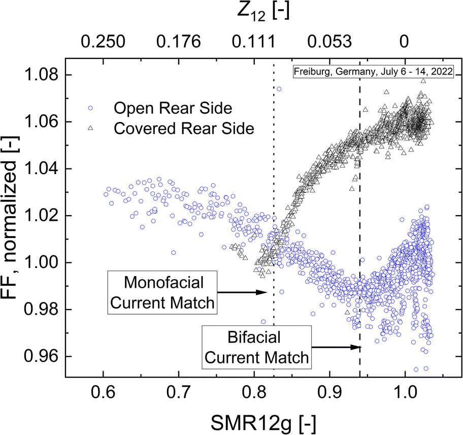
In Fig. 4 the results of the outdoor measurements are shown. In both graphs the blue circular datapoints correspond to measurements with an open, the black triangular datapoints with a covered rear side. The vertical dotted lines represent the spectral position of the monofacial current match and the dashed lines the one of the bifacial current match. Both current matching points have been determined applying linear fits to the respective top- and bottom-cell limiting branches of the datasets.|| The dash-dotted lines highlight SMR12g = 1 and therefore an AM1.5g like current balancing of the single-cell-module's sub-cells with respect to the frontside irradiance.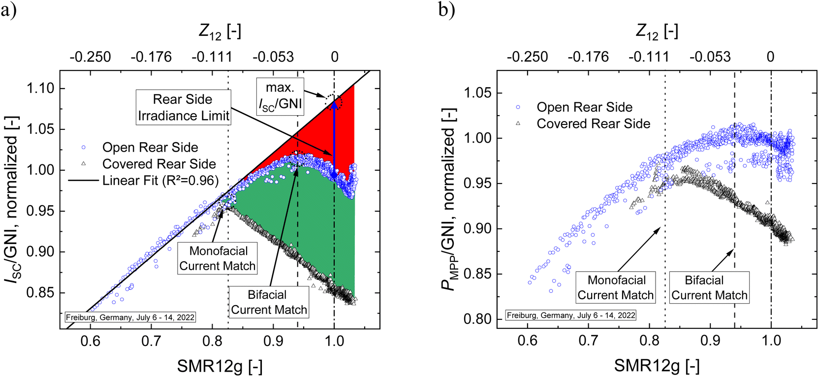 | ||
| Fig. 4 In both graphs blue circular datapoints are representing measurements carried out with an open, black triangular datapoints measurements carried out with a covered rear side. All values are normalized by their respective mean value measured under reference spectral conditions (0.97 < SMR12g, SMR13g, SMR23g < 1.03). The spectral position of the important module parameters, monofacial current match and bifacial current match as well as SMR12g = 1 are highlighted with vertical lines in both graphs. (a) Short-circuit current per global normal irradiance ISC/GNI vs. SMR12g. The green area represents the RSI contributing to the device current while the red area represents the amount of additional RSI which could contribute to the device current under the given spectral conditions. The RIL is graphically represented as blue arrow. (b) Maximum power per GNI (PMPP/GNI). | ||
Comparing the ISC/GNI vs. SMR12g graph shown in Fig. 4a with the simulation results a very good qualitative agreement is found, which enables a clear interpretation of the outdoor measurement data. The module's monofacial current match is reached at SMR12g ∼ 0.83, while the bifacial current match appears at SMR12g values around 0.94. The rather rounded peak of the resulting curve can be explained by the continuous change of the incident RSI under real measurement conditions, which in contrast was kept constant for the simulation. The black solid line represents a linear fit (R2 = 0.96) to the datapoints measured with an open rear side for SMR12g < 0.83 and serves as extrapolation of the top-cell limiting branch of the presented data. At the intersect with the dash-dotted vertical line at SMR12g = 1 the theoretical maximum ISC/GNI of the module under frontside reference spectral conditions can be extracted. This extrapolation is required since, for a two terminal tandem device, it is usually not possible to measure the ISC of the top-cell individually. The green area corresponds to the RSI used under the given spectral conditions, while the red area shows the amount of RSI that could theoretically contribute to the device ISC if it was available. The increase in the module's ISC/GNI at very blue-rich spectral conditions (SMR12g > 1.02) can be explained by increases in the module's temperature** and RSI (plotted together with the GNI in Fig. S3†), both contributing to the ISC of the current limiting silicon bottom-cell.
Fig. 4b shows the module's PMPP/GNI vs. SMR12g. For the monofacial measurement condition the spectral range resulting in the highest PMPP/GNI values is blue shifted compared to the position of the monofacial current match. For an ideal tandem device the spectral conditions of the maximum PMPP/GNI matches the maximum ISC/GNI.21 The deviation can be explained by a strong increase in the module's fill factor FF under silicon limiting conditions, presented in Fig. 5, which overcompensates the drop in current.21 In contrast to the module's ISC/GNI a decrease in PMPP/GNI is visible at very blue rich spectral conditions (SMR12g > 1.02). This can be mainly attributed to the temperature driven decrease in the module's VOC (compare Fig. S4†) as well as a decrease in FF as it can be seen in Fig. 5. This FF reduction results from a decreasing current mismatch between both sub-cells, driven by the described influences of temperature and RSI on the current of the silicon bottom cell, but also by the negative ISC temperature coefficient of the perovskite top-cell.32 Similar observations have been observed and described in detail in ref. 16. Note that the PMPP and FF values under top-cell limiting conditions are underestimated due to hysteresis in the IV curves the plotted datapoints are based on. Additional information regarding this limitation can be found in the ESI 7.2.†
 | ||
| Fig. 5 FF measured with an open (blue circles) and covered (black triangles) module rear side. All datapoints have been normalized to the mean FF measured with an open rear side at reference spectral conditions (max. ±3% deviation of unity for SMR12g, SMR13g and SMR23g). The position of the monofacial and bifacial current match, determined based on the data shown in Fig. 4a, are highlighted as vertical dotted and dashed line. | ||
The FF increase under silicon limiting conditions (SMR12g > 0.94) is less pronounced for the measurements carried out with an open rear side as the module's temperature and RSI increase simultaneously. Both effects contribute to the ISC of the silicon bottom-cell and therefore reduce the current mismatch driven by the blue shift of the frontside spectrum.†† As a result, the highest PMPP/GNI values occur close to the bifacial current match for the measurements carried out with an open rear side.
While the increasing module temperature and RSI result in higher ISC/GNI values at nearly constant frontside spectral conditions (SMR12g ∼1.02) visible in Fig. 4a, the modules PMPP/GNI visible in Fig. 4b decreases. This decrease can be attributed to the decreasing current mismatch between both sub-cells, resulting in decreasing FF values as visible in Fig. 5.16,21
Based on the measurement results, it is obvious that the module is designed for higher rear side intensities as those available at our measurement setup. Since the highest PMPP/GNI values are measured close to the spectral position of the bifacial current match, it would be beneficial to adjust this position to receive the maximum energy yield at a specific location, based on the conditions prevailing there. For the investigated case, where the amount of RSI is not high enough for the actual cell design, this could be achieved by adjusting the sub-cell's current balancing in a way that the silicon bottom-cell receives more photons from the frontside spectrum. This in turn would shift the bifacial current match towards more blue rich spectral conditions. Such optimization potentials drawn from outdoor measurement results are discussed in detail in the following section.
5. Applications
To obtain meaningful results and draw conclusions for the optimization of the investigated device a quantitative characterization of the module's bifaciality characteristics is required. In the following we present an approach to receive such information from the outdoor data presented above and provide optimization guidelines for bifacial tandem devices based on these results. In addition, the introduced characterization approach also enables scaling of measurements to different rear side irradiance levels which is a crucial step towards a standardized measurement procedure for bifacial tandem devices.5.1 Quantitative evaluation of the rear side irradiance contribution
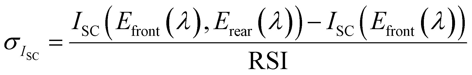
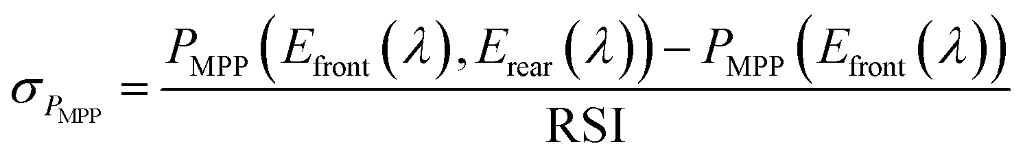
The outdoor measurement results show that the silicon bottom-cell limits the device current under reference spectral conditions, resulting in the situation described as Scenario 2 in the theoretical considerations section. Knowing that in this operation condition the RSI fully contributes to the device ISC, enables the calculation of σISC by comparing the measurements carried out with open and covered rear side. Therefore, the datapoints are filtered according to ref. 29 which includes that SMR12g, SMR13g and SMR23g are within ±3% of unity. A temperature correction was applied to the remaining datapoints to correct their temperature to 41.8 °C, which was found to be the mean operating temperature of the investigated module during reference spectral conditions at our setup with a standard deviation of 1.3 °C. Information about the determination of temperature coefficients can be found in the ESI 7.7.† The modules σISC can then be calculated from the outdoor measurement data presented in Fig. 4a using eqn (7).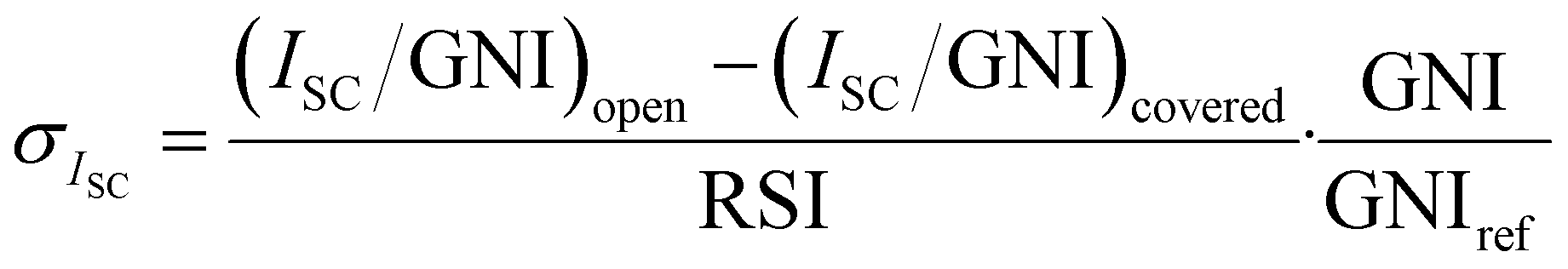 | (7) |
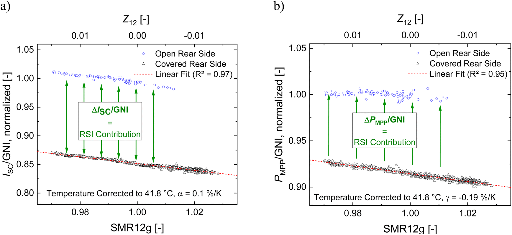 | ||
| Fig. 6 (a) Calculation of the module's σISC based on a comparison of measurements carried out with an open (blue circles) and covered (black triangles) rear side of the module. All datapoints are temperature corrected to 41.8 °C, which was the mean operation temperature (standard deviation: 1.3 °C) of the module at reference spectral conditions. (b) Calculation of the modules σPMPP analogous to the procedure in graph (a). | ||
The resulting σISC can now be used to scale the measured datapoints to different RSI levels. However, a linear scaling can only be applied up to the module's rear side irradiance limit (RIL). Scaling the incident RSI to values exceeding this limit without considering the resulting changes in the module's bifaciality characteristics leads to wrong results. The RIL can be determined based on the measurement carried out under monofacial conditions as well as the extrapolated maximum ISC/GNI presented in Fig. 4. Using eqn (8) a RIL of 135 W m−2 is determined for the investigated module under AM1.5g conditions.
 | (8) |
The same procedure (replacing ISC with PMPP in eqn (7)) can be applied to determine the bifacial contribution to the module's output power as presented in Fig. 6b. Applying this procedure, the module's σPMPP is determined with a standard deviation of 3.6%. As for the ISC, the resulting correlation between RSI and PMPP increase is shown in Fig. S6b.† The higher scatter of the datapoints measured with an open rear side can be attributed to uncertainties in the temperature correction. Knowing both module parameters, σISC and σPMPP, the potential ISC and PMPP of the module assuming different RSI values can be calculated.
By correcting the module's temperature to 25 °C its performance under e.g. bifacial name plate irradiance (BNPI) conditions, requiring a temperature of 25 °C as well as 1000 W m−2 front side irradiance‡‡ and 135 W m−2 RSI can be determined. If the top-cell limits the device current under AM1.5g spectral conditions, gratings or filters can be applied to the measurement setup to party block the incident RSI to bring the bottom-cell into limitation again. The same approach can also be followed if it is required to scale the RSI beyond the RIL. In this case the top-cell will limit the device current and therefore additional RSI will result in an increase in FF and VOC as described for Scenario 1 in Section 2. To determine the resulting effect on the module's PMPP the presented procedure can be applied comparing measurements carried out with and without blocking only a portion of the RSI. In this case the attenuation must be as low that even with the reduced RSI the top-cell still limits the device current.
5.2 Optimization potentials for bifacial tandem solar cell modules
Besides a better understanding of the operation characteristics of bifacial tandem devices the results and conclusions presented in the previous sections can also be used to improve bifacial tandem devices for real world operating conditions. According to Fig. 4b the spectral conditions the investigated module generates the highest ISC/GNI values approximately match the conditions the highest PMPP/GNI values are measured under bifacial measurement conditions. Reaching a high ISC under relevant spectral conditions (usually AM1.5g for terrestrial applications) is therefore a key factor to achieve high power outputs.Fig. 7 shows the module's ISC/GNI plotted as color map vs. SMR12g on the x- and the incident RSI on the y-axis. The black dots represent the maximum amount of RSI which can contribute to the device current under the different spectral conditions. The data is based on the measurement results presented in Fig. 4a as well as a linear fit through the top-cell limiting branch of the open (R2 = 0.96) and bottom-cell limiting branch of the covered (R2 = 0.99) measurement respectively. The σISC determined in the previous section has been utilized to calculate the useable amount of RSI. Even though the graph uses some simplifications it is still valuable to investigate the interplay between RSI, frontside spectral distribution and the resulting ISC/GNI as well as the potential of different optimization approaches for bifacial tandem modules.
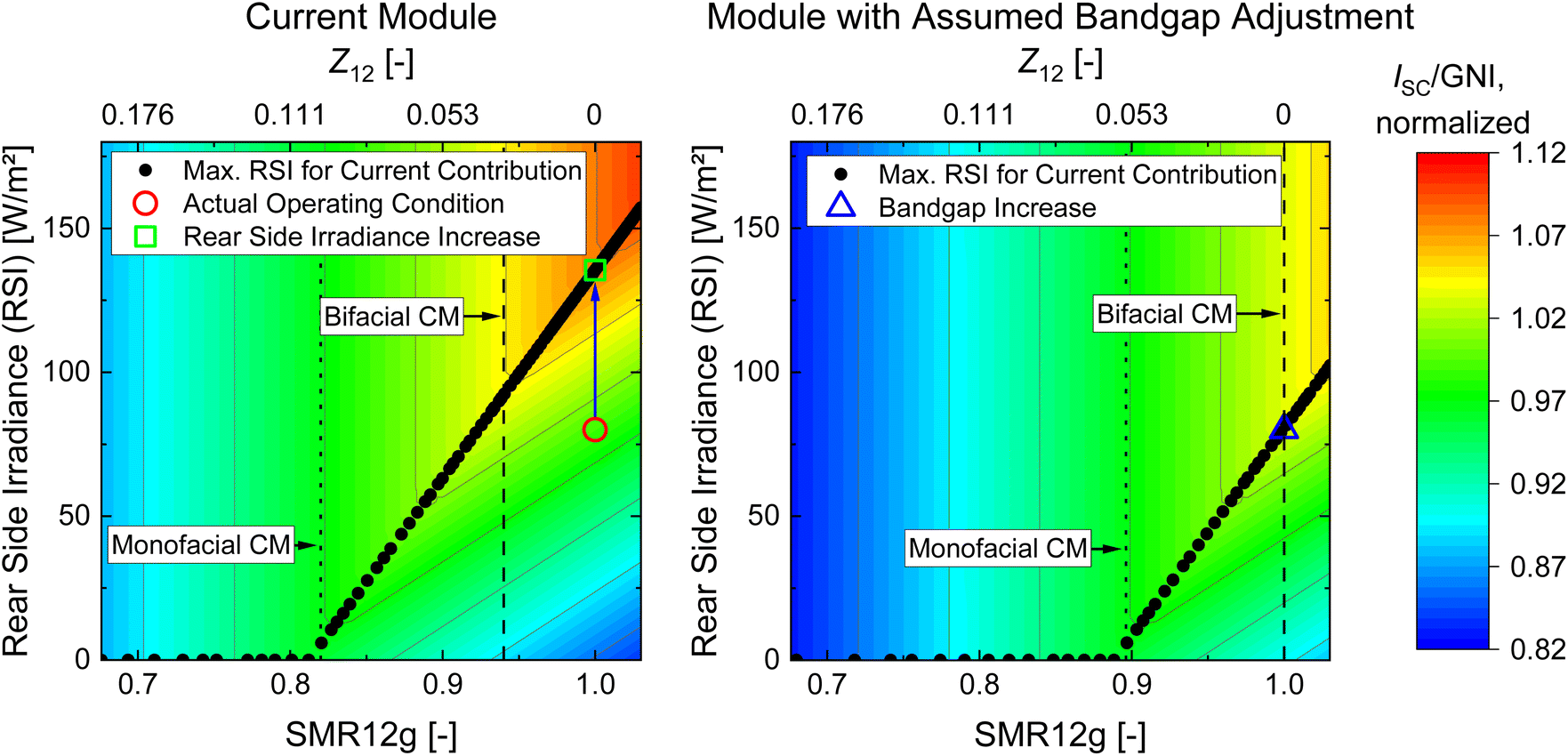 | ||
| Fig. 7 I SC/GNI as a function of RSI (y-axis) and frontside spectral conditions (SMR12g on the lower and Z12 on upper x-axis). The data utilized for the graphs is based on the presented outdoor measurements. The black circular datapoints correspond to the maximum amount of RSI contributing to the current of the investigated module. The vertical dotted and dashed lines represent the positions of the monofacial and bifacial current match. (Left graph) The open red circle represents the position of the actual AM1.5g operating condition. The open green square represents the ideal operating condition that could be reached if a higher amount of RSI would be available. (Right graph) The blue triangle represents the operating conditions that could be reached if the bandgap of the top-cell is increased to achieve a current match of the sub-cells under AM1.5g frontside spectral conditions and an RSI of 80 W m−2. If the bandgap of the top-cell is increased the silicon bottom-cell receives more current from the frontside spectrum. This results in a right shift of the whole color map. | ||
Based on the black datapoints, neglecting temperature effects, the amount of RSI which can directly contribute to the device current is defined by the frontside spectral conditions. The more blue-rich the frontside spectrum the more photons, incident to the rear side, can contribute to the device ISC. While the distribution of the frontside spectral irradiance, respectively SMR12g, is determined by the location the sub-cell's current balancing can be adjusted e.g. by changing the bandgap of the top-cell or making it semi-transparent. Both approaches would result in a different spectral position of the monofacial current match, graphically represented by a shift of the color map in x-direction.
Therefore, the amount of RSI that can contribute to the device current e.g. at AM1.5g spectral conditions (SMR12g = 1) can be changed, adjusting the design of the bifacial tandem device. The potential ISC/GNI increase when adjusting the top-cell's bandgap based on the available RSI as well as the potential of the device if a sufficient RSI is reached can be estimated from the presented graph.
To exemplarily optimize the investigated module to the conditions prevailing at our measurement setup during the investigated period (∼80 W m−2 RSI and close to AM1.5g spectral conditions at noon), the bandgap of the perovskite top-cell needs to be increased such that the silicon bottom-cell receives more photons from the frontside. This adjustment would graphically result in a right shift of the color map while the x-axis remains fixed, as it can be seen in the right graph in Fig. 7. Comparing the actual operating condition (red circle in the left graph) with the ISC/GNI achievable if the top-cell bandgap is adjusted to the available RSI of 80 W m−2 (blue triangle in the right graph), a potential ISC/GNI increase of 4.3% can be estimated. However, if the maximum useable RSI of 135 W m−2 would be available§§ for the investigated device (green square in the left graph) an ISC/GNI increase of 9.3% can be estimated at SMR12g = 1 without adjusting the top-cell's bandgap.
Another approach to optimize a bifacial tandem module and therefore manipulate the presented graph is to improve the EQE of the bottom-cell's rear side. This would decrease the slope of the maximum useable RSI. When improving the rear side EQE of a bifacial tandem device a top-cell with a lower bandgap can be used for a fixed RSI, since less current needs to be generated in the bottom-cell by light impinging on the module's frontside. This in turn would graphically result in a left shift of the color map, and thus potentially enable higher ISC/GNI values (reddish areas in the graph).
Such high ISC/GNI values can also be reached in regions or applications with a high RSI. However, the color map indicates that the proposed improvements always need to be based on a precise investigation of the expected RSI. Considering a sub-cell design with a frontside current balancing strongly shifted towards the top-cell under STC a very high ISC/GNI could be reached with enough RSI. However, if the expected RSI is not reached the device current strongly drops due to the current limitation by the bottom-cell. For the investigated module this effect becomes visible comparing the ISC/GNI values resulting for different amounts of RSI at SMR12g = 1.
Improving the rear side EQE or adjusting the bandgap of a bifacial tandem solar cell's top-cell for applications with a high amount of RSI is especially beneficial for PSC/Si tandem devices since low bandgap perovskite materials tend to be more stable than high bandgap compositions.10,17,33 Therefore, the approaches introduced in this section are supporting the development and commercialization of stable PSC/Si tandem devices which are optimized for bifacial operation.34–36
6. Summary and conclusion
In this publication, we investigated the bifaciality characteristics of bifacial tandem devices utilizing a single cell bifacial PSC/Si tandem module. Through theoretical considerations and a simulation of the module's outdoor performance we described the underlying operation mechanisms, which arise from different sub-cell limitation conditions.While both sides of a bifacial single-junction device can be characterized individually, bifacial tandem devices require simultaneous illumination from the front and rear side to determine their bifaciality characteristics. As such, we propose substituting the bifaciality factors φISC and φPmax used for single-junction bifacial devices with bifacial yield parameters σISC and σPMPP for bifacial tandem devices. These parameters need to be determined under defined frontside spectral conditions (e.g., AM1.5g) and are used to quantify the gain in ISC and PMPP per portion of RSI.
The bifaciality characteristics of a tandem device are not constant but dependent on the actual sub-cell current limitation, which in turn is determined by the incident frontside spectrum, the RSI as well as the device temperature. To address the resulting complexity, we introduced three novel characterization parameters: monofacial current match, bifacial current match, and the rear side irradiance limit (RIL).
Outdoor measurements of the investigated bifacial tandem device with an open and covered rear side demonstrate a good agreement between our simulation results and real-world measurements. Furthermore, the relevance of the newly introduced characterization parameters is revealed by showcasing their applicability to describe the sub-cell current limitation characteristic of the bifacial tandem device under different spectral conditions.
Based on our findings from simulation and outdoor measurements, we presented for the first time a quantitative method to determine the bifacial yield parameters of a tandem module. This in turn enables scaling of measurement results to different RSI conditions, which is a crucial step towards a standardized measurement procedure for bifacial tandem devices which is not available so far.
Building upon the characterization of the bifacial tandem device throughout our work, we finally present different optimization approaches. Our findings underscore the significance of precisely determining the amount of available RSI, which is essential for enhancing the performance of bifacial tandem devices. Specifically, when a perovskite top-cell is incorporated into a tandem device designed for applications with high RSI, adjusting the top-cell's bandgap to match the incident RSI can contribute to produce more stable tandem devices, as a low bandgap top-cell can be used.
In summary, our study provides valuable insights into the bifaciality characteristics of bifacial tandem devices, proposes a quantitative characterization procedure to determine the bifacial current and power gain and presents an approach to determine optimization potentials based on outdoor measurement results.
Data availability
The normalized outdoor measurement raw data used for the evaluations presented in this article, are available at the Open Science Framework using the link: https://osf.io/yjpfx/?view_only=20c90668804e42a0bedcac6d51abbcf5.Author contributions
D. Chojniak: conceptualization, data curation, formal analysis, investigation, methodology, software, visualization, writing – original draft. M. Steiner: conceptualization, data curation, methodology, software, validation, writing – review & editing. S. K. Reichmuth: investigation, methodology, writing – review & editing. A. Schmid: conceptualization, project administration, supervision, validation, writing – review & editing. G. Siefer: conceptualization, project administration, supervision, validation, writing – review & editing. S. Hooper: project administration, resources, writing – review & editing. D. Bushnell: project administration, resources, writing – review & editing. D. Kirk: project administration, resources, writing – review & editing. C. Case: project administration, resources. S. W. Glunz: conceptualization, funding acquisition, project administration, supervision, writing – review & editing.Conflicts of interest
S. Hooper, D. Bushnell, D. Kirk and C. Case are employees at Oxford Photovoltaics Ltd, a company which focuses on developing and commercializing perovskite-based solar technologies. All other authors declare no conflict of interest.Note added after first publication
This article replaces the version published on 2nd December 2024, which contained errors in sections 2 and 6. φPMPP in the original versions has been corrected to φPmax.Acknowledgements
This work was supported by the German Federal Ministry for Economic Affairs and Climate Action (BMWK) under contract number 03EE1087A (KATANA).References
- A. Richter, M. Hermle and S. W. Glunz, Reassessment of the Limiting Efficiency for Crystalline Silicon Solar Cells, IEEE J. Photovolt., 2013, 3(4), 1184–1191, DOI:10.1109/JPHOTOV.2013.2270351.
- M. H. Futscher and B. Ehrler, Modeling the Performance Limitations and Prospects of Perovskite/Si Tandem Solar Cells under Realistic Operating Conditions, ACS Energy Lett., 2017, 2(9), 2089–2095, DOI:10.1021/acsenergylett.7b00596.
- R. A. Hosseinian, A. B. Phillips, K. Ghimire, P. Koirala, Z. Song, H. M. Barudi, A. Habte, M. Sengupta, R. J. Ellingson, Y. Yan, R. W. Collins, N. J. Podraza and M. J. Heben, Irradiance and temperature considerations in the design and deployment of high annual energy yield perovskite/CIGS tandems, Sustain. Energy Fuels, 2019, 3(7), 1841–1851, 10.1039/C9SE00237E.
- P. Schygulla, R. Müller, O. Höhn, M. Schachtner, D. Chojniak, A. Cordaro, S. Tabernig, B. Bläsi, A. Polman, G. Siefer, D. Lackner and F. Dimroth, Wafer-bonded two-terminal III-V//Si triple-junction solar cell with power conversion efficiency of 36.1% at AM1.5g, Prog. Photovolt.: Res. Appl., 2024 DOI:10.1002/pip.3769.
- A. Luque, A. Cuevas and J. M. Ruiz, Double-sided n+-p-n+ solar cell for bifacial concentration, Solar Cells, 1980, 2(2), 151–166, DOI:10.1016/0379-6787(80)90007-1.
- T. S. Liang, M. Pravettoni, C. Deline, J. S. Stein, R. Kopecek, J. P. Singh, W. Luo, Y. Wang, A. G. Aberle and Y. S. Khoo, A review of crystalline silicon bifacial photovoltaic performance characterisation and simulation, Energy Environ. Sci., 2019, 12(1), 116–148, 10.1039/C8EE02184H.
- J. Lehr, M. Langenhorst, R. Schmager, F. Gota, S. Kirner, U. Lemmer, B. S. Richards, C. Case and U. W. Paetzold, Energy yield of bifacial textured perovskite/silicon tandem photovoltaic modules, Sol. Energy Mater. Sol. Cells, 2020, 208, 110367, DOI:10.1016/j.solmat.2019.110367.
- P. Tillmann, K. Jäger, A. Karsenti, L. Kreinin and C. Becker, Model-Chain Validation for Estimating the Energy Yield of Bifacial Perovskite/Silicon Tandem Solar Cells, Sol. RRL, 2022, 6(9), 2200079, DOI:10.1002/solr.202200079.
- J. Chantana, Y. Kawano, T. Nishimura, A. Mavlonov and T. Minemoto, Optimized bandgaps of top and bottom subcells for bifacial two-terminal tandem solar cells under different back irradiances, Sol. Energy, 2021, 220, 163–174, DOI:10.1016/j.solener.2021.03.034.
- M. de Bastiani, A. J. Mirabelli, Y. Hou, F. Gota, E. Aydin, T. G. Allen, J. Troughton, A. S. Subbiah, F. H. Isikgor, J. Liu, L. Xu, B. Chen, E. van Kerschaver, D. Baran, B. Fraboni, M. F. Salvador, U. W. Paetzold, E. H. Sargent and S. de Wolf, Efficient bifacial monolithic perovskite/silicon tandem solar cells via bandgap engineering, Nat. Energy, 2021, 6(2), 167–175, DOI:10.1038/s41560-020-00756-8.
- L. Xu, F. Xu, J. Liu, X. Zhang, A. S. Subbiah and S. de Wolf, Bandgap Optimization for Bifacial Tandem Solar Cells, ACS Energy Lett., 2023, 8(7), 3114–3121, DOI:10.1021/acsenergylett.3c01014.
- Z. Song, C. Li, L. Chen and Y. Yan, Perovskite Solar Cells Go Bifacial-Mutual Benefits for Efficiency and Durability, Adv. Mater., 2022, 34(4), 2106805, DOI:10.1002/adma.202106805.
- K. Jäger, P. Tillmann, E. A. Katz and C. Becker, Perovskite/Silicon Tandem Solar Cells: Effect of Luminescent Coupling and Bifaciality, Sol. RRL, 2021, 5(3) DOI:10.1002/solr.202000628.
- J. Tang, J. Xue, H. Xu, Y. Li, S. Lin, B. Li, D. Zhong, G. Li, Y. Jiang and Q. Chen, Power generation density boost of bifacial tandem solar cells revealed by high throughput optoelectrical modelling, Energy Environ. Sci., 2024, 17(16), 6068–6078, 10.1039/d4ee01173b.
- M. de Bastiani, E. van Kerschaver, Q. Jeangros, A. Ur Rehman, E. Aydin, F. H. Isikgor, A. J. Mirabelli, M. Babics, J. Liu, S. Zhumagali, E. Ugur, G. T. Harrison, T. G. Allen, B. Chen, Y. Hou, S. Shikin, E. H. Sargent, C. Ballif, M. Salvador and S. de Wolf, Toward Stable Monolithic Perovskite/Silicon Tandem Photovoltaics: A Six-Month Outdoor Performance Study in a Hot and Humid Climate, ACS Energy Lett., 2021, 6(8), 2944–2951, DOI:10.1021/acsenergylett.1c01018.
- D. Chojniak, M. Steiner, S. K. Reichmuth, T. Rößler, A. Schmid, G. Siefer and S. W. Glunz, Outdoor measurements of a full-size bifacial Pero/Si tandem module under different spectral conditions, Prog. Photovolt.: Res. Appl., 2023, 32(4), 219–231, DOI:10.1002/pip.3753.
- E. Ugur, E. Aydin, M. de Bastiani, G. T. Harrison, B. K. Yildirim, S. Teale, B. Chen, J. Liu, M. Wang, A. Seitkhan, M. Babics, A. S. Subbiah, A. A. Said, R. Azmi, A. Rehman, T. G. Allen, P. Schulz, E. H. Sargent, F. Laquai and S. de Wolf, Front-contact passivation through 2D/3D perovskite heterojunctions enables efficient bifacial perovskite/silicon tandem solar cells, Matter, 2023, 6(9), 2919–2934, DOI:10.1016/j.matt.2023.05.028.
- International Electrotechnical Commission, Photovoltaic Devices Part 1-2: Measurement of Current-Voltage Characteristics of Bifacial Photovoltaic (PV) Devices, 1st edn, (IEC TS 60904-1-2:2019), 2019 Search PubMed.
- International Electrotechnical Commission, Photovoltaic Devices: Part 3: Measurement Principles for Terrestrial Photovoltaic (PV) Solar Devices with Reference Spectral Irradiance Data, 4th edn, (IEC 60904-3:2019), 2019 Search PubMed.
- International Electrotechnical Commission, Photovoltaic Devices Part 1: Measurement of Photovoltaic Current-Voltage Characteristics, 3rd edn, (IEC 60904-1:2020), 2020 Search PubMed.
- M. Meusel, R. Adelhelm, F. Dimroth, A. W. Bett and W. Warta, Spectral mismatch correction and spectrometric characterization of monolithic III-V multi-junction solar cells, Prog. Photovolt.: Res. Appl., 2002, 10(4), 243–255, DOI:10.1002/pip.407.
- M. Mundus, D. Lill, J. Hohl-Ebinger and W. Warta, Advanced Spectral Response Measurement with Wide Range Tunable Laser System, 29th European Photovoltaic Solar Energy Conference and Exhibition, 2014, pp. 3439–3442, DOI:10.4229/EUPVSEC20142014-5DV.3.49.
- M. Mundus, Ultrashort Laser Pulses for Electrical Characterization of Solar Cells, PhD thesis, University of Konstanz, 2016.
- J. Burdick and T. Glatfelter, Spectral response and I–V measurements of tandem amorphous-silicon alloy solar cells, Solar Cells, 1986, 18(3–4), 301–314, DOI:10.1016/0379-6787(86)90129-8.
- M. Meusel, C. Baur, G. Létay, A. W. Bett, W. Warta and E. Fernandez, Spectral response measurements of monolithic GaInP/Ga(In)As/Ge triple-junction solar cells: Measurement artifacts and their explanation, Prog. Photovolt.: Res. Appl., 2003, 11(8), 499–514, DOI:10.1002/pip.514.
- C. Gueymard, SMARTS2, A Simple Model of the Atmospheric Radiative Transfer of Sunshine: Algorithms and Performance Assessment, Solar Energy Center, University of Central Florida, 1995 Search PubMed.
- G. Peharz, G. Siefer, K. Araki and A. W. Bett, Spectrometric outdoor characterization of CPV modules using isotype monitor cells, in Proceedings of the 33rd IEEE Photovoltaic Specialists Conference, IEEE, San Diego, CA, USA, 2008, pp. 1–5 Search PubMed.
- J. Jaus, T. Mißbach, S. P. Philipps, G. Siefer and A. W. Bett, Spectral Measurements Using Component Cells: Examinations On Measurement Precision, in Proceedings of the 26th European Photovoltaic Solar Energy Conference, WIP, Hamburg, Germany, 2011, pp. 176–182 Search PubMed.
- M. Steiner and G. Siefer, Translation of outdoor tandem PV module I–V measurements to a STC power rating, Prog. Photovolt.: Res. Appl., 2023, 31(8), 862–869, DOI:10.1002/pip.3691.
- C. Domínguez, I. Antón, G. Sala and S. Askins, Current-matching estimation for multijunction cells within a CPV module by means of component cells, Prog. Photovolt.: Res. Appl., 2013, 21(7), 1478–1488, DOI:10.1002/pip.2227.
- R. Núñez, C. Domínguez, S. Askins, M. Victoria, R. Herrero, I. Antón and G. Sala, Determination of spectral variations by means of component cells useful for CPV rating and design, Prog. Photovolt.: Res. Appl., 2016, 24(5), 663–679, DOI:10.1002/pip.2715.
- E. Aydin, T. G. Allen, M. de Bastiani, L. Xu, J. Ávila, M. Salvador, E. van Kerschaver and S. de Wolf, Interplay between temperature and bandgap energies on the outdoor performance of perovskite/silicon tandem solar cells, Nat. Energy, 2020, 5(11), 851–859, DOI:10.1038/s41560-020-00687-4.
- M. de Bastiani, A. S. Subbiah, M. Babics, E. Ugur, L. Xu, J. Liu, T. G. Allen, E. Aydin and S. de Wolf, Bifacial perovskite/silicon tandem solar cells, Joule, 2022, 6(7), 1431–1445, DOI:10.1016/j.joule.2022.05.014.
- D. Chojniak, M. Schachtner, S. K. Reichmuth, A. J. Bett, M. Rauer, J. Hohl-Ebinger, A. Schmid, G. Siefer and S. W. Glunz, A precise method for the spectral adjustment of LED and multi-light source solar simulators, Prog. Photovolt.: Res. Appl., 2024, 32(6), 372–389, DOI:10.1002/pip.3776.
- C. Stark and M. Theristis, The impact of atmospheric parameters on the spectral performance of multiple photovoltaic technologies, in 2015 IEEE 42nd Photovoltaic Specialist Conference (PVSC), IEEE, 2015, pp. 1–5 Search PubMed.
- International Electrotechnical Commission, Photovoltaic Concentrators (CPV): Performance Testing – Part 3: Performance Measurements and Power Rating, 1st edn, (IEC 62670-3:2017), 2017 Search PubMed.
Footnotes |
| † Electronic supplementary information (ESI) available. See DOI: https://doi.org/10.1039/d4el00027g |
| ‡ For both situations STC (1000 W m−2 AM1.5g, 25 °C) should be met. |
| § Which is the approximate rear side irradiance available at our outdoor measurement setup at AM1.5g spectral conditions during the period in which outdoor measurements have been carried out for this work. |
| ¶ A component cell is a single-junction solar cell with identical optical properties as the multi-junction cell it is based on. To do this, the complete multi-junction stack is created with only one active pn-junction. |
| || Fit ranges for the determination of the monofacial current match: SMR12g = 0.77 to SMR12g = 0.82 (top-cell limiting, R2 = 0.94) and SMR12g = 0.84 to SMR12g = 1.03 (bottom-cell limiting, R2 = 0.99). Fit ranges for the determination of the bifacial current match: SMR12g = 0.6 to SMR12g = 0.9 (top-cell limiting, R2 = 0.98) and SMR12g = 0.97 to SMR12g = 1.02 (bottom-cell limiting, R2 = 0.82). |
| ** An increasing module temperature leads to a narrowing of the bandgap of the silicon bottom-cell and thus to an increase in its current. In addition, the silicon bottom-cell does also not lose current in the short-wavelength range due to the negative ISC temperature coefficient of the perovskite top-cell.32 |
| †† For the measurements carried out with a covered rear side the monofacial current match is reached at significantly lower SMR12g values and therefore earlier in the morning and later in the afternoon. During those times of the day the incident frontside spectrum changes faster16 and therefore the change in the module's temperature is, compared to noon, lower in relation to the change in frontside spectral conditions. Additionally, the RSI does not influence the bottom-cell's current under monofacial measurement conditions. Therefore, the compensation of the spectrally induced mismatch, visible under bifacial measurement conditions, is less pronounced for the measurement under monofacial conditions, resulting in a steeper increase in the module's FF. |
| ‡‡ With AM1.5g spectral conditions. |
| §§ This could be achieved, for example, by adapting the installation conditions. |
| This journal is © The Royal Society of Chemistry 2025 |