
 Open Access Article
 This Open Access Article is licensed under a
 Creative Commons Attribution 3.0 Unported Licence
Industrialization of perovskite solar cell fabrication: strategies to achieve high-throughput vapor deposition processes†
Julian
Petry
 *a,
Viktor
Škorjanc
b,
Alexander
Diercks
c,
Thomas
Feeney
c,
Amedeo
Morsa
d,
Sara Rose
Kimmig
ef,
Jens
Baumann
g,
Frank
Löffler
g,
Stefan
Auschill
h,
Joshua
Damm
a,
Daniel
Baumann
a,
Felix
Laufer
c,
Jona
Kurpiers
b,
Michael
Müller
d,
Lars
Korte
b,
Steve
Albrecht
bi,
Marcel
Roß
*b,
Ulrich W.
Paetzold
*ac and
Paul
Fassl
*ac
*a,
Viktor
Škorjanc
b,
Alexander
Diercks
c,
Thomas
Feeney
c,
Amedeo
Morsa
d,
Sara Rose
Kimmig
ef,
Jens
Baumann
g,
Frank
Löffler
g,
Stefan
Auschill
h,
Joshua
Damm
a,
Daniel
Baumann
a,
Felix
Laufer
c,
Jona
Kurpiers
b,
Michael
Müller
d,
Lars
Korte
b,
Steve
Albrecht
bi,
Marcel
Roß
*b,
Ulrich W.
Paetzold
*ac and
Paul
Fassl
*ac
aInstitute of Microstructure Technology (IMT), Karlsruhe Institute of Technology (KIT), Hermann-von-Helmholtz-Platz 1, 76344 Eggenstein-Leopoldshafen, Germany. E-mail: julian.petry@kit.edu; paul.fassl@kit.edu; ulrich.paetzold@kit.edu
bSolar Energy Division, Helmholtz-Zentrum Berlin (HZB), Kekuléstraße 5, 12489 Berlin, Germany. E-mail: marcel.ross@helmholtz-berlin.de
cLight Technology Institute (LTI), Karlsruhe Institute of Technology (KIT), Engesserstraße 13, 76131 Karlsruhe, Germany
dInstitute of Energy Materials and Devices (IMD-1), Forschungszentrum Jülich GmbH, Wilhelm-Johnen-Straße, 52428 Jülich, Germany
eInstitute of Applied Geosciences (AGW) Geochemistry and Economic Geology, Karlsruhe Institute of Technology (KIT), Adenauerring 20b, 76131 Karlsruhe, Germany
fInstitute of Applied Geosciences (AGW) Laboratory for Environmental and Raw Materials Analysis, Karlsruhe Institute of Technology (KIT), Adenauerring 20b, 76131 Karlsruhe, Germany
gVon Ardenne GmbH, Am Hahnweg 8, 01328 Dresden, Germany
hM.Braun Inertgas-Systeme GmbH Vacuum Deposition & Sublimation Dresden, Niedersedlitzerstraße 75, 01257 Dresden, Germany
iFaculty IV – Electrical Engineering and Computer Sciences, Technical University Berlin, 10587 Berlin, Germany
First published on 14th May 2025
Abstract
Vapor phase deposition processes hold great potential for industrializing the deposition of perovskite-based absorbers, offering a pathway to commercialization. Specifically, the scalability, ability to produce conformal coatings, and established use in industrial processing of optoelectronic devices lead to the assumption that thermal sublimation is inherently suitable for commercial-scale perovskite solar cell production. However, ensuring economic viability requires a detailed assessment of achievable production throughputs, a key factor in achieving cost-effective large-scale manufacturing. This work bridges the gap between research focus and industry needs by introducing and analyzing three strategies to increase production throughput in an industrial context: (1) we investigate the thermal stability of key perovskite precursor materials to provide guidelines for safe operation by mitigating decomposition risks. (2) We critically evaluate the industrial feasibility of common deposition modes, including co-deposition and sequential deposition, as scaling from laboratory to industrial production introduces new challenges in terms of material utilization and compositional material homogeneity. In addition, we analyze the static deposition rate profiles of key perovskite precursor materials and use this data to conceptualize a linear sublimation source. (3) A simulation-based approach allows an estimation of the horizontal scale-out required to achieve a production throughput of 1000 M10-size wafers per hour, which is considered the minimum threshold for pilot-scale production. This analysis explores strategies to achieve a fabrication throughput that is three orders of magnitude higher than the current academic discussion of accelerated vapor phase deposition based on laboratory-scale equipment. The sublimation of the organic precursor material is identified as a critical bottleneck and alternative deposition methods for achieving high production throughput are discussed. By addressing these key technical and economic challenges, our study offers practical insights for the transition of sublimation-based perovskite deposition from laboratory research to industrial-scale manufacturing.
Broader contextMetal halide perovskite-based solar cells have evolved from a research innovation to a commercially viable technology, achieving market entry in 2024. Their high power conversion efficiencies and cost-effectiveness position them as a prime candidate for next-generation photovoltaics, complementing established silicon in tandem devices. However, transitioning to large-scale deployment requires industrial manufacturing processes that meet scalability and economic demands. Vapor phase deposition is a promising method for perovskite fabrication due to its uniform and conformal coating properties and its widespread use in thin-film industry. Despite these advantages, current laboratory-scale vapor-based processes are limited by low deposition rates, creating a significant barrier to achieving the production throughput necessary for industrial adoption. The present study addresses the critical challenges of scaling vapor-based processes by evaluating the thermal stability of perovskite precursors, analyzing deposition modes, and conceptualizing a linear sublimation source for production throughput analysis. Practical guidelines are offered to support the transition from research-scale methods to scalable and cost-effective manufacturing, thereby accelerating the commercialization of perovskite-based photovoltaic technologies. |
Introduction
The rapid development of perovskite solar cells (PSCs) marks an unprecedented advance in photovoltaic (PV) technology. Impressive progress has been made in the efficiency and stability of single-junction PSCs, achieving a certified record power conversion efficiency (PCE) of 26.95%.1 Monolithically interconnected perovskite/silicon (PVSK/Si) tandem solar cells are of particular interest as they make more efficient use of the solar energy spectrum. Consequently, they are able to significantly increase the effective device PCE beyond what either technology could achieve on its own. LONGi Solar has recently reported a laboratory-scale record efficiency of 34.6% for PVSK/Si tandem solar cells and further demonstrated PCEs of 30.1% on commercial M6-size wafers.2,3 OxfordPV in collaboration with Fraunhofer ISE, has demonstrated a full-scale PVSK/Si module with an area of 1.68 m2 and a module efficiency of 26.9%, surpassing the efficiency of conventional Si-based modules for the first time.4 These achievements are setting a remarkable benchmark for this technology that far exceeds the efficiency of established Si PV, and underscores the potential of hybrid lead halide perovskites as perfect partners for Si-based solar cells.Current research on PSCs predominantly uses solution-based perovskite absorber layer deposition, accounting for more than 98% of peer-reviewed research articles.5 This disproportionate focus on solution processes can be attributed to two primary factors: lower equipment costs and the ability to rapidly iterate the material composition and solar cell architecture. In contrast, perovskite deposition via vapor phase deposition is severely underrepresented in recent academic literature despite being superior to solution-based processes in terms of achieving uniform and conformal coverage over large areas, as well as on textured Si substrates.6 Achieving full coverage over pyramidal structures of Si wafers via solution processes typically requires the deposition of a thick perovskite layer, resulting in thickness variations across the thin film, or the use of tailored surface textures with pyramid sizes below 1 μm.7–10 A recent industry survey conducted by Abzieher et al. found that approximately 40% of companies engaged in perovskite-based PV research reported activities related to vapor-based processes.11 This highlights a significant discrepancy between laboratory-scale innovations and commercially viable technologies. The key requirements for commercialization are: (i) uniform, conformal, and reproducible deposition of perovskite absorber layers at high throughput, (ii) high material utilization and production yield, and (iii) compatibility with industrially relevant textured silicon wafers. Examples of successful and scalable thin-film manufacturing can be found in the established thin film industry (e.g., CdTe or copper indium gallium selenide (CIGS) PV, and organic light-emitting diodes (OLED)), which is exclusively based on vapor-based techniques.12–15
The potential of thermally sublimed perovskites to fabricate highly efficient single-junction PSCs as well as their integration into tandem architectures has been demonstrated by several research groups. We note that many scientific publications are using the terms “evaporation” and “sublimation” interchangeably. We will refer to the processes as sublimation, as in the processes discussed here, there is no formation of a liquid phase from which the material evaporates. Important milestones for co-deposited perovskite absorbers have been achieved: long-term stable PSCs with PCEs exceeding 20% have been reported by Roß et al.16 These devices demonstrated stable performance for over 1000 hours in the p–i–n configuration. Gil-Escrig et al. were the first to demonstrate a conformal coating on microscopically textured substrates, achieving a PCE of 15%.17 Ritzer et al. developed the first all-evaporated perovskite solar module utilizing a co-deposited absorber layer reaching a PCE of 16.6% for an aperture area of 51 cm2 with low upscaling losses.18 Recent studies have focused on sequential deposition of the respective perovskite precursors, achieving PCEs of 24.4% and 17.8% in the n–i–p and p–i–n architecture for a methylammonium (MA)-free perovskite composition, respectively.19,20 More recently, Zhou et al. utilized sublimed MACl as an additive for sequentially deposited PSCs in the n–i–p architecture achieving a certified PCE of 26.4%, representing the record efficiency at that time.21 Despite the advantages in coating quality and process integration, thermal sublimation of perovskite absorbers is described in the literature to face limitations in deposition rate, which impacts the production throughput.22,23 Recently, there has been a growing interest in increasing the deposition speed of vacuum-deposited perovskite absorbers with efforts of Piot et al. investigating the effects of increased deposition rates for co-deposited MAPbI3-based PSCs.24 In this study, a 1 μm-thick absorber was deposited in 50 min with PCEs comparable to the slower baseline process exceeding 19%. Similar results were obtained in a study of Dewi et al., with deposition times of co-deposited MAPbI3 thin films of 600 nm thickness being reduced from 150 min to 25 min without compromising device performance.25 However, when looking at the achieved deposition rates, it is evident that they are still far too low for industrially relevant production throughputs.11
The transition from research-to pilot production and ultimately to industrial-scale production at the GWp-level presents significant challenges.26,27 For context: continuous operation of a pilot line at a production throughput of 1000 M10-size wafers per hour would consume up to 8.76 million wafers per year, equivalent to a production capacity of ∼73 MWp/a at 25% cell efficiency. Based on the current certified efficiency record of 34.6% for laboratory-scale PVSK/Si tandem solar cells,3 the production capacity could be increased by ∼38%rel compared to the silicon single-junction reference, equivalent to a production capacity of ∼101 MWp/a. These potential capacity increases are a primary motivation for research into PVSK/Si tandem solar cells. Numerous studies have claimed the self-evident applicability of vapor-based techniques for perovskite deposition to industrial processes, as it is a mature technology that has demonstrated conformal and uniform deposition properties for large areas.6,18,28,29 However, few studies have addressed the complexities of implementing these processes at industrially relevant throughputs in a cost-effective manner.
In this work, we aim to fill this knowledge gap by analyzing the potential of different scaling strategies to increase the production throughput. Such strategies can be divided into two categories: vertical scale-up and horizontal scale-out. In this context, vertical scale-up refers to maximizing production throughput by increasing the deposition rates of individual sublimation sources and improving process effectiveness. This approach is constrained by intrinsic factors such as the thermal stability of the materials. Horizontal scale-out involves increasing production throughput by adding additional equipment, such as more or larger sublimation sources. While effective, this approach requires significant capital investment, which affects the economic viability of the technology. First, the potential of vertical scale-up is investigated by analyzing the thermal stability and sublimation characteristics of key perovskite precursor materials, formamidinium iodide (FAI) and lead iodide (PbI2). Second, commonly used deposition modes are discussed in the context of a linear source setup with a focus on process effectiveness and material utilization. Third, the deposition rate of a conceptual linear source is estimated based on experimentally available data using laboratory-scale point sources. This calculation aims to determine the necessary horizontal scale-out to achieve the minimum threshold production throughput of 1000 M10-size wafers per hour. Such insights are essential to advance perovskite-based solar cells from promising laboratory research to economically viable large-scale applications.
Results and discussion
This work investigates the potential for increasing the production throughput of perovskite absorber deposition by introducing and assessing three strategies: (1) elevate the source temperature to increase the deposition rate. This approach is intrinsically limited by the thermal stability of the materials. We aim to provide guidelines for a safe sublimation temperature range without the risk of decomposition. (2) Improve process effectiveness through optimized source layout. We discuss common deposition modes such as co-deposition and sequential deposition in context of industrial linear sources. Strategy (1) and (2) are categorized as vertical scale-up strategies. (3) Addition of multiple sources in series to increase production throughput. We estimate the required horizontal scale-out to achieve a pilot line production of 1000 M10-size wafers per hour (Fig. 1). | ||
| Fig. 1 Comparison of laboratory- and pilot-scale production. Laboratory-scale production predominantly uses co-deposition of all precursors, with material mixing achieved by positioning the sublimation sources off-center relative to the substrate. Pilot-scale production uses moving wafer carriers that pass perpendicularly through the array of industrial point or linear sublimation sources. | ||
Strategy 1: maximize deposition rates by elevating sublimation source temperature
This section explores if the perovskite deposition rate can be increased beyond commonly used values by elevating the sublimation temperature, a strong lever for increasing the overall production throughput without requiring significant investment. Addressing potential limitations on the achievable deposition rate and production throughput requires a thorough understanding of the thermal stability of perovskite precursors under sublimation conditions. The most critical materials in this context are PbI2, cesium iodide (CsI), FAI and methylammonium iodide (MAI), as they contribute most to the overall perovskite composition.30 With regard to its sublimation characteristic, each component presents unique challenges, potentially limiting the production throughput. In this study, each material is sublimed at stepwise increasing temperatures, and the deposited material is analyzed to track changes in its composition and to identify potential decomposition products. In addition, the evolving gas phase under sublimation conditions is studied to provide insights into the reactions taking place at elevated temperatures.Thermal stability of organic perovskite precursor materials
Controlled and reproducible sublimation of organic perovskite materials is known to be notoriously difficult.25,31–36 The sublimation characteristics of MAI are described as omnidirectional and cloud-like.37 Consequently, controlling the deposition rate of MAI using conventional quartz crystal microbalance (QCM) measurements is non-trivial.36 Strategies to improve process control include tracking the background pressure caused by MAI sublimation or positioning a QCM to detect PbI2 and MAI deposition simultaneously, effectively measuring the rate of MAPbI3 deposition.35 At low temperatures, the dissociation of MAI to methylamine and hydroiodic acid (HI) dominates the sublimation dynamics. The sticking of MAI to the QCM is influenced by its material purity, which can fluctuate due to variations in material synthesis, further complicating the reproducible deposition control.31,33–35 Several reports on the effect of MAI purity indicate that phosphorus-based impurities have a significant effect on its sublimation characteristics, the most common are methylammonium hypophosphite (MAH2PO2) and methylammonium phosphonate (MAH2PO3). Thermal cracking of MAI has been observed at temperatures above 170 °C, resulting in the formation of methyl iodide and ammonia.38,39The relatively lower intrinsic thermal stability of MA-based perovskite absorbers motivated the search for FA-based perovskite compositions.40,41 While recent literature has pivoted to focus on FA-based perovskite compositions, analysis of FAI decomposition under sublimation conditions remains limited. A recent study presented by Kroll et al. shows that thermal cracking of FAI occurs at temperatures above 200 °C, with fragmentation into 1,3,5-triazine, ammonia and hydrogen cyanide.32 Critically, there is no experimental evidence that the cracking products are incorporated into the perovskite lattice.42
We investigate the thermal stability of FAI and MAI using a Duran tube sublimation setup. Samples are collected from three harvesting zones: material in the crucible residue, the main fraction and volatiles deposited under active cooling (see schematic in Fig. 2A; the respective fractions are indicated by the superscript of B–D). The analysis of the thermal stability of MAI is elaborated in the ESI† with 1H, 13C and 31P nuclear magnetic resonance (NMR) spectra shown in Fig. S1.† Interestingly, no evidence of MAI decomposition is observed, even at a temperature of 240 °C, the highest temperature used in this experiment under vacuum conditions. Phosphorous-containing compounds are detectable in the volatiles deposited under active cooling, which could be identified as MAH2PO2 with characteristic signals at 6.22 ppm and 7.83 ppm found in the 1H-NMR spectra.33 A red-colored material accumulated in the crucible residue upon heating, the identity of which remains elusive. Optical photographies of collected materials are depicted in Fig. S2.†
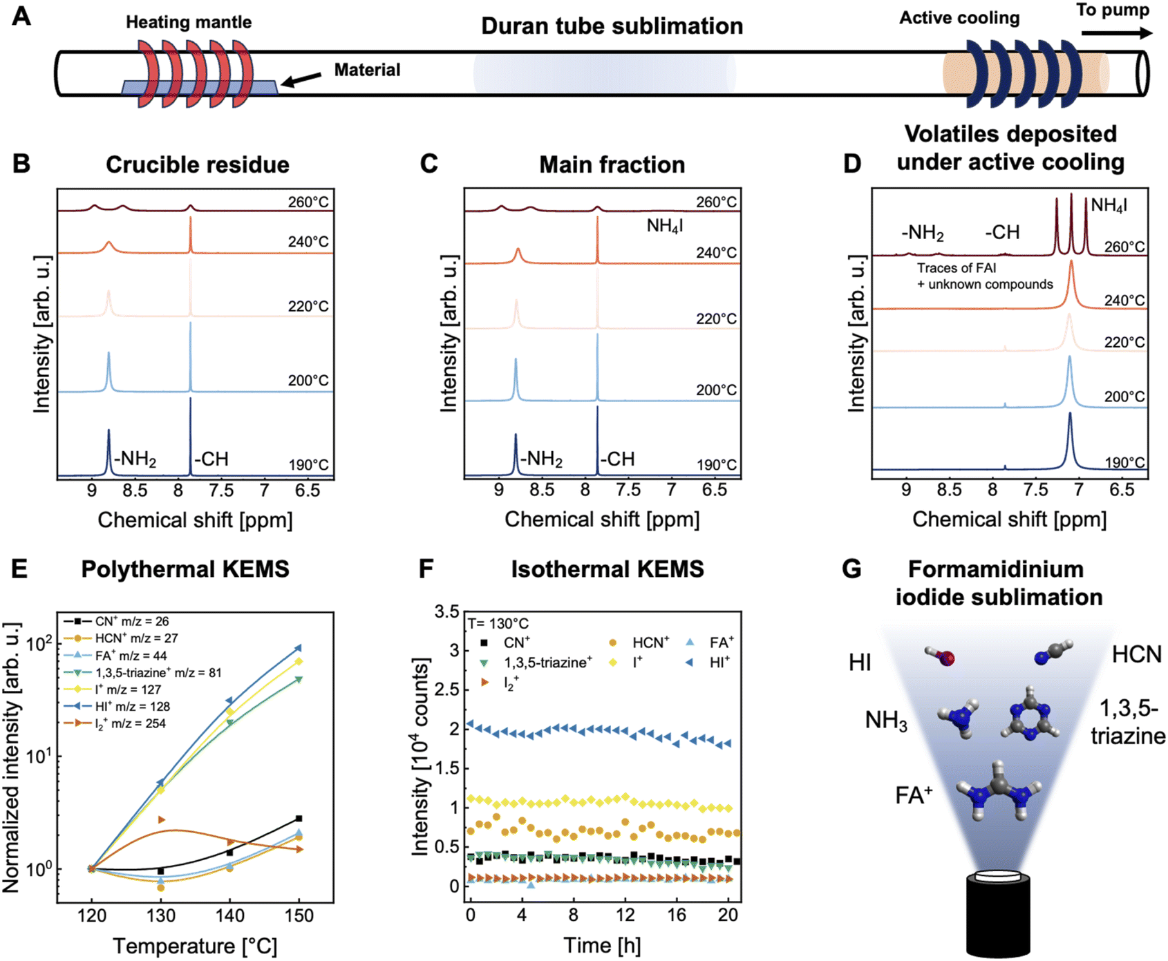 | ||
| Fig. 2 Investigation of the thermal stability of FAI under sublimation conditions. (A) Schematic drawing of the employed sublimation setup used. Material is collected from the crucible residue, main fraction, and the volatiles deposited under active cooling. (B–D) 1H-NMR spectra of collected material for increasing sublimation temperatures (E) KEMS measurements of pristine FAI with increasing temperature. Lines are guides for the eye. (F) Isothermal KEMS measurements at 130 °C. (G) Graphical summary of species emitted from the sublimation source. | ||
The analysis of the thermal stability of FAI reveals more drastic changes. A progressive discoloration from off-white to yellow and finally to gray/black is observed for the crucible residue, indicating material decomposition and coke formation at temperatures above 240 °C. Optical photographs of the collected samples are depicted in Fig. S3.† This suggests that FAI undergoes significant chemical transformation at elevated temperatures, affecting both appearance and composition. To identify potential decomposition products and impurities, all samples collected are analyzed by 1H-NMR spectroscopy (Fig. 2B–D). Samples exposed to temperatures exceeding 240 °C exhibit broadening of the characteristic amidine NMR peak at 8.80 ppm, with additional peak splitting occurring at 260 °C. This behaviour is not fully understood but has previously been attributed to the presence of Lewis acids.43 We hypothesize an increased amount of HI in the sample due to the dissociation reaction of FAI. The main fraction shows a yellow discoloration above 240 °C and peak splitting of the amidine signal at 8.80 ppm is observed. A small additional peak at 7.09 ppm, consistent with ammonium iodide (NH4I), points to decomposition processes generating ammonia and HI through dissociation and thermal cracking of FAI, respectively. The detection of NH4I is critical because it implies that this decomposition product could deposit on the substrate, potentially affecting perovskite formation. However, we note that the substrate temperature is commonly around room temperature and thus no deposition of NH4I is expected under operational conditions. A reference 1H-NMR spectrum of NH4I is provided in Fig. S4.† No further impurities are detected for sublimation temperatures below 240 °C. Volatiles deposited under active cooling show discoloration for temperatures above 240 °C. Interestingly, NH4I is detected at all temperatures. Traces of FAI are detected above 240 °C, which we attribute to the material transfer distance being increased with temperature. No sign of a 1,3,5-triazine signal is detected by 1H-NMR spectroscopy which is attributed to its volatile nature with the external cooling being insufficient for the material to deposit.
Further analysis of the molecular identity of emitted species from a point source was conducted by Knudsen effusion mass spectrometry (KEMS) measurements at increasing temperatures (Fig. 2E and F). By analyzing the material flux emitted by a point source with mass spectrometry, conclusions can be drawn about the species present. Thermodynamic equilibrium within the point source is achieved by using a “semi-closed” system with a small orifice. Thereby, only a small amount of material is effused at a time, reducing the disturbance of the equilibrium conditions. Eight different ions, which can be either ionized gas molecules or their fragments, could be identified for FAI![[thin space (1/6-em)]](https://www.rsc.org/images/entities/char_2009.gif) :NH3+ (m/z = 17), CN+ (m/z = 26), HCN+ (m/z = 27), FA+ (m/z = 44), 1,3,5-triazine+ (m/z = 81), I+ (m/z = 127), HI+ (m/z = 128) and I2+ (m/z = 254) (Fig. S5A†). The m/z value for NH4+ is equal to that of water and, therefore, cannot be deconvoluted or interpreted further. All presented measurements are qualitative and the intensities of different ions do not necessarily correlate with the relative abundance of the corresponding gas species. However, when comparing the evolution of temperature-dependent measured counts of observed ions, correlations between different species can be found. For example, the abundance of HI+, I+ and 1,3,5-triazine+ appear to be correlated. Furthermore, FA+ and CN+/HCN+ correlate with a minimum abundance at 130 °C, after which the intensity increases again and are anticorrelated to the intensity of I2+ ions. Interestingly, the generation channels for FA+ and HCN+ belong to the dissociation and thermal cracking process, respectively. This indicates that the gas phase reactions of FAI have a more complex underlying reaction process with unknown reaction pathways explaining the observed correlation of FA+ and CN+. Further elucidation of respective decomposition mechanisms is required to better understand the gas phase chemistry of FAI, which is beyond the scope of this work. The presented polythermal measurements describe a snapshot of emitted species at the given temperature. However, a week-long campaign duration is desirable for industrialization. To gain more insights, the temporal change of emitted species was tracked by isothermal KEMS measurements at a constant temperature of 130 °C. The intensities of all observed ions stabilized and remained constant within measurement accuracy. After around 20 h, ∼95% of the material was consumed (Fig. 2F). A second isothermal KEMS measurement at 150 °C showed fast material depletion after ∼5 h (Fig. S5B†). A graphical summary of observed species is depicted in Fig. 2G.
:NH3+ (m/z = 17), CN+ (m/z = 26), HCN+ (m/z = 27), FA+ (m/z = 44), 1,3,5-triazine+ (m/z = 81), I+ (m/z = 127), HI+ (m/z = 128) and I2+ (m/z = 254) (Fig. S5A†). The m/z value for NH4+ is equal to that of water and, therefore, cannot be deconvoluted or interpreted further. All presented measurements are qualitative and the intensities of different ions do not necessarily correlate with the relative abundance of the corresponding gas species. However, when comparing the evolution of temperature-dependent measured counts of observed ions, correlations between different species can be found. For example, the abundance of HI+, I+ and 1,3,5-triazine+ appear to be correlated. Furthermore, FA+ and CN+/HCN+ correlate with a minimum abundance at 130 °C, after which the intensity increases again and are anticorrelated to the intensity of I2+ ions. Interestingly, the generation channels for FA+ and HCN+ belong to the dissociation and thermal cracking process, respectively. This indicates that the gas phase reactions of FAI have a more complex underlying reaction process with unknown reaction pathways explaining the observed correlation of FA+ and CN+. Further elucidation of respective decomposition mechanisms is required to better understand the gas phase chemistry of FAI, which is beyond the scope of this work. The presented polythermal measurements describe a snapshot of emitted species at the given temperature. However, a week-long campaign duration is desirable for industrialization. To gain more insights, the temporal change of emitted species was tracked by isothermal KEMS measurements at a constant temperature of 130 °C. The intensities of all observed ions stabilized and remained constant within measurement accuracy. After around 20 h, ∼95% of the material was consumed (Fig. 2F). A second isothermal KEMS measurement at 150 °C showed fast material depletion after ∼5 h (Fig. S5B†). A graphical summary of observed species is depicted in Fig. 2G.
In summary, the FAI sublimation temperature should not exceed the range of 220–240 °C, above which significant decomposition, with coke formation within the crucible residue is observed. However, since the coke is not emitted from the crucible, this temperature may be a compromise between achieving the highest possible deposition rate without risking severe decomposition. Our analysis highlights differences when comparing deposited material to the corresponding gas phase composition. While the gas phase analysis suggests a change in the occurring molecular species with increasing temperature, the deposited samples of the main fraction are identical, demonstrating that FAI deposits selectively from the gas phase. We hypothesize that the additional species cannot co-crystallize within the FAI lattice due to different crystal structures and charge, resulting in a selective deposition of FAI. This may allow for higher sublimation temperatures, as decomposition products are not found in the deposited material. For example, coke is not emitted from the crucible and NH4I would only significantly deposit at very low substrate temperatures, thereby higher deposition rates might be achievable. We note that investigating the effect of an increased deposition rate on the PCE of FA-based co-deposited PSCs is the focus of ongoing work.
Thermal stability of inorganic perovskite precursor materials
Next, the thermal stabilities of inorganic perovskite precursors are investigated. Cs is commonly added to FA-based perovskite absorbers to stabilize the photoactive alpha-perovskite phase.44,45 Typically, the molar fraction of Cs from the total amount of A-site cations is about 5–20%.46,47 Therefore, the sublimation rate of Cs is not expected to be the rate-limiting step in the fabrication of perovskite films, especially compared to the sublimation rates of other components such as PbI2 and FAI. Additional polythermal KEMS measurements are performed for CsI. Temperature-dependent changes of the gas phase composition are observed with the presence of Cs+, I+, CsI+ and oligomeric ions Cs2I+ and Cs2I3+ (Fig. S10†). Cs+, I+, CsI+ and Cs2I+ appear to be correlated, suggesting that CsI sublimes in an oligomeric form that undergoes fragmentation induced by the harsh mass spectrometric method of electron ionization. The ion Cs2I3+ is observed at temperatures above 440 °C, potentially because more thermal energy allows the sublimation of larger molecules from the (CsI)x lattice. Meanwhile, PbI2 is the major component of most employed perovskite compositions, making analysis of its potential sublimation rate limitation essential. Despite its importance for perovskite PV, the thermal stability of PbI2 under sublimation conditions has not yet been thoroughly investigated.To the best of our knowledge, while a decomposition temperature of 872 °C is reported under ambient conditions,48 no decomposition temperature under sublimation conditions has been reported for PbI2. To investigate the thermal stability of PbI2 in more detail, the material was sublimed at increasing temperatures using an equivalent system as depicted in Fig. 2A. Material from the crucible residue and deposited material are analyzed by inductively coupled plasma optical emission spectroscopy (ICP-OES) measurements to determine possible changes in material composition. Commercially available PbI2 is not necessarily stoichiometric with reported elemental ratios of I/Pb varying in the range of 1.8 to 2.1, deviating from the expected ratio of 2.49 However, temperature induced changes of the elemental ratio are indicative of potential decomposition reactions. If the ratio decreases with applied temperature, it indicates a loss of iodine and consequently, potential decomposition. Interestingly, the I/Pb ratio of the crucible residue is slightly higher than that of the raw material at a temperature of 350 °C, being 2.02 and 2.05, respectively. However, these observed differences in I/Pb ratios are near analytical error and may not be significant. With increasing temperatures, a slight apparent decrease of the I/Pb ratio from 2.05 to 2.02 is observed for material from the crucible residue (Fig. 3A). No visual difference between the different samples is observed. For material collected from the main fraction, the elemental ratio is constant within measurement accuracy, suggesting no decomposition within the temperature range examined (Fig. 3B). Material collected under cooling showed a slightly higher I/Pb ratio of ∼2.04 for all probed temperatures compared to the raw material (Fig. S6†).
 | ||
| Fig. 3 Thermal stability of PbI2 under sublimation conditions. (A/B) Lead to iodine ratio (Pb/I) of PbI2 obtained with ICP-OES measurements from crucible residue and main fraction, respectively, sublimed at increasing temperatures. The stoichiometric ratio of 1:2 is indicated by a horizontal line. (C) TGA measurement of PbI2 at ambient and reduced pressure (10−2 and 10−4 mbar range) showing significant mass loss as the material heats up. (D) KEMS measurements of PbI2 for increasing temperature. Lines are guides for the eye. (E) Isothermal KEMS measurements at 250 °C (F) graphical summary of species emitted from the sublimation source. | ||
Next, we tested if vacuum conditions, such as those encountered in a thermal sublimation setup, might influence the decomposition of PbI2. The volatility of iodine could lead to accelerated decomposition under vacuum conditions, as it is constantly removed from the system by the vacuum pumps, affecting the dynamic equilibrium. The effect of reduced pressure on the thermal decomposition of PbI2 is studied by thermogravimetric analysis (TGA) under ambient pressure and nitrogen atmosphere, ∼10−2 mbar, and ∼10−4 mbar (Fig. 3C). The mass loss of PbI2 is tracked as a function of temperature. For a quantitative decomposition of PbI2 a residual mass of approximately 45% is expected, representing the mass fraction of lead in the compound. However, if the residual mass declines below 45%, the potential decomposition is incomplete, and the material has undergone evaporation or sublimation. At ambient pressure, the highest mass loss rate is observed at a temperature of 596 °C. This results is complemented by differential scanning calorimeter (DSC) measurements under ambient pressure, which confirmed the melting of PbI2 at 403 °C, in agreement with existing literature (Fig. S7B†).48 We conclude that mass loss occurs from the molten state by evaporation. In contrast, at reduced pressures of 10−2 mbar and 10−4 mbar, the highest mass loss rate shifted to lower temperatures of 347 °C and 362 °C, respectively, due to material sublimation (Fig. S7A†). The latter temperature difference might not be significant because the absolute temperature cannot be accurately calibrated at reduced pressures. Importantly, the mass loss at reduced pressures approaches 100%, showing no evidence of degradation. This observation also suggests that the material fully sublimes prior to decomposition. Lastly, we gradually elevated the sublimation temperatures from 180 °C to 270 °C in a laboratory-scale thermal sublimation setup under high vacuum (∼10−6 mbar), resulting in an exponential increase of the deposition rate from 0.01 nm s−1 up to 0.73 nm s−1, respectively, measured at the QCM (Fig. S8A†). We note that the temperature is measured by a thermocouple attached to the crucible bottom and the actual absolute temperature might differ between setups. Stabilizing the sublimation rate at even higher deposition rates proved difficult due to fluctuations of the measured QCM rate and we emphasize that we used this experimentally achieved deposition rate of PbI2 for all following analyses of the fabrication throughput.
Deposition rates of ∼25 nm s−1 up to ∼1800 nm s−1 are projected by extrapolation to higher source temperatures of 350 °C and 450 °C, respectively, representing the maximum temperatures of the TGA and Duran tube sublimation experiments (Fig. S8B†), which could be achievable by adapting the source design and/or thickness monitoring approach.
Polythermal and isothermal KEMS measurements of PbI2 are performed to study the gaseous species under sublimation conditions (Fig. 3D). Six different ions are identified for PbI2:I+ (m/z = 127), Pb+ (m/z = 208), I2+ (m/z = 254), PbI+ (m/z = 335), PbI2+ (m/z = 462) and PbI4+ (m/z = 716) (Fig. S9A†). The abundances of I+, Pb+, PbI+ and PbI2+ ions are correlated and originate from the same mother molecule of PbI2. Interestingly, I2+ and PbI4+ are also detected at temperatures above 275 °C. The occurrence of PbI4+ at elevated temperatures results from oxidation of PbII to PbIV in the gas phase. The occurrence of a dimeric form Pb2I4 is predicted by the Factsage database, but was not detected by mass spectrometry.50 Observations derived from KEMS measurements indicate that the gas phase chemistry of PbI2 is of a complex nature with additional ions appearing at high temperatures, which requires further investigation of the effect on perovskite crystallization. Isothermal KEMS measurements at a constant temperature of 250 °C are conducted to investigate possible temporal changes in emitted species. After three hours, the intensities of all ions stabilized and remained constant within measurement accuracy for 25 hours (Fig. 3E). An increase in intensity after 25 hours can be attributed to the reduced material content in the crucible. Sublimation initially occurs near the crucible walls. As the material sublimes, a gap forms between the material and the crucible, increasing the effective surface area available for sublimation, which in turn explains the increase in intensity. Further isothermal KEMS measurements at 270 °C show rapid material depletion after 3 h (Fig. S9B†). A graphical summary of the observed species is depicted in Fig. 3F.
In summary, we found that the composition of the gas phase and the deposited material PbI2 are different: while the gas phase composition of PbI2 is temperature dependent, with additional species appearing at elevated temperatures, the composition of material deposited from the gas phase is largely independent of temperature. This indicates that PbI2 selectively deposits from the gas phase, similar to our findings for FAI. Again, we hypothesize that the additional species cannot co-crystallize within the PbI2 lattice. In addition, PbI4 is thermodynamically unstable and could decompose into PbI2 and I2 on the substrate, leaving solid PbI2 behind. We find no signs of material decomposition at the experimental temperature ranges tested.
Strategy 2: improve sublimation process effectiveness in an industrial context
The second strategy is to increase material utilization in an industrial context, which is a strong lever to increase production throughput and reduce material waste, both of which contribute greatly to the economic viability. In this section, the sublimation characteristics of relevant perovskite precursor materials (CsI, PbI2 and FAI) are derived from their static deposition profiles using point sources. This experimentally accessible information is relevant for estimating the production throughput in a conceptualized linear sublimation source in the following section. The two most common perovskite deposition modes, co- and sequential deposition, are scrutinized for their industrial applicability in terms of material utilization and compositional material homogeneity. Information of vapor cloud shape and optimal linear source layout serve as a guideline for vertical scale-up in an industrial context.Fig. 4A/B show the experimentally determined two-dimensional emission profiles for relevant perovskite materials in Cartesian and polar coordinates, respectively. The emission profiles of the vapor clouds can be approximated as a cosn relationship, with the width of the vapor cloud defined by the exponent n (Fig. S11†).51 It should be noted that geometric corrections must be taken into account when determining the vapor cloud shape with the used formula being derived in ESI Note 1.† Exponents of approximately 4.33 for FAI, 4.59 for PbI2 and 2.93 for CsI are determined, highlighting the difference in sublimation characteristics of these materials (Fig. 4B). The vapor cloud shapes of PbI2 are compared between different sublimation setups at KIT and HZB (Fig. S12A†). Normalized static deposition rate profiles show differences between setups, resulting from different crucible and source design. Deviations are observed for larger scale crucibles as a beam defocusing was used to improve homogeneity on the substrate (Fig. S12B†). As a next step, the rotational symmetry of the sublimation is exploited to construct a three-dimensional model function of the corresponding vapor clouds. The resulting vapor cloud for FAI is shown in Fig. 4C and vapor clouds of PbI2 and CsI are presented in Fig. S12.† Static deposition rates of 1.16 nm s−1 for CsI 1.65 nm s−1 for PbI2 and 0.27 nm s−1 for FAI are determined at the vapor cloud maximum from the emission profiles.
 | ||
| Fig. 4 Vapor cloud shape of relevant perovskite precursors and transfer of deposition modes to linear source setup. (A/B) Static deposition rate as a function of the position relative to the source of the considered perovskite precursor materials (PbI2, FAI and CsI) in cartesian and polar coordinates, respectively. The exponent n defines the vapor cloud shapes (see ESI Note 1†). (C) 2D projection of the vapor cloud, shown as an example for FAI. (D) Co-deposition of perovskite precursors using linear sources; side view. An aperture is used to reduce inhomogeneous material deposition. (E) Sequential deposition of perovskite precursors. Inorganic materials are deposited in co-deposition mode and FAI in series (type A). (F) Sequential deposition of perovskite precursors. Both inorganic and organic materials are deposited in series (type B). | ||
Next, the emission characteristics of the point sources are adapted to an industrially relevant system. Scaling up to larger substrates or higher throughput can be achieved by aligning multiple point sources linearly and moving the substrates perpendicularly to it. The transition from point to linear sources presents challenges, such as material utilization and compositional homogeneity over the film thickness, which can become more complex in a linear source setup. For point sources, off-center placement relative to a rotating substrate ensures uniform material composition, but this approach is impractical for linear sources. One solution is to orient multiple linear sources inclined toward a common point, but this often creates material gradients that could affect perovskite properties (Fig. 4D).52 The use of apertures can improve uniformity, although it reduces material utilization. The need of an aperture depends on the sensitivity of the system to compositional variations.52,53 Further consequence of the co-deposition configuration is that the overall deposition rate is limited by the slowest component, as all other rates must be adjusted relative to it.
Since FAI is prone to thermal decomposition, it is desirable to decouple the deposition of the organic precursors from the inorganic precursors to maximize production throughput. Two-step deposition processes can partially mitigate this problem. The first step involves the sublimation of an inorganic scaffold, followed by the deposition of an organic cation layer and conversion to the final perovskite phase via an additional annealing step. Two types of two-step deposition of the inorganic scaffold can be distinguished: co-deposition (type A) or sequential deposition (type B) (Fig. 4E and F). In literature, co-deposition is predominantly used to deposit the inorganic scaffold for both vapor-based/vapor-based and vapor-based/solution-based processes.19,54–60 Conversely, parallel sublimation has the potential to achieve the highest possible material utilization. In this method, the material flux is directed onto the substrate carrier, without the use of an aperture. The deposition process results in a “pseudo” sequential deposition due to partial overlap of the vapor clouds.
Strategy 3: horizontal scale-out towards industrially relevant production throughputs
In light of the findings on maximum vertical scalability, a simulation-based investigation into the required horizontal scale-out is performed in this section. Here, the production throughput can be increased by adding multiple sublimation sources in series. While being effective, this strategy requires significant additional capital investment, which affects the economic viability. Our investigation estimates the number of required linear sources to achieve a production throughput of 1000 M10-size wafer per hour. This threshold is chosen as the minimum requirement for an industrially relevant pilot line and extends the current scientific discussion on fabrication throughput – based on laboratory-scale sublimation setups – by three orders of magnitude.24,25A realistic estimation of the production throughput requires precise definition of the boundary conditions, including source setup, material composition, thin-film thickness, wafer size, and substrate speed. The dynamic deposition rate [nm m min−1] describes the deposited thickness on a moving substrate, which is of crucial importance for industrial processes in which the substrates move continuously over the sublimation sources and has not been considered in the scientific discussion so far. To the best of our knowledge, no experimental data on dynamic deposition rates of perovskite-relevant materials are available in academic literature. To fill this gap, we pursue a bottom-up approach based on our previous findings on material utilization and maximum static deposition rates. From this data, a linear sublimation source is conceptualized as an array of individual point sources by linearly shifting a point source model in space. This model is derived from a three-dimensional representation of the previously determined static deposition profiles of FAI, PbI2, and CsI (an example using FAI is shown in Fig. 5A/C, a summary of all materials is depicted in Fig. S13†). A parallel sequential deposition mode (type B) is selected to maximize material utilization and process effectiveness. In this study, a Cs0.17FA0.83PbI3 absorber layer is chosen to approximate the final composition. FAI and PbI2 are the major contributors to composition and are thus rate limiting. Deposited film thicknesses of 30 nm CsI, 300 nm PbI2, and 300 nm FAI were chosen to approximate a commonly used double-cation composition with a perovskite absorber layer thickness of ∼560 nm based on existing literature.20,21 We note that perovskite film formation in a sequential deposition process is largely governed by the diffusion of the organic material into the inorganic scaffold, which can be affected by its porosity and organic material loss under annealing conditions. These dynamics need to be considered when optimizing the deposited film thicknesses to obtain stoichiometric perovskite films and makes comparisons between research groups difficult.
 | ||
| Fig. 5 (A/C) Schematic and spatial static deposition rate of a point source, exemplary shown for FAI. (B/D) Schematic and spatial static deposition rate of a linear source, exemplary shown for FAI. (E) Number of linear sources required in parallel to achieve a cumulative film thickness of 630 nm (30 nm CsI, 300 nm PbI2 and 300 nm FAI). The substrate speed is set to 1 m min−1, therefore the deposited film thickness per source equals its dynamic deposition rate in nm m min−1 (see Fig. S14†). | ||
In 2024, the dominant silicon wafer format was M10 (182 × 182 mm2) with a market share of over 60% and is therefore selected for this analysis.61 The market share of larger format silicon wafer (e.g., G12-size wafers of 210 × 210 mm2) will increase over time but is not expected to fully replace M10-size wafers in the coming years. A deposition width of 800 mm is considered because it can accommodate three M10-size wafers side-by-side, with the sources extending 100 mm beyond the deposition area on each side to reduce edge effects (Fig. 5B/D). To maintain <2% non-uniformity across the central wafer (200–400 mm), more than five point sources are required, equidistantly spaced along the central 600 mm interval. For the production throughput calculation, a source-to-source spacing of 50 mm is chosen, corresponding to 13 point sources to maximize deposition rates within reasonable limits.
The cumulative thickness deposited on the moving substrate is calculated by integrating the static deposition rate along the substrate movement direction. The substrate speed defines the exposure time and thus the deposited film thickness. After passing a single conceptual linear source at a fixed substrate speed of 1 m min−1, ∼159 nm of CsI, ∼173 nm of PbI2, and ∼17 nm of FAI are deposited on the substrate, being equivalent to the dynamic deposition rate (Fig. S14†). To achieve the target film thicknesses, the number of parallel linear arrays of point sources can be increased along the substrate movement direction. A single linear source is sufficient to deposit 30 nm of CsI. However, for thicker films of 300 nm, as in the case of PbI2 and FAI, 2 and 18 linear sources respectively (i.e., a total of 21 for all materials) are required to meet the production throughput targets for continuous processing (Fig. 5E). We note that these calculations are based on laboratory-scale sublimation sources and deposition rates and we restrict them to the experimentally determined maximum deposition rate for a laboratory-scale setup, whereas further investigation of FAI and PbI2 demonstrated that the materials could, in theory, tolerate higher sublimation temperatures. Higher dynamic deposition rates are expected in industrially relevant linear sublimation sources, reducing the number of required linear sources. In addition, calculations are performed for co-deposition and sequential deposition type A for which a total number of 54 and 22 linear sources are required, respectively. This represents an increased equipment demand of ∼270%rel for co-deposition and ∼5%rel for sequential deposition type A compared to sequential deposition type B, highlighting the impact of deposition modes on the process effectiveness. Despite the relative difference between the sequential deposition modes being small, metrology of co-deposition is more complex compared to a fully sequential deposition which should be taken into account. Further, the relative difference at larger scale production is expected to be greater. We note that the production throughput is further reduced by, for example, machine maintenance, material refilling and source heating and cooling. Finally, the pumping time to achieve high vacuum in all process chambers and substrate loading time can limit the throughput.
The high number of required FAI sources highlights the critical bottleneck in the sublimation of organic precursor materials. Potential alternatives that could be considered to increase the organic deposition rate include hybrid (two-step) approaches with the deposition of the inorganic framework via thermal sublimation to form a uniform scaffold and a subsequent solution-based or alternative vapor-based deposition of the organic precursors.62 The solution-based approach enables both the facile implementation of additives and uses only non-toxic green solvents,57,58,63 with reported certified PCEs exceeding 31% for PVSK/Si tandem solar cells.59,64 However, its suitability in an industrial context still requires further investigation given the complex crystallization process and the need for interrupting the vacuum sequence.11,56,58 Further promising scalable vapor-based fabrication methods include close-space sublimation (CSS), continuous flash sublimation, vapor transport deposition (VTD) and chemical vapor deposition (CVD).62 CSS uses a reduced source-to-substrate distance, therefore relaxing the vacuum requirements and significantly accelerating the deposition rate of the organic layer, with PCEs above 22% recently achieved.65–69 Continuous flash sublimation has recently been presented by Abzieher et al. and Rodkey et al. as a high-throughput vapor deposition technique for the fabrication of both hybrid- and inorganic halide perovskite materials, including the proof-of-concept for a material supply mechanism to allow for continuous deposition.70,71
Another challenge for industrial vacuum deposition of perovskite-based absorber layers includes accurate and reliable thickness monitoring. The limited lifetime of QCMs, especially in the case of PbI2, is a significant issue. Moreover, monitoring and controlling the deposition of the organic components (FAI and MAI) is challenging and can be affected by impurities in the precursor material. Industrially, a QCM revolver with multiple sensors can be used, but this approach has limited feasibility. In the case of multiple point sources, each source requires a separate rate monitor which can significantly add to the overall cost. In comparison, only one rate monitor is required for a linear source. Alternatively, in situ reflectance measurements could be employed to determine and track the film thickness, but their applicability may be limited for textured substrates.72,73 Since perovskite-based PV is not yet a mature technology, in situ quality control should be considered to ensure reliable absorber deposition, including thickness and composition. The method of choice should be non-destructive, in-line compatible, and not costly. A viable option is in situ photoluminescence (PL) spectroscopy, which has been utilized by Held and Mrkyvkova et al. for sublimed perovskites.74,75 The in-line compatible k-imaging developed by Hacene et al. would be another option, providing more information about the perovskite quality in terms of radiative and non-radiative decay.76 Here, machine learning assisted in situ PL imaging could be used which would particularly benefit from the large amount of data generated allowing for a recommendation feedback loop.77,78 More advanced techniques include in situ X-ray diffraction, which has been used by Heinze et al. and Pistor et al. to study perovskite crystallization.79,80 The used in situ metrology method or combination of methods have to control both composition and thickness of the deposited films.
Conclusion
In this study, we analyze the potentials and challenges associated with vertical scale-up and horizontal scale-out of perovskite deposition via vapor phase deposition processes in an industrial context. To this end, three strategies are assessed and discussed:(1) The thermal stability and deposition rates of the rate-limiting perovskite precursors FAI and PbI2 are investigated to establish guidelines for the thermal limits without risk of decomposition. FAI has a thermal stability threshold between 220–240 °C, beyond which coke formation begins. Notably, FAI deposited outside of the crucible shows no evidence of decomposition up to a temperature of 240 °C. We find deposition of NH4I with active cooling which could impact the perovskite formation. For PbI2, no material decomposition could be identified within the tested experimental temperature ranges. In sublimation experiments performed under high vacuum conditions (∼10−5 mbar), no significant compositional changes are observed at temperatures as high as 450 °C. Also, different vacuum levels did not affect the material decomposition. We note that stabilizing the deposition rate proved to be difficult at temperatures above 280 °C in our laboratory-scale thermal sublimation setup. The projected static deposition rates are in the range of ∼25 nm s−1 up to ∼1800 nm s−1 for source temperatures of 350 °C and 450 °C, respectively, demonstrating the potential to further increase the deposition rate and production throughput. We note that these extrapolated deposition rates need to be experimentally validated, e.g. by adapting the source design and/or thickness monitoring approach. Gas-phase analyses of both FAI and PbI2 reveal a complex temperature-dependent decomposition mechanism that influences the abundance of individual gas species for each precursor material. However, the composition of the resublimed material remains largely temperature independent in both cases, indicating that FAI and PbI2 are selectively resublimed from the gas phase.
(2) Static deposition profiles allowed for the characterization of material-specific vapor cloud shapes, which are used to construct spatial deposition rate distributions. Common deposition modes, including co-deposition and sequential deposition, are scrutinized for their industrial viability, considering the impact on material utilization and compositional material homogeneity. Parallel and sequential deposition of all precursor materials improves process effectiveness with maximum material utilization but minimal compositional material homogeneity. In general, vertical scale-up is preferable because it does not increase capital expenditure.
(3) In light of the findings on the limits of vertical scalability, the required horizontal scale-out to achieve a production throughput of 1000 M10-size wafers per hour is conducted utilizing a simulation-based approach. Estimating the necessary number of linear sublimation sources operated in parallel has a direct impact on the economic viability. A linear sublimation source is conceptualized based on the spatial deposition rate distributions of the precursor materials from a laboratory-scale point source. For the first time, we estimate the industrially relevant dynamic deposition rate for the studied vapor phase deposition modes of perovskite absorbers. According to this model, achieving a throughput of 1000 M10-size wafers per hour for a perovskite absorber layer of ∼560 nm thickness requires the use of a total of 21 linear sources: 1 for CsI, 2 for PbI2, and 18 for FAI for a fully sequential deposition. Despite the co-deposition of the inorganic materials followed by deposition of FAI in a sequential process only requiring one additional linear source, further considerations with a more complex process metrology need to be taken into account. Co-deposition of all precursors shows a drastically higher required number of linear sources by 270%rel due to the rate-limiting sublimation of FAI. We note that all throughput calculations are based on deposition rates achieved with laboratory-scale thermal sublimation setups and that, particularly in the case of the inorganic materials, the actual achievable dynamic deposition rate of an industrial linear source is likely to be underestimated.
Thermal sublimation of the organic precursor FAI is identified as a critical bottleneck in scaling perovskite-based photovoltaic manufacturing to an industrial scale. Alternative hybrid methods such as a solution-based deposition of the organic precursors or the use of other vapor-based methods such as CSS or flash sublimation can be considered as possible strategies to overcome this limitation. In summary, assessment of these three strategies, for the first time, provides practical insights and recommendations to facilitate the transition of sublimation-based perovskite deposition from laboratory research to industrial-scale manufacturing.
Data availability
The data supporting this article has been included as part of the ESI.† The data generated during and/or analyzed during the current study has been deposited at the KITopen repository under a CC-BY 4.0 Creative Commons Attribution license: KITopen (2025), https://doi.org/10.35097/m0njhdq764acc19e. The code for simulating the production throughput has been deposited and is freely available at https://www.github.com/JulianPetry/Throughput-calculation. The code in the repository is associated with a GNU General Public License (GPL 3.0).Author contributions
J. P. conceptualization (lead), data curation (lead), software (equal), methodology (lead), formal analysis (lead), investigation (lead), visualization (lead), writing-original draft preparation (lead), writing-review & editing (equal), project administration (lead) V. S. investigation, validation, writing-review & editing (equal) A. D. conceptualization (equal), investigation, writing-review & editing (equal) T. F. investigation, writing-review & editing (equal) A. M. investigation (KEMS), writing-review & editing (equal) S. R. K. investigation (ICP-OES), writing-review & editing (equal) J. B. conceptualization (equal), methodology, writing-review & editing (equal) F. L. conceptualization (equal), methodology, writing-review & editing (equal) S. A. investigation (sublimation experiments) J. D. software (equal) D. B. software (equal), methodology, writing-review & editing (equal) F. L. writing-review & editing (equal), visualization J. K. funding acquisition, investigation, validation M. M. resources, supervision L. K. funding acquisition, supervision S. A. funding acquisition, supervision M. R. investigation, validation, writing-review & editing (equal), supervision U. W. P. conceptualization (equal), writing-review & editing (equal), funding acquisition, project administration (equal), supervision P. F. conceptualization (equal), writing-review & editing (equal), funding acquisition, supervision.Conflicts of interest
The author(s) declared no potential conflicts of interest with respect to the research, authorship, and/or publication of this article. Dr Jens Baumann and Frank Löffler are part of von Ardenne GmbH, a company manufacturing and distributing industrial PVD machines.Acknowledgements
Fruitful discussions with Dr Bruno Heimke, Dr Ulf Seyfert and Martin Fischer from Von Ardenne GmbH and Jens Drechsel of M. Braun Inertgas Systeme GmbH Dresden are acknowledged. Assistance of Pascal Merten for the nuclear magnetic resonance spectroscopy measurements is appreciated. We thank Chantal Kotschenreuther and Maria Maravillas Prieto Sevilla for their assistance with the ICP-OES analyses at KIT. The main author acknowledges the discussion on dimensions of scalability with Johann Michel. This work was partly carried out with the support of the Karlsruhe Nano Micro Facility (KNMF) (https://www.kit.edu/knmf), a Helmholtz Research Infrastructure at Karlsruhe Institute of Technology (KIT). White light interferometry and confocal scanning microscopy measurements by Richard Thelen is acknowledged. The authors gratefully acknowledge financial support by the Helmholtz Association (program-oriented funding phase IV, MTET Topic 1, Code: 38.01.03; Solar Technology Acceleration Platform (Solar TAP)), the Helmholtz Energy Materials Foundry and the German Federal Ministry for Economic Affairs and Climate Action (BMWK) through the 27Plus6 project (03EE1056B) and the SHAPE project (03EE1123 A-E). We acknowledge support by the Karlsruhe School of Optics & Photonics (KSOP) and the Ministry of Science, Research and Arts of Baden-Württemberg as part of the sustainability financing of the projects of the Excellence Initiative II. This work was partially funded by the European Union. Views and opinions expressed are however those of the author(s) only and do not necessarily reflect those of the European Union or RIA. Neither the European Union nor the granting authority can be held responsible for them. The NEXUS project has received funding from the European Union's Horizon Europe research and innovation program under grant agreement No. 101075330.References
- National Renewable Energy Laboratory (NREL), Best Research-Cell Efficiency Chart, https://www.nrel.gov/pv/cell-efficiency.html, (accessed 18.05.2025) Search PubMed.
- Longi, LONGi announces the new world record efficiency of 30.1% for the commercial M6 size wafer-level silicon-perovskite tandem solar cells, https://www.longi.com/en/news/is-m6-wafer-silicon-perovskite-tandem-cells-new-efficiency-record/, (accessed 12.02.2025).
- Longi, 34.6%! Record-breaker LONGi Once Again Sets a New World Efficiency for Silicon-perovskite Tandem Solar Cells, https://www.longi.com/en/news/2024-snec-silicon-perovskite-tandem-solar-cells-new-world-efficiency/, (accessed 12.02.2025).
- S. Bächle and A. Kraft, Oxford PV und Fraunhofer ISE entwickeln Vollformat-Tandem-PV-Modul mit Rekordwirkungsgrad von 25 Prozent, http://www.ise.fraunhofer.de/de/presse-und-medien/presseinformationen/2024/oxford-pv-und-fraunhofer-ise-entwickeln-vollformat-tandem-pv-modul-mit-rekordwirkungsgrad-von-25-prozent, (accessed 12.02.2025).
- T. J. Jacobsson, A. Hultqvist, A. García-Fernández, A. Anand, A. Al-Ashouri, A. Hagfeldt, A. Crovetto, A. Abate, A. G. Ricciardulli, A. Vijayan, A. Kulkarni, A. Y. Anderson, B. P. Darwich, B. Yang, B. L. Coles, C. A. R. Perini, C. Rehermann, D. Ramirez, D. Fairen-Jimenez, D. Di Girolamo, D. Jia, E. Avila, E. J. Juarez-Perez, F. Baumann, F. Mathies, G. S. A. González, G. Boschloo, G. Nasti, G. Paramasivam, G. Martínez-Denegri, H. Näsström, H. Michaels, H. Köbler, H. Wu, I. Benesperi, M. I. Dar, I. Bayrak Pehlivan, I. E. Gould, J. N. Vagott, J. Dagar, J. Kettle, J. Yang, J. Li, J. A. Smith, J. Pascual, J. J. Jerónimo-Rendón, J. F. Montoya, J.-P. Correa-Baena, J. Qiu, J. Wang, K. Sveinbjörnsson, K. Hirselandt, K. Dey, K. Frohna, L. Mathies, L. A. Castriotta, M. H. Aldamasy, M. Vasquez-Montoya, M. A. Ruiz-Preciado, M. A. Flatken, M. V. Khenkin, M. Grischek, M. Kedia, M. Saliba, M. Anaya, M. Veldhoen, N. Arora, O. Shargaieva, O. Maus, O. S. Game, O. Yudilevich, P. Fassl, Q. Zhou, R. Betancur, R. Munir, R. Patidar, S. D. Stranks, S. Alam, S. Kar, T. Unold, T. Abzieher, T. Edvinsson, T. W. David, U. W. Paetzold, W. Zia, W. Fu, W. Zuo, V. R. F. Schröder, W. Tress, X. Zhang, Y.-H. Chiang, Z. Iqbal, Z. Xie and E. Unger, Nat. Energy, 2021, 7, 107–115 CrossRef.
- F. U. Kosasih, E. Erdenebileg, N. Mathews, S. G. Mhaisalkar and A. Bruno, Joule, 2022, 6, 2692–2734 CrossRef CAS.
- A. Farag, P. Fassl, H. Hu, T. Feeney, A. Quintilla, M. A. Ruiz-Preciado, W. Hempel, D. Bagrowski, P. Noack, B. Wattenberg, T. Dippell and U. W. Paetzold, Adv. Funct. Mater., 2022, 33, 2210758 CrossRef.
- B. Chen, Z. J. Yu, S. Manzoor, S. Wang, W. Weigand, Z. Yu, G. Yang, Z. Ni, X. Dai, Z. C. Holman and J. Huang, Joule, 2020, 4, 850–864 CrossRef CAS.
- A. S. Subbiah, F. H. Isikgor, C. T. Howells, M. De Bastiani, J. Liu, E. Aydin, F. Furlan, T. G. Allen, F. Z. Xu, S. Zhumagali, S. Hoogland, E. H. Sargent, I. McCulloch and S. De Wolf, ACS Energy Lett., 2020, 5, 3034–3040 CrossRef CAS.
- A. Harter, S. Mariotti, L. Korte, R. Schlatmann, S. Albrecht and B. Stannowski, Prog. Photovoltaics, 2023, 31, 813–823 CAS.
- T. Abzieher, D. T. Moore, M. Roß, S. Albrecht, J. Silvia, H. Tan, Q. Jeangros, C. Ballif, M. T. Hoerantner, B.-S. Kim, H. J. Bolink, P. Pistor, J. C. Goldschmidt, Y.-H. Chiang, S. D. Stranks, J. Borchert, M. D. McGehee, M. Morales-Masis, J. B. Patel, A. Bruno and U. W. Paetzold, Energy Environ. Sci., 2024, 17, 1645–1663 RSC.
- T. Feurer, P. Reinhard, E. Avancini, B. Bissig, J. Löckinger, P. Fuchs, R. Carron, T. P. Weiss, J. Perrenoud, S. Stutterheim, S. Buecheler and A. N. Tiwari, Prog. Photovoltaics, 2017, 25, 645–667 Search PubMed.
- T. Ablekim, J. N. Duenow, X. Zheng, H. Moutinho, J. Moseley, C. L. Perkins, S. W. Johnston, P. O'Keefe, E. Colegrove and D. S. Albin, ACS Energy Lett., 2020, 5, 892–896 CrossRef CAS.
- S. H. Kim, M. Y. Lee, K. Woo, H. Youn, T. M. Lee, E. K. Lee and S. Kwon, Int. J. Precis. Eng. Manuf., 2017, 18, 1111–1117 CrossRef.
- J. Eccher, W. Zajaczkowski, G. C. Faria, H. Bock, H. von Seggern, W. Pisula and I. H. Bechtold, ACS Appl. Mater. Interfaces, 2015, 7, 16374–16381 CrossRef CAS PubMed.
- M. Roß, S. Severin, M. B. Stutz, P. Wagner, H. Köbler, M. Favin-Lévêque, A. Al-Ashouri, P. Korb, P. Tockhorn, A. Abate, B. Stannowski, B. Rech and S. Albrecht, Adv. Energy Mater., 2021, 11, 2101460 CrossRef.
- L. Gil-Escrig, M. Roß, J. Sutter, A. Al-Ashouri, C. Becker and S. Albrecht, Sol. RRL, 2020, 5, 2000553 CrossRef.
- D. B. Ritzer, T. Abzieher, A. Basibüyük, T. Feeney, F. Laufer, S. Ternes, B. S. Richards, S. Bergfeld and U. W. Paetzold, Prog. Photovolt.: Res. Appl., 2021, 30, 360–373 CrossRef.
- H. Li, J. Zhou, L. Tan, M. Li, C. Jiang, S. Wang, X. Zhao, Y. Liu, Y. Zhang, Y. Ye, W. Tress and C. Yi, Sci. Adv., 2022, 8, eabo7422 CrossRef PubMed.
- A. Diercks, J. Petry, T. Feeney, R. Singh, T. Zhao, H. Hu, Y. Li, U. W. Paetzold and P. Fassl, ACS Energy Lett., 2025, 10, 1165–1173 CrossRef.
- J. J. Zhou, L. G. Tan, Y. Liu, H. Li, X. P. Liu, M. H. Li, S. Y. Wang, Y. Zhang, C. F. Jiang, R. M. Hua, W. Tress, S. Meloni and C. Y. Yi, Joule, 2024, 8, 1691–1706 CrossRef CAS.
- D. H. Kim, J. B. Whitaker, Z. Li, M. F. A. M. van Hest and K. Zhu, Joule, 2018, 2, 1437–1451 CrossRef CAS.
- P. Zhu, C. Chen, J. Dai, Y. Zhang, R. Mao, S. Chen, J. Huang and J. Zhu, Adv. Mater., 2024, 36, e2307357 CrossRef PubMed.
- M. Piot, J. E. S. Alonso, K. P. S. Zanoni, N. Rodkey, F. Ventosinos, C. Roldan-Carmona, M. Sessolo and H. Bolink, ACS Energy Lett., 2023, 8, 4711–4713 CrossRef CAS PubMed.
- H. A. Dewi, E. Erdenebileg, D. De Luca, S. G. Mhaisalkar and A. Bruno, ACS Energy Lett., 2024, 9, 4319–4322 CrossRef CAS.
- Z. Hu, Z. Wang and P. Gao, Chemphyschem, 2024, 25, e202400587 CrossRef CAS PubMed.
- J. Yan, T. J. Savenije, L. Mazzarella and O. Isabella, Sustainable Energy Fuels, 2022, 6, 243–266 RSC.
- Y. Vaynzof, Adv. Energy Mater., 2020, 10, 2003073 CrossRef CAS.
- A. Paliwal, K. P. S. Zanoni, C. Roldán-Carmona, M. A. Hernández-Fenollosa and H. J. Bolink, Matter, 2023, 6, 3499–3508 CrossRef CAS.
- M. Jung, S. G. Ji, G. Kim and S. I. Seok, Chem. Soc. Rev., 2019, 48, 2011–2038 RSC.
- J. Borchert, I. Levchuk, L. C. Snoek, M. U. Rothmann, R. Haver, H. J. Snaith, C. J. Brabec, L. M. Herz and M. B. Johnston, ACS Appl. Mater. Interfaces, 2019, 11, 28851–28857 CrossRef CAS PubMed.
- M. Kroll, S. D. Öz, Z. B. Zhang, R. Ji, T. Schramm, T. Antrack, Y. Vaynzof, S. Olthof and K. Leo, Sustainable Energy Fuels, 2022, 6, 3230–3239 RSC.
- I. Levchuk, Y. Hou, M. Gruber, M. Brandl, P. Herre, X. F. Tang, F. Hoegl, M. Batentschuk, A. Osvet, R. Hock, W. Peukert, R. R. Tykwinski and C. J. Brabec, Adv. Mater. Interfaces, 2016, 3, 1600593 CrossRef.
- M. Roß, M. B. Stutz and S. Albrecht, Sol. RRL, 2022, 6, 2200500 CrossRef.
- K. P. S. Zanoni, L. Martinez-Goyeneche, C. Dreessen, M. Sessolo and H. J. Bolink, Sol. RRL, 2023, 7, 2201073 CrossRef CAS.
- B. S. Kim, L. Gil-Escrig, M. Sessolo and H. J. Bolink, J. Phys. Chem. Lett., 2020, 11, 6852–6859 CrossRef CAS PubMed.
- T. Abzieher, T. Feeney, F. Schackmar, Y. J. Donie, I. M. Hossain, J. A. Schwenzer, T. Hellmann, T. Mayer, M. Powalla and U. W. Paetzold, Adv. Funct. Mater., 2021, 31, 2104482 CrossRef CAS.
- M. J. Baekbo, O. Hansen, I. Chorkendorff and P. C. K. Vesborg, RSC Adv., 2018, 8, 29899–29908 RSC.
- A. Latini, G. Gigli and A. Ciccioli, Sustainable Energy Fuels, 2017, 1, 1351–1357 RSC.
- M. Wang, S. Tan, Y. Zhao, P. Zhu, Y. Yin, Y. Feng, T. Huang, J. Xue, R. Wang, G. S. Han, H. S. Jung, J. Bian, J. W. Lee and Y. Yang, Adv. Funct. Mater., 2020, 31, 2007520 CrossRef.
- B. Conings, J. Drijkoningen, N. Gauquelin, A. Babayigit, J. D'Haen, L. D'Olieslaeger, A. Ethirajan, J. Verbeeck, J. Manca, E. Mosconi, F. De Angelis and H. G. Boyen, Adv. Energy Mater., 2015, 5, 1500477 CrossRef.
- A. G. Kuba, F. Sahli, M. Orthman, K. Artuk, Q. Jeangros, A. Hessler-Wyser, C. Ballif and C. M. Wolff, ACS Energy Lett., 2025, 2710–2717 CrossRef.
- W. T. M. Van Gompel, R. Herckens, G. Reekmans, B. Ruttens, J. D'Haen, P. Adriaensens, L. Lutsen and D. Vanderzande, J. Phys. Chem. C, 2018, 122, 4117–4124 CrossRef CAS.
- O. A. Syzgantseva, M. Saliba, M. Gratzel and U. Rothlisberger, J. Phys. Chem. Lett., 2017, 8, 1191–1196 CrossRef CAS PubMed.
- M. Saliba, T. Matsui, J. Y. Seo, K. Domanski, J. P. Correa-Baena, M. K. Nazeeruddin, S. M. Zakeeruddin, W. Tress, A. Abate, A. Hagfeldt and M. Gratzel, Energy Environ. Sci., 2016, 9, 1989–1997 RSC.
- T. Feeney, J. Petry, A. Torche, D. Hauschild, B. Hacene, C. Wansorra, A. Diercks, M. Ernst, L. Weinhardt, C. Heske, G. Gryn'ova, U. W. Paetzold and P. Fassl, Matter, 2024, 7, 2066–2090 CrossRef CAS.
- D. P. McMeekin, G. Sadoughi, W. Rehman, G. E. Eperon, M. Saliba, M. T. Horantner, A. Haghighirad, N. Sakai, L. Korte, B. Rech, M. B. Johnston, L. M. Herz and H. J. Snaith, Science, 2016, 351, 151–155 CrossRef CAS PubMed.
- W. M. Haynes, CRC Handbook of Chemistry and Physics, CRC Press, 2016 Search PubMed.
- R. A. Kerner, E. D. Christensen, S. P. Harvey, J. Messinger, S. N. Habisreutinger, F. Zhang, G. E. Eperon, L. T. Schelhas, K. Zhu, J. J. Berry and D. T. Moore, ACS Appl. Energy Mater., 2022, 6, 295–301 CrossRef.
- C. W. Bale, E. Bélisle, P. Chartrand, S. A. Decterov, G. Eriksson, A. E. Gheribi, K. Hack, I. H. Jung, Y. B. Kang, J. Melançon, A. D. Pelton, S. Petersen, C. Robelin, J. Sangster, P. Spencer and M. A. Van Ende, Calphad, 2016, 54, 35–53 CrossRef CAS.
- M. J. Radke, N. S. Jacobson and E. H. Copland, Rapid Commun. Mass Spectrom., 2017, 31, 1041–1046 CrossRef CAS PubMed.
- J. Li, H. A. Dewi, H. Wang, J. S. Zhao, N. Tiwari, N. Yantara, T. Malinauskas, V. Getautis, T. J. Savenije, N. Mathews, S. Mhaisalkar and A. Bruno, Adv. Funct. Mater., 2021, 31, 2103252 CrossRef CAS.
- J. S. Zhao, J. Li, X. H. Liu, L. J. Bannenberg, A. Bruno and T. J. Savenije, ACS Appl. Energy Mater., 2022, 5, 7049–7055 CrossRef CAS.
- Y. C. Li, B. A. Shi, Q. J. Xu, L. L. Yan, N. Y. Ren, Y. L. Chen, W. Han, Q. Huang, Y. Zhao and X. D. Zhang, Adv. Energy Mater., 2021, 11, 2102046 CrossRef CAS.
- X. Luo, H. Luo, H. Li, R. Xia, X. Zheng, Z. Huang, Z. Liu, H. Gao, X. Zhang, S. Li, Z. Feng, Y. Chen and H. Tan, Adv. Mater., 2023, 35, e2207883 CrossRef PubMed.
- H. W. Luo, X. T. Zheng, W. C. Kong, Z. Liu, H. J. Li, J. Wen, R. Xia, H. F. Sun, P. Wu, Y. R. Wang, Y. Mo, X. Luo, Z. L. Huang, J. J. Hong, Z. J. Chu, X. L. Zhang, G. T. Yang, Y. F. Chen, Z. Q. Feng, J. F. Gao and H. R. Tan, ACS Energy Lett., 2023, 8, 4993–5002 CrossRef CAS.
- O. Er-raji, M. A. A. Mahmoud, O. Fischer, A. J. Ramadan, D. Bogachuk, A. Reinholdt, A. Schmitt, B. P. Kore, T. W. Gries, A. Musiienko, O. Schultz-Wittmann, M. Bivour, M. Hermle, M. C. Schubert, J. Borchert, S. W. Glunz and P. S. C. Schulze, Joule, 2024, 8, 2811–2833 CrossRef CAS.
- O. Er-raji, A. J. Bett, S. Lange, H. Nagel, M. Bivour, O. Schultz-Wittmann, C. Hagendorf, M. Hermle, J. Borchert, S. W. Glunz and P. S. C. Schulze, Prog. Photovolt.: Res. Appl., 2023, 33, 86–99 CrossRef.
- X. Y. Chin, D. Turkay, J. A. Steele, S. Tabean, S. Eswara, M. Mensi, P. Fiala, C. M. Wolff, A. Paracchino, K. Artuk, D. Jacobs, Q. Guesnay, F. Sahli, G. Andreatta, M. Boccard, Q. Jeangros and C. Ballif, Science, 2023, 381, 59–63 CrossRef CAS PubMed.
- A. Z. Afshord, B. E. Uzuner, W. Soltanpoor, S. H. Sedani, T. Aernouts, G. Gunbas, Y. H. Kuang and S. Yerci, Adv. Funct. Mater., 2023, 33, 2301695 CrossRef CAS.
- M. Fischer, M. Woodhouse and P. Baliozian, International Technology Roadmap for Photovoltaics (ITRPV) 2023 Results, VDMA, 15th edn, 2024, https://www.vdma.org/international-technology-roadmap-photovoltaic Search PubMed.
- Z. Wu, E. Bi, C. Li, L. Chen, Z. Song and Y. Yan, Sol. RRL, 2023, 7, 2200571 CrossRef CAS.
- R. Pesch, A. Diercks, J. Petry, A. Welle, R. Pappenberger, F. Schackmar, H. Eggers, J. Sutter, U. Lemmer and U. W. Paetzold, Sol. RRL, 2024, 8, 2400165 CrossRef CAS.
- Z. L. Liu, Z. J. Xiong, S. F. Yang, K. Fan, L. Jiang, Y. L. Mao, C. C. Qin, S. B. Li, L. B. Qiu, J. Zhang, F. R. Lin, L. F. Fei, Y. Hua, J. Yao, C. Yu, J. Zhou, Y. M. Chen, H. Zhang, H. T. Huang, A. K. Y. Jen and K. Yao, Joule, 2024, 8, 2834–2850 CrossRef CAS.
- N. Rodkey, I. Gomar-Fernandez, F. Ventosinos, C. Roldan-Carmona, L. J. A. Koster and H. J. Bolink, ACS Energy Lett., 2024, 9, 927–933 CrossRef CAS PubMed.
- E. Pérez-Gutiérrez, M. J. Percino, D. M. Montoya, D. Solis-Ibarra, M. Cerón and O. Barbosa-García, ACS Appl. Energy Mater., 2018, 1, 3843–3849 CrossRef.
- Q. Guo, C. Li, W. Y. Qiao, S. Ma, F. Z. Wang, B. Zhang, L. H. Hu, S. Y. Dai and Z. A. Tan, Energy Environ. Sci., 2016, 9, 1486–1494 RSC.
- G. J. Zhang, W. T. Luo, H. Q. Dai, N. Li, Y. Li, Y. Peng, F. Z. Huang, Z. L. Ku and Y. B. Cheng, ACS Appl. Energy Mater., 2022, 5, 5797–5803 CrossRef CAS.
- C. Y. Duan, J. L. Zhong, S. H. Hu, Y. C. Dou, J. F. Lu, Y. B. Cheng and Z. L. Ku, Adv. Funct. Mater., 2024, 34, 2313435 CrossRef CAS.
- T. Abzieher, C. P. Muzzillo, M. Mirzokarimov, G. Lahti, W. F. Kau, D. M. Kroupa, S. G. Cira, H. W. Hillhouse, A. R. Kirmani, J. Schall, D. Kern, J. M. Luther and D. T. Moore, J. Mater. Chem. A, 2024, 12, 8405–8419 RSC.
- N. Rodkey, B. Huisman and H. J. Bolink, Adv. Eng. Mater., 2024, 26, 2400636 CrossRef CAS.
- C. Camus, C. Kaspari, J. Rappich, V. Blank and N. Nickel, Presented in Part at the 2020 47th IEEE Photovoltaic Specialists Conference (PVSC), 15 June-21 Aug. 2020, 2020 Search PubMed.
- N. Rezaei-Hartmann, T. Brand, C. Groß, E. Malguth, F. Mathies, R. Meitzner, O. Ronsin, K. Segadlo, A. Tarasov, E. Unger and C. Camus, Presented in Part at the 2024 IEEE 52nd Photovoltaic Specialist Conference (PVSC), 9-14 June 2024, 2024 Search PubMed.
- V. Held, N. Mrkyvkova, Y. Halahovets, P. Nadazdy, K. Vegso, A. Vlk, M. Ledinsky, M. Jergel, S. Bernstorff, J. Keckes, F. Schreiber and P. Siffalovic, ACS Appl. Mater. Interfaces, 2024, 16, 35723–35731 CrossRef CAS PubMed.
- V. Held, N. Mrkyvkova, P. Nadazdy, K. Vegso, A. Vlk, M. Ledinsky, M. Jergel, A. Chumakov, S. V. Roth, F. Schreiber and P. Siffalovic, J. Phys. Chem. Lett., 2022, 13, 11905–11912 CrossRef CAS PubMed.
- B. Hacene, F. Laufer, S. Ternes, A. Farag, R. Pappenberger, P. Fassl, S. Moghadamzadeh, B. A. Nejand, T. Feeney, I. Howard and U. W. Paetzold, Adv. Mater. Technol., 2023, 9, 2301279 CrossRef.
- F. Laufer, S. Ziegler, F. Schackmar, E. A. M. Viteri, M. Götz, C. Debus, F. Isensee and U. W. Paetzold, Sol. RRL, 2023, 7, 2201114 CrossRef CAS.
- R. E. Kumar, A. Tiihonen, S. J. Sun, D. P. Fenning, Z. Liu and T. Buonassisi, Matter, 2022, 5, 1353–1366 CrossRef.
- K. L. Heinze, T. Schulz, R. Scheer and P. Pistor, Phys. Status Solidi A, 2024, 221, 2300690 CrossRef CAS.
- P. Pistor, J. Borchert, W. Franzel, R. Csuk and R. Scheer, J. Phys. Chem. Lett., 2014, 5, 3308–3312 CrossRef CAS PubMed.
Footnote |
| † Electronic supplementary information (ESI) available. See DOI: https://doi.org/10.1039/d5el00069f |
| This journal is © The Royal Society of Chemistry 2025 |