
 Open Access Article
 This Open Access Article is licensed under a
 Creative Commons Attribution 3.0 Unported Licence
Rapid spatial analysis of surrogate TRISO fuel particles using laser-induced breakdown spectroscopy image analysis†‡
Hunter B. Andrews *a,
C. Derrick Quarles Jrb,
Toya Beiswengerc,
Joseph Petrusd,
Bence Paulde and
Benjamin T. Manard*f
*a,
C. Derrick Quarles Jrb,
Toya Beiswengerc,
Joseph Petrusd,
Bence Paulde and
Benjamin T. Manard*f
aRadioisotope Science and Technology Division, Oak Ridge National Laboratory, USA. E-mail: andrewshb@ornl.gov
bElemental Scientific Inc., USA
cNuclear Nonproliferation Division, Oak Ridge National Laboratory, USA
dElemental Scientific Lasers, USA
eSchool of Geography, Earth and Atmospheric Sciences, The University of Melbourne, Parkville, Victoria, Australia
fChemical Sciences Division, Oak Ridge National Laboratory, USA. E-mail: manardbt@ornl.gov
First published on 10th March 2025
Abstract
Laser-induced breakdown spectroscopy (LIBS) mapping enables rapid elemental and spatial analysis of solid samples. In this work, surrogate TRi-structural ISOtropic (TRISO) particles with various layers consisting of Zr, W, C, and Si were used to demonstrate the use of a new thickness measurement tool developed to analyze elemental images generated from LIBS maps. Zr particles with varying outer-layer thicknesses ranging from 16 to 32 μm were measured with scanning electron microscopy with energy dispersive spectroscopy (SEM-EDS) and LIBS with both a complementary metal-oxide-semiconductor (CMOS) detector and an intensified charged coupled device (ICCD) detector. LIBS maps of particles were completed using CMOS and ICCD spectrometers with effective spatial resolutions of 4 and 2 μm, respectively. The novel thickness measurement tool identified layer regions within a LIBS map and then identified the locations of the boundaries between these layers. The tool then generated up to 1000 random profiles stemming radially from the center region, which were used to measure the layer thickness/radius. This image analysis tool demonstrated LIBS's ability to provide values comparable with SEM-EDS (3.7% relative difference) along with a 95% reduction in measurement time. Furthermore, the precision of these measurements was on par with the SEM-EDS measurements at <15% relative standard deviation. Following the analysis of the Zr particles, W particles with increased complexity (e.g., five versus three layers) were analyzed using both the CMOS and ICCD spectrometers simultaneously. The spatial dimensions were extracted with an average relative difference of 2.7% and an average relative standard deviation of 9%.
1. Introduction
Laser-induced breakdown spectroscopy (LIBS) continues to grow as a rapid elemental mapping technique.1–5 For solid samples, LIBS mapping can now be performed at very high frequencies because of the continued progress in laser hardware and, more importantly, the improvement in translation-stage precision.6 Because it is performed through ablation, LIBS enables 3D mapping, whereas other techniques may offer only surface-level information.7,8 LIBS's versatility is also seen in the ability of LIBS to be applied without special conditions such as under vacuum, although inert cover gases are typically used to enhance the signal and enable atmospheric element detection. Along the same lines, LIBS is a fieldable technique with low operational costs (e.g., little-to-no consumables) and can be configured for measurements in various complex environments (e.g., hot cells, gloveboxes).7 This makes it an ideal technique for monitoring in production settings.In this study, we examine the use of LIBS and demonstrate a developed image analysis tool to extract spatial dimensions of surrogate advanced nuclear fuel particles. These TRi-structural ISOtropic (TRISO) particles are an advanced nuclear fuel designed with the core of the particle being the nuclear material (e.g., U) and several subsequent layers being used to contain any fission products and prevent damage to the nuclear material during any accident scenario.9,10 Additionally, because these particles are made to be accident tolerant, they can be difficult to characterize via bulk digestion methods, making laser ablation approaches ideal. The layers of these TRISO particles include both light and heavy elements (e.g., C and W) with each layer having various thicknesses. The thicknesses of these layers are critical to the role they play within the TRISO particles. With thousands of TRISO particles being loaded into a single fuel pebble, it is important to ensure that the production of these particles is consistent, necessitating rapid, high-throughput analysis.
A few potential techniques can be considered as analytical approaches to investigate these particles: X-ray fluorescence (XRF),11,12 scanning electron microscopy with energy dispersive spectroscopy (SEM-EDS),13–16 laser ablation-inductively coupled plasma-mass spectrometry (LA-ICP-MS),17–19 and LIBS.20,21 XRF has difficulties with light-element detection. Although SEM-EDS has the required sensitivity, it requires a vacuum environment and can be time-consuming for high-resolution mapping. LA-ICP-MS can provide fast, high-resolution mapping but may struggle with lighter elements and has large consumable costs. Lastly, LIBS offers full elemental sensitivity, can be performed rapidly at high resolutions, and can be located at manufacturing facilities for these particles. A previous study demonstrated the use of LIBS to extract the layer dimensions on surrogate TRISO particles from 2D maps in less than 5 min compared with 150 min line scans from an SEM-EDS measurement.20,21 Furthermore, with a known particle, standard layer thicknesses could be measured via depth profiling in less than 10 s.
The goal of this study is to expand upon the previous proof-of-concept study and demonstrate how high-resolution LIBS mapping capabilities combined with novel image analysis tools can enhance mapping capabilities for surrogate TRISO particles. TRISO particles manufactured with layers of varying thicknesses were analyzed using SEM-EDS and LIBS with a multichannel spectrometer using complementary metal-oxide-semiconductor (CMOS) detectors and a more sensitive spectrometer with an intensified charged coupled device (ICCD) detector. The collected data were used to construct 2D elemental maps and then analyzed using a developed novel image analysis tool to extract layer dimensions. The measurement accuracy, measurement precision, and measurement times were compared to demonstrate the true capabilities of the high-resolution LIBS mapping and image analysis tools for analyzing unknown layered particles.
2. Experimental
2.1. Samples
All surrogate TRISO particles were prepared at Oak Ridge National Laboratory using a fluidized bed chemical vapor deposition system described by Miller et al.13 Each Zr particle consisted of an yttria-stabilized zirconia (YSZ) core, a pyrolytic carbon (PyC) inner layer, and a ZrC outer layer with varying thickness (16–32 μm). The YSZ cores had an average radius of 229 ± 58 μm, and the PyC coatings had an average thickness of 55.5 ± 10.5 μm. These values were determined via SEM-EDS measurements. A previous study investigated the various reaction conditions used for the chemical vapor deposition system, including the CH4 concentration, the Cl2 concentration, the 2CH4/Cl2 flow ratio, and temperature.13 Note that historical particle tags are used herein, but they do not represent the true layer thicknesses. Here, these particles were used to assess the impacts of LIBS resolution and data analysis tools on resolving layer thicknesses accurately. To evaluate more complex particles, tungsten surrogate TRISO particles were tested. Again, the cores of these particles were YSZ. From the center outward, the layers were an inner PyC layer, a SiC layer, an outer PyC layer, and a WC layer. This layering is more representative of TRISO reactor fuel forms and was used as an additional test set to extend the capabilities established in this study to more complicated systems.All particles were mounted in epoxy, cross-sectioned, and polished to a 0.2 μm finish for SEM-EDS and LIBS analysis. Epoxy was poured in three steps, with at least 60 s of vacuum applied after each addition to minimize bubbles. The pucks were then inverted and backfilled with epoxy to fill gaps and ensure all particles were fully encased at the beginning of grinding. Grinding and polishing were accomplished with SiC paper (500, 800, then 1200 grit) and 5 mN of force to avoid potential cracking. After the tops of all cores were exposed, the sample was backfilled with epoxy again to fill gaps between the cores and subsequent layers to avoid cracking. Polishing was completed using a TriDent cloth and a 3 μm diamond suspension, followed by then with a ChemoMet polishing cloth and a 0.5 μm diamond suspension. Further specifics on this sample preparation can be found elsewhere.13 Note that slight deviations from the true midplane of the particle may lead to differences between layer dimensions and the nominal dimensions at the midplane. To account for this, all samples measured were compared with SEM-EDS measurements, which were treated as the expected dimensions.
2.2. Scanning electron microscopy with energy dispersive X-ray spectroscopy
The SEM-EDS analysis was done on a Hitachi SU3800, a W-filament SEM equipped with an EDAX energy dispersive X-ray spectrometer. An accelerating voltage of 10 kV with variable pressure at 30 Pa to mitigate charging of the substrate was used for imaging. Imaging was attempted using high vacuum mode, but the sample was not conductive enough to obtain suitable images. A backscatter electron signal was used for imaging to show the elemental distribution and to measure the widths of the various layers. Elemental maps were taken with a dwell time of 50 μs and 128 frames. SEM-EDS measurement of layer dimensions was done manually in the instrument software by selecting points on either side of the layer of interest.2.3. Laser-induced breakdown spectroscopy
All LIBS measurements were performed using an ImageGEO193 LIBS system (Elemental Scientific Lasers [ESL]; Bozeman, Montana). This system is equipped with a 193 nm nanosecond pulsed excimer laser. The laser was equipped with an XYR aperture to provide a square ablation spot down to 1 μm for laser ablation mapping. The use of a 193 nm laser has been shown to provide shallow flat bottom craters ideal for imaging applications.22 Additionally, the use of the XYR aperture to control spot size aids in a more homogonous beam profile. The laser was focused into a He (ultrahigh purity, 99.994%; Airgas; Radnor, Pennsylvania)-purged (1000 mL min−1) two-volume ablation chamber (TwoVol3) with a fluence of approximately 12 J cm−2. Purged/excess gas was delivered into a HEPA-based ventilation system. The TwoVol3 is equipped with an analytical LIBS cup configured with two embedded optical fibers to permit multiple spectrometers to be used simultaneously. This setup has been described previously.23 Briefly, the first was a fiber bundle that was connected to a five-channel, fixed-grating (0.06–0.32 nm spectral resolution), compact Czerny–Turner spectrometer with complementary CMOS detectors (Lumen, ESL). This spectrometer provided broadband spectra ranging from 188 to 1099 nm. The Lumen was operated with a 0.1 μs delay and a 1000 μs integration time. The second fiber was connected to a triple-grating (0.08 nm spectral resolution) 0.320 m Schmidt–Czerny–Turner spectrometer with an ICCD detector (iLumen, ESL). This spectrometer provided narrowband spectra (an approximately 18 nm window) with higher sensitivity due to the ICCD detector. The iLumen was operated with a 0.1 μs delay, a 1000 μs integration time, and a 100% gain. Specific collection settings regarding spot size and overlap were varied and are provided with the subsequent experimental results.All data visualization and analysis were performed in the iolite 4 data-processing platform (ESL).24 Briefly, the LIBS spectra were imported and baseline subtracted using a rolling-ball approach available within the iolite 4 software.25 Note, while the rolling-ball approach was sufficient for streamlined baseline correction, future quantification models should evaluate other correction approaches. The baseline-subtracted spectral peaks were then integrated to provide emission peak areas, which were mapped in iolite by correlating the spectra with x, y, z positions using the laser log file locations. All developed measurement tools were also integrated within the iolite 4 software.
2.4. Statistics
Several statistical metrics were used to compare the accuracy and precision between the SEM-EDS- and LIBS-measured layer dimensions. The layer dimension accuracies were directly compared using percent relative difference (% RD):
 | (1) |
The precision of the measured values was evaluated based on their standard deviations (SDs). SD is a measure of how dispersed the data are in relation to the mean. All SDs described herein are two standard deviations (2SD). To facilitate comparison between different particles, the percent relative standard deviation (% RSD) was used:
 | (2) |
Lastly, to compare measurement methods with one another and consider both their mean values and their variance, zeta scores were used. A zeta score, ζ, indicates how far a value deviates from its expected value considering the combined uncertainties of the expected and measured values:
 | (3) |
If a zeta score is less than 1, then the difference between the values is less than one SD of the combined uncertainty. This indicates the measurements are consistent with one another. If the zeta score is between 1 and 2, then a slight discrepancy exists, but it is not significant when the combined uncertainty is considered. Although a zeta score between 2 and 3 indicates poor agreement between measurements. A zeta score greater than 3 indicates the values do not agree with one another even if their uncertainties are considered.
3. Results and discussion
3.1. Thickness measurement tool
The aim was to provide a streamlined workflow for detecting and measuring layer dimensions of particles by LIBS. This was achieved by adding the developed tools to analyze images produced from LIBS maps, including a measurement tool for manually measuring particles and particle layers, including details such as line length and angle, and a tool for automatic layer thickness measurements. These developed tools were integrated into the iolite software package for future use (Fig. S1‡). A brief description of the data analysis tools is given here.Images were created from collected LIBS measurements using typical workflows. Two measurement options were created: a manual measurement option, where the mouse is used to draw a line and the details of that line are reported (line option), and an automated layer thickness measurement tool (thickness option). The line tool reports the line's starting and ending x, y positions; the length, width, and height of the line; and the angle of the line (e.g., Fig. S1‡). The thickness tool provides a user interface for automated layer thickness measurements. The analyst can select which part of the image the algorithm should look for layers in, which is useful for images containing multiple particles. The user then selects which algorithm to use to find the layers and which LIBS signal the analysis should be based on.
In this study, the contours algorithm (scikit-image, find_contours) was used.14 Briefly, the algorithm takes a 2D array, and the user defines a threshold value (between 0 and 1). The threshold value is then scaled to the selected elemental signal (i.e., threshold of 0.5 would be halfway between the minimum and maximum value). The function searches for areas where the pixel values change from below to above the specified threshold value, denoting the presence of a boundary between layers. Note, this threshold value must be optimized for the measurement under consideration (see Section 3.2 for further information). These pixels are then traced together to form the contours that outline each region on the image. After the contours are calculated, a series of measurement profiles is placed on the image. The user can select the number of profiles to be drawn (1–1000) and the orientation of the profiles: horizontal, vertical, or drawn radially outward from the centroid of the innermost layer. If the latter is chosen, then each line begins at the median of the layers' centroids or the center of the inner layer for nonsymmetric particles. The lines then randomly radiate outward to the edge of the image. The distance between layer intersections with the line is then recorded for each line. The set of lines creates a series of measurements that can then be used to calculate layer statistics, such as median, minimum, and maximum thickness, along with the uncertainty (2SD) of the mean. An example of this calculation being applied to a Zr particle is shown in Fig. 1.
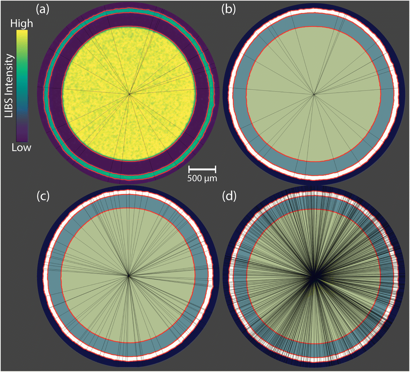 | ||
| Fig. 1 Example layer thickness calculation being applied to a Zr particle with random line profiles stemming from the median centroid: (a) contour boundaries (red lines) and line profiles (black lines) superimposed on the Zr 481.5 nm LIBS image from the ICCD spectrometer and (b)–(d) extracted contours used for the calculation with n = 25, 100, and 1000 line profiles, respectively. Each line profile's intersections with the red contour boundaries are used for calculating the layer thicknesses and their corresponding statistics. | ||
The number of profiles used in the thickness measurement tool was investigated prior to comparing the thicknesses determined with each measurement mode. The number of random profiles was varied from 5 to 1,000, with 10 replicates each, to compare the impact on the average uncertainty and the precision of the measured layer thickness. Fig. 2 shows the average % RSD of the thickness measurements and the precision of the mean thickness (n = 10 replicates) as a function of the number of profiles for all three layers. A few clear trends were identified. The greater the number of profiles used, the lower the uncertainty in the layer thickness and the higher the precision in the mean thickness. Logically, if too few profiles were used, then the tool would not fully capture the variance of the outer layer. Generally, the precision of the mean continued to decrease proportionally to the inverse of the square root of the number of profiles. This indicates that 1000 profiles should be used in the thickness measurement tool to obtain the most precise thickness measurements for these particles. Another interesting finding was that the % RSD values for all ICCD measurements were lower than their CMOS counterparts. This can likely be attributed to the better spatial resolution and sensitivity to boundaries between layers when mapping samples with the ICCD spectrometer. This effect was more pronounced for the core and intermediate PyC layer, but the thickness measurement of the outer layer relied on these inner dimensions, so this improvement may have compounded.
 | ||
| Fig. 2 The effect of the number of profiles used for the thickness measurement tool on (a), (c) and (e) the % RSD of the thickness and (b), (d) and (f) the % RSD of the mean thickness between replicates. The plot rows correspond to (a) and (b) the particle core, (c) and (d) the PyC intermediate layer, and (e) and (f) the ZrC outer layer. | ||
3.2. Zirconium carbide particle measurements
A set of nine ZrC surrogate TRISO particles with outer layers ranging in thickness from 16 to 32 μm were analyzed using SEM and LIBS to evaluate the thickness measurement tool. Both the CMOS and ICCD spectrometers were used to compare the accuracies of thicknesses measured with a broadband spectrometer with a larger spot size with those of a narrow-wavelength spectrometer with a reduced spot size. The LIBS spectra from line scans starting beyond the particle's outer layer and passing into the core are shown in Fig. 3 for both spectrometers.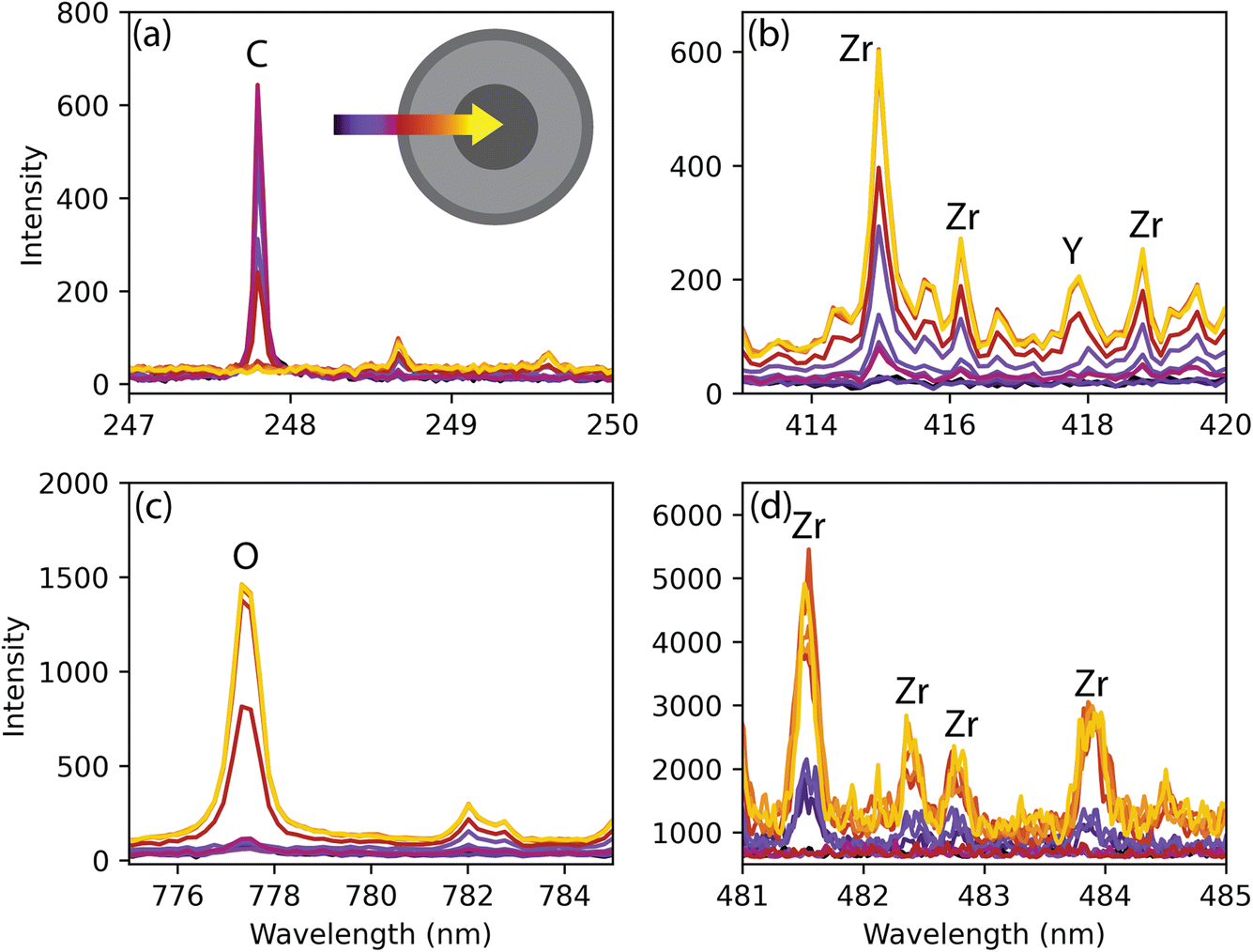 | ||
| Fig. 3 Comparison of (a)–(c) CMOS and (d) ICCD spectra from line scans across multiple ZrC particle layers. The spectra are colored according to the key shown in (a). As seen when comparing the intensities of Zr in (b) and (d), the ICCD was far more sensitive. | ||
The CMOS measurements were made at 200 Hz with a 20 μm square spot and 16 μm overlap (i.e., an effective resolution of 4 μm). Overlap between ablation spots, also known as dosage, has been demonstrated to increase spatial resolution while maintaining a spot size large enough for effective LIBS signals.26 With an 80% overlap in both directions, the dosage for these CMOS measurements was 25 shots per spot. This provided a broadband elemental map in less time, with an individual particle being mapped in 6 min. However, this spectrometer was less sensitive than the ICCD as illustrated when comparing Fig. 3(b) and (d). The ICCD measurements were taken at 90 Hz with a 7 μm square spot and a 5 μm overlap (i.e., an effective resolution of 2 μm). The ICCD collection settings corresponded to a dosage of 12 shots per spot. It is important to note this spot size was not possible using the CMOS spectrometer given the decrease in emitted light from the smaller plasma. The use of the ICCD with the smaller ablation spot size generated maps with 50% higher spatial resolution than the CMOS maps and greater sensitivity at the interfaces between layers, although these measurements took 22 min per particle, a 267% increase in measurement time compared with the CMOS. To better understand the benefit of this time-resolution trade-off, the accuracies of the layer thicknesses determined from both measurement modes were compared. Note that both LIBS measurements saved significant time compared with SEM-EDS measurements, which took approximately 2 h per particle; the CMOS and ICCD reduced the measurement time by 95% and 81.7%, respectively, compared with SEM-EDS mapping. Given that this reduction in time is for a single particle, when multiple particles are considered the time savings would compound whereas the sample preparation time would remain constant for up to roughly 30 particles per mount.
The nine Zr particles were analyzed with SEM-EDS and then mapped with both the CMOS and ICCD collection configurations. The Zr elemental maps of selected particles using each technique are shown in Fig. 4. The strongest Zr emission peaks without spectral interferences were selected for each spectrometer (414 nm and 481 nm for the CMOS and ICCD, respectively). Weaker emission peaks provided similar maps; however, the layer interfaces were less sharp due to their reduced response. The sharpness in layer boundaries in the ICCD maps differed starkly from the CMOS results. This can be attributed to the increased sensitivity and higher spatial resolution. The ICCD maps more closely resembled the quality of the SEM-EDS maps; however, the CMOS maps still provided the spatial distribution needed to extract layer dimensions. Because these Zr particles differed in their outer-layer thicknesses, the following comparison of the measurements focuses on this outer layer. The measured thickness of the PyC layer and the measured core diameter agreed with the SEM-EDS values (55.5 ± 10.45 and 229 ± 58 μm, respectively) regardless of the measurement mode (see Tables S1 and S2‡). Note that because samples were cross-sectioned and mounted, the core and PyC layer dimensions were more subject to effects of not being at the true center plane of the sample; however, the outer ZrC layer was less affected given its distance from the center of the spherical particle.
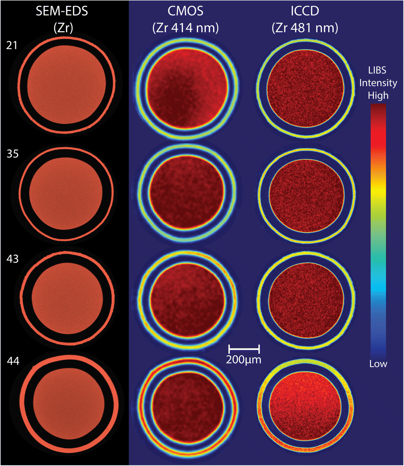 | ||
| Fig. 4 SEM-EDS, CMOS, and ICCD maps of Zr distribution in ZrC particles with outer layers ranging from 16 to 32 μm. | ||
The ZrC layer dimensions were calculated using n = 1000 profiles. The threshold value used to fine-tune thickness measurement accuracy was varied between 0.2 and 0.45. Values outside this range did not result in proper contour mapping. The results for the thickness tool processing of the CMOS and ICCD measurements as a function of threshold value are shown in Fig. 5. Notably, the CMOS quantities varied more as a function of threshold value compared to the ICCD values. This was likely due to the differences in the spatial resolution and sensitivity of the ICCD spectrometer more sharply increasing the signal intensity at the layer interface. Despite this, the SEM-EDS values could be used to determine an optimal threshold value for each measurement mode. Thresholds of 0.4 and 0.25 were determined to provide the most accurate results for the CMOS and ICCD measurements, respectively. These thickness values are shown in Table 1.
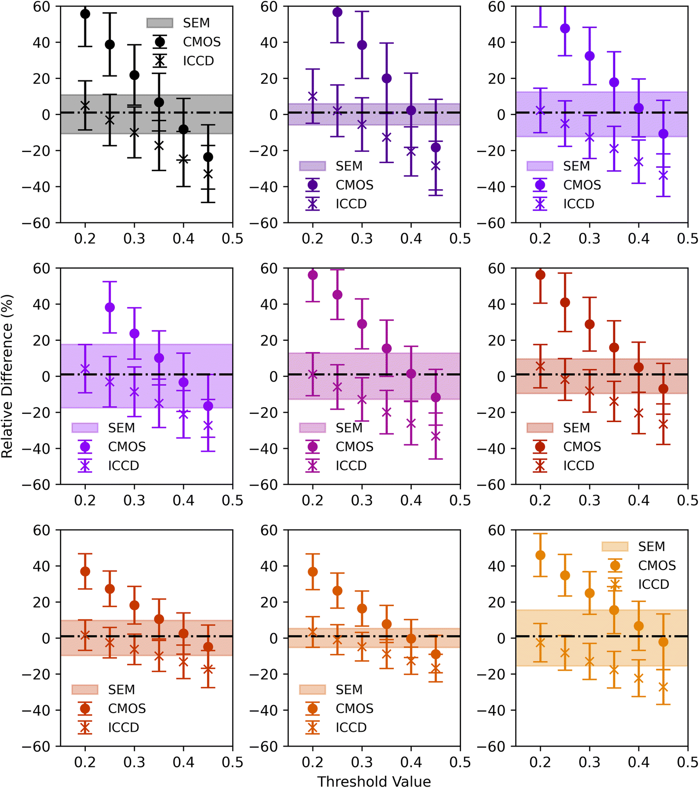 | ||
| Fig. 5 Percent relative differences between the CMOS- and ICCD-determined ZrC layer thicknesses and SEM-EDS values as a function of thickness tool threshold. Each subplot represents a different particle. The dashed lines indicate the SEM-EDS mean thickness values. The shaded regions represent the SEM-EDS uncertainties (2SD), and the error bars represent the LIBS uncertainties (2SD). | ||
| Sample tag | ZrC layer thickness (μm) | Zeta score |ζ| | |||
|---|---|---|---|---|---|
| SEM-EDS (manual) | CMOS (tool) | ICCD (tool) | CMOS | ICCD | |
| 21 | 19.4 ± 2.1 | 17.8 ± 3.3 | 18.8 ± 2.8 | 0.41 | 0.18 |
| 35 | 16.11 ± 0.95 | 16.5 ± 3.3 | 16.4 ± 2.3 | 0.11 | 0.13 |
| 40 | 19.1 ± 2.4 | 19.8 ± 3.1 | 18.1 ± 2.4 | 0.18 | 0.29 |
| 41 | 20.2 ± 3.5 | 19.5 ± 3.3 | 19.6 ± 2.8 | 0.14 | 0.14 |
| 42 | 20.0 ± 2.6 | 20.2 ± 3.0 | 18.8 ± 2.5 | 0.07 | 0.34 |
| 43 | 22.6 ± 2.2 | 23.7 ± 3.1 | 22.2 ± 2.6 | 0.30 | 0.12 |
| 44 | 33.8 ± 3.3 | 34.7 ± 3.9 | 33.0 ± 2.9 | 0.17 | 0.20 |
| 45 | 31.0 ± 1.6 | 30.9 ± 3.3 | 30.7 ± 2.6 | 0.03 | 0.10 |
| 46 | 31.6 ± 4.9 | 33.7 ± 4.3 | 29.0 ± 3.0 | 0.33 | 0.45 |
Using these threshold values, the SEM-EDS, CMOS, and ICCD measurements were all in agreement with one another. The uncertainties of the provided thickness measurements were similar, with average % RSD values of 11.1%, 14.4%, and 12.1% for the SEM-EDS, CMOS, and ICCD approaches, respectively. The uncertainties for LIBS-based measurements (n = 1000) were likely limited based on the true variance of the deposited layer itself. Note that the thickness measurement tool eliminates user bias in the measurement of layers because all profiles randomly radiate from the center of the particle with much larger sampling statistics, whereas the manual SEM-EDS measurements rely on the user selecting measurement points. Furthermore, the average values for % RD between the SEM-EDS results and the CMOS and ICCD measurements were 3.7% and 5.3%, respectively. To better compare the measured values, the zeta scores were calculated. A zeta score with an absolute value less than 1 represents strong consistency between the anticipated value (SEM-EDS) and the experimental value (LIBS). Both the CMOS and ICCD results had zeta scores well below 1. Overall, the CMOS measurements are the preferred approach because their results are consistent with SEM-EDS while providing broadband elemental coverage at rapid testing rates.
3.3. Tungsten particles
In addition to the Zr particles, a set of W surrogate TRISO particles were tested using the same methods. The W particles consisted of two more layers with more complex elemental compositions. Based on the results from the Zr particles, the W particles were mapped using a 20 μm spot size and a 16 μm overlap (i.e., an effective resolution of 4 μm and a dosage of 25 shots per spot). Preliminary testing revealed the CMOS had reduced sensitivity to the W outer layer. This may have been due to a decreased ablation efficiency as seen in a recent study by Maeda et al. when pure metal phases were being ablated.27 To overcome this, the ICCD was operated simultaneously with the CMOS. The ICCD spectral window was centered at 505 nm. This provided the broadband coverage of the CMOS and the sensitivity of the ICCD when needed. Because the W particles were roughly 150% larger than the previously discussed Zr particles, the maps were generated in 17 min, although the mapping rate was the same as for the Zr particles. Red–green–blue maps of the W particles are shown in Fig. 6. The corresponding SEM-EDS maps are provided in Fig. S2.‡ Clearly, the simultaneous CMOS and ICCD configuration provided well-resolved maps of all major layers. (The black intermediate regions in Fig. 6 correspond to the outer PyC layers.). The only difficult-to-measure layer was the inner PyC layer (approximately 12 μm) situated between the core and the Si layer. Although its location can be seen in Fig. 6, the inner PyC layer is not well resolved. Fig. S3‡ shows a cross-sectioned 3D rendering of the C 247 nm emission intensity in both color and height. In this figure, the inner PyC layer is visible, but its magnitude is significantly reduced compared with the outer PyC layer. This is largely due to its small dimensions relative to the laser spot size.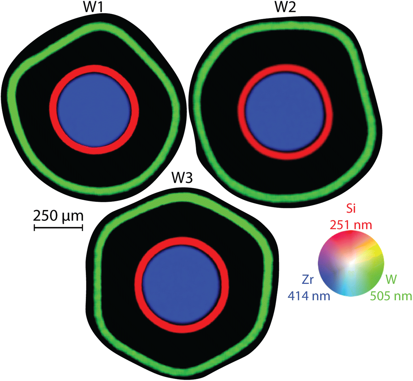 | ||
| Fig. 6 Red-green-blue maps of the W particles, in which red represents Si (CMOS), blue represents Zr (CMOS), and green represents W (ICCD). The black intermediate layers correspond to the outer PyC layers. | ||
The thickness measurement tool was used to extract the core radius and layer dimensions for each of these particles. Threshold values were toggled in a similar manner as in the Zr particle study until all layers converged about their SEM-EDS expected values. The core radius was determined using the Zr 414 nm CMOS data with a threshold of 0.6. The Si layer thickness was determined from the Si 251 nm CMOS data with a 0.6 threshold. The inner PyC layer could not be readily detected by the thickness tool because of its limited intensity; however, the difference between the internal radius of the Si layer and the previously calculated Zr core radius was used to infer the inner PyC layer thickness. The outer PyC layer dimensions were calculated with the C 247 nm CMOS data and a 0.4 threshold value. Lastly, the W 505 nm ICCD data were used to determine the thickness of the outer layer using a 0.5 threshold. All values were calculated using 1000 profiles. The thickness tool results are compared with SEM-EDS values in Table 2.
| Particle | Layer radius/thickness (μm) | ||||
|---|---|---|---|---|---|
| Core | Inner PyCa | Si | Outer PyC | W | |
| a LIBS inner PyC values were calculated from the differences between core radii and Si layer inner diameter values from the thickness tool. | |||||
| W1 (SEM-EDS) | 201.1 ± 2.2 | 12.0 ± 2.5 | 37.7 ± 2.8 | 186 ± 33 | 47.6 ± 3.1 |
| W1 (LIBS) | 204.7 ± 4.2 | 11.6 ± 5.2 | 36.7 ± 3.1 | 182 ± 32 | 49.1 ± 7.3 |
| W2 (SEM-EDS) | 201.3 ± 3.0 | 12.0 ± 2.2 | 38.3 ± 2.6 | 191 ± 29 | 48.0 ± 4.5 |
| W2 (LIBS) | 204.2 ± 5.1 | 11.7 ± 5.9 | 38.0 ± 2.9 | 195 ± 25 | 51.3 ± 5.9 |
| W3 (SEM-EDS) | 199.9 ± 1.5 | 14.9 ± 2.3 | 38.1 ± 3.5 | 173 ± 15 | 47.8 ± 3.9 |
| W3 (LIBS) | 203.2 ± 3.1 | 13.3 ± 4.0 | 38.4 ± 2.6 | 192 ± 25 | 49.1 ± 7.9 |
| Avg (SEM-EDS) | 200.8 ± 1.2 | 13.0 ± 1.3 | 38.0 ± 1.7 | 183 ± 13 | 47.8 ± 2.1 |
| Avg (LIBS) | 204.0 ± 2.2 | 12.2 ± 2.8 | 37.7 ± 1.6 | 189 ± 16 | 49.8 ± 4.0 |
Overall, the thickness tool – determined dimensions agreed with the values manually measured with SEM-EDS, with an average % RD of 2.7%. All zeta values for both individual particle layer thicknesses were in agreement (<1) between the methods. The average % RSD values for the LIBS measurements were below 10% for all layers except the inner PyC layer. This exception was due to the propagated uncertainty for the inner PyC, which was due to the inner PyC being calculated from the core and Si layer measurements. The largest differences between the SEM-EDS and LIBS values were in the two outermost layers. This can be attributed to the nonsymmetric shape of the outer PyC and W layers (Fig. 6). Using a greater number of profiles in the thickness tool likely leads to a more representative measurement of the variance of the PyC layer. Despite its nonsymmetric shape, the W layer appeared relatively uniform in thickness. The increased variance in the LIBS data may have been due to the profiles stemming from the center of the particle and not necessarily passing through the W layer perfectly perpendicularly to the interfaces. In terms of production monitoring, this measured variance may prove beneficial by aiding in diagnosing particle batches with large amounts of asymmetry.
4. Conclusion
This work expanded upon a previous proof-of-concept study and demonstrated how high-resolution LIBS mapping capabilities combined with a newly developed image analysis tool can enhance mapping capabilities for surrogate TRISO particles. Surrogate Zr TRISO particles made with layers of different thicknesses were mapped using SEM-EDS and LIBS. The new thickness tool, now embedded within iolite 4, successfully extracted layer dimensions (roughly ranging from 10 to 250 μm). The CMOS analysis of the Zr particles demonstrated measurement accuracy (3.7% RD), precision (<15% RSD), and decreased measurement times (−95%) relative to SEM-EDS, showing that LIBS can enable the elemental analysis and layer dimensional analysis needed to monitor TRISO production quality sufficiently. Note, this level of precision is interpreted as the natural variance in the layers themselves.The analysis of more complex surrogate TRISO particles further demonstrated the value of LIBS mapping with simultaneous CMOS and ICCD spectrometers. These W particles were mapped in 17 min, and the layer elemental compositions and spatial dimensions were extracted with an average % RD of 2.7% and an average % RSD of 9%. Because LIBS saves time compared with SEM-EDS, and because of the other characteristics of LIBS (e.g., fieldable, low capital and operational costs, wide elemental coverage), LIBS could be used for monitoring production batches on-site. This would enable rapid research and development on chemical vapor deposition effects on layer thicknesses (as demonstrated with the Zr particles) and permit quality assurance on existing procedures. For typical batches consisting of thousands of particles, rapid analysis would be necessary for quality control. Continued studies applying image analysis tools to LIBS mapping applications can further extend the applicability of LIBS over a range of solid-sample opportunities. Elemental quantification, although not a focus of this study, could also be readily implemented. The measurement of major and trace element compositions could be readily implemented within this workflow. Lastly, as research and development on TRISO fuel continues, the methods presented here can be used to analyze fuel after irradiation to examine layer performance and fission product distributions and could even be coupled with LA-ICP-MS for monitoring isotope ratios.
Data availability
Data is available upon reasonable request.Author contributions
Conceptualization (H. A., B. M.), data curation (H. A., D. Q., T. B., B. M.), formal analysis (H. A., T. B.), funding acquisition (B. M.), investigation (H. A., D. Q., T. B., J. P., B. P., P. D., B. M.), methodology (H. A., J. P., B. P., B. M.), visualization (H. A.), writing – original draft (H. A., B. M.), writing – review & editing (H. A., D. Q., T. B., J. P., B. P., P. D., B. M.)Conflicts of interest
D. Q., J. P., and B. P. declare that they are currently in the employ of Elemental Scientific Inc., the company that sells the underlying software (iolite) used in this work. This does not, in their opinion, affect the underlying principles and advances described herein.Acknowledgements
This work was supported by Oak Ridge National Laboratory (ORNL), managed by UT-Battelle for the US Department of Energy under contract DE-AC05-000R22725. This work was supported by ORNL's Laboratory Directed Research and Development Program. The authors would like to acknowledge Jacquelyn Demink (ORNL) for assistance with graphics, Peter Doyle (ORNL) for assistance in acquiring test samples, and Christopher Hobbs (ORNL) for assistance with TRISO mounting.References
- L. Jolivet, M. Leprince, S. Moncayo, L. Sorbier, C.-P. Lienemann and V. Motto-Ros, Spectrochim. Acta, Part B, 2019, 151, 41–53 CrossRef CAS.
- V. Lednev, P. Sdvizhenskii, A. Dorohov, S. Gudkov and S. Pershin, Appl. Opt., 2023, 62, 2030–2038 Search PubMed.
- R. Finotello, M. Tamaazousti and J.-B. Sirven, Spectrochim. Acta, Part B, 2022, 192, 106418 Search PubMed.
- H. B. Andrews, C. D. Quarles Jr, V. C. Bradley, T. L. Spano, J. A. Petrus, B. Paul, N. A. Zirakparvar, D. R. Dunlap, C. R. Hexel and B. T. Manard, Microchem. J., 2024, 196, 109605 Search PubMed.
- A. Limbeck, L. Brunnbauer, H. Lohninger, P. Pořízka, P. Modlitbová, J. Kaiser, P. Janovszky, A. Kéri and G. Galbács, Anal. Chim. Acta, 2021, 1147, 72–98 Search PubMed.
- K. Rifai, F. Doucet, L. Özcan and F. Vidal, Spectrochim. Acta, Part B, 2018, 150, 43–48 CrossRef CAS.
- D. W. Hahn and N. Omenetto, Appl. Spectrosc., 2012, 66, 347–419 CrossRef CAS.
- E. H. Kwapis, J. Borrero, K. S. Latty, H. B. Andrews, S. S. Phongikaroon and K. C. Hartig, Appl. Spectrosc., 2024, 78, 9–55 Search PubMed.
- R. L. Seibert, B. C. Jolly, M. Balooch, D. P. Schappel and K. A. Terrani, J. Nucl. Mater., 2019, 515, 215–226 CrossRef CAS.
- K. Minato, T. Ogawa, K. Sawa, A. Ishikawa, T. Tomita, S. Iida and H. Sekino, Nucl. Technol., 2000, 130, 272–281 CrossRef CAS.
- K. Sanyal, S. Dhara, S. Sanjay Kumar, N. Misra, P. Mollick, P. Rao, R. Venugopalan, R. V. Pai, N. Kumar and S. Mukerjee, J. Radioanal. Nucl. Chem., 2014, 302, 1357–1361 Search PubMed.
- K. Kiegiel, I. Herdzik-Koniecko, L. Fuks and G. Zakrzewska-Kołtuniewicz, Energies, 2022, 15, 1099 CrossRef CAS.
- P. Doyle, E. Lopez-Honorato, G. Vasudevamurthy, J. Miller, H. Meyer III and T. Gerczak, J. Nucl. Mater., 2024, 594, 155019 Search PubMed.
- S. Van der Walt, J. L. Schönberger, J. Nunez-Iglesias, F. Boulogne, J. D. Warner, N. Yager, E. Gouillart and T. Yu, PeerJ, 2014, 2, e453 Search PubMed.
- N. Rohbeck and P. Xiao, Nucl. Eng. Des., 2016, 306, 52–58 CrossRef CAS.
- I. E. Porter, T. W. Knight, M. C. Dulude, E. Roberts and J. Hobbs, Nucl. Eng. Des., 2013, 259, 180–186 Search PubMed.
- E. Chajduk and P. Kalbarczyk, Nukleonika, 2021, 66, 121–126 Search PubMed.
- J. P. de Villiers, J. Roberts, N. Ngoepe and A. S. Tuling, J. Eng. Gas Turbines Power, 2009, 131, 062904 Search PubMed.
- D. Spanu, A. Palestra, V. Prina, D. Monticelli, S. Bonanomi, S. U. Nanot, G. Binda, L. Rampazzi, G. Sessa and D. Callejo Munoz, Molecules, 2023, 28, 2845 CrossRef CAS PubMed.
- B. T. Manard, H. B. Andrews, C. D. Quarles, V. C. Bradley, P. Doyle, N. A. Zirakparvar, D. R. Dunlap and C. R. Hexel, J. Anal. At. Spectrom., 2023, 38, 1412–1420 RSC.
- D. Roberts, A. Du Plessis, J. Steyn, L. Botha, C. Strydom and I. Van Rooyen, Spectrochim. Acta, Part B, 2010, 65, 918–926 CrossRef.
- J. Gonzalez, X. Mao, J. Roy, S. Mao and R. Russo, J. Anal. At. Spectrom., 2002, 17, 1108–1113 RSC.
- B. T. Manard, C. D. Quarles Jr, V. C. Bradley, T. L. Spano, N. A. Zirakparvar, B. W. Ticknor, D. R. Dunlap, P. Cable-Dunlap, C. R. Hexel and H. B. Andrews, J. Am. Chem. Soc., 2024, 146, 14856–14863 CrossRef CAS PubMed.
- C. Paton, J. Hellstrom, B. Paul, J. Woodhead and J. Hergt, J. Anal. At. Spectrom., 2011, 26, 2508–2518 RSC.
- M. A. d. M. Franco, D. M. B. P. Milori and P. R. V. Boas, arXiv, 2018, preprint, arXiv:1805.03695, DOI:10.48550/arXiv.1805.03695.
- D. K. Gibbs, M. Podsednik, P. Tapler, M. Weiss, A. K. Opitz, M. Nelhiebel, C. D. Quarles Jr, S. Larisegger and A. Limbeck, Chem. Biomed. Imaging, 2024, 2, 631–639 CrossRef CAS PubMed.
- R. Maeda, T. Van Acker, F. Vanhaecke, A. Yamaguchi, V. Debaille, P. Claeys and S. Goderis, J. Anal. At. Spectrom., 2023, 38, 369–381 RSC.
Footnotes |
| † This manuscript has been authored in part by UT-Battelle, LLC, under contract DE-AC05-00OR22725 with the US Department of Energy (DOE). The US government retains and the publisher, by accepting the article for publication, acknowledges that the US government retains a nonexclusive, paid-up, irrevocable, worldwide license to publish or reproduce the published form of this manuscript, or allow others to do so, for US government purposes. DOE will provide public access to these results of federally sponsored research in accordance with the DOE Public Access Plan (http://energy.gov/downloads/doe-public-access-plan). |
| ‡ Electronic supplementary information (ESI) available. See DOI: https://doi.org/10.1039/d4ja00471j |
| This journal is © The Royal Society of Chemistry 2025 |