
 Open Access Article
 This Open Access Article is licensed under a Creative Commons Attribution-Non Commercial 3.0 Unported Licence
Low-emissivity fine-tuning of efficient VO2-based thermochromic stacks with silver nanowire networks†
Amaury
Baret
 *a,
Ambreen
Khan
bc,
Aline
Rougier
c,
Daniel
Bellet
b and
Ngoc Duy
Nguyen
a
*a,
Ambreen
Khan
bc,
Aline
Rougier
c,
Daniel
Bellet
b and
Ngoc Duy
Nguyen
a
aDepartment of Physics, SPIN, University of Liège, Allée du Six Août 19, Liège B-4000, Belgium. E-mail: abaret@uliege.be
bUniv. Grenoble Alpes, CNRS, Grenoble INP, LMGP, Grenoble F-38016, France
cUniv. Bordeaux, CNRS, Bx INP, ICMCB, UMR5026, F-33600 Pessac, France
First published on 4th October 2024
Abstract
In response to the urgent need for environmentally sustainable alternatives to combat climate change, considerable attention has been directed towards the development of functional materials for energy management. Among these, thermochromic-based smart windows have emerged as a significant area of interest due to their ability to dynamically and passively regulate the amount of sunlight entering a building while maintaining consistently high visible transmittance. Additionally, low thermal emissivity is crucial for energy efficiency in cold climates. In this theoretical study, we numerically explore the application of silver nanowire networks as a low infrared emissivity coating to enhance the performance of VO2-based thermochromic multilayer stacks. We propose a highly efficient thermochromic stack capable of achieving a luminous transmittance of 79% and a solar modulation ability of 15.7%, while simultaneously exhibiting an infrared emissivity as low as 8%. Via the addition of the Ag NW network, we show that it is also possible to reduce the emissivity of VO2 nanoparticle-based stacks up to 20% while keeping a FOM higher than 0.01, which we show is not possible by using a Ag thin film alone.
1 Introduction
In 2019, the heating and cooling of buildings accounted for 35% of humanity's net energy use.1 Windows constitute major contributors to heat exchange between buildings and their surroundings, motivating extensive research into improving their energy performance. Amongst the several approaches that have been explored to address energy losses through buildings, smart windows have attracted significant attention thanks to their ability to dynamically modulate light transmission.2 Central to the functionality of smart windows are chromogenic materials, which exhibit dual transparency states. These materials typically modify their transmittance spectra based on external factors such as temperature (thermochromics), voltage (electrochromics), or light (photochromics). Thermochromic materials, in particular, have garnered significant interest owing to their passive thermal switching capabilities between opaque and transparent states in the infrared (IR) part of the electromagnetic spectrum. Vanadium dioxide (VO2), which presents a reversible thermally triggered first-order transition from an insulating to a metallic crystalline structure, stands out as the most prevalent and extensively studied thermochromic material.3,4 Its transition is accompanied by a significant shift in transmittance, primarily affecting the near-infrared (NIR) part of the spectrum. While an ideal smart window would maintain high visible light transmittance (Tlum) under any conditions, it would simultaneously act as a spectrally selective filter, allowing the NIR spectrum during cool periods to maximize passive solar heating and blocking NIR transmission during warm periods. VO2 exhibits remarkable properties that align closely with this ideal behavior. It simultaneously boasts high Tlum and solar modulation ability ΔTsol,5,6 but also presents the salient advantage of possessing a relatively low (68 °C) and dopant-adjustable (down to 32 °C) transition temperature (Tc),7,8 making it a prime candidate for the development of efficient and versatile thermochromic smart windows. VO2-based thermochromic stacks typically consist of multilayer film stacks, with anti-reflection (AR) layers commonly incorporated to mitigate reflectance in the visible spectrum.9–12 While SiO2 and TiO2 are amongst the most popular AR layers,13–15 numerous others, including Si3N4,16 ZnO,17 Cr2O3,18 and CeO2,19 have been explored. Despite their varied compositions, they share the common objective of smoothing the refractive index gradient from air (n = 1) to VO2 (n > 2 in the visible range), a technique commonly referred to as optical impedance matching. Another well-known method to enhance the thermochromic properties of VO2-based stacks consists in substituting the VO2 thin film layer with an equivalent film of VO2 nanoparticles (NPs) embedded in a transparent polymer such as PET or PVP.20,21 This idea was first proposed by Li et al. in their seminal paper from 2010.22 Their theoretical and numerical prediction has been extensively corroborated in the literature,5,23–25 with recent results from Li et al. demonstrating the aforementioned simultaneous improvements in both Tlum (>90%) and ΔTsol (>10%).26Another important parameter to consider when designing smart windows is their thermal emissivity ε.27 Minimizing ε, specifically within the long-wave infrared (LWIR) region, is crucial as this part of the spectrum (2.5 μm < λ < 20 μm) aligns with the black-body radiation of objects at typical indoor temperatures. As a consequence, heat exchanges from the inside of the building to the outside are kept to a minimum, thereby maximizing the window's insulating capacity and enhancing its potential for energy savings in cold-climate regions. Low-emissivity coatings are commonly achieved by using metallic thin films.28 These films offer a balance – they are thin enough to maintain high visible transmittance yet sufficiently thick to increase the infrared reflectance, effectively lowering the emissivity. Several studies have explored this approach for VO2-based thermochromic stacks. Benkahoul et al. were pioneers in using metallic films for emissivity control and discovered that the IR reflectance of the stack depends on the substrate's properties.29 While vanadium dioxide (VO2) naturally exhibits increased reflectance (and thus lower emissivity) in its metallic state on transparent substrates such as glass, the opposite occurs when deposited onto a metallic layer. This so-called positive switching emissivity behavior, which is crucial for applications in heat management30,31 and spacecraft thermal control,32,33 can be attributed to the Fabry–Pérot effect, which is absent when VO2 is in its dielectric state.34 Kang et al. successfully used a thin platinum film to achieve ε as low as 45%,35 while Baloukas et al. later demonstrated that adding a thin layer film not only lowers the emissivity (with achieved ε = 10%) but can also enhance the solar modulation without impacting the luminous transmittance.16
Concurrently, there has been a recent surge of interest in the low emissivity (low-ε) characteristics of silver nanowire (Ag NW) networks.36,37 These networks are commonly utilized as transparent electrodes, showing excellent electro-optical properties alongside the notable advantage of flexibility. Additionally, they can be produced using cost-effective and scalable techniques such as roll-to-roll coating38,39 and easily coated with protective oxides such as ZnO or SnO2 to enhance their stability.40,41 These advantages, combined with their low-ε properties, have prompted Zhao and colleagues to propose a thermochromic stack comprising VO2 on glass coated with Ag NWs to reduce the emissivity42 up to 0.6. Despite pioneering this novel material combination, their research did not concentrate on the thermochromic characterization of the stack or on the utilization of an efficient and optimized stack. Furthermore, the potential of VO2 nanoparticle-based stacks was not explored. Consequently, we believe that there is an opportunity to improve upon their findings by investigating the addition of a low-ε Ag NW network deposited on top of a VO2-based thermochromic stack.
In this research, we numerically explore the application of Ag NW networks as low infrared emissivity coatings to enhance the performance of VO2-based thermochromic multilayer stacks. In the first section of this paper, we outline and justify the chosen theoretical and numerical methods used to simulate the stack's properties. We also introduce a new figure of merit (FOM) for quantifying a stack's thermochromic performance. Subsequently, we detail the multi-layer thickness optimization process and quantify the resulting properties, aiming to achieve a maximum FOM stack with a target low-emissivity value. This optimization procedure is performed for both VO2 thin film-based and nanoparticle-embedded-in-PET stacks, from here on referred to as TF and NP stacks, respectively. Finally, we analyze the impact of adding a Ag NW network on top of the stack, quantifying its influence on the emissivity, Tlum, and ΔTsol, elucidating the inherent trade-offs involved while providing a tool for fabricating and designing smart windows with the desired properties.
2 Methods
2.1 Investigated properties and FOM introduction
To characterize the optical (visible) transmittance of the investigated stacks, we utilize the quantity Tlum, which is a property defined on the visible spectrum: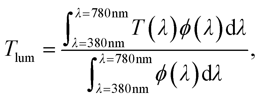 | (1) |
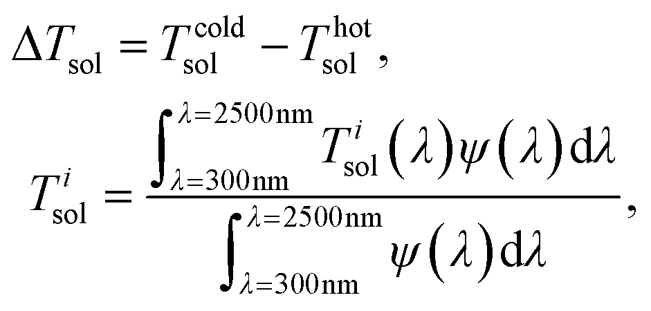 | (2) |
In an ideal scenario, the goal is to optimize both Tlum and ΔTsol simultaneously to achieve maximum visible transparency and energy efficiency, respectively. However, practical implementation reveals a well-established trade-off between these factors, wherein an increase in one property leads to a decrease in the other. Thus, a careful balance must be struck to identify the most favorable combination of Tlum and ΔTsol. In order to identify the most-optimized set, the use of a figure of merit (FOM) thus appears natural. Sol et al. introduced the following FOM:10
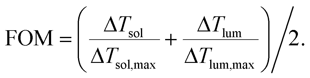
| FOM = ΔTsol × T4lum. | (3) |
The emissivity in the long-wave infrared (LWIR) region is typically defined according to the following equation:
 | (4) |
| ε(λ) = α(λ) = 1 − R(λ) − T(λ), | (5) |
While eqn (4) and (5) allow for the calculation of the total emissivity of multilayer stacks if their reflectance and transmittance spectra are known, it is not directly applicable when the stack is covered with nanowires (NWs) due to their inherently strong anisotropy and unknown refractive indices in the LWIR. Consequently, this method can only be used to determine the emissivity of the NW-less stack.
To obtain the total emissivity of the NW-coated stack, we thus employ the semi-empirical model developed by Hanauer et al.,45 which aligns with experimental results from the literature:37,46
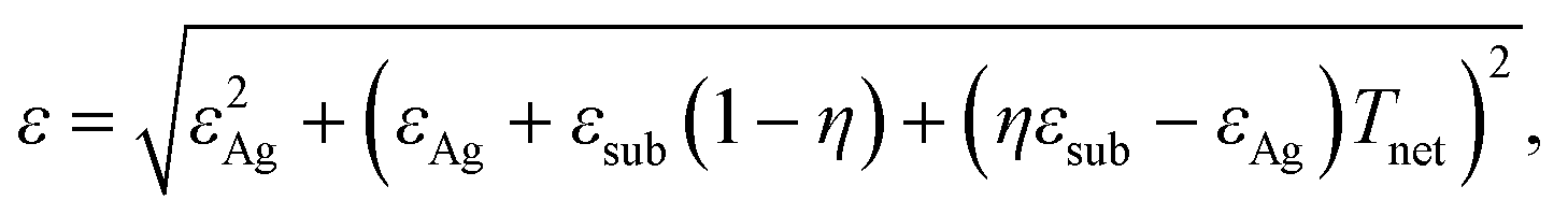 | (6) |
2.2 Numerical simulations
To determine the reflectance R(λ) and transmittance T(λ) spectra of the examined stack, the transfer-matrix method49–51 (TMM) was employed, utilizing the Python implementation of the tmm package.52 This numerical scheme is widely recognized in optics,53 particularly in the field of anti-reflection coatings. It involves solving Fresnel's equations at each interface within a given stack while accounting for light absorption within the layers themselves. The solutions provided by this model are analytically exact, revealing interference patterns in the obtained spectra. Experimental results, in contrast, lack these fringes due to various coherence-disrupting factors inherent to real materials, such as surface roughness and inhomogeneity.54 To best reflect empirical results, incoherent simulations are essential, focusing solely on the reflection, absorption and transmission of the power densities at the interfaces without considering the amplitudes of the light waves and, consequently, their interferential effects. In this study, partially incoherent simulations were performed: incoherent calculations were applied to simulate light propagation in the incoming and sorting air layers, as well as in the thick substrate and PET-embedded NP layer, while coherent simulations were used for the propagation in the other thin films. Real and complex refractive indices (n and k, respectively) were retrieved from the literature to be used as inputs to the simulations thanks to the WebPlotDigitizer tool.55 In this work, the considered wavelength range spans from 300 to 20![[thin space (1/6-em)]](https://www.rsc.org/images/entities/char_2009.gif) 000 nm, encompassing both the visible and LWIR regions. Simulations were performed with a wavelength step of 1 nm, with a normal incidence angle. Given that literature data do not always align with this sampling frequency, any missing values were linearly interpolated. A summary of the data used for the simulations of the investigated stacks (excluding those used for Fig. 1, whose associated data are given in ESI† Table S1) is given in Table 1.
000 nm, encompassing both the visible and LWIR regions. Simulations were performed with a wavelength step of 1 nm, with a normal incidence angle. Given that literature data do not always align with this sampling frequency, any missing values were linearly interpolated. A summary of the data used for the simulations of the investigated stacks (excluding those used for Fig. 1, whose associated data are given in ESI† Table S1) is given in Table 1.
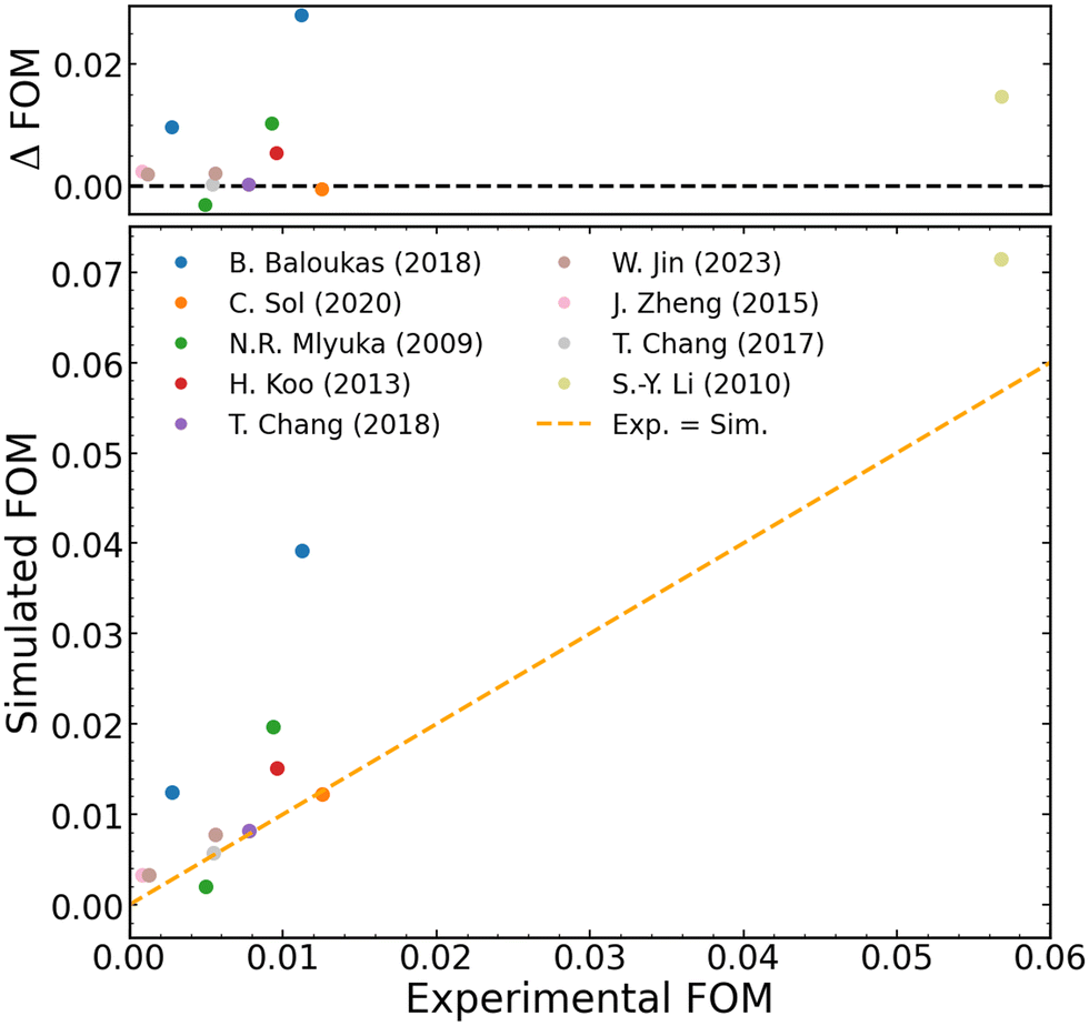 | ||
| Fig. 1 Simulated vs. experimental figure of merit (FOM) for different multilayer stacks found and studied in the literature. The top of the graph shows the difference between the simulated and experimentally measured values of the FOM. As expected, most FOMs are overestimated but are close to the ideal 0 line. Experimental data and stack structures were obtained from Baloukas et al.,16 Sol et al.,10 Mlyuka et al.,11 Koo et al.,19 Chang et al.,18 Jin et al.,17 Zheng et al.,56 Chang et al.,57 and Li et al.22 Baloukas et al. investigated two distinct stacks, which were both simulated. Comprehensive refractive index data sources and stack compositions can be found in ESI† Table S1. | ||
| Material | λ range (μm) | Notes | Ref. |
|---|---|---|---|
| VO2 TF | 0.3–2.5 | — | Mlyuka et al. (2009)58 |
| VO2 TF | 2.5–20 | — | Wan et al. (2019)59 |
| Ag TF | 0.3–2.5 | d > 6 nm | Zhao et al. (2009)60 |
| Ag TF | 2.5–20 | — | Ciesielski et al. (2017)61 |
| Fused SiO2 | 0.21–6.7 | — | Malitson (1965)62 |
| Fused SiO2 | 7–20 | — | Kitamura et al. (2007)63 |
| SiO2 TF | 0.25–2 | — | Gao et al. (2012)64 |
| SiO2 TF | 2–5 | — | Kischkat et al. (2012)65 |
| SiO2 TF | 5–20 | — | Herguedas et al. (2023)66 |
| TiO2 | 0.12–20 | — | Siefke et al. (2016)67 |
| PET | 0.4–2 | — | Zhang et al. (2020)68 |
| PET | 2–20 | — | Zhang et al. (2020)69 |
The refractive indices for the NP layer were determined analytically based on the values of the VO2 thin film, utilizing theoretical findings from Li et al.22 Employing the effective medium approach, they expressed the optical constants of the NP-embedded layer as a function of the VO2 thin film and polymer matrix refractive indices, the shape of the NPs, and the volume filling fraction f. Further elaboration on this approach and its use in this work can be found in the ESI.† To ensure a fair comparison between TF-based and NP-based stacks, when dealing with a NP layer, we chose to simulate an equivalent amount of VO2 in each stack. Consequently, the thickness of the NP stacks is 1/f times higher than that of the equivalent thin film, maintaining an equal total VO2 quantity. In the rest of this work, we express the NP VO2 layer's thickness as its equivalent thickness, such that a PET-embedded NP layer of d nm has an equivalent thickness of d × f. In this work, we considered spherical nanoparticles with a filling factor f = 0.01, which yields the highest thermochromic properties according to the results of Li et al.
To validate our numerical approach, we conducted simulations on multilayer stacks sourced from the existing experimental literature and compared our simulated results with those of the same stacks. The results of these comparisons are depicted in Fig. 1. In most instances, the similarity between our simulated data and experimental findings is striking, with negligible differences in the FOM for the majority of data points. However, certain results, particularly those from Baloukas et al.,16 deviate more from the ideal ‘x = y’ line. We attribute this variance to disparities in the quality of the deposited VO2 thin films with those utilized to determine the refractive indices used in our study. In general, variations in layer deposition quality and surface roughness can lead to experimental data rather different from the ideal simulated scenarios, especially evident in the upper segment of the graph where simulations tend to overestimate the FOM. This discrepancy is expected given the idealized conditions assumed in simulations. Nevertheless, these results confirm the suitability of transfer matrix method (TMM)-based numerical simulations for analyzing multilayer stacks in thermochromic applications. It is noteworthy that these validation results extend beyond our current study to encompass previous10,70–73 and forthcoming simulation endeavors from the literature, thus explicitly confirming the validity of the TMM approach to simulate thermochromic stacks and properties.
Additionally and as previously mentioned, the influence of the Ag NW network on the stack's optical properties cannot be computed via the TMM due to its highly anisotropic character. However, this limitation is not problematic because the nature of the NW network does not give rise to interference patterns, and the interface between the network and the underlying substrate thus plays a minimal role in the resulting optical behavior. Therefore, it is reasonable to assume that the transmittance of the Ag NW coated-stack equals the product of the transmittance values for the bare stack and the Ag NW network. Furthermore, as demonstrated by Atkinson et al.,74 the transmittance of Ag NW networks remains relatively constant across the wavelength range of 300 nm to 2500 nm, provided that the NW diameter is sufficiently large (>120 nm). Consequently, as a first approximation, we can assume a constant value for the network's transmittance Tnet and write the Tlum and ΔTsol values of a stack covered with a NW network as:
| Tlum = Tnet × Tlum,substrate | (7) |
| ΔTsol = Tnet × ΔTsol,substrate | (8) |
3 Results and discussion
3.1 Ag as a low-emissivity add-on
As detailed in section 1, our initial investigation focused on assessing the implications of incorporating a silver thin film beneath the VO2 layer, both within a thin film and a PET-embedded NP matrix. As depicted in Fig. 2(a), the behavior of the Ag layer aligns with findings from the existing literature when utilized alongside the thin film.16 For thin VO2 layers, the addition of silver notably enhances the FOM, increasing from 0.004 to >0.01 for a 7 nm Ag silver thin film. This enhancement in thermochromic properties stems from the augmented ΔTsol facilitated by the Ag layer, which does not lead to a decrease in visible transmittance for the relatively low Ag thicknesses investigated in this study but does make the interface with the VO2 layer more sensitive to its metallic/insulating switching, as shown by Baloukas et al.16 and detailed in section S4 of the ESI.† However, it is noteworthy that simulations conducted for Ag thicknesses ranging from 1 to 5 nm (inclusive) may overestimate the actual FOM. This is attributed to the rapid increase in both real and complex refractive indices of silver below 7 nm,75 resulting in heightened absorbance and reflectance of the Ag layer, consequently diminishing the overall thermochromic properties of the stack. Moreover, due to the well-known Volmer–Weber growth mode of the Ag layer,76 depositing such ultra-thin layers of silver poses significant experimental challenges. Consequently, results for Ag thicknesses in the 1–5 nm range should be disregarded in this investigation. The same argument applies to the NP stack.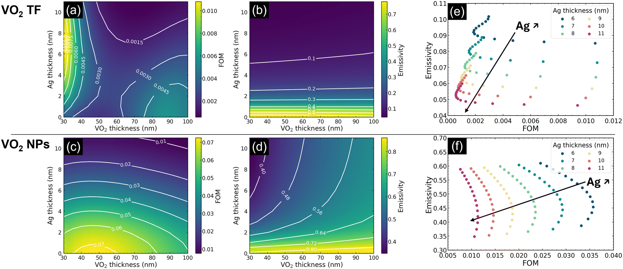 | ||
| Fig. 2 Summary of the parameter space investigation results for a VO2/Ag/fused-SiO2 stack. (a) and (c) FOM heatmap and isocontour maps for the stack with different combinations of Ag and VO2 thicknesses for the thin film (TF) and NP stacks, respectively. For the TF stack, the highest obtained FOM corresponds to Ag and VO2 thicknesses of 7 nm and 30 nm, respectively. In the NP stack, the highest FOM is obtained with Ag and equivalent VO2 thicknesses of 6 nm and 50 (5500 real) nm, respectively. (b) and (d) Emissivity ε heatmaps and isocontour maps for the stack with different combinations of Ag and VO2 thicknesses for the thin film (TF) and NP stacks, respectively. (e) and (f) Emissivity of the stack as a function of its FOM for different Ag thicknesses. | ||
As shown in Fig. 2(a), the optimal VO2 thickness in terms of FOM for the TF stack was determined to be 30 nm, the lowest simulated thickness in this work due to the known degradation of the solar modulation for very thin VO2 films.77 Given the design of the introduced FOM to be maximal for (Tlum, ΔTsol) = (75%, 20%), a 30 nm thick layer is found to be sufficient to achieve the required ΔTsol. Notably and as expected, increasing the VO2 thickness leads to a rise in ΔTsol at the expense of decreasing Tlum, and vice versa. In contrast to the TF stack and as displayed in Fig. 2(c), the addition of silver to NP stacks results in a unidirectional reduction of the FOM. Accordingly, the optimal Ag thickness for the NP stack is determined to be 0 nm when its FOM is the sole consideration. This divergent behavior from the TF stack is attributed to the considerably larger thickness of the NP layer, inducing an incoherent behavior of light propagation within the material, thereby nullifying the positive interferential effect at the VO2/Ag interface. Consequently, increasing the VO2 layer's thickness in the NP layer only amplifies its absorbance, thereby deteriorating both Tlum and ΔTsol, effectively decreasing the FOM value. The optimal FOM was achieved for a 55 nm equivalent thickness layer (5.5 μm of polymer-embedded matrix), underscoring the necessity for an additional VO2 material in embedded NPs to attain similar ΔTsol to those of the thin film case. In addition to FOM optimization, Fig. 2(b) and (d) illustrate the impact of the Ag film on the stacks' emissivities when VO2 is in its insulating state. It is also noteworthy that the addition of silver leads to a direct reversal of the emissivity switching sign in the TF stack, transitioning from εmet < εins (defined as the emissivity of the stack when VO2 is in the metallic and insulating state, respectively) for the Ag-less stack to Δε = εmet − εins > 0 when silver is added. Additionally, increasing the Ag layer's thickness results in the expected gradual decrease in emissivity, attributed to the enhanced reflectance of the stack in the IR domain with increasing Ag thickness. Considering the impact of the VO2 thickness, in the case of the TF-based stack, increasing the VO2 thickness has a minimal impact on the emissivity. In the case of the NP-based stack, given that the real thicknesses involved are larger, increasing the VO2 equivalent thickness leads to a non-negligible enhancement of the absorption in VO2, thus increasing the total emissivity. Based on these findings, it becomes evident that an optimal balance must be struck between the stack's emissivity and its FOM. In Fig. 2(e) and (f), we illustrate the variation of the emissivity for both TF and NP stacks as a function of their FOMs. The outcomes reveal distinct patterns that mirror the expression of the FOM. Notably, the behaviors of the NP and TF stacks differ significantly. For NPs, at a given Ag thickness, the FOM remains relatively stable, while the emissivity can nearly double by adjusting the VO2 thickness. The observed decreases in ε stem from the well-known increase in reflectance of increasingly thick metallic thin films, which is attributed to the destructive interferences occurring between the light waves reflected at the first and second interfaces of the film.75,78,79 With thicker layers, this interference starts to play a more negligible role, and the entirety of the light will eventually be reflected, thus leading towards lower emissivity values. Consequently, a tradeoff does exist between ε and the FOM in the case of NPs. Since our primary objective in this initial section is to maximize the FOM (with emissivity modulation primarily achieved by adding Ag NWs), we selected a Ag thickness of 7 nm for the NP stack. Conversely, in the TF stacks, it is apparent that the associated emissivities are considerably lower than those of the NP stack, albeit at the expense of a reduced FOM. Nevertheless, it's noticeable that for a given Ag thickness, it is the emissivity that remains consistently low, while the FOM exhibits more significant variation. This corresponds to the relatively monotonic increase in emissivity for any given VO2 thickness with the Ag thickness, as illustrated in the graph (Fig. 2(b)). Using the same rationale as that for the NP stacks, a Ag layer of 6 nm was deemed optimal.
3.2 Antireflection layers and optical impedance matching
After identifying the VO2 and Ag thicknesses that reach an optimum in FOM and emissivity values, we have studied the subsequent impact of the addition of double SiO2–TiO2 layers onto the previously optimized VO2/Ag/fused-SiO2 stack. The results of these layers' addition are displayed in Fig. 3. In both cases, the FOM is largely increased from the no-AR case, as also evidenced in Table 2. For the thin films, an optimum in FOM was found at (100, 40) nm for the SiO2 and TiO2 thicknesses, respectively. This optimum resonates with findings from the literature.10 Similarly, an optimum of (120, 20) nm was found for the NP-based stack. The pattern displayed in Fig. 3(a) and (c) for the FOM in terms of TiO2 and SiO2 thicknesses is typical for the use of these two materials and emerges because of the interference between the two layers. It is also worth noting that the impact of the addition of those two layers on the emissivity is limited, such that the (minimum, maximum) ε pairs for the SiO2/TiO2 coated stacks are (0.07, 0.09) and (0.45, 0.48) for the TF and NP stacks, respectively. The observed modest increase in ε is attributed to the increased absorbance of the stack due to the presence of the AR layers. The resulting transmittance and emissivity spectra of the stacks with optimal layer thicknesses are depicted in Fig. 3(b) and (d), with the AM1.5 spectrum provided as a reference. Notably, a more pronounced difference between the metallic and insulating transmittance spectra is observed in the case of NPs compared to TF, leading to a higher ΔTsol. Conversely, in terms of emissivity, a greater difference between the two states is noted for TF compared to NP stacks, albeit with positive emissivity switching in the TF stack, as anticipated and desired due to the presence of the Ag layer. Peaks in emissivity at 7500 and 10000 nm for the TF spectrum are attributed to the fused SiO2 substrate itself, with refractive indices varying in the LWIR part of the spectrum. Similarly, the seemingly chaotic appearance of the emissivity spectrum for NPs is predominantly influenced by the transmittance and reflectance spectra of the PET itself, as evidenced in Fig. S3 of the ESI.†
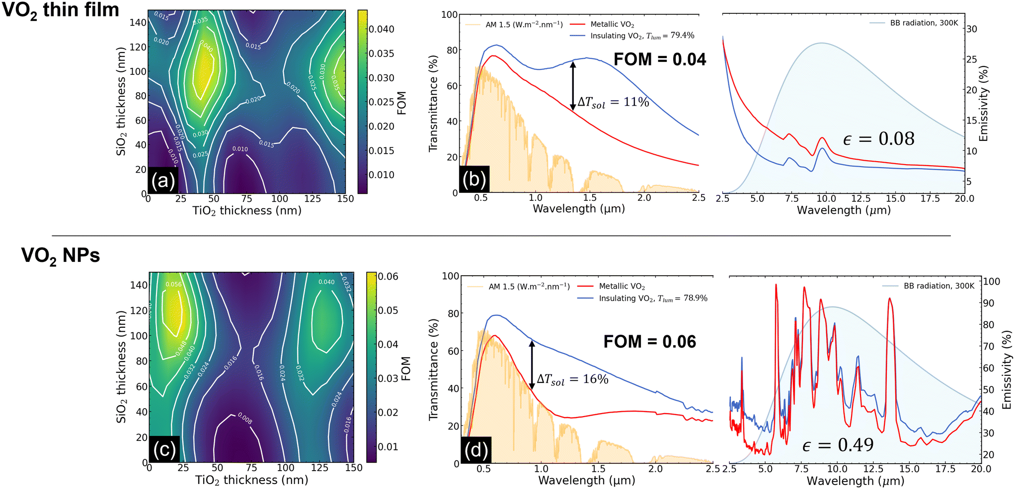 | ||
| Fig. 3 Results associated with the SiO2/TiO2/VO2/Ag/TiO2/SiO2 stack. (a) and (c) Heatmaps and isocontour maps of the FOM for different SiO2 and TiO2 thicknesses for the TF and NP stacks, respectively. (b) and (d) Metallic and insulating transmittance and emissivity spectra in their respective relevant wavelength regions for the thin film and nanoparticle stacks, respectively. The AM1.5 solar spectrum, in W m−2 nm−1, and the black-body radiation at 300 K are provided for reference. | ||
| Stack layers [nm]/fused SiO2 [1 mm] | T lum,ins (%) | T lum,met (%) | T sol,ins (%) | T sol,met (%) | ΔTsol (%) | ε ins | FOM |
|---|---|---|---|---|---|---|---|
| VO2 [30] | 49.16 | 50.91 | 55.91 | 49.12 | 6.79 | 0.78 | 0.004 |
| VO2 NPs + PET [4500] | 77.97 | 68.51 | 77.29 | 57.69 | 19.6 | 0.83 | 0.07 |
| VO2 [30]/Ag [7] | 54.18 | 53.17 | 53.75 | 41.21 | 12.54 | 0.07 | 0.01 |
| VO2 NPs + PET [4500]/Ag [6] | 70.4 | 61.8 | 60.41 | 45.88 | 14.53 | 0.45 | 0.04 |
| AR [100 + 40]/VO2 TF [30 nm]/Ag [7]/AR [40 + 100] | 79.37 | 73.31 | 69.78 | 58.72 | 11.06 | 0.08 | 0.04 |
| AR [120 + 20]/VO2 NPs + PET [4500]/Ag [6]/AR [20 + 120] | 78.93 | 69.34 | 65.32 | 49.58 | 15.74 | 0.49 | 0.06 |
| Ag NWs [T550 = 70%]/VO2 NPs + PET [4500]/Ag [6]/AR [20 + 120] | 55.23 | 48.54 | 45.72 | 34.7 | 11.1 | 0.2 | 0.01 |
3.3 Ag NWs and emissivity reduction
This study also aimed to explore and quantify the impact of adding a top Ag nanowire (NW) network as a low-emissivity coating to the stack. As outlined in eqn (7) and (8), incorporating this Ag NW network is expected to alter the thermochromic properties of the stack, affecting its FOM, but also enabling reaching lower ε in the insulating state, rendering the stack suitable for use in cold-climate regions. It is noteworthy that the following investigation and results can be applied to any multilayer stack, and the stack chosen for this study was selected solely for the purpose of maximizing the FOM.Our primary objective is to decrease the thermal emissivity while maintaining a high FOM. Hence, it is relevant to compare the results obtained in terms of emissivity adjustment through Ag NW network deposition versus those that could be obtained by increasing the thickness of the existing thin Ag layer. Increasing the Ag layer thickness will lead to suboptimal FOMs, similarly to the addition of the NW network. Therefore, a comparative analysis of both effects is necessary to determine the most advantageous approach. Fig. 4 illustrates the emissivity evolution of the whole stack as a function of its FOM, for both stacks with and without a Ag NW network.
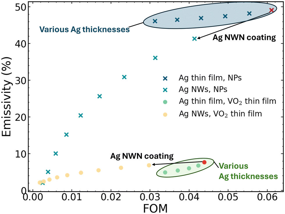 | ||
| Fig. 4 Impact on the emissivity of varying the Ag thickness vs. the impact of adding Ag NW networks with various densities. In the case of the NP stack, adding a Ag NW network yields lower ε for a given FOM, making this addition positive. In the case of the TF stack, however, it is more beneficial to use thicker Ag layers than to add a Ag NW network. The arrows point from the uncoated stack considered on which the network was added. | ||
Two distinct behaviors are observed. For NPs, thickening the Ag layer gradually decreases the emissivity with the FOM. This reduction is slower than that achieved by adding a Ag NW network, which, for a given FOM, results in lower-emissivity stacks compared to those with a thicker Ag layer but without NWs. Thus, incorporating a Ag NW network is advantageous in terms of emissivity reduction compared to simply increasing the thickness of the Ag layer, enabling the stack to achieve previously unattainable emissivities as low as 20% with FOM > 0.01. Conversely, the behavior of the TF stack offers less potential for utilizing an Ag NW network as a low emissivity add-on. Although it is possible to reduce the emissivity with dense Ag NW networks, achieving ε lower than those attainable with just a thicker Ag layer (ε < 5%) requires FOMs lower than 0.01, making the network's use less advantageous. These distinct behaviors can be explained by noting that eqn (6) predicts that the relative variation of emissivity of the stack is high for elevated substrate's emissivities, but tends towards 0 for low (<0.1) emissivities, such that the variation observed for the NP stack is greater than that for the TF stack. More details on this mechanism can be found in section S6 of the ESI.†
4 Conclusions
In the present study, we conducted a comprehensive numerical analysis to assess the influence of incorporating a silver nanowire (Ag NW) network as a low-emissivity coating on VO2-based thermochromic stacks. First, a novel figure of merit, defined as ΔTsol × T4lum, was proposed and utilized to identify an optimally performing thermochromic stack. Furthermore, our results and the exhaustive use of data from the literature also validated the numerical approach as valid when dealing with the modelling of thermochromic systems and properties. Next, we studied the integration of a thin silver layer aimed at reducing emissivity, coupled with antireflection layers SiO2 and TiO2 employed to enhance the FOM. This investigation was conducted concurrently for both a VO2 thin film and a VO2 nanoparticle-embedded PET matrix, with subsequent comparative analysis, and showed that it is theoretically possible to reach (Tlum, ΔTsol) as high as (79.4%, 11%) and (79%, 15.7%) for the TF and NP stacks, respectively. Additionally, the impact of varying the thickness of the Ag layer on the overall stack emissivity was quantified and compared to the impact of the Ag NW network coating. Our results show that while using a Ag NW network coating on a thin film-based stack did not yield a superior enhancement compared to the thicknening of the Ag thin film, it notably amplified emissivity reduction with a minimal effect on the final FOM for the nanoparticle-based system. This enhancement enabled the stack to reach a 50% relative reduction in emissivity, while maintaining luminous transmittance above 50% and solar modulation beyond 8%. The results of this research are not confined to the specific stack under examination and hold relevance for a broader range of thermochromic stack configurations.Data availability
The data that support the findings of this study are available from the corresponding author, A. Baret, upon reasonable request. The core of the simulation code can be found at https://github.com/Ethalides33/chromasolver.Conflicts of interest
There are no conflicts to declare.Acknowledgements
The authors gratefully acknowledge the financial support from the European Commission via the M-ERA.NET program (INSTEAD project). A. B. and N. D. N. acknowledge the financial support from F.R.S. – FNRS via the CDR project J.0157.24 and the PINT-MULTI project R.8012.20.References
- U. N. E. Programme and G. A. f. B. Construction, Global status report for buildings and construction, 2020 Search PubMed.
- C. G. Granqvist, Mater. Today: Proc., 2016, 3, S2–S11 Search PubMed.
- Z. Zhang, L. Zhang, Y. Zhou, Y. Cui, Z. Chen, Y. Liu, J. Li, Y. Long and Y. Gao, Chem. Rev., 2023, 123, 7025–7080 CrossRef CAS.
- Y. Cui, Y. Ke, C. Liu, Z. Chen, N. Wang, L. Zhang, Y. Zhou, S. Wang, Y. Gao and Y. Long, Joule, 2018, 2, 1707–1746 CrossRef CAS.
- Y. Zhou, S. Zhao, S. Qi, Y. Liu, N. Chen, L. Wang, Y. Niu and Q. Xu, ChemistrySelect, 2023, 8, e202302259 CrossRef CAS.
- J. Kim and T. Paik, Nanomaterials, 2021, 11, 2674 CrossRef CAS.
- K. Sun, C. Wheeler, J. A. Hillier, S. Ye, I. Zeimpekis, A. Urbani, N. Kalfagiannis, O. L. Muskens and C. H. K. de Groot, Adv. Opt. Mater., 2022, 10, 2201326 CrossRef CAS.
- L. Hu, H. Tao, G. Chen, R. Pan, M. Wan, D. Xiong and X. Zhao, J. Sol-Gel Sci. Technol., 2016, 77, 85–93 CrossRef CAS.
- W. Wu, C. Wang, C. Chen, J. Song and F. Ma, Adv. Mater. Interfaces, 2023, 10, 2202506 CrossRef CAS.
- C. Sol, M. Portnoi, T. Li, K. L. Gurunatha, J. Schläfer, S. Guldin, I. P. Parkin and I. Papakonstantinou, ACS Appl. Mater. Interfaces, 2020, 12, 8140–8145 CrossRef CAS.
- N. R. Mlyuka, G. A. Niklasson and C. G. Granqvist, Sol. Energy Mater. Sol. Cells, 2009, 93, 1685–1687 CrossRef CAS.
- N. R. Mlyuka, G. A. Niklasson and C. G. Granqvist, Phys. Status Solidi A, 2009, 206, 2155–2160 CrossRef CAS.
- J.-Q. Xi, M. F. Schubert, J. K. Kim, E. F. Schubert, M. Chen, S.-Y. Lin, W. Liu and J. A. Smart, Nat. Photonics, 2007, 1, 176–179 CrossRef CAS.
- Z. Chen, Y. Gao, L. Kang, J. Du, Z. Zhang, H. Luo, H. Miao and G. Tan, Sol. Energy Mater. Sol. Cells, 2011, 95, 2677–2684 CrossRef CAS.
- S.-H. Jeong, J.-K. Kim, B.-S. Kim, S.-H. Shim and B.-T. Lee, Vacuum, 2004, 76, 507–515 CrossRef CAS.
- B. Baloukas, S. Loquai and L. Martinu, Sol. Energy Mater. Sol. Cells, 2018, 183, 25–33 CrossRef CAS.
- W. Jin, K. Park, J. Y. Cho, S.-H. Bae, M. Siyar, H. Jang and C. Park, Ceram. Int., 2023, 49, 10437–10444 CrossRef CAS.
- T. Chang, X. Cao, L. R. Dedon, S. Long, A. Huang, Z. Shao, N. Li, H. Luo and P. Jin, Nano Energy, 2018, 44, 256–264 CrossRef CAS.
- H. Koo, D. Shin, S.-H. Bae, K.-E. Ko, S.-H. Chang and C. Park, J. Mater. Eng. Perform., 2014, 23, 402–407 CrossRef CAS.
- S. Kabir, D. Yang, A. B. Ahmad Kayani, H. Zhang, S. Nirantar, S. Sriram, S. Walia and M. Bhaskaran, ACS Appl. Nano Mater., 2022, 5, 10280–10291 CrossRef CAS.
- S.-I. Kwon, M. Hagiwara, S.-H. Kim and S. Fujihara, Int. J. Appl. Ceram. Technol., 2023, 20, 1997–2008 CrossRef CAS.
- S.-Y. Li, G. A. Niklasson and C. G. Granqvist, J. Appl. Phys., 2010, 108, 063525 CrossRef.
- Y. Cui, Y. Ke, C. Liu, Z. Chen, N. Wang, L. Zhang, Y. Zhou, S. Wang, Y. Gao and Y. Long, Joule, 2018, 2, 1707–1746 CrossRef CAS.
- N. Murillo-Quirós, V. Vega-Garita, A. Carmona-Calvo, E. A. Rojas-González, R. Starbird-Perez and E. Avendaño-Soto, Polymers, 2022, 14, 4250 CrossRef.
- J. Faucheu, E. Bourgeat-Lami and P. Vanessa, Adv. Eng. Mater., 2019, 21, 1800438 CrossRef.
- B. Li, S. Tian, L. Zhou, S. Wu, T. Ma, G. He, B. Liu and X. Zhao, Adv. Opt. Mater., 2023, 2302042 Search PubMed.
- H. Kim, D. Lahneman, C. Rohde and A. Piqué, Thin Solid Films, 2022, 759, 139455 CrossRef CAS.
- R. J. Martin-Palma, J. Nanophotonics, 2009, 3, 030305 CrossRef.
- M. Benkahoul, M. Chaker, J. Margot, E. Haddad, R. Kruzelecky, B. Wong, W. Jamroz and P. Poinas, Sol. Energy Mater. Sol. Cells, 2011, 95, 3504–3508 CrossRef CAS.
- X. Hu, W. Cai, Y. Zhang, S. Shi, Y. Ming, R. Yu, D. Chen, M. Yang, F. Wang, H. Yang, C.-W. Kan, N. Noor and B. Fei, Nano Lett., 2024, 24, 657–666 CrossRef CAS.
- R. Zhang, R. Li, P. Xu, W. Zhong, Y. Zhang, Z. Luo and B. Xiang, Chem. Eng. J., 2023, 471, 144527 CrossRef CAS.
- A. Hendaoui, N. Émond, S. Dorval, M. Chaker and E. Haddad, Sol. Energy Mater. Sol. Cells, 2013, 117, 494–498 CrossRef CAS.
- H. Kim, K. Cheung, R. C. Y. Auyeung, D. E. Wilson, K. M. Charipar, A. Piqué and N. A. Charipar, Sci. Rep., 2019, 9, 11329 CrossRef.
- X. Bowei, Z. Wenjie, Z. Junming and L. Linhua, Opt. Express, 2022, 30, 34314–34327 CrossRef PubMed.
- L. Kang, Y. Gao, Z. Chen, J. Du, Z. Zhang and H. Luo, Sol. Energy Mater. Sol. Cells, 2010, 94, 2078–2084 CrossRef CAS.
- M. C. Larciprete, A. Albertoni, A. Belardini, G. Leahu, R. Li Voti, F. Mura, C. Sibilia, I. Nefedov, I. V. Anoshkin, E. I. Kauppinen and A. G. Nasibulin, J. Appl. Phys., 2012, 112, 083503 CrossRef.
- M. Bobinger, D. Angeli, S. Colasanti, P. La Torraca, L. Larcher and P. Lugli, Phys. Status Solidi A, 2017, 214, 1600466 CrossRef.
- V. H. Nguyen, D. T. Papanastasiou, J. Resende, L. Bardet, T. Sannicolo, C. Jiménez, D. Muñoz-Rojas, N. D. Nguyen and D. Bellet, Small, 2022, 18, 2270095 CrossRef.
- D.-J. Kim, H.-I. Shin, E.-H. Ko, K.-H. Kim, T.-W. Kim and H.-K. Kim, Sci. Rep., 2016, 6, 34322 CrossRef CAS PubMed.
- L. Bardet, M. Akbari, C. Crivello, L. Rapenne, M. Weber, V. H. Nguyen, C. Jiménez, D. Muñoz-Rojas, A. Denneulin and D. Bellet, ACS Appl. Nano Mater., 2023, 6, 15234–15246 CrossRef CAS.
- A. Khan, V. H. Nguyen, D. Muñoz-Rojas, S. Aghazadehchors, C. Jiménez, N. D. Nguyen and D. Bellet, ACS Appl. Mater. Interfaces, 2018, 10, 19208–19217 CrossRef CAS.
- L. Zhao, L. Miao, C. Liu, H.-L. Wang, S. Tanemura, L. Sun, X. Gao and J. Zhou, J. Nanosci. Nanotechnol., 2015, 15, 9192–9196 CrossRef CAS.
- F. Kasten and A. T. Young, Appl. Opt., 1989, 28, 4735–4738 CrossRef CAS PubMed.
- G. Haacke, J. Appl. Phys., 1976, 47, 4086–4089 CrossRef CAS.
- S. Hanauer, C. Celle, C. Crivello, H. Szambolics, D. Muñoz-Rojas, D. Bellet and J.-P. Simonato, ACS Appl. Mater. Interfaces, 2021, 13, 21971–21978 CrossRef CAS.
- E. Pantoja, R. Bhatt, A. Liu and M. C. Gupta, Nanotechnology, 2017, 28, 505708 CrossRef PubMed.
- G. Ding, C. Clavero, G. Ding and C. Clavero, Modern Technologies for Creating the Thin-film Systems and Coatings, IntechOpen, 2017 Search PubMed.
- M. Lagrange, D. P. Langley, G. Giusti, C. Jiménez, Y. Bréchet and D. Bellet, Nanoscale, 2015, 7, 17410–17423 RSC.
- D. S. Bethune, J. Opt. Soc. Am. B, 1989, 6, 910–916 CrossRef CAS.
- M. C. Troparevsky, A. S. Sabau, A. R. Lupini and Z. Zhang, Opt. Express, 2010, 18, 24715–24721 CrossRef PubMed.
- Z. Knittl, Optics of Thin Films: An Optical Multilayer Theory, John Wiley & Sons, London, New York, 1976 Search PubMed.
- S. J. Byrnes, Multilayer Optical Calculations, 2020 Search PubMed.
- T. G. Mackay and A. Lakhtakia, The Transfer-Matrix Method in Electromagnetics and Optics, Springer International Publishing, Cham, 2020 Search PubMed.
- M. C. Troparevsky, A. S. Sabau, A. R. Lupini and Z. Zhang, Opt. Express, 2010, 18, 24715–24721 CrossRef.
- R. Ankit, WebPlotDigitizer, 2024 Search PubMed.
- J. Zheng, S. Bao and P. Jin, Nano Energy, 2015, 11, 136–145 CrossRef CAS.
- T. Chang, X. Cao, N. Li, S. Long, X. Gao, L. R. Dedon, G. Sun, H. Luo and P. Jin, ACS Appl. Mater. Interfaces, 2017, 9, 26029–26037 CrossRef CAS PubMed.
- N. R. Mlyuka, G. A. Niklasson and C. G. Granqvist, Phys. Status Solidi A, 2009, 206, 2155–2160 CrossRef CAS.
- C. Wan, Z. Zhang, D. Woolf, C. M. Hessel, J. Rensberg, J. M. Hensley, Y. Xiao, A. Shahsafi, J. Salman, S. Richter, Y. Sun, M. M. Qazilbash, R. Schmidt-Grund, C. Ronning, S. Ramanathan and M. A. Kats, Ann. Phys., 2019, 531, 1900188 CrossRef CAS.
- P. Zhao, W. Su, R. Wang, X. Xu and F. Zhang, Phys. E, 2009, 41, 387–390 CrossRef CAS.
- A. Ciesielski, L. Skowronski, M. Trzcinski and T. Szoplik, Appl. Surf. Sci., 2017, 421, 349–356 CrossRef CAS.
- I. H. Malitson, J. Opt. Soc. Am., 1965, 55, 1205–1209 CrossRef CAS.
- R. Kitamura, L. Pilon and M. Jonasz, Appl. Opt., 2007, 46, 8118–8133 CrossRef CAS PubMed.
- L. Gao, F. Lemarchand and M. Lequime, Opt. Express, 2012, 20, 15734–15751 CrossRef PubMed.
- J. Kischkat, S. Peters, B. Gruska, M. Semtsiv, M. Chashnikova, M. Klinkmüller, O. Fedosenko, S. Machulik, A. Aleksandrova, G. Monastyrskyi, Y. Flores and W. T. Masselink, Appl. Opt., 2012, 51, 6789–6798 CrossRef CAS PubMed.
- N. Herguedas and E. Carretero, Nanomaterials, 2023, 13, 2749 CrossRef CAS PubMed.
- T. Siefke, S. Kroker, K. Pfeiffer, O. Puffky, K. Dietrich, D. Franta, I. Ohlídal, A. Szeghalmi, E.-B. Kley and A. Tünnermann, Adv. Opt. Mater., 2016, 4, 1780–1786 CrossRef CAS.
- X. Zhang, J. Qiu, X. Li, J. Zhao and L. Liu, Appl. Opt., 2020, 59, 2337–2344 CrossRef CAS PubMed.
- X. Zhang, J. Qiu, J. Zhao, X. Li and L. Liu, J. Quant. Spectrosc. Radiat. Transfer, 2020, 252, 107063 CrossRef CAS.
- B. A. Rosales, J. Kim, V. M. Wheeler, L. E. Crowe, K. J. Prince, M. Mirzokarimov, T. Daligault, A. Duell, C. A. Wolden, L. T. Schelhas and L. M. Wheeler, Adv. Energy Mater., 2023, 13, 2203331 CrossRef CAS.
- W. Wu, C. Wang, C. Chen, J. Song and F. Ma, Adv. Mater. Interfaces, 2023, 10, 2202506 CrossRef CAS.
- S. Taylor, Y. Yang and L. Wang, J. Quant. Spectrosc. Radiat. Transfer, 2017, 197, 76–83 CrossRef CAS.
- A. M. Morsy, M. T. Barako, V. Jankovic, V. D. Wheeler, M. W. Knight, G. T. Papadakis, L. A. Sweatlock, P. W. C. Hon and M. L. Povinelli, Sci. Rep., 2020, 10, 13964 CrossRef CAS PubMed.
- J. Atkinson and I. A. Goldthorpe, Nanotechnology, 2020, 31, 365201 CrossRef CAS PubMed.
- P. Zhao, W. Su, R. Wang, X. Xu and F. Zhang, Phys. E, 2009, 41, 387–390 CrossRef CAS.
- T. Wenzel, J. Bosbach, F. Stietz and F. Träger, Surf. Sci., 1999, 432, 257–264 CrossRef CAS.
- J. Sang, P. Wang, Y. Meng, X. Xu, J.-L. Sun, Y. Wang, Z. Hua, T. Zheng, Z. Liu, C. Wang, B. Wu and X. Chen, Jpn. J. Appl. Phys., 2019, 58, 050917 CrossRef CAS.
- J. Domaradzki, D. Kaczmarek, M. Mazur, D. Wojcieszak, J. Halarewicz, S. Glodek and P. Domanowski, Mater. Sci., 2016, 34, 747–753 CAS.
- M. Born and E. Wolf, Principles of Optics: Electromagnetic Theory of Propagation, Interference and Diffraction of Light, Cambridge University Press, Cambridge, 7th edn, 1999 Search PubMed.
Footnote |
| † Electronic supplementary information (ESI) available. See DOI: https://doi.org/10.1039/d4lf00234b |
| This journal is © The Royal Society of Chemistry 2025 |