Recycled silicon solar cell-derived nanostructured p-black silicon device for high performance NO2 gas sensor applications†
Received
22nd August 2024
, Accepted 10th November 2024
First published on 22nd November 2024
Abstract
Nitrogen dioxide (NO2) is a toxic gas that can cause respiratory problems, and sensing its presence is crucial for environmental monitoring and industrial safety. This investigation presents a novel approach towards sensing NO2 gas by utilizing partially completed/recycled silicon solar cells employing a metal-assisted etching process to fabricate a high-performance p-black-silicon based sensor. Structural and morphological analyses using X-ray diffraction patterns, Raman spectroscopy and cross sectional FESEM characterization confirm the integrity of the p-B-silicon sensor. By combining recycling techniques with advanced fabrication methods, the resulting sensor exhibits exceptional sensitivity, a low detection limit of 1 ppm, and rapid response times (12–14 s) when exposed to NO2 gas concentrations ranging from 1 to 5 ppm. The enhanced sensitivity is attributed to the unique nanostructured comb-like morphology of the sensor material, which facilitates fast charge transport mechanisms, and a plausible sensing mechanism has been proposed and explained using a depletion model diagram and energy model diagram. This eco-friendly and cost-effective solution not only addresses electronic waste concerns but also highlights the potential of sustainable practices in scientific research. The findings emphasize on the importance of environmental consciousness and innovation, showcasing a promising future for gas sensing technology. By utilizing recycled materials and advanced fabrication techniques, this study contributes to the development of efficient, eco-friendly sensors for environmental monitoring applications, paving the way for a more sustainable and technologically advanced future in the field of gas sensors.
1. Introduction
A critical need exists for a sensor that is both reliable and swift in detecting nitrogen dioxide (NO2) gas, considering its essential contribution to environmental and health-related challenges.1,2 As a byproduct of combustion, NO2 significantly impacts smog formation, acid rain, and human health by affecting respiratory function.3,4 Controlling NO2 levels, even at room temperature, is crucial for safety, necessitating the development of high-accuracy and high-speed sensors to protect the environment and human well-being.5 Recent advancements in renewable energy technologies, especially in solar energy, have become pivotal in addressing climate change and reducing reliance on fossil fuels.6 One groundbreaking development involves repurposing half-finished solar cells to create highly efficient p-black silicon structures.7 This innovative approach not only tackles sustainability concerns by reusing materials but also leads to advanced solar cell technologies. Moreover, this breakthrough extends beyond solar energy into gas sensing applications, particularly in NO2 detection.
Silicon (Si) serves as an exceptional semiconductor for gas sensors due to its availability, low cost, and room temperature operability.8 Silicon, a cornerstone material in electronics and semiconductor industries, encompasses diverse variants such as p-B-silicon (p-type black silicone) or porous silicon, each characterized by unique properties crucial for their applications. These materials exhibit distinct bandgap widths, conduction mechanisms, and crystal structures, influencing their functionality. For instance, p-B-silicon possesses a specific bandgap width influencing its electronic properties and compatibility with processing techniques, whereas porous silicon offers a tuneable bandgap and high surface area, advantageous for sensing and optoelectronic applications. Despite their potential, challenges such as limited availability for p-B-silicon and stability concerns for porous silicon must be addressed. Advancements in understanding and harnessing these technical intricacies will propel silicon materials to broader utility in diverse technological domains. Gas sensors utilizing high surface area morphologies like micro- and nanoscale porous-Si have been developed using various fabrication methods such as electrochemical etching,9,10 plasma assisted dry etching11,12 and metal-assisted chemical etching (MACE).13–16 These sensors measure electrical and optical properties of porous-Si, relying on morphology, surface area, and reactivity for gas sensing.17–20 Ongoing research focuses on enhancing porous-Si -based sensor architectures, increasing sensitivity, selectivity, and reliability through post-treatments like rough post-etching, decorating with metal nanoparticles, employment of carbon materials, and surface chemical modifications. Hybrid structures combining porous-Si with other semiconductor materials further enhance gas-sensing capabilities. Black silicon (B-Si) shares attractive properties with porous-Si, including low reflectance, a large surface area-to-volume ratio, controllable surface morphology, superhydrophobicity, and high luminescence efficiency.21 B-Si, consisting of thin high-density silicon pyramids, demonstrates potential for gas sensing applications due to its surface characteristics and morphology.22 Recently, a wide array of B-Si based gas sensors has been created to identify particular gases, including but not limited to carbon dioxide (CO2), nitrogen dioxide (NO2), sulfur dioxide (SO2), oxygen (O2), ozone (O3), hydrogen (H2), argon (Ar), nitrogen (N2), ammonia (NH3), and various organic vapors like methanol, ethanol, isopropanol, and benzene, among others.23–25 In this study, an innovative method that utilizes partially completed/recycled silicon solar cells was used to produce p-type B-Si, offering a sustainable and cost-effective solution to electronic waste and reducing material consumption. The research further develops a high-performance p-B-silicon sensor through metal-assisted chemical etching (MACE), showcasing outstanding sensitivity, a low detection limit, and rapid response times for NO2 gas sensing at room temperature. Metal-assisted chemical etching (MACE) is a powerful technique for nanostructure fabrication, utilizing noble metal catalysts to facilitate precise etching. While metals like platinum (Pt), gold (Au), and ruthenium (Ru) have been explored, nickel (Ni) stands out for its catalytic efficiency, cost-effectiveness, and versatility. Ni exhibits high activity for surface oxidation, promoting efficient etching reactions due to favourable energetics at the Ni–semiconductor interface. Additionally, Ni's abundance and low cost make it attractive for large-scale manufacturing. The ease of Ni electroless plating with controlled deposition allows for precise control over size and morphology, enabling tailored nanostructure fabrication. Consequently, Ni-based MACE offers a promising avenue for diverse applications in nanotechnology.
In this work, we developed a resistive sensor based on black silicon (B-Si) to detect low concentrations (1–5 ppm) of NO2 at room temperature. B-Si, prepared using metal assisted chemical etching, exhibits vertically standing silicon, amplifying its surface area for efficient gas adsorption. This study aims to explore the capabilities of p-type B-Si-based sensors in detecting NO2 at low concentrations, showcasing the promise of this innovative material for gas sensing applications. Repurposing recycled solar cells in sensing applications offers a blend of environmental, economic, and technological advantages. By breathing new life into discarded materials, this approach champions sustainability, curtailing the volume of electronic waste while contributing to a greener, circular economy. The cost efficiency stemming from using recycled components further drives accessibility to sensing technologies, making them more affordable and scalable for diverse applications. Moreover, this practice stimulates innovation by encouraging creative adaptations of these materials, fostering novel sensor designs and pushing the boundaries of technological possibilities within the realm of sustainability-driven solutions.
2. Experimental
2.1 Materials
The p-type crystalline silicon (c-Si) wafers, measuring 1 cm × 1 cm, were acquired from the solar cell industry. Nickel chloride hexahydrate (NiCl2·6H2O, MERCK, 99%), sodium hypophosphite monohydrate (NaH2PO2·H2O, MERCK, 99%), ammonium chloride (NH4Cl, LOBA, 99%), and ammonia solution (NH4OH, LOBA, 99%) were utilized in the nickel electroless deposition (Ni-ED) process. Hydrofluoric acid (MERCK) and hydrogen peroxide (H2O2, LOBA, 30%) were utilized for the silicon etching process.
2.2 Nickel electroless deposition (Ni-ED)
Before commencing the Ni-ED procedure, the diced silicon wafers underwent a 5 second immersion in a 1% HF solution to eliminate the native oxide layer. Tri-ammonium citrate, sodium hypophosphite, and nickel chloride (NiCl2·6H2O) were carefully added to an optimum alkaline-based nickel electroless solution at a concentration of 20 g L−1. The purpose of this formulation was to improve the electroless deposition process's effectiveness and performance. The Ni bath, totalling 200 mL, was kept at a constant temperature of 80 ± 1 °C. The pH level of the solution was carefully regulated at 10 using NH4OH.
2.3 Characterization techniques
Recycled solar cells were the source of p-black silicon, which underwent comprehensive characterization via spectroscopic and microscopic methods. X-ray diffraction (XRD) patterns were acquired using a power X-ray diffractometer (Ultima IV, Rigaku, Japan) with Cu Kα radiation of wavelength 1.5418 Å at a scanning rate of 0.02° s−1 in the 2θ range of 20–80°. For micro Raman studies, a confocal Raman microscope (WiTec, 300 Alpha, Germany) equipped with a He–Cd laser (λ = 532 nm) as the excitation source and 600 g mm−1 gratings was utilized to analyse the p-black silicon. Additionally, the structure and morphology were assessed using a field emission scanning electron microscope (ZEISS EVO 18, US), featuring an in-built energy-dispersive X-ray spectrometer (Oxford Instruments, INCA, UK).
2.4 Etching of silicon
The wafers, which harboured nickel (Ni) nanoparticles, were subjected to an etching procedure within a meticulously controlled environment. This process involved immersing the wafers in a solution comprising hydrofluoric acid (HF), hydrogen peroxide (H2O2), and water (H2O), meticulously mixed in a ratio of 1![[thin space (1/6-em)]](https://www.rsc.org/images/entities/char_2009.gif) :5:10. The etching operation took place for a duration of 20 seconds, meticulously timed to ensure precise control over the process. All of this occurred under ambient room temperature conditions, with stringent safety measures in place, within the confines of a chemical hood to mitigate any potential hazards associated with the chemicals used.
:5:10. The etching operation took place for a duration of 20 seconds, meticulously timed to ensure precise control over the process. All of this occurred under ambient room temperature conditions, with stringent safety measures in place, within the confines of a chemical hood to mitigate any potential hazards associated with the chemicals used.
2.5 Evaluation of the performance of nitrogen dioxide (NO2) gas sensing
The sensor device was created by employing DC magnetron sputtering to deposit gold thin films, approximately 300 nm thick, directly onto the etched p-B-silicon substrate. This process involved using a laser-machined stainless-steel mask. A specially designed gas sensor test unit was utilized to examine the materials' gas sensing capabilities. The setup comprised a test chamber made of stainless steel with double walls. It featured a temperature-controlled hot stage, a holder for sensors, mass flow controllers (MFC from Alicat, USA), and a digital multimeter (Agilent 34401A, USA) that were linked to a data collection system running Labview software. Throughout the measurements, NO2 gas was diluted with dry nitrogen to produce the appropriate concentrations. The flow rate was maintained at 300 sccm utilizing mass flow controls. The regulation of the sensor's operating temperature within the sensing chamber was achieved using a temperature controller (Eurotherm, 2420, U.K.). Consistent gas pressure (710 Torr) was upheld within the sensing chamber throughout the testing, and this pressure was monitored using a Baratron 722B absolute capacitance manometer (MKS Instruments, Singapore). For interference studies, NH3, H2S, ethanol, and acetone were individually introduced to the sensor device while maintaining constant concentrations via the gas generator unit (OVG-4, U.K.). The sensor's response to each gas was measured in these controlled conditions.
3. Results and discussion
Scheme 1 illustrates the process flow adopted for p-Black silicon etching. Damaged silicon wafers, obtained in broken state from a solar cell production plant, were subjected to a meticulous process to prepare them for further use as sensors. These uneven wafers were precisely sliced into 3 cm × 3 cm dimensions using a laser cutting method. To ensure their cleanliness and purity, the sliced wafers were immersed in a heated sodium hydroxide (NaOH) solution at 80 °C for 60 s. NaOH, a strong alkaline solution, was chosen for its broad reactivity, which allows it to dissolve a wide range of contaminants, including organic residues, oils, greases, and inorganic substances. Its high reactivity, stability at elevated temperatures, affordability, and efficient rinsing properties make NaOH an ideal choice for removing diverse impurities from silicon surfaces in industrial applications. Following the NaOH cleaning step, the wafers were then immersed in a nickel electroless solution for nickel deposition, after which a silicon etching process was carried out. After the etching process, the wafers were thoroughly cleaned multiple times in DI-water.
 |
| | Scheme 1 Schematic representation of p-black silicon etching process flow. | |
3.1 Nickel electroless deposition
The electroless deposition of nickel–phosphorus (Ni–P) is an essential process in the large-scale plating and electronics industries for creating a nickel seed layer. This process involves the anodic oxidation of cathodic alloy discharge, hypophosphite, incorporation of phosphorus, and evolution of hydrogen. Among these processes, the anodic oxidation of hypophosphite is particularly significant in driving the ED process. During this ED process, nickel ions (Ni2+) from the Ni source, NiCl2·6H2O, dissociate and diffuse toward the active silicon surface, where they become adsorbed. At the catalytic surface layer, the deprotonation reaction of H2PO2− takes place. This sequence of chemical reactions forms the basis for the controlled and precise deposition of nickel–phosphorus layers, making it a vital technique in industrial applications and electronics manufacturing.
The process initiates with H2PO2− adsorbing onto the Ni2+ surface, leading to the formation of HPO2− and excess nascent hydrogen [H] (eqn (1)). However, HPO2− is highly unstable and reacts with water, resulting in the production of H2PO3−, H+, and free electrons, denoted as e− (eqn (2)). The nascent hydrogen [H] interacts with the catalytic surface, releasing free electrons (e−). These electrons then catalyse the reduction of Ni2+ ions, transforming them into stable metallic nickel, which coats the silicon surface (eqn (3)). Concurrently, the generated H+ ions accept free electrons and undergo reduction to form H2, giving rise to small bubbles observed during the electroless deposition process (eqn (4)). Additionally, phosphorus, a byproduct from the reduction of hypophosphite ions, diffuses into the nickel layer, further enriching the deposited material (eqn (5)).
| | | HPO2− + H2O → H2PO3− + H+ + e− | (2) |
| | | H2PO2− + 2H+ + e− → 2H2O + P | (5) |
Initially, nickel (Ni) ions underwent reduction on the silicon surface, giving rise to the formation of Ni nanoparticles. Due to the accumulation of Ni ions during the deposition, these nanoparticles exhibited uneven distribution and varied in size. The SEM image analysis shown in
Fig. 1(a and b) indicated that the size of these Ni particles ranged from a few nanometers to several hundred nanometers. Further
Fig. 1(c) depicts the EDX spectra which confirm the presence of nickel, phosphorus and silicon elements in the nickel deposited silicon wafer using electroless deposition.
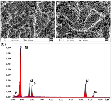 |
| | Fig. 1 (a and b) Scanning electron microscopy images and (c) EDX spectra of nickel electroless coated silicon wafer. | |
Subsequently, wafers containing these Ni nanoparticles were subjected to etching in a mixed solution of HF/H2O2/H2O (1:5:10 ratio). The highly corrosive nature of the solution led to rapid transformation of small Ni nanoparticles on the silicon wafer's surface into even smaller ones, owing to their large surface area. In contrast, the alteration of larger particles occurred at a slower pace. Ni nanoparticles of different sizes adhered to the silicon wafer surface, playing distinct roles in the reaction process. The minute Ni nanoparticles acted as catalysts in the reactions between silicon wafers and the solution, facilitating the formation of nano-pores. Conversely, the large Ni nanoparticles catalysed the creation of inverted pyramid structures. This was a consequence of these large nanoparticles gradually diminishing in size due to the solution's corrosive effects on them. Notably, despite the presence of tiny Ni nanoparticles on the silicon wafer's surface, new minute Ni particles formed upon separation from the large Ni particles due to the latter's corrosion.
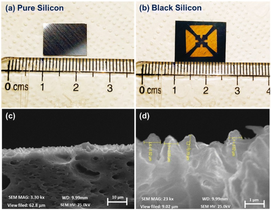
Consequently, nano-pores emerged not only on the silicon surface but also on the surfaces of the inverted pyramid structures. Fig. 2(a) shows the pristine surface cleaned silicon substrate and Fig. 2(b) shows the gold sputtered electrode contact over the surface etched black silicon device. The silicon pyramid structure has ∼0.8 μm average length and ∼0.6 μm average width as depicted in Fig. 2(c and d).
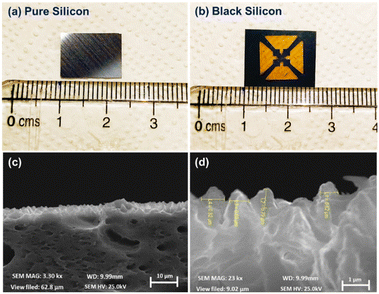 |
| | Fig. 2 (a and b) Photographs of pure and etched p-black silicon and (c and d) cross sectional FESEM images of black silicon wafer. | |
Further, to characterize the change of crystal structure in the p-B-silicon device, X-ray diffraction analysis and Raman spectroscopy were utilized. Fig. 3(a) depicts the diffraction pattern with an intense peak at 69.14° for both pure silicon and p-B-silicon. This intense peak corresponds to the (400) plane of silicon (JCPDS No. 27-1402).18,26 Owing to the formation of the pyramid like structure for p-B-silicon as observed from Fig. 2(d), the obtained diffraction pattern reveals higher intensity than pure silicon. Raman scattering measurements were performed using a confocal Raman microscope. The strong intense Raman peak arising at 522 cm−1 for the p-B-silicon device shown in Fig. 3(b) is owing to the (TO, LO) optical phonon vibration at the center Γ point of the Brillouin zone (BZ).27,28 It is revealed that the first-order scattering intensity for p-B-silicon is significantly higher than that of the pure silicon substrate. Transverse 2TA acoustical phonons exhibit a distinct second-order spectrum around 300 cm−1. A wide Raman signal located between 900 cm−1 and 1100 cm−1 is indicative of transverse optical phonons 2TO. It is rather evident that, in comparison to pure silicon, nanostructured p-B-silicon exhibits a significant amplification of multi-phonon characteristics.
 |
| | Fig. 3 (a) X-ray diffraction and (b) Raman spectra for pure silicon and the p-B-silicon device. | |
3.2 Assessment of NO2 sensing characteristics
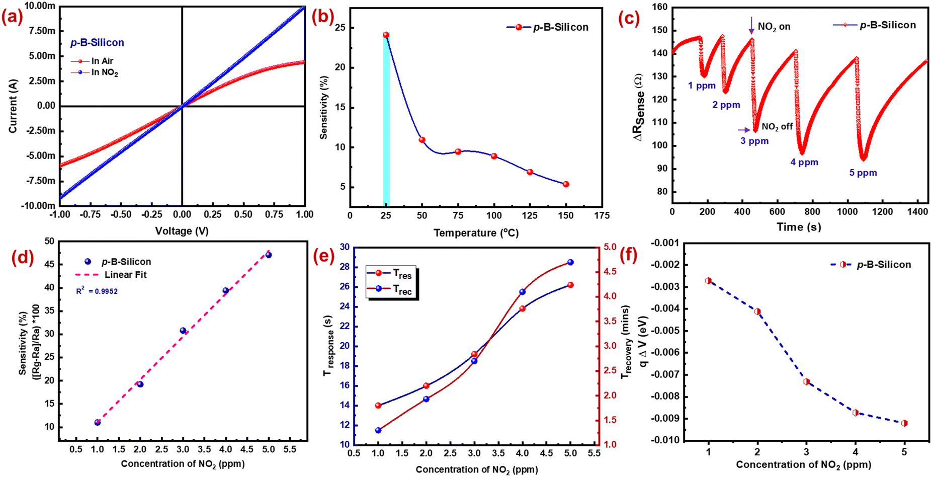
In order to speculate the NO2 sensor performance of the p-B-silicon device, the room temperature, two-probe approach was used to collect the current–voltage (I–V) plots of the as-fabricated p-B-silicon device (Fig. 4). The current–voltage (I–V) characteristics of the p-B-silicon device demonstrated linearity on gold electrodes in the range of −1 to 1 V, indicating an Ohmic behaviour (Fig. 4(a)). This ohmic trend, which demonstrates that the charge carriers can still flow freely between the sensing material and gold electrodes, suggests that the primary mechanism may be a direct charge transfer between the adsorbed NO2 molecules and the p-B-silicon device.29 As Fig. 4(a) shows, the sensor's I–V characteristics showed Ohmic behaviour under both NO2 exposure and under air flow.30 Additional research reveals that when compared to ambient atmosphere, there is an increase in current during NO2 exposure. This demonstrates the sensor device's initial confirmation of a negative trend, or a drop in resistance during NO2 purging.31 Similarly, when a reducing gas interacts with an n-type semiconductor, the same drop in resistance (negative trend) will occur.32,33
 |
| | Fig. 4 (a) Current–voltage characteristics of p-B-silicon, (b) response graph towards exposure to 2 ppm of NO2 as a function of temperature for p-B-silicon, (c) dynamic NO2 sensing characteristics of p-B-silicon, (d) NO2 response as a function of concentration, (e) NO2 response as a function of response and recovery time and (f) plot of variations in band bending energy of the p-B-silicon based sensor. | |
The NO2 gas sensing properties of p-B-silicon were evaluated by an in-house built sensor calibration test station. Since the working temperature of the material plays a decisive role in regulating the NO2 adsorption process, the optimal operating temperature of the p-B-silicon sensor was initially identified. Therefore, the sensor response, S[(Rg − Ra)/Ra] which can be estimated by purging 2 ppm of NO2 gas with respect to different temperatures from 25 °C to 150 °C, was measured and shown in Fig. 4(b) for the p-B-silicon device. The supreme sensitivity toward NO2 gas was found at room temperature itself for p-B-silicon showing 20 ± 4%, whereas the sensor response decreases with increases in temperature due to unavailability of electrons and the lack of hole mobility in the p-B-silicon device. Therefore, the optimal working temperature for the p-B-silicon system was fixed at room temperature which can be considered for further NO2 sensor calibration.
Fig. 4(c) depicts the gas sensing sensitivities of the as-fabricated p-B-silicon device to 1–5 ppm of NO2 as a function of time at room temperature (∼25 °C). The sensitivity of the p-B-silicon device was found to be maximum at ∼40.25 ± 3.3% at room temperature toward exposure to 1 to 5 ppm of NO2 gas (Fig. 4c). As can be seen, the sensitivity enhances with the increase of the concentration of NO2 gas, and reaches a maximum. The duration for a sensor to undergo 90% of the total resistance change is termed as the response or recovery time. It was observed that the response time (TRes) ranged approximately between 10 and 15 seconds, while the recovery time (TRec) was in the range of 1 to 2 minutes. At room temperature, the adsorbed oxygen molecules on etched p-B-silicon were activated to react with the NO2 gas molecules thereby enhancing its sensitivity. It is clear that, at room temperature, the sensor has a low detection limit of 1 ppm and strong detecting performance. For the purpose of sensing low concentrations of NO2 gas, the proposed sensor demonstrated improved response and recovery behavior as well as acceptable repeatability and stability. The sensor response (S) follows a linear trend as a function of NO2 concentration for the p-B-silicon based sensor device as depicted in Fig. 4(d). Moreover, the sensor response and recovery time plots are shown in Fig. 4(e). It was observed that both the sensor response and recovery time increase when the NO2 gas concentration increases. Furthermore, the surface band bending (qΔV) energies during NO2 exposure were calculated with reference to the sensor response values of the p-B-silicon device as stated in our previous report.34,35 The value of qΔV was estimated according to the NO2 response of the sensor towards different concentrations of NO2 gas. Moreover, the quantification of qΔV confirmed that the p-B-silicon device exhibits decreases in surface band bending energy with increasing NO2 concentration due to the formation of a thinning depletion region as depicted in Fig. 4(f). When the p-B-silicon device interacts with a strong oxidizing gas (NO2), it acquires hole conductivity, which causes accumulation of more holes. The study also extended to the exploration of the dynamic sensor response/recovery characteristics of the p-B-silicon sensor for higher concentrations of NO2 ranging from 5 to 25 ppm as depicted in Fig. S1(a and b).† It shows a maximum sensitivity of ∼250 ± 8% for 25 ppm of NO2. Also, Fig. S2(a and b)† depict the NO2 response of p-B-silicon sensor which has been fabricated through the MACE process on commercial and recycled silicon wafer.
The study confirms that both devices show approximately similar sensor response to 5 ppm of NO2 exposure. Since silicon-based devices are typically photosensitive, it is important to study the sensor response under light illumination. The p-B-silicon sensor was exposed to 35 W xenon light while 3 ppm of NO2 was purged. Fig. S3(a and b)† depict the response–recovery graph under light illumination and without light illumination. According to this study, p-B-silicon indicates that there is a minor variation in sensitivity and base resistance which may be due to the excitation of electrons to a higher state leading to electron–hole recombination during light illumination.36,37 Therefore, the hole mobility tends to decrease upon NO2 exposure and therefore a slightly reduced sensitivity was observed. Moreover, the selectivity to the target gas (NO2) is always one of the important challenges for gas sensing devices. Fig. 5(a) shows the measured selectivity of the p-B-silicon sensor to 2 ppm of various gas species at room temperature, including ethanol, acetone, ammonia and hydrogen sulfide. The sensor response to NO2 was much higher than those towards other tested vapours at the same concentrations at room temperature.38 The intervention of humidity on NO2 adsorption of p-B-silicon in the RH range of 20–80% is depicted in Fig. 5(b). Upon the increase in RH%, the sensitivity tends to decrease for p-B-silicon due to intervention of moisture, which persisted on the material, decreasing the hole transfer process as depicted in Fig. S4(a and b).† As RH% increases above 40%, the interference of humidity persists on p-B-silicon which can further reduce the flow of holes, and thereby decrease the rate of NO2 adsorption. Furthermore, the p-B-silicon sensor manifested an excellent response and recovery behaviour and acceptable repeatability for low concentration of (1 ppm) NO2 gas as depicted in Fig. 5(c). Interestingly, the transient response of p-B-silicon towards 10 ppm of NO2 after 3 years was acquired and is shown in Fig. 5(d). The p-B-silicon device showed appreciable constancy even after 3 years for repeated cycles of NO2 exposure. This study exemplifies the long-term stability of the p-B-silicon based sensor along with repeatability.
 |
| | Fig. 5 (a) Cross selectivity studies, (b) relative humidity interference studies, (c) repeataility studies and (d) stability studies of the p-B-silicon based sensor. | |
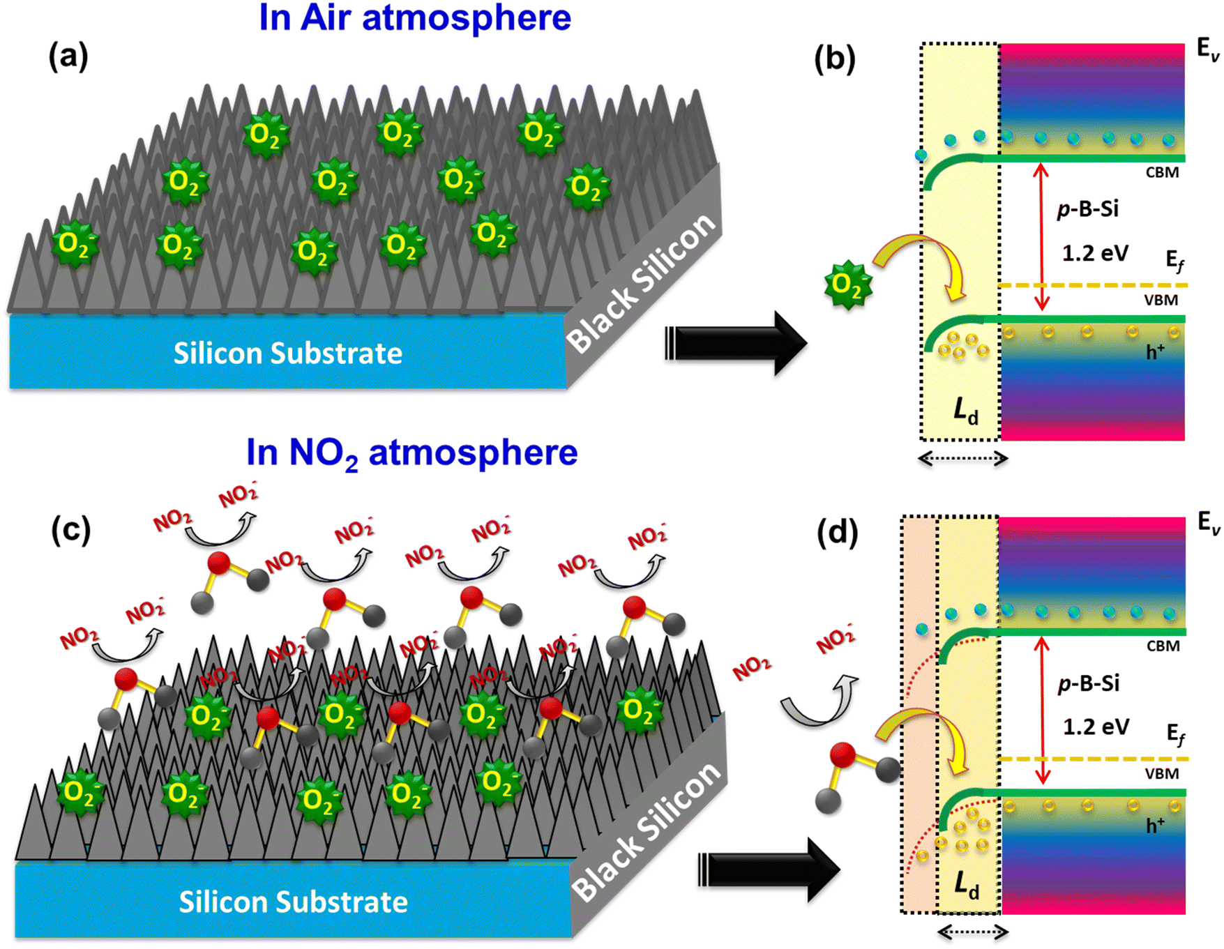
The gas sensing mechanisms of semiconductor materials are commonly explained through a space-charge layer mode, which is based on the initial dissociative chemisorption of oxygen on the sensors' surface. In the case of p-type B-silicon, in the presence of air, the surface adsorbed oxygen molecules, creating oxygen species (such as O2−, O−, and O2−) by capturing free electrons from the conductance band.39 This process results in an increase in hole concentration and a decrease in sensor resistance. When exposed to strong oxidizing gases like NO2, the adsorbed oxygen ions on the p-B-silicon surface react with the oxidizing gases, further enhancing hole accumulation and leading to an increase in the hole conductivity of the sensor device.40 A schematic representation of NO2 adsorption on the nanostructured p-B-silicon device is depicted in Scheme 2(a–d). The detection mechanism is based on the sensing behavior of p-B-silicon towards NO2 gas which can be elucidated in terms of the electron/hole transport phenomenon. The as-fabricated nanostructured p-B-silicon, exhibiting p-type conductivity with a lower bandgap, behaves like a semi-metal.39,41 When the nanostructured p-B-silicon device is exposed to oxidizing NO2 gas, the hole transport dominates rather than the electron transport thereby increasing the hole conductivity.40,42 As seen from the energy band diagram, depicted in Scheme 2(b and d), the thinning of the depletion region shows the increase in hole conduction where the holes from adsorbed NO2 molecules transfer to the valance band state of nanostructured p-B-silicon and thereby the band bends downwards further leading to the increase in the hole accumulation layer.43,44Table 1 shows the comparison of performances of NO2 sensors, which are created by the silicon etching technique.
 |
| | Scheme 2 Schematic representation of NO2 sensing mechanism of p-B-silicon sensor (a and b) in air atmosphere and (c and d) in NO2 atmosphere. | |
Table 1 Performance comparison of NO2 sensing properties of Si-based NO2 gas sensors
| Material, |
Etching method |
Post-treatment |
Concentration [ppm] |
Gas response |
Response/recovery time [s] |
Ref. |
| p-Type B-Si |
Metal assisted chemical etching |
Ni (electroless deposition) |
1 |
11 |
14/∼75 |
This work |
| BSi, p-type |
Reactive ion etching |
Pristine |
4 |
52 |
35/25 |
29
|
| Nano-PSi, p-type |
Metal assisted chemical etching |
Pristine |
10 |
9.56 |
80/410 |
18
|
| Nano-PSi, n-type |
Metal assisted chemical etching |
Pristine |
10 |
1.16 |
64/68 |
45
|
| Micro-PSi, p-type |
Electrochemical etching |
Hybrid CuO |
2 |
87 |
51/547 |
34
|
| Micro-PSi, p-type |
Electrochemical etching |
NPs Au, hybrid WO3 |
1 |
5.16 |
28/721 |
46
|
| Nano-PSi, n-type |
Metal assisted chemical etching |
NPs ZnO |
50 |
10 |
>300 |
47
|
Conclusions
In summary, this study introduces a groundbreaking method for NO2 gas sensing by repurposing partially completed silicon solar cells and utilizing a metal-assisted etching technique to create a high-performance p-B-silicon sensor. By combining recycling methods with advanced fabrication techniques, we have developed a sensor that exhibits remarkable sensitivity, a low detection limit, and rapid response times. The structure and morphology of the p-B-silicon sensor were analysed using Raman spectroscopy and cross sectional FESEM characterization, confirming its integrity. The sensor based on p-B-silicon demonstrated superior sensitivity to NO2 gas within the range of 1–5 ppm, with an impressively low detection limit of 1 ppm and rapid response time (tres(90)) of 12–14 seconds. This heightened sensitivity to NO2 gas can be attributed to its nanostructured comb-like morphology, which facilitates swift charge transport mechanisms. This environmentally friendly and cost-effective approach not only addresses concerns related to electronic waste but also exemplifies the potential of sustainable practices in scientific research. The outcomes of this study contribute to the advancement of gas sensing technology and underscore the significance of environmental awareness and innovation in shaping a sustainable future.
Data availability
The data that support the findings of this study are available from the corresponding author upon reasonable request.
Author contributions
M. A. and R. V. have equally contributed in writing the main manuscript, validation, methodology, investigation, formal analysis, data curation, and conceptualization. B. P.: supervision, project administration, validation, resource, review and editing the manuscript.
Conflicts of interest
The authors declare that they have no conflict of interest.
Acknowledgements
We gratefully acknowledge DST-WTI for financial support (DST/TMD-EWO/WTI/2K19/EWFH/2019/273). We acknowledge the facilities and support provided by the management of PSG Sons and Charities, Coimbatore, India. The author R. V. gratefully acknowledges the Ministry of Education (India) through the FAST grant of F. No. 5-6/2013-TS.VII and the Department of Science and Technology (DST; India) through the FIST grant of SR/FST/ETI-416/2016 at Center of Excellence in Advanced Materials and Green Technologies, Amrita School of Engineering Coimbatore, Amrita Vishwa Vidyapeetham, India for the support.
References
- W. de Vries, Impacts of nitrogen emissions on ecosystems and human health: A mini review, Curr. Opin. Environ. Sci. Health, 2021, 21, 100249 CrossRef.
- K. Sur, V. K. Verma and B. Pateriya, Variation of tropospheric NO2 over Indo-Gangetic plain during COVID-19 outbreak in India, Spat. Inf. Res., 2021, 29, 841–855 CrossRef.
- I. Manisalidis, E. Stavropoulou, A. Stavropoulos and E. Bezirtzoglou, Environmental and Health Impacts of Air Pollution: A Review, Front. Public Health, 2020, 8, 1–13 CrossRef.
- Y. Guo, L. Zhu, X. Wang, X. Qiu, W. Qian and L. Wang, Assessing environmental impact of NOX and SO2 emissions in textiles production with chemical footprint, Sci. Total Environ., 2022, 831, 154961 CrossRef CAS.
- M. Akbari-Saatlu, M. Procek, C. Mattsson, G. Thungström, H. E. Nilsson, W. Xiong, B. Xu, Y. Li and H. H. Radamson, Silicon nanowires for gas sensing: A review, Nanomaterials, 2020, 10, 1–57 CrossRef PubMed.
- M. Aleem, K. K. Karuppanan, A. V. Raghu, N. Satheesan, B. Krishnan and B. Pullithadathil, Optimal Design of Narrow Line-Width Front Contact Grid Pattern for Silicon Solar Cells and Low-Cost Fabrication of Electroless Nickel Plated Imprint Lithography Hard Stamp, Adv. Eng. Mater., 2019, 21, 1–11 CrossRef.
- M. Aleem, R. Vishnuraj, B. Krishnan and B. Pullithadathil, Realization of Micropatterned, Narrow Line-Width Ni-Cu-Sn Front Contact Grid Pattern Using Maskless Direct-Write Lithography for Industrial Silicon Solar Cells, ACS Appl. Energy Mater., 2021, 4, 10682–10696 CrossRef CAS.
- M. Aleem, R. Vishnuraj, B. Krishnan, A. Ashok and B. Pullithadathil, Narrow Line Width Ni–Cu–Sn Front Contact Metallization Patterns for Low-Cost High-Efficiency Crystalline Silicon Solar Cells using Nano-Imprint Lithography, Energy Technol., 2023, 11, 1–13 Search PubMed.
- X. Yang, F. Xi, X. Chen, S. Li, X. Wan, W. Ma, P. Dong, J. Duan and Y. Chang, Porous Silicon Fabrication and Surface Cracking Behavior Research Based on Anodic Electrochemical Etching, Fuel Cells, 2021, 21, 52–57 CrossRef CAS.
- D. Ge, J. Wei, J. Ding, J. Zhang, C. Ma, M. Wang, L. Zhang and S. Zhu, Silver Nano-Dendrite-Plated Porous Silicon Substrates Formed by Single-Step Electrochemical Synthesis for Surface-Enhanced Raman Scattering, ACS Appl. Nano Mater., 2020, 3, 3011–3018 CrossRef CAS.
- X. Liu, B. Radfar, K. Chen, O. E. Setala, T. P. Pasanen, M. Yli-Koski, H. Savin and V. Vahanissi, Perspectives on Black Silicon in Semiconductor Manufacturing: Experimental Comparison of Plasma Etching, MACE, and Fs-Laser Etching, IEEE Trans. Semicond. Manuf., 2022, 35, 504–510 Search PubMed.
- I. Morozov, A. Gudovskikh, A. Uvarov, A. Baranov, V. Sivakov and D. Kudryashov, The Study of Latex Sphere Lithography for High Aspect Ratio Dry Silicon Etching, Phys. Status Solidi A, 2020, 217, 1–6 CrossRef.
- H. Fan, Y. Si, Y. Zhang, F. Zhu, X. Wang and Y. Fu, Grapevine-like high entropy oxide composites boost high-performance lithium sulfur batteries as bifunctional interlayers, Green Energy Environ., 2024, 9, 565–572 CrossRef CAS.
- S. D. Wang, S. Y. Chen, S. P. Hsu, C. Y. Liao and W. Y. Hsu, Ag and Cu metal-assisted chemical etching for diamond-wire-sawn single-crystalline silicon solar cell, Appl. Surf. Sci., 2022, 578, 152050 CrossRef CAS.
- H. Han, Z. Huang and W. Lee, Metal-assisted chemical etching of silicon and nanotechnology applications, Nano Today, 2014, 9, 271–304 CrossRef CAS.
- A. Backes and U. Schmid, Impact of doping level on the metal assisted chemical etching of p-type silicon, Sens. Actuators, B, 2014, 193, 883–887 CrossRef CAS.
- N. S. A. Eom, H. B. Cho, H. R. Lim, T. Y. Hwang, Y. Song and Y. H. Choa, Ultrasensitive detection of low-ppm H2S gases based on palladium-doped porous silicon sensors, RSC Adv., 2018, 8, 29995–30001 RSC.
- M. S. Choi, H. G. Na, A. Mirzaei, J. H. Bang, W. Oum, S. Han, S. W. Choi, M. Kim, C. Jin, S. S. Kim and H. W. Kim, Room-temperature NO2 sensor based on electrochemically etched porous silicon, J. Alloys Compd., 2019, 811, 151975 CrossRef CAS.
- S. Zhu, X. Liu, J. Zhuang and L. Zhao, A fast room temperature NH3 sensor based on an Al/p-Si/Al structure with schottky electrodes, Sensors, 2017, 17, 1–9 Search PubMed.
- N. S. A. Eom, H. B. Cho, Y. Song, W. Lee, T. Sekino and Y. H. Choa, Room-temperature H2 gas sensing characterization of graphene-doped porous silicon via a facile solution dropping method, Sensors, 2017, 17, 1–7 Search PubMed.
- K. Hassan, A. S. M. I. Uddin and G. S. Chung, Hydrogen sensing properties of Pt/Pd bimetal decorated on highly hydrophobic Si nanowires, Int. J. Hydrogen Energy, 2016, 41, 10991–11001 CrossRef CAS.
- R. Ahmad, S. M. Majhi, X. Zhang, T. M. Swager and K. N. Salama, Recent progress and perspectives of gas sensors based on vertically oriented ZnO nanomaterials, Adv. Colloid Interface Sci., 2019, 270, 1–27 CrossRef CAS PubMed.
- J. B. Maurya, Y. K. Prajapati, S. Raikwar and J. P. Saini, A silicon-black phosphorous based surface plasmon resonance sensor for the detection of NO2 gas, Optik, 2018, 160, 428–433 CrossRef CAS.
- P. Raju and Q. Li, Review—Semiconductor Materials and Devices for Gas Sensors, J. Electrochem. Soc., 2022, 169, 057518 CrossRef CAS.
- S. Yousef, M. Tatariants, M. Tichonovas and V. Makarevicius, Sustainable technology for mass production of Ag nanoparticles and Al microparticles from damaged solar cell wafers, Waste Manage., 2019, 98, 126–134 CrossRef CAS.
- M. Naffeti, P. A. Postigo, R. Chtourou and M. A. Zaïbi, Elucidating the effect of etching time key-parameter toward optically and electrically-active silicon nanowires, Nanomaterials, 2020, 10(3), 404 CrossRef CAS.
- M. Ivanda, O. Gamulin and W. Kiefer, Mechanism of Raman scattering in amorphous silicon, J. Mol. Struct., 1999, 480–481, 651–655 CrossRef CAS.
- W. Wei, One- and two-phonon Raman scattering from hydrogenated nanocrystalline silicon films, Vacuum, 2007, 81, 857–865 CrossRef CAS.
- G. Ayvazyan, K. Ayvazyan, L. Hakhoyan and A. Semchenko, NO2 Gas Sensor Based on Pristine Black Silicon Formed by Reactive Ion Etching, Phys. Status Solidi RRL, 2023, 17, 1–8 Search PubMed.
- W. Wang, S. Ma, X. Liu, Y. Zhao, H. Li, Y. Li, X. Ning, L. Zhao and J. Zhuang, NO2 gas sensor with excellent performance based on thermally modified nitrogen-hyperdoped silicon, Sens. Actuators, B, 2022, 354, 131193 CrossRef CAS.
- S. Y. Jeong, S. Jeong, S. W. Lee, S. T. Kim, D. Kim, H. J. Jeong, J. T. Han, K. J. Baeg, S. Yang, M. S. Jeong and G. W. Lee, Enhanced response and sensitivity of self-corrugated graphene sensors with anisotropic charge distribution, Sci. Rep., 2015, 5, 1–9 Search PubMed.
- X. Shao, D. Zhang, M. Tang, H. Zhang, Z. Wang, P. Jia and J. Zhai, Amorphous Ag catalytic layer-SnO2 sensitive layer-graphite carbon nitride electron supply layer synergy-enhanced hydrogen gas sensor, Chem. Eng. J., 2024, 495, 153676 CrossRef CAS.
- M. Tang, Z. Wang, D. Wang, R. Mao, H. Zhang, W. Xu, Z. Yang and D. Zhang, Construction of LaF3 QD-modified SnS2 nanorod composites for ultrasensitive detection of H2S, J. Mater. Chem. A, 2023, 11, 9942–9954 RSC.
- X. Liu, M. Hu, Y. Wang, J. Liu and Y. Qin, High sensitivity NO2 sensor based on CuO/p-porous silicon heterojunction at room temperature, J. Alloys Compd., 2016, 685, 364–369 CrossRef CAS.
- R. Vishnuraj, K. K. Karuppanan, M. Aleem and B. Pullithadathil, Boosting the performance of NO2gas sensors based on n-n type mesoporous ZnO@In2O3heterojunction nanowires: in situconducting probe atomic force microscopic elucidation of room temperature local electron transport, Nanoscale Adv., 2020, 2, 4785–4797 RSC.
- F. Unal, M. S. Kurt and S. Durdu, Investigation of the effect of light on the electrical parameters of Si/TiO2 heterojunctions produced by anodic oxidation on p-type Si wafer, J. Mater. Sci.: Mater. Electron., 2022, 33, 15834–15847 CrossRef CAS.
- R. Peter, A. Omerzu, I. Kavre Piltaver, R. Speranza, K. Salamon, M. Podlogar, K. Velican, M. Percic and M. Petravic, Large enhancement of visible light photocatalytic efficiency of ZnO films doped in-situ by copper during atomic layer deposition growth, Ceram. Int., 2023, 49, 35229–35238 CrossRef CAS.
- W. Meng, S. Wu, X. Wang and D. Zhang, High-sensitivity resistive humidity sensor based on graphitic carbon nitride nanosheets and its application, Sens. Actuators, B, 2020, 315, 128058 CrossRef CAS.
- A. Iefanova, N. Adhikari, A. Dubey, D. Khatiwada and Q. Qiao, Lead free CH3NH3SnI3 perovskite thin-film with p-type semiconducting nature and metal-like conductivity, AIP Adv., 2016, 6(8), 085312 CrossRef.
- B. G. Krishna, D. S. Ghosh and S. Tiwari, Hole and electron transport materials: A review on recent progress in organic charge transport materials for efficient, stable, and scalable perovskite solar cells, Chem. Inorg. Mater., 2023, 1, 100026 Search PubMed.
- V. Ramakrishnan, K. K. Karuppanan, M. Aleem and B. Pullithadathil, Boosting Performance of NO2 Gas Sensor based on n-n Type Mesoporous ZnO@In2O3 Heterojunction Nanowires: In-situ Conducting Probe Atomic Force Microscopic Elucidation of Room Temperature, Localized Electron Transfer, Nanoscale Adv., 2020, 2(10), 4785–4797 RSC.
- S. Li, Y. L. Cao, W. H. Li and Z. S. Bo, A brief review of hole transporting materials commonly used in perovskite solar cells, Rare Met., 2021, 40, 2712–2729 CrossRef CAS.
- Y. Yang, B. Xu and J. Hou, Reducing Depletion Region Width at Electrode Interface via a Hole-transport Layer for Over 18% Efficiency in Organic Solar Cells, Small, 2023, 2306668, 1–9 Search PubMed.
- R. Vishnuraj, R. Unnathpadi, M. Rangarajan and B. Pullithadathil, n–n type In2O3@-WO3 heterojunction nanowires: enhanced NO2 gas sensing characteristics for environmental monitoring, Microchim. Acta, 2024, 191, 645 CrossRef CAS PubMed.
- Y. J. Kwon, A. Mirzaei, H. G. Na, S. Y. Kang, M. S. Choi, J. H. Bang, W. Oum, S. S. Kim and H. W. Kim, Porous Si nanowires for highly selective room-Temperature NO2 gas sensing, Nanotechnology, 2018, 29(29), 294001 CrossRef PubMed.
- L. Yuan, M. Hu, Y. Wei and W. Ma, Enhanced NO2 sensing characteristics of Au modified porous silicon/thorn-sphere-like tungsten oxide composites, Appl. Surf. Sci., 2016, 389, 824–834 CrossRef CAS.
- J. Liao, Z. Li, G. Wang, C. Chen, S. Lv and M. Li, ZnO nanorod/porous silicon nanowire hybrid structures as highly-sensitive NO2 gas sensors at room temperature, Phys. Chem. Chem. Phys., 2016, 18, 4835–4841 RSC.
|
| This journal is © The Royal Society of Chemistry 2025 |
Click here to see how this site uses Cookies. View our privacy policy here. 
 Open Access Article
 This Open Access Article is licensed under a Creative Commons Attribution-Non Commercial 3.0 Unported Licence
 *a
*a